CN100401503C - Semiconductor device and manufacturing method of the same - Google Patents
Semiconductor device and manufacturing method of the same Download PDFInfo
- Publication number
- CN100401503C CN100401503C CNB2005100738045A CN200510073804A CN100401503C CN 100401503 C CN100401503 C CN 100401503C CN B2005100738045 A CNB2005100738045 A CN B2005100738045A CN 200510073804 A CN200510073804 A CN 200510073804A CN 100401503 C CN100401503 C CN 100401503C
- Authority
- CN
- China
- Prior art keywords
- semiconductor device
- semiconductor chip
- semiconductor
- wiring layer
- hole
- Prior art date
- Legal status (The legal status is an assumption and is not a legal conclusion. Google has not performed a legal analysis and makes no representation as to the accuracy of the status listed.)
- Expired - Fee Related
Links
- 239000004065 semiconductor Substances 0.000 title claims abstract description 177
- 238000004519 manufacturing process Methods 0.000 title claims abstract description 25
- 239000000758 substrate Substances 0.000 claims abstract description 77
- 238000000034 method Methods 0.000 claims abstract description 34
- 230000015572 biosynthetic process Effects 0.000 claims description 19
- 239000000945 filler Substances 0.000 claims description 11
- 230000004069 differentiation Effects 0.000 claims 1
- 230000000149 penetrating effect Effects 0.000 abstract 1
- 239000010410 layer Substances 0.000 description 30
- 238000005755 formation reaction Methods 0.000 description 15
- 238000005530 etching Methods 0.000 description 9
- 239000010949 copper Substances 0.000 description 6
- ATJFFYVFTNAWJD-UHFFFAOYSA-N Tin Chemical compound [Sn] ATJFFYVFTNAWJD-UHFFFAOYSA-N 0.000 description 4
- 238000005538 encapsulation Methods 0.000 description 4
- RYGMFSIKBFXOCR-UHFFFAOYSA-N Copper Chemical compound [Cu] RYGMFSIKBFXOCR-UHFFFAOYSA-N 0.000 description 3
- 229910052802 copper Inorganic materials 0.000 description 3
- 229920005989 resin Polymers 0.000 description 3
- 239000011347 resin Substances 0.000 description 3
- 229910052581 Si3N4 Inorganic materials 0.000 description 2
- VYPSYNLAJGMNEJ-UHFFFAOYSA-N Silicium dioxide Chemical compound O=[Si]=O VYPSYNLAJGMNEJ-UHFFFAOYSA-N 0.000 description 2
- 239000003822 epoxy resin Substances 0.000 description 2
- 239000002184 metal Substances 0.000 description 2
- 229910052751 metal Inorganic materials 0.000 description 2
- 238000007747 plating Methods 0.000 description 2
- 229920000647 polyepoxide Polymers 0.000 description 2
- 230000001105 regulatory effect Effects 0.000 description 2
- HQVNEWCFYHHQES-UHFFFAOYSA-N silicon nitride Chemical compound N12[Si]34N5[Si]62N3[Si]51N64 HQVNEWCFYHHQES-UHFFFAOYSA-N 0.000 description 2
- 229910052814 silicon oxide Inorganic materials 0.000 description 2
- 238000004544 sputter deposition Methods 0.000 description 2
- 229910000838 Al alloy Inorganic materials 0.000 description 1
- BQCADISMDOOEFD-UHFFFAOYSA-N Silver Chemical compound [Ag] BQCADISMDOOEFD-UHFFFAOYSA-N 0.000 description 1
- 239000004411 aluminium Substances 0.000 description 1
- 229910052782 aluminium Inorganic materials 0.000 description 1
- XAGFODPZIPBFFR-UHFFFAOYSA-N aluminium Chemical compound [Al] XAGFODPZIPBFFR-UHFFFAOYSA-N 0.000 description 1
- 230000006378 damage Effects 0.000 description 1
- 238000005516 engineering process Methods 0.000 description 1
- 238000010438 heat treatment Methods 0.000 description 1
- 238000009434 installation Methods 0.000 description 1
- 239000000463 material Substances 0.000 description 1
- 239000000203 mixture Substances 0.000 description 1
- 239000011241 protective layer Substances 0.000 description 1
- 229910052709 silver Inorganic materials 0.000 description 1
- 239000004332 silver Substances 0.000 description 1
Images


Classifications
-
- H—ELECTRICITY
- H01—ELECTRIC ELEMENTS
- H01L—SEMICONDUCTOR DEVICES NOT COVERED BY CLASS H10
- H01L23/00—Details of semiconductor or other solid state devices
- H01L23/02—Containers; Seals
- H01L23/04—Containers; Seals characterised by the shape of the container or parts, e.g. caps, walls
- H01L23/053—Containers; Seals characterised by the shape of the container or parts, e.g. caps, walls the container being a hollow construction and having an insulating or insulated base as a mounting for the semiconductor body
- H01L23/055—Containers; Seals characterised by the shape of the container or parts, e.g. caps, walls the container being a hollow construction and having an insulating or insulated base as a mounting for the semiconductor body the leads having a passage through the base
-
- H—ELECTRICITY
- H05—ELECTRIC TECHNIQUES NOT OTHERWISE PROVIDED FOR
- H05K—PRINTED CIRCUITS; CASINGS OR CONSTRUCTIONAL DETAILS OF ELECTRIC APPARATUS; MANUFACTURE OF ASSEMBLAGES OF ELECTRICAL COMPONENTS
- H05K3/00—Apparatus or processes for manufacturing printed circuits
- H05K3/30—Assembling printed circuits with electric components, e.g. with resistor
- H05K3/32—Assembling printed circuits with electric components, e.g. with resistor electrically connecting electric components or wires to printed circuits
- H05K3/34—Assembling printed circuits with electric components, e.g. with resistor electrically connecting electric components or wires to printed circuits by soldering
- H05K3/341—Surface mounted components
- H05K3/3431—Leadless components
- H05K3/3442—Leadless components having edge contacts, e.g. leadless chip capacitors, chip carriers
-
- H—ELECTRICITY
- H01—ELECTRIC ELEMENTS
- H01L—SEMICONDUCTOR DEVICES NOT COVERED BY CLASS H10
- H01L21/00—Processes or apparatus adapted for the manufacture or treatment of semiconductor or solid state devices or of parts thereof
- H01L21/02—Manufacture or treatment of semiconductor devices or of parts thereof
- H01L21/04—Manufacture or treatment of semiconductor devices or of parts thereof the devices having at least one potential-jump barrier or surface barrier, e.g. PN junction, depletion layer or carrier concentration layer
- H01L21/50—Assembly of semiconductor devices using processes or apparatus not provided for in a single one of the subgroups H01L21/06 - H01L21/326, e.g. sealing of a cap to a base of a container
- H01L21/56—Encapsulations, e.g. encapsulation layers, coatings
-
- H—ELECTRICITY
- H01—ELECTRIC ELEMENTS
- H01L—SEMICONDUCTOR DEVICES NOT COVERED BY CLASS H10
- H01L21/00—Processes or apparatus adapted for the manufacture or treatment of semiconductor or solid state devices or of parts thereof
- H01L21/67—Apparatus specially adapted for handling semiconductor or electric solid state devices during manufacture or treatment thereof; Apparatus specially adapted for handling wafers during manufacture or treatment of semiconductor or electric solid state devices or components ; Apparatus not specifically provided for elsewhere
- H01L21/683—Apparatus specially adapted for handling semiconductor or electric solid state devices during manufacture or treatment thereof; Apparatus specially adapted for handling wafers during manufacture or treatment of semiconductor or electric solid state devices or components ; Apparatus not specifically provided for elsewhere for supporting or gripping
- H01L21/6835—Apparatus specially adapted for handling semiconductor or electric solid state devices during manufacture or treatment thereof; Apparatus specially adapted for handling wafers during manufacture or treatment of semiconductor or electric solid state devices or components ; Apparatus not specifically provided for elsewhere for supporting or gripping using temporarily an auxiliary support
-
- H—ELECTRICITY
- H01—ELECTRIC ELEMENTS
- H01L—SEMICONDUCTOR DEVICES NOT COVERED BY CLASS H10
- H01L21/00—Processes or apparatus adapted for the manufacture or treatment of semiconductor or solid state devices or of parts thereof
- H01L21/70—Manufacture or treatment of devices consisting of a plurality of solid state components formed in or on a common substrate or of parts thereof; Manufacture of integrated circuit devices or of parts thereof
- H01L21/71—Manufacture of specific parts of devices defined in group H01L21/70
- H01L21/768—Applying interconnections to be used for carrying current between separate components within a device comprising conductors and dielectrics
- H01L21/76898—Applying interconnections to be used for carrying current between separate components within a device comprising conductors and dielectrics formed through a semiconductor substrate
-
- H—ELECTRICITY
- H01—ELECTRIC ELEMENTS
- H01L—SEMICONDUCTOR DEVICES NOT COVERED BY CLASS H10
- H01L21/00—Processes or apparatus adapted for the manufacture or treatment of semiconductor or solid state devices or of parts thereof
- H01L21/70—Manufacture or treatment of devices consisting of a plurality of solid state components formed in or on a common substrate or of parts thereof; Manufacture of integrated circuit devices or of parts thereof
- H01L21/77—Manufacture or treatment of devices consisting of a plurality of solid state components or integrated circuits formed in, or on, a common substrate
- H01L21/78—Manufacture or treatment of devices consisting of a plurality of solid state components or integrated circuits formed in, or on, a common substrate with subsequent division of the substrate into plural individual devices
-
- H—ELECTRICITY
- H01—ELECTRIC ELEMENTS
- H01L—SEMICONDUCTOR DEVICES NOT COVERED BY CLASS H10
- H01L23/00—Details of semiconductor or other solid state devices
- H01L23/12—Mountings, e.g. non-detachable insulating substrates
-
- H—ELECTRICITY
- H01—ELECTRIC ELEMENTS
- H01L—SEMICONDUCTOR DEVICES NOT COVERED BY CLASS H10
- H01L23/00—Details of semiconductor or other solid state devices
- H01L23/48—Arrangements for conducting electric current to or from the solid state body in operation, e.g. leads, terminal arrangements ; Selection of materials therefor
- H01L23/481—Internal lead connections, e.g. via connections, feedthrough structures
-
- H—ELECTRICITY
- H01—ELECTRIC ELEMENTS
- H01L—SEMICONDUCTOR DEVICES NOT COVERED BY CLASS H10
- H01L24/00—Arrangements for connecting or disconnecting semiconductor or solid-state bodies; Methods or apparatus related thereto
- H01L24/01—Means for bonding being attached to, or being formed on, the surface to be connected, e.g. chip-to-package, die-attach, "first-level" interconnects; Manufacturing methods related thereto
- H01L24/02—Bonding areas ; Manufacturing methods related thereto
- H01L24/03—Manufacturing methods
-
- H—ELECTRICITY
- H01—ELECTRIC ELEMENTS
- H01L—SEMICONDUCTOR DEVICES NOT COVERED BY CLASS H10
- H01L24/00—Arrangements for connecting or disconnecting semiconductor or solid-state bodies; Methods or apparatus related thereto
- H01L24/01—Means for bonding being attached to, or being formed on, the surface to be connected, e.g. chip-to-package, die-attach, "first-level" interconnects; Manufacturing methods related thereto
- H01L24/02—Bonding areas ; Manufacturing methods related thereto
- H01L24/04—Structure, shape, material or disposition of the bonding areas prior to the connecting process
- H01L24/05—Structure, shape, material or disposition of the bonding areas prior to the connecting process of an individual bonding area
-
- H—ELECTRICITY
- H01—ELECTRIC ELEMENTS
- H01L—SEMICONDUCTOR DEVICES NOT COVERED BY CLASS H10
- H01L2221/00—Processes or apparatus adapted for the manufacture or treatment of semiconductor or solid state devices or of parts thereof covered by H01L21/00
- H01L2221/67—Apparatus for handling semiconductor or electric solid state devices during manufacture or treatment thereof; Apparatus for handling wafers during manufacture or treatment of semiconductor or electric solid state devices or components; Apparatus not specifically provided for elsewhere
- H01L2221/683—Apparatus for handling semiconductor or electric solid state devices during manufacture or treatment thereof; Apparatus for handling wafers during manufacture or treatment of semiconductor or electric solid state devices or components; Apparatus not specifically provided for elsewhere for supporting or gripping
- H01L2221/68304—Apparatus for handling semiconductor or electric solid state devices during manufacture or treatment thereof; Apparatus for handling wafers during manufacture or treatment of semiconductor or electric solid state devices or components; Apparatus not specifically provided for elsewhere for supporting or gripping using temporarily an auxiliary support
- H01L2221/6834—Apparatus for handling semiconductor or electric solid state devices during manufacture or treatment thereof; Apparatus for handling wafers during manufacture or treatment of semiconductor or electric solid state devices or components; Apparatus not specifically provided for elsewhere for supporting or gripping using temporarily an auxiliary support used to protect an active side of a device or wafer
-
- H—ELECTRICITY
- H01—ELECTRIC ELEMENTS
- H01L—SEMICONDUCTOR DEVICES NOT COVERED BY CLASS H10
- H01L2224/00—Indexing scheme for arrangements for connecting or disconnecting semiconductor or solid-state bodies and methods related thereto as covered by H01L24/00
- H01L2224/01—Means for bonding being attached to, or being formed on, the surface to be connected, e.g. chip-to-package, die-attach, "first-level" interconnects; Manufacturing methods related thereto
- H01L2224/02—Bonding areas; Manufacturing methods related thereto
- H01L2224/023—Redistribution layers [RDL] for bonding areas
- H01L2224/0237—Disposition of the redistribution layers
- H01L2224/02371—Disposition of the redistribution layers connecting the bonding area on a surface of the semiconductor or solid-state body with another surface of the semiconductor or solid-state body
-
- H—ELECTRICITY
- H01—ELECTRIC ELEMENTS
- H01L—SEMICONDUCTOR DEVICES NOT COVERED BY CLASS H10
- H01L2224/00—Indexing scheme for arrangements for connecting or disconnecting semiconductor or solid-state bodies and methods related thereto as covered by H01L24/00
- H01L2224/01—Means for bonding being attached to, or being formed on, the surface to be connected, e.g. chip-to-package, die-attach, "first-level" interconnects; Manufacturing methods related thereto
- H01L2224/02—Bonding areas; Manufacturing methods related thereto
- H01L2224/023—Redistribution layers [RDL] for bonding areas
- H01L2224/0237—Disposition of the redistribution layers
- H01L2224/02377—Fan-in arrangement
-
- H—ELECTRICITY
- H01—ELECTRIC ELEMENTS
- H01L—SEMICONDUCTOR DEVICES NOT COVERED BY CLASS H10
- H01L2224/00—Indexing scheme for arrangements for connecting or disconnecting semiconductor or solid-state bodies and methods related thereto as covered by H01L24/00
- H01L2224/01—Means for bonding being attached to, or being formed on, the surface to be connected, e.g. chip-to-package, die-attach, "first-level" interconnects; Manufacturing methods related thereto
- H01L2224/02—Bonding areas; Manufacturing methods related thereto
- H01L2224/04—Structure, shape, material or disposition of the bonding areas prior to the connecting process
- H01L2224/0401—Bonding areas specifically adapted for bump connectors, e.g. under bump metallisation [UBM]
-
- H—ELECTRICITY
- H01—ELECTRIC ELEMENTS
- H01L—SEMICONDUCTOR DEVICES NOT COVERED BY CLASS H10
- H01L2224/00—Indexing scheme for arrangements for connecting or disconnecting semiconductor or solid-state bodies and methods related thereto as covered by H01L24/00
- H01L2224/01—Means for bonding being attached to, or being formed on, the surface to be connected, e.g. chip-to-package, die-attach, "first-level" interconnects; Manufacturing methods related thereto
- H01L2224/02—Bonding areas; Manufacturing methods related thereto
- H01L2224/04—Structure, shape, material or disposition of the bonding areas prior to the connecting process
- H01L2224/05—Structure, shape, material or disposition of the bonding areas prior to the connecting process of an individual bonding area
- H01L2224/05001—Internal layers
- H01L2224/05099—Material
- H01L2224/051—Material with a principal constituent of the material being a metal or a metalloid, e.g. boron [B], silicon [Si], germanium [Ge], arsenic [As], antimony [Sb], tellurium [Te] and polonium [Po], and alloys thereof
- H01L2224/05117—Material with a principal constituent of the material being a metal or a metalloid, e.g. boron [B], silicon [Si], germanium [Ge], arsenic [As], antimony [Sb], tellurium [Te] and polonium [Po], and alloys thereof the principal constituent melting at a temperature of greater than or equal to 400°C and less than 950°C
- H01L2224/05124—Aluminium [Al] as principal constituent
-
- H—ELECTRICITY
- H01—ELECTRIC ELEMENTS
- H01L—SEMICONDUCTOR DEVICES NOT COVERED BY CLASS H10
- H01L2224/00—Indexing scheme for arrangements for connecting or disconnecting semiconductor or solid-state bodies and methods related thereto as covered by H01L24/00
- H01L2224/01—Means for bonding being attached to, or being formed on, the surface to be connected, e.g. chip-to-package, die-attach, "first-level" interconnects; Manufacturing methods related thereto
- H01L2224/02—Bonding areas; Manufacturing methods related thereto
- H01L2224/04—Structure, shape, material or disposition of the bonding areas prior to the connecting process
- H01L2224/05—Structure, shape, material or disposition of the bonding areas prior to the connecting process of an individual bonding area
- H01L2224/05001—Internal layers
- H01L2224/05099—Material
- H01L2224/051—Material with a principal constituent of the material being a metal or a metalloid, e.g. boron [B], silicon [Si], germanium [Ge], arsenic [As], antimony [Sb], tellurium [Te] and polonium [Po], and alloys thereof
- H01L2224/05138—Material with a principal constituent of the material being a metal or a metalloid, e.g. boron [B], silicon [Si], germanium [Ge], arsenic [As], antimony [Sb], tellurium [Te] and polonium [Po], and alloys thereof the principal constituent melting at a temperature of greater than or equal to 950°C and less than 1550°C
- H01L2224/05147—Copper [Cu] as principal constituent
-
- H—ELECTRICITY
- H01—ELECTRIC ELEMENTS
- H01L—SEMICONDUCTOR DEVICES NOT COVERED BY CLASS H10
- H01L2224/00—Indexing scheme for arrangements for connecting or disconnecting semiconductor or solid-state bodies and methods related thereto as covered by H01L24/00
- H01L2224/01—Means for bonding being attached to, or being formed on, the surface to be connected, e.g. chip-to-package, die-attach, "first-level" interconnects; Manufacturing methods related thereto
- H01L2224/02—Bonding areas; Manufacturing methods related thereto
- H01L2224/04—Structure, shape, material or disposition of the bonding areas prior to the connecting process
- H01L2224/05—Structure, shape, material or disposition of the bonding areas prior to the connecting process of an individual bonding area
- H01L2224/0554—External layer
- H01L2224/05541—Structure
- H01L2224/05548—Bonding area integrally formed with a redistribution layer on the semiconductor or solid-state body
-
- H—ELECTRICITY
- H01—ELECTRIC ELEMENTS
- H01L—SEMICONDUCTOR DEVICES NOT COVERED BY CLASS H10
- H01L2224/00—Indexing scheme for arrangements for connecting or disconnecting semiconductor or solid-state bodies and methods related thereto as covered by H01L24/00
- H01L2224/01—Means for bonding being attached to, or being formed on, the surface to be connected, e.g. chip-to-package, die-attach, "first-level" interconnects; Manufacturing methods related thereto
- H01L2224/02—Bonding areas; Manufacturing methods related thereto
- H01L2224/04—Structure, shape, material or disposition of the bonding areas prior to the connecting process
- H01L2224/05—Structure, shape, material or disposition of the bonding areas prior to the connecting process of an individual bonding area
- H01L2224/0554—External layer
- H01L2224/0556—Disposition
- H01L2224/05568—Disposition the whole external layer protruding from the surface
-
- H—ELECTRICITY
- H01—ELECTRIC ELEMENTS
- H01L—SEMICONDUCTOR DEVICES NOT COVERED BY CLASS H10
- H01L2224/00—Indexing scheme for arrangements for connecting or disconnecting semiconductor or solid-state bodies and methods related thereto as covered by H01L24/00
- H01L2224/01—Means for bonding being attached to, or being formed on, the surface to be connected, e.g. chip-to-package, die-attach, "first-level" interconnects; Manufacturing methods related thereto
- H01L2224/02—Bonding areas; Manufacturing methods related thereto
- H01L2224/04—Structure, shape, material or disposition of the bonding areas prior to the connecting process
- H01L2224/05—Structure, shape, material or disposition of the bonding areas prior to the connecting process of an individual bonding area
- H01L2224/0554—External layer
- H01L2224/05599—Material
- H01L2224/056—Material with a principal constituent of the material being a metal or a metalloid, e.g. boron [B], silicon [Si], germanium [Ge], arsenic [As], antimony [Sb], tellurium [Te] and polonium [Po], and alloys thereof
- H01L2224/05617—Material with a principal constituent of the material being a metal or a metalloid, e.g. boron [B], silicon [Si], germanium [Ge], arsenic [As], antimony [Sb], tellurium [Te] and polonium [Po], and alloys thereof the principal constituent melting at a temperature of greater than or equal to 400°C and less than 950°C
- H01L2224/05624—Aluminium [Al] as principal constituent
-
- H—ELECTRICITY
- H01—ELECTRIC ELEMENTS
- H01L—SEMICONDUCTOR DEVICES NOT COVERED BY CLASS H10
- H01L2224/00—Indexing scheme for arrangements for connecting or disconnecting semiconductor or solid-state bodies and methods related thereto as covered by H01L24/00
- H01L2224/01—Means for bonding being attached to, or being formed on, the surface to be connected, e.g. chip-to-package, die-attach, "first-level" interconnects; Manufacturing methods related thereto
- H01L2224/02—Bonding areas; Manufacturing methods related thereto
- H01L2224/04—Structure, shape, material or disposition of the bonding areas prior to the connecting process
- H01L2224/05—Structure, shape, material or disposition of the bonding areas prior to the connecting process of an individual bonding area
- H01L2224/0554—External layer
- H01L2224/05599—Material
- H01L2224/056—Material with a principal constituent of the material being a metal or a metalloid, e.g. boron [B], silicon [Si], germanium [Ge], arsenic [As], antimony [Sb], tellurium [Te] and polonium [Po], and alloys thereof
- H01L2224/05638—Material with a principal constituent of the material being a metal or a metalloid, e.g. boron [B], silicon [Si], germanium [Ge], arsenic [As], antimony [Sb], tellurium [Te] and polonium [Po], and alloys thereof the principal constituent melting at a temperature of greater than or equal to 950°C and less than 1550°C
- H01L2224/05647—Copper [Cu] as principal constituent
-
- H—ELECTRICITY
- H01—ELECTRIC ELEMENTS
- H01L—SEMICONDUCTOR DEVICES NOT COVERED BY CLASS H10
- H01L2224/00—Indexing scheme for arrangements for connecting or disconnecting semiconductor or solid-state bodies and methods related thereto as covered by H01L24/00
- H01L2224/01—Means for bonding being attached to, or being formed on, the surface to be connected, e.g. chip-to-package, die-attach, "first-level" interconnects; Manufacturing methods related thereto
- H01L2224/10—Bump connectors; Manufacturing methods related thereto
- H01L2224/12—Structure, shape, material or disposition of the bump connectors prior to the connecting process
- H01L2224/13—Structure, shape, material or disposition of the bump connectors prior to the connecting process of an individual bump connector
- H01L2224/13001—Core members of the bump connector
- H01L2224/1302—Disposition
- H01L2224/13023—Disposition the whole bump connector protruding from the surface
-
- H—ELECTRICITY
- H01—ELECTRIC ELEMENTS
- H01L—SEMICONDUCTOR DEVICES NOT COVERED BY CLASS H10
- H01L2224/00—Indexing scheme for arrangements for connecting or disconnecting semiconductor or solid-state bodies and methods related thereto as covered by H01L24/00
- H01L2224/01—Means for bonding being attached to, or being formed on, the surface to be connected, e.g. chip-to-package, die-attach, "first-level" interconnects; Manufacturing methods related thereto
- H01L2224/10—Bump connectors; Manufacturing methods related thereto
- H01L2224/12—Structure, shape, material or disposition of the bump connectors prior to the connecting process
- H01L2224/13—Structure, shape, material or disposition of the bump connectors prior to the connecting process of an individual bump connector
- H01L2224/13001—Core members of the bump connector
- H01L2224/1302—Disposition
- H01L2224/13024—Disposition the bump connector being disposed on a redistribution layer on the semiconductor or solid-state body
-
- H—ELECTRICITY
- H01—ELECTRIC ELEMENTS
- H01L—SEMICONDUCTOR DEVICES NOT COVERED BY CLASS H10
- H01L2224/00—Indexing scheme for arrangements for connecting or disconnecting semiconductor or solid-state bodies and methods related thereto as covered by H01L24/00
- H01L2224/01—Means for bonding being attached to, or being formed on, the surface to be connected, e.g. chip-to-package, die-attach, "first-level" interconnects; Manufacturing methods related thereto
- H01L2224/10—Bump connectors; Manufacturing methods related thereto
- H01L2224/12—Structure, shape, material or disposition of the bump connectors prior to the connecting process
- H01L2224/13—Structure, shape, material or disposition of the bump connectors prior to the connecting process of an individual bump connector
- H01L2224/13001—Core members of the bump connector
- H01L2224/13099—Material
-
- H—ELECTRICITY
- H01—ELECTRIC ELEMENTS
- H01L—SEMICONDUCTOR DEVICES NOT COVERED BY CLASS H10
- H01L2224/00—Indexing scheme for arrangements for connecting or disconnecting semiconductor or solid-state bodies and methods related thereto as covered by H01L24/00
- H01L2224/01—Means for bonding being attached to, or being formed on, the surface to be connected, e.g. chip-to-package, die-attach, "first-level" interconnects; Manufacturing methods related thereto
- H01L2224/10—Bump connectors; Manufacturing methods related thereto
- H01L2224/15—Structure, shape, material or disposition of the bump connectors after the connecting process
- H01L2224/16—Structure, shape, material or disposition of the bump connectors after the connecting process of an individual bump connector
- H01L2224/161—Disposition
- H01L2224/16104—Disposition relative to the bonding area, e.g. bond pad
- H01L2224/16105—Disposition relative to the bonding area, e.g. bond pad the bump connector connecting bonding areas being not aligned with respect to each other
-
- H—ELECTRICITY
- H01—ELECTRIC ELEMENTS
- H01L—SEMICONDUCTOR DEVICES NOT COVERED BY CLASS H10
- H01L2224/00—Indexing scheme for arrangements for connecting or disconnecting semiconductor or solid-state bodies and methods related thereto as covered by H01L24/00
- H01L2224/01—Means for bonding being attached to, or being formed on, the surface to be connected, e.g. chip-to-package, die-attach, "first-level" interconnects; Manufacturing methods related thereto
- H01L2224/26—Layer connectors, e.g. plate connectors, solder or adhesive layers; Manufacturing methods related thereto
- H01L2224/28—Structure, shape, material or disposition of the layer connectors prior to the connecting process
- H01L2224/29—Structure, shape, material or disposition of the layer connectors prior to the connecting process of an individual layer connector
- H01L2224/29001—Core members of the layer connector
- H01L2224/29099—Material
- H01L2224/2919—Material with a principal constituent of the material being a polymer, e.g. polyester, phenolic based polymer, epoxy
-
- H—ELECTRICITY
- H01—ELECTRIC ELEMENTS
- H01L—SEMICONDUCTOR DEVICES NOT COVERED BY CLASS H10
- H01L2224/00—Indexing scheme for arrangements for connecting or disconnecting semiconductor or solid-state bodies and methods related thereto as covered by H01L24/00
- H01L2224/80—Methods for connecting semiconductor or other solid state bodies using means for bonding being attached to, or being formed on, the surface to be connected
- H01L2224/81—Methods for connecting semiconductor or other solid state bodies using means for bonding being attached to, or being formed on, the surface to be connected using a bump connector
- H01L2224/812—Applying energy for connecting
- H01L2224/8121—Applying energy for connecting using a reflow oven
-
- H—ELECTRICITY
- H01—ELECTRIC ELEMENTS
- H01L—SEMICONDUCTOR DEVICES NOT COVERED BY CLASS H10
- H01L2224/00—Indexing scheme for arrangements for connecting or disconnecting semiconductor or solid-state bodies and methods related thereto as covered by H01L24/00
- H01L2224/80—Methods for connecting semiconductor or other solid state bodies using means for bonding being attached to, or being formed on, the surface to be connected
- H01L2224/81—Methods for connecting semiconductor or other solid state bodies using means for bonding being attached to, or being formed on, the surface to be connected using a bump connector
- H01L2224/818—Bonding techniques
- H01L2224/81801—Soldering or alloying
- H01L2224/81815—Reflow soldering
-
- H—ELECTRICITY
- H01—ELECTRIC ELEMENTS
- H01L—SEMICONDUCTOR DEVICES NOT COVERED BY CLASS H10
- H01L2224/00—Indexing scheme for arrangements for connecting or disconnecting semiconductor or solid-state bodies and methods related thereto as covered by H01L24/00
- H01L2224/80—Methods for connecting semiconductor or other solid state bodies using means for bonding being attached to, or being formed on, the surface to be connected
- H01L2224/83—Methods for connecting semiconductor or other solid state bodies using means for bonding being attached to, or being formed on, the surface to be connected using a layer connector
- H01L2224/838—Bonding techniques
- H01L2224/8385—Bonding techniques using a polymer adhesive, e.g. an adhesive based on silicone, epoxy, polyimide, polyester
- H01L2224/83851—Bonding techniques using a polymer adhesive, e.g. an adhesive based on silicone, epoxy, polyimide, polyester being an anisotropic conductive adhesive
-
- H—ELECTRICITY
- H01—ELECTRIC ELEMENTS
- H01L—SEMICONDUCTOR DEVICES NOT COVERED BY CLASS H10
- H01L2224/00—Indexing scheme for arrangements for connecting or disconnecting semiconductor or solid-state bodies and methods related thereto as covered by H01L24/00
- H01L2224/93—Batch processes
- H01L2224/94—Batch processes at wafer-level, i.e. with connecting carried out on a wafer comprising a plurality of undiced individual devices
-
- H—ELECTRICITY
- H01—ELECTRIC ELEMENTS
- H01L—SEMICONDUCTOR DEVICES NOT COVERED BY CLASS H10
- H01L23/00—Details of semiconductor or other solid state devices
- H01L23/28—Encapsulations, e.g. encapsulating layers, coatings, e.g. for protection
- H01L23/31—Encapsulations, e.g. encapsulating layers, coatings, e.g. for protection characterised by the arrangement or shape
- H01L23/3107—Encapsulations, e.g. encapsulating layers, coatings, e.g. for protection characterised by the arrangement or shape the device being completely enclosed
- H01L23/3114—Encapsulations, e.g. encapsulating layers, coatings, e.g. for protection characterised by the arrangement or shape the device being completely enclosed the device being a chip scale package, e.g. CSP
-
- H—ELECTRICITY
- H01—ELECTRIC ELEMENTS
- H01L—SEMICONDUCTOR DEVICES NOT COVERED BY CLASS H10
- H01L24/00—Arrangements for connecting or disconnecting semiconductor or solid-state bodies; Methods or apparatus related thereto
- H01L24/01—Means for bonding being attached to, or being formed on, the surface to be connected, e.g. chip-to-package, die-attach, "first-level" interconnects; Manufacturing methods related thereto
- H01L24/10—Bump connectors ; Manufacturing methods related thereto
- H01L24/11—Manufacturing methods
-
- H—ELECTRICITY
- H01—ELECTRIC ELEMENTS
- H01L—SEMICONDUCTOR DEVICES NOT COVERED BY CLASS H10
- H01L24/00—Arrangements for connecting or disconnecting semiconductor or solid-state bodies; Methods or apparatus related thereto
- H01L24/01—Means for bonding being attached to, or being formed on, the surface to be connected, e.g. chip-to-package, die-attach, "first-level" interconnects; Manufacturing methods related thereto
- H01L24/10—Bump connectors ; Manufacturing methods related thereto
- H01L24/12—Structure, shape, material or disposition of the bump connectors prior to the connecting process
- H01L24/13—Structure, shape, material or disposition of the bump connectors prior to the connecting process of an individual bump connector
-
- H—ELECTRICITY
- H01—ELECTRIC ELEMENTS
- H01L—SEMICONDUCTOR DEVICES NOT COVERED BY CLASS H10
- H01L24/00—Arrangements for connecting or disconnecting semiconductor or solid-state bodies; Methods or apparatus related thereto
- H01L24/01—Means for bonding being attached to, or being formed on, the surface to be connected, e.g. chip-to-package, die-attach, "first-level" interconnects; Manufacturing methods related thereto
- H01L24/10—Bump connectors ; Manufacturing methods related thereto
- H01L24/15—Structure, shape, material or disposition of the bump connectors after the connecting process
- H01L24/16—Structure, shape, material or disposition of the bump connectors after the connecting process of an individual bump connector
-
- H—ELECTRICITY
- H01—ELECTRIC ELEMENTS
- H01L—SEMICONDUCTOR DEVICES NOT COVERED BY CLASS H10
- H01L24/00—Arrangements for connecting or disconnecting semiconductor or solid-state bodies; Methods or apparatus related thereto
- H01L24/80—Methods for connecting semiconductor or other solid state bodies using means for bonding being attached to, or being formed on, the surface to be connected
- H01L24/81—Methods for connecting semiconductor or other solid state bodies using means for bonding being attached to, or being formed on, the surface to be connected using a bump connector
-
- H—ELECTRICITY
- H01—ELECTRIC ELEMENTS
- H01L—SEMICONDUCTOR DEVICES NOT COVERED BY CLASS H10
- H01L24/00—Arrangements for connecting or disconnecting semiconductor or solid-state bodies; Methods or apparatus related thereto
- H01L24/80—Methods for connecting semiconductor or other solid state bodies using means for bonding being attached to, or being formed on, the surface to be connected
- H01L24/83—Methods for connecting semiconductor or other solid state bodies using means for bonding being attached to, or being formed on, the surface to be connected using a layer connector
-
- H—ELECTRICITY
- H01—ELECTRIC ELEMENTS
- H01L—SEMICONDUCTOR DEVICES NOT COVERED BY CLASS H10
- H01L29/00—Semiconductor devices adapted for rectifying, amplifying, oscillating or switching, or capacitors or resistors with at least one potential-jump barrier or surface barrier, e.g. PN junction depletion layer or carrier concentration layer; Details of semiconductor bodies or of electrodes thereof ; Multistep manufacturing processes therefor
- H01L29/02—Semiconductor bodies ; Multistep manufacturing processes therefor
- H01L29/06—Semiconductor bodies ; Multistep manufacturing processes therefor characterised by their shape; characterised by the shapes, relative sizes, or dispositions of the semiconductor regions ; characterised by the concentration or distribution of impurities within semiconductor regions
- H01L29/0657—Semiconductor bodies ; Multistep manufacturing processes therefor characterised by their shape; characterised by the shapes, relative sizes, or dispositions of the semiconductor regions ; characterised by the concentration or distribution of impurities within semiconductor regions characterised by the shape of the body
-
- H—ELECTRICITY
- H01—ELECTRIC ELEMENTS
- H01L—SEMICONDUCTOR DEVICES NOT COVERED BY CLASS H10
- H01L2924/00—Indexing scheme for arrangements or methods for connecting or disconnecting semiconductor or solid-state bodies as covered by H01L24/00
- H01L2924/0001—Technical content checked by a classifier
- H01L2924/0002—Not covered by any one of groups H01L24/00, H01L24/00 and H01L2224/00
-
- H—ELECTRICITY
- H01—ELECTRIC ELEMENTS
- H01L—SEMICONDUCTOR DEVICES NOT COVERED BY CLASS H10
- H01L2924/00—Indexing scheme for arrangements or methods for connecting or disconnecting semiconductor or solid-state bodies as covered by H01L24/00
- H01L2924/01—Chemical elements
- H01L2924/01013—Aluminum [Al]
-
- H—ELECTRICITY
- H01—ELECTRIC ELEMENTS
- H01L—SEMICONDUCTOR DEVICES NOT COVERED BY CLASS H10
- H01L2924/00—Indexing scheme for arrangements or methods for connecting or disconnecting semiconductor or solid-state bodies as covered by H01L24/00
- H01L2924/01—Chemical elements
- H01L2924/01029—Copper [Cu]
-
- H—ELECTRICITY
- H01—ELECTRIC ELEMENTS
- H01L—SEMICONDUCTOR DEVICES NOT COVERED BY CLASS H10
- H01L2924/00—Indexing scheme for arrangements or methods for connecting or disconnecting semiconductor or solid-state bodies as covered by H01L24/00
- H01L2924/01—Chemical elements
- H01L2924/01033—Arsenic [As]
-
- H—ELECTRICITY
- H01—ELECTRIC ELEMENTS
- H01L—SEMICONDUCTOR DEVICES NOT COVERED BY CLASS H10
- H01L2924/00—Indexing scheme for arrangements or methods for connecting or disconnecting semiconductor or solid-state bodies as covered by H01L24/00
- H01L2924/01—Chemical elements
- H01L2924/01047—Silver [Ag]
-
- H—ELECTRICITY
- H01—ELECTRIC ELEMENTS
- H01L—SEMICONDUCTOR DEVICES NOT COVERED BY CLASS H10
- H01L2924/00—Indexing scheme for arrangements or methods for connecting or disconnecting semiconductor or solid-state bodies as covered by H01L24/00
- H01L2924/01—Chemical elements
- H01L2924/01078—Platinum [Pt]
-
- H—ELECTRICITY
- H01—ELECTRIC ELEMENTS
- H01L—SEMICONDUCTOR DEVICES NOT COVERED BY CLASS H10
- H01L2924/00—Indexing scheme for arrangements or methods for connecting or disconnecting semiconductor or solid-state bodies as covered by H01L24/00
- H01L2924/013—Alloys
- H01L2924/014—Solder alloys
-
- H—ELECTRICITY
- H01—ELECTRIC ELEMENTS
- H01L—SEMICONDUCTOR DEVICES NOT COVERED BY CLASS H10
- H01L2924/00—Indexing scheme for arrangements or methods for connecting or disconnecting semiconductor or solid-state bodies as covered by H01L24/00
- H01L2924/10—Details of semiconductor or other solid state devices to be connected
- H01L2924/1015—Shape
- H01L2924/10155—Shape being other than a cuboid
- H01L2924/10156—Shape being other than a cuboid at the periphery
-
- H—ELECTRICITY
- H05—ELECTRIC TECHNIQUES NOT OTHERWISE PROVIDED FOR
- H05K—PRINTED CIRCUITS; CASINGS OR CONSTRUCTIONAL DETAILS OF ELECTRIC APPARATUS; MANUFACTURE OF ASSEMBLAGES OF ELECTRICAL COMPONENTS
- H05K2201/00—Indexing scheme relating to printed circuits covered by H05K1/00
- H05K2201/03—Conductive materials
- H05K2201/0332—Structure of the conductor
- H05K2201/0364—Conductor shape
- H05K2201/0367—Metallic bump or raised conductor not used as solder bump
-
- H—ELECTRICITY
- H05—ELECTRIC TECHNIQUES NOT OTHERWISE PROVIDED FOR
- H05K—PRINTED CIRCUITS; CASINGS OR CONSTRUCTIONAL DETAILS OF ELECTRIC APPARATUS; MANUFACTURE OF ASSEMBLAGES OF ELECTRICAL COMPONENTS
- H05K2201/00—Indexing scheme relating to printed circuits covered by H05K1/00
- H05K2201/09—Shape and layout
- H05K2201/09145—Edge details
- H05K2201/09154—Bevelled, chamferred or tapered edge
-
- H—ELECTRICITY
- H05—ELECTRIC TECHNIQUES NOT OTHERWISE PROVIDED FOR
- H05K—PRINTED CIRCUITS; CASINGS OR CONSTRUCTIONAL DETAILS OF ELECTRIC APPARATUS; MANUFACTURE OF ASSEMBLAGES OF ELECTRICAL COMPONENTS
- H05K2201/00—Indexing scheme relating to printed circuits covered by H05K1/00
- H05K2201/20—Details of printed circuits not provided for in H05K2201/01 - H05K2201/10
- H05K2201/2036—Permanent spacer or stand-off in a printed circuit or printed circuit assembly
-
- Y—GENERAL TAGGING OF NEW TECHNOLOGICAL DEVELOPMENTS; GENERAL TAGGING OF CROSS-SECTIONAL TECHNOLOGIES SPANNING OVER SEVERAL SECTIONS OF THE IPC; TECHNICAL SUBJECTS COVERED BY FORMER USPC CROSS-REFERENCE ART COLLECTIONS [XRACs] AND DIGESTS
- Y02—TECHNOLOGIES OR APPLICATIONS FOR MITIGATION OR ADAPTATION AGAINST CLIMATE CHANGE
- Y02P—CLIMATE CHANGE MITIGATION TECHNOLOGIES IN THE PRODUCTION OR PROCESSING OF GOODS
- Y02P70/00—Climate change mitigation technologies in the production process for final industrial or consumer products
- Y02P70/50—Manufacturing or production processes characterised by the final manufactured product
Abstract
The purpose of the invention is provide a semiconductor device capable of improving a mounting strength and a mounting accuracy without making processes complex, and a method of manufacturing the semiconductor device. Grooves 14 are formed on a rear face of a semiconductor substrate 10 along a dicing line DL. Furthermore, there are formed via holes 16 penetrating the semiconductor substrate 10 from the rear face thereof to pad electrodes 11. Embedded electrodes 18 are then formed in the via holes 16 and there is formed a wiring layer 19 which is connected with the embedded electrodes 18 and extends to a region near the dicing line DL. Conductive terminals 21 are formed at end portions of the wiring layer 19. Then, by dicing along the dicing line DL, a semiconductor device 1 having inclined surfaces Is at end portions of a rear face thereof is completed. When the semiconductor device 1 is connected with a circuit board 30 by a reflow process, conductive pastes having increased fluidity cover the conductive terminals 21 and the inclined surfaces 1s. In this case, conductive pastes 40a, 40b containing side fillets are formed on the circuit board 30 around an outer edge of the semiconductor device 1.
Description
Technical field
The present invention relates to semiconductor device and manufacture method thereof, particularly relate to encapsulation type semiconductor device and manufacture method thereof.
Background technology
In recent years, as the encapsulation type semiconductor device, CSP (chip size packages Chip Size Package) is subjected to people's attention.CSP is the compact package that has with the overall dimension of the overall dimension approximate same size of semiconductor chip.
At present, CSP's is a kind of, and BGA (welded ball array Ball GridArray) N-type semiconductor N device is arranged as can be known.In this BGA N-type semiconductor N device, a plurality of spherical conducting terminals that are made of metal partss such as scolding tin are arranged on clathrate ground on an interarea of encapsulation, and it is electrically connected with semiconductor chip on other interarea that is equipped on encapsulation.Below, with reference to the BGA N-type semiconductor N device of description of drawings conventional example.
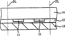
Fig. 9 is the profile of the semiconductor device of explanation conventional example.As shown in Figure 9, be formed with pad electrode 61 on the surface of the semiconductor chip 60A of semiconductor device 2.In addition, semiconductor chip 60A surperficial sealed 63 (or supporting mass) covers.On semiconductor chip 60A, be formed with the through hole that penetrates into pad electrode 61 from this back side.In this through hole, be formed with the embedded electrode 68 that is connected with pad electrode 61.On the embedded electrode 68 that the through hole at the semiconductor chip 60A back side exposes, be formed with spherical conducting terminal 71.
This semiconductor device 2 makes circuitry substrate 80 and semiconductor chip backside subtend on being installed on the circuitry substrate 80 that is formed with not shown conductive pattern the time, is arranged on this circuitry substrate 80.At this, on the interarea of the circuitry substrate 80 that is formed with not shown conductive pattern, print process is formed with the conductive paste 90 that is made of for example scolding tin for example utilizing with conducting terminal 71 position contacting.In addition, on the interarea of circuitry substrate 80, be formed with the so-called underfilling 91 that is used to prevent between the back side of semiconductor chip 60A and circuitry substrate 80, produce the space in the zone that does not form conductive paste 90.
Conductive paste 90 increases mobile by reflow treatment, partly cover conducting terminal 71.Thus, the not shown conductive pattern of conducting terminal 71 and circuitry substrate 80 is electrically connected, and simultaneously, is fixed on the circuitry substrate 80.
In addition, Guan Lian technical literature can be enumerated for example following patent documentation.
Patent documentation 1: the spy opens the 2003-309221 communique
Patent documentation 2: special table 2002-512436 communique
Patent documentation 3: the spy opens the 2003-229518 communique
But,, have the problem that produces bad connection being situated between when connecting the semiconductor device 2 of above-mentioned conventional example and circuitry substrate 80 by conductive paste 90.This be because, the amount that is formed at the conductive paste 90 on the circuitry substrate 80 is restricted on a small quantity, so sometimes when reflow treatment, conductive paste 90 can not flow on the not shown conductive pattern of conducting terminal 71 and circuitry substrate 80 exactly.In addition, when solving above-mentioned bad connection and increase the amount of conductive paste 90, when having produced reflow treatment more than conductive paste make the such problem of adjacent conductive terminal 71 short circuits.In addition, be difficult to confirm whether correctly connecting.
In addition, by conductive paste 90 semiconductor device 2 correctly is connected with circuitry substrate 80, but because the amount of conductive paste is few, so the mechanical strength during connection is also not enough even be situated between.Therefore, between semiconductor chip 60A and circuitry substrate 80, form the so-called underfilling that constitutes by epoxy resin etc., suppress the short circuit of 71 of conducting terminals, simultaneously, strengthen above-mentioned mechanical strength.The formation of this underfilling is undertaken by the user of semiconductor device usually, so the operation when existing the user to install increases such problem.
The result is, the complex procedures the during user installation of semiconductor device, and the precision when installing reduces.Therefore, the invention provides a kind of semiconductor device and manufacture method thereof, it can not make complex procedures, and can improve intensity and precision when installing.
Summary of the invention
Semiconductor device of the present invention is developed in view of above-mentioned problem, and it provides a kind of semiconductor device, and mounting has following feature on circuitry substrate.
That is, semiconductor device of the present invention comprises: semiconductor chip; Pad electrode, it is formed on the surface of semiconductor chip; The inclined plane, its side from the sloped-end of semiconductor chip backside to this semiconductor chip; Through hole, it penetrates into the surface of pad electrode from semiconductor chip backside; Dielectric film, it is formed on the semiconductor chip backside of the sidewall that contains through hole; Embedded electrode, it is formed in the through hole via dielectric film, and is electrically connected with pad electrode; Wiring layer, it is formed on via dielectric film and contains through hole on interior semiconductor chip backside, is connected with embedded electrode, and extends on the inclined plane of semiconductor chip.At this, semiconductor device makes circuitry substrate and mounting relative with semiconductor chip backside on circuitry substrate.In addition, semiconductor device of the present invention has the conducting terminal that is formed on the wiring layer on the basis of said structure.
Semiconductor device of the present invention is formed with the conductivity filler rod that covers the wiring layer (comprising conducting terminal when forming conducting terminal) that reaches on the embedded electrode on the described inclined plane in the end at the semiconductor chip back side on the basis of said structure.In addition, semiconductor device of the present invention is formed with supporting mass on the surface of semiconductor chip on the basis of said structure.
The invention provides a kind of manufacture method of semiconductor device, it is characterized in that, comprising: prepare to distinguish, and form the Semiconductor substrate of pad electrode from the teeth outwards by line of cut, at the back side of Semiconductor substrate, form the operation that becomes the groove of tip to the surface direction of Semiconductor substrate along line of cut; Formation arrives the operation of through hole of the described pad electrode side surface of described Semiconductor substrate from the back side of described Semiconductor substrate; In groove and the operation of the back side of the sidewall of described through hole and the Semiconductor substrate except that described through hole formation dielectric film; Formation be arranged in the described through hole via described dielectric film and and the operation of the embedded electrode of pad electrode electrical connection; Formation is configured in via described dielectric film and contains described through hole in the operation that is connected and extends near the wiring layer the line of cut on the interior described semiconductor chip backside with embedded electrode; By cutting, Semiconductor substrate is divided into the operation of a plurality of semiconductor chips along line of cut.In addition, the manufacture method of semiconductor device of the present invention has the operation that forms conducting terminal on wiring layer on the basis of above-mentioned operation.
The manufacture method of semiconductor device of the present invention has the operation that forms the conductivity filler rod that covers the wiring layer (comprising conducting terminal when forming conducting terminal) that reaches on the embedded electrode on the inclined plane in the end of semiconductor chip backside on the basis of above-mentioned operation.In addition, the manufacture method of semiconductor device of the present invention has the operation that forms supporting mass on the surface of semiconductor chip on the basis of above-mentioned operation.
According to the present invention, when being installed in semiconductor device on the circuitry substrate, the surface tension that the conductive paste utilization that utilizes reflow treatment to increase flowability is formed at the inclined plane at the semiconductor device back side flows towards the direction of semiconductor chip surface along this inclined plane, simultaneously, along the flows outside of circuitry substrate towards semiconductor chip.Thus, conducting terminal not only, the inclined plane at the back side of semiconductor device is also covered by conductive paste.Therefore, can suppress the conducting terminal seen in the conventional example and the bad connection of circuitry substrate to greatest extent.In addition, can improve mechanical strength when being connected to semiconductor device on the circuitry substrate.
When correctly having carried out described connection,, there is the conductive paste (so-called side filler rod) that overflows from the side of semiconductor device from the surface of semiconductor device.Therefore, the user who carries out the semiconductor device of above-mentioned connection can confirm whether correctly to have carried out above-mentioned connection by observing having or not of this side filler rod.
In addition, because the surface tension on described inclined plane, conductive paste has along the tendency of circuitry substrate towards the semiconductor device flows outside, so compare with conventional example, even on circuitry substrate, form a large amount of conductive pastes, also can suppress conductive paste to greatest extent and imbed space between the adjacent conductive terminal.That is, can suppress short circuit between conducting terminal to greatest extent.
In addition, owing to can improve mechanical strength when semiconductor device is connected with circuitry substrate, and avoid the short circuit between conducting terminal to greatest extent, so can omit the formation operation of the underfilling that the user of the being seen semiconductor device of conventional example carries out.
The result is, can not make complex procedures and improves intensity and precision when installing.
Description of drawings
Fig. 1 is the profile of manufacture method of the semiconductor device of the expression embodiment of the invention;
Fig. 2 is the profile of manufacture method of the semiconductor device of the expression embodiment of the invention;
Fig. 3 is the profile of manufacture method of the semiconductor device of the expression embodiment of the invention;
Fig. 4 is the profile of manufacture method of the semiconductor device of the expression embodiment of the invention;
Fig. 5 is the profile of manufacture method of the semiconductor device of the expression embodiment of the invention;
Fig. 6 is the semiconductor device of the expression embodiment of the invention and the profile of manufacture method thereof;
Fig. 7 is the profile of the semiconductor device of the explanation embodiment of the invention;
Fig. 8 is the profile of the semiconductor device of the explanation embodiment of the invention;
Fig. 9 is the profile of the semiconductor device of explanation conventional example.
Embodiment
Below, describe the manufacture method of the semiconductor device of present embodiment in detail with reference to accompanying drawing.Fig. 1~Fig. 5 is the profile of manufacture method of the semiconductor device of expression present embodiment.Fig. 6 is the semiconductor device of expression present embodiment and the profile of manufacture method thereof.Expression constitutes in the Semiconductor substrate of semiconductor device near the line of cut DL among Fig. 1~Fig. 6.
At first, as shown in Figure 1, prepare to be formed with the Semiconductor substrate 10 of not shown electronic device.First interarea that not shown electronic device is formed at Semiconductor substrate 10 is on the surface.At this, be formed with the pad electrode 11 that never illustrated electronic device extends at the surface of the Semiconductor substrate 10 illustrated dielectric film of Jie's origin.In addition, the number of pad electrode 11 is not limited to number shown in Figure 2 (2).In addition, on above-mentioned Semiconductor substrate 10, under the state that exposes in the part that makes above-mentioned pad electrode 11, be formed with the not shown passivating film that constitutes by silicon oxide film or silicon nitride film.
Comprising on the not shown electronic device and pad electrode 11 on the surface of Semiconductor substrate 10 on, cover them and for example form the resin bed 12 that constitutes by epoxy resin etc.In addition, Jie forms supporting mass 13 by resin bed 12 on the surface of Semiconductor substrate 10.Be formed at this lip-deep not shown electronic device when being photo detector, supporting mass 13 uses material, substrate, resin or the band etc. with transparent or semitransparent proterties.When not shown electronic device was not photo detector, supporting mass 13 was not limited to transparent or semitransparent proterties.In addition, the formation of this supporting mass 13 also can be omitted according to the application target of not shown electronic device or semiconductor device.
Secondly, as required, the back side of grinding semiconductor substrate 10 is until the thickness of regulation.Promptly carry out grinding back surface.In addition, also can this back side of etching, remove the mechanical injuries layer that produces by grinding back surface.
Secondly, as shown in Figure 2, on the back side of Semiconductor substrate 10, form groove 14 along line of cut DL.The cutting formation that this groove 14 is undertaken by for example using cutting blade.At this, groove 14 has the inclined plane that tilts with predetermined angular with respect to the back side of Semiconductor substrate 10.This inclined plane forms towards this surface from the back side of Semiconductor substrate 10, converges at line of cut DL.
Secondly, as shown in Figure 3, on the back side of Semiconductor substrate 10, optionally form first resist layer 15.That is, first resist layer 15 has peristome at the assigned position of corresponding pad electrode 11.Then, be mask with first resist layer 15, carry out the etching of Semiconductor substrate 10 and not shown dielectric film, form the through hole 16 that arrives pad electrode 11 from the back side of Semiconductor substrate 10.Then, remove first resist layer 15.
In addition, through hole 16 shown in Figure 3 forms rectilinear form, but can form arbitrary shape by regulating etching condition.Etching and through hole 16 when in addition, above-mentioned groove 14 also can pass through to form through hole 16 form simultaneously.At this moment, needs are regulated this etching condition and are formed groove 14, make it have the inclined plane that tilts with predetermined angular.At this moment, the through hole 16 that utilizes this etching to form simultaneously forms cone shape.
In addition, after the formation of through hole 16 is not limited to form groove 14, also can before forming groove 14, carry out.But, at this moment, when cutting slot 14, its cutting swarf etc. might pollute the bottom of through hole 16.
Secondly, as shown in Figure 4, on the back side of the Semiconductor substrate 10 that contains through hole 16, form the dielectric film INS that for example constitutes by silicon oxide film or silicon nitride film.At this, it is more regional when thin than other to form ground at the dielectric film INS of through hole 16 bottoms, and the back side integral body etching dielectric film INS from Semiconductor substrate 10 only removes the dielectric film INS of through hole 16 bottoms.Or, be mask with the not shown resist layer of corresponding through hole 16 openings, only the bottom insulating film INS of through hole 16 is removed in etching.In addition, dielectric film INS also can be only forms as side wall insulating film at the sidewall of through hole 16.
Secondly, (being on the dielectric film INS) utilizes plating method or sputtering method to form embedded electrode 18 and the connected wiring layer 19 that for example is made of copper (Cu) on the back side of the Semiconductor substrate 10 in containing through hole 16.In addition, in wiring layer 19, form second resist layer 17 on the remaining zone.At this, the zone of remaining wiring layer 19 is meant from the zone on the inclined plane to the groove 14 on the embedded electrode 18 (from line of cut DL to the groove 14 or near the zone it on the embedded electrode 18).Then, be mask with second resist layer 17, etching wiring layer 19.Thus, wiring layer 19 is electrically connected with pad electrode 11 and embedded electrode 18, simultaneously, carries out composition, and it is extended on the inclined plane of groove 14.
In addition, embedded electrode 18 or wiring layer 19 are not limited to copper (Cu), so long as can be formed by plating method or sputtering method, then also can use copper (Cu) such as aluminium (Al) or aluminium alloy metal in addition to form.In addition, embedded electrode 18 and wiring layer 19 both can be formed by different separately operations, also can be by identical operation by forming with one deck.
Secondly, after removing second resist layer 17, as shown in Figure 5, the assigned position on wiring layer 19 forms conducting terminal 21.The afore mentioned rules position of formation conducting terminal 21 can be the position of corresponding embedded electrode 18, but also can be other position as shown in the figure.Conducting terminal 21 for example is made of scolding tin etc., utilizes print process and reflow treatment to form.
In addition, be formed under near the situation the line of cut DL of Semiconductor substrate the formation that also can omit wiring layer 19 at pad electrode 11 and embedded electrode 18.
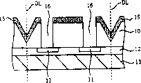
Secondly, as shown in Figure 6, by cutting along line of cut DL, dividing semiconductor substrate 10 and other each layer are finished the semiconductor device 1 that is made of semiconductor chip 10A and other each layer.At this,, form end from its semiconductor chip 10A to laterally inclined inclined plane 1s at the back side of this semiconductor device 1.
Secondly, with reference to description of drawings above-mentioned semiconductor device 1 is installed in situation on the circuitry substrate.Fig. 7 is the profile of the semiconductor device of the explanation embodiment of the invention.Both sections when Fig. 7 represents that semiconductor device 1 is connected on the circuitry substrate 30 such as printed substrate for example.In addition, on circuitry substrate 30, be formed with not shown conductive pattern.
As shown in Figure 7, semiconductor device 1 mounting makes surface (promptly being formed with the interarea of a side of the not shown conductive pattern) subtend of its back side (promptly being formed with the interarea of conducting terminal 21 sides) and circuitry substrate 80 on circuitry substrate 30.
At this, in the surface of the circuitry substrate 30 that forms not shown conductive pattern, in the position that joins with conducting terminal 21 by print process formation for example by the conductive paste or the conductivity scolder (being expressed as conductive paste 40a, 40b after the reflow treatment described later) of for example scolding tin or silver formations such as (Ag).
Connect semiconductor device 1 and circuitry substrate 30 for being situated between by above-mentioned conductive paste, carry out reflow treatment (being heat treatment).It is mobile to the surface direction of semiconductor device 1 along this inclined plane 1s by the surface tension of the inclined plane 1s (promptly forming the inclined plane 1s of wiring layer 19) at semiconductor device 1 back side to have increased mobile conductive paste 40a, 40b by this reflow treatment, simultaneously, along the horizontal direction of circuitry substrate 30 flows outside to semiconductor device 1.Thus, not only conducting terminal 21, and inclined plane 1s is also covered by conductive paste 40a, 40b.The bad connection that therefore, can suppress being seen conducting terminal of conventional example and circuitry substrate to greatest extent.In addition, the mechanical strength in the time of can improving semiconductor device and be connected on the circuitry substrate.
When correctly having carried out above-mentioned connection,, there is the conductive paste 40a that overflows from the side of semiconductor device, promptly so-called side filler rod from the surface of semiconductor device 1.Therefore, the user who carries out the semiconductor device 1 of above-mentioned connection can confirm whether correctly to have carried out above-mentioned connection by observing having or not of this side filler rod.
In addition, because the surface tension of top incline 1s, conductive paste 40a, 40b have the tendency that flows towards semiconductor device 1 outside direction along circuitry substrate 30, even so compare with conventional example, on circuitry substrate 30, form a large amount of conductive pastes, also can suppress the space of 21 of adjacent conductive terminals to greatest extent and be imbedded by conductive paste 40b.That is, can suppress 21 short circuits of conducting terminal to greatest extent.
Because the mechanical strength in the time of can improving semiconductor device 1 and be connected on the circuitry substrate 30, and avoid the short circuit of 21 of conducting terminals to greatest extent, so can omit the formation operation of the underfilling 91 that the user of the being seen semiconductor device of conventional example carries out.
The result can not make complex procedures and intensity and precision when improving semiconductor device and installing.
In other words, in semiconductor device shown in Figure 71, also can cover this back side or the not shown protective layer of wiring layer 19 formation at the back side except that the end of semiconductor chip 10A.In this case, can further improve the reliability of semiconductor device.
In addition, in above-mentioned present embodiment, be formed with conducting terminal 21 at the back side of semiconductor device 10A, but the invention is not restricted to this.That is, the present invention then also can be applied to not be formed with the semiconductor device of conducting terminal 21 so long as form to connect the embedded electrode 18 of semiconductor chip and be connected with it and extend to the semiconductor device of the wiring layer 19 of inclined plane 1s.At this moment, for example as shown in Figure 8,, cover on the embedded electrode 18 and inclined plane 1s, on the wiring layer 19 that does not have conducting terminal, form conductive paste 40a, the 40b that contains with identical side filler rod shown in Figure 7 in the end of the semiconductor chip 10A of semiconductor device 1L.
Claims (12)
1. semiconductor device, its mounting is characterized in that on circuitry substrate, comprising: semiconductor chip; Pad electrode, it is formed on the surface of described semiconductor chip; The inclined plane, it is laterally inclined to this semiconductor chip from described semiconductor chip backside end; Through hole, it penetrates into the surface of described pad electrode from described semiconductor chip backside; Dielectric film, it is formed on the sidewall of described through hole and the described semiconductor chip backside except that described through hole; Embedded electrode, it is formed in the described through hole via described dielectric film, and is electrically connected with described pad electrode; Wiring layer, it is formed on via described dielectric film and contains described through hole on interior described semiconductor chip backside, be connected with described embedded electrode, and extend on the described inclined plane of described semiconductor chip, described semiconductor device makes this circuitry substrate and mounting relative with described semiconductor chip backside on described circuitry substrate.
2. semiconductor device as claimed in claim 1 is characterized in that, described embedded electrode and described wiring layer are by forming with one deck.
3. semiconductor device as claimed in claim 1 or 2 is characterized in that, has the conducting terminal that is formed on the described wiring layer.
4. semiconductor device as claimed in claim 1 or 2 is characterized in that, the conductivity filler rod that the described wiring layer on the end at the described semiconductor chip back side is formed with described embedded electrode and on the described inclined plane covers.
5. semiconductor device as claimed in claim 3 is characterized in that, forms the conductivity filler rod that covers the described wiring layer on described conducting terminal and the described inclined plane in the end at the described semiconductor chip back side.
6. semiconductor device as claimed in claim 1 or 2 is characterized in that, is formed with supporting mass on the surface of described semiconductor chip.
7. the manufacture method of a semiconductor device, it is characterized in that, comprising: prepare to distinguish, and be formed with the Semiconductor substrate of pad electrode from the teeth outwards by line of cut, at the back side of described Semiconductor substrate, form the operation of the groove that the surface direction to described Semiconductor substrate comes to a point along described line of cut; Formation arrives the operation of through hole of the described pad electrode side surface of described Semiconductor substrate from the back side of described Semiconductor substrate; The operation of formation dielectric film in described groove and on the back side of the sidewall of described through hole and the described Semiconductor substrate except that described through hole; Formation is arranged in the described through hole and the operation of the embedded electrode that is electrically connected with described pad electrode via described dielectric film; Formation is configured in via described dielectric film and contains described through hole in the operation that is connected and extends near the wiring layer the described line of cut on the interior described semiconductor chip backside, with described embedded electrode; By cut the operation that described Semiconductor substrate is divided into a plurality of semiconductor chips along described line of cut.
8. the manufacture method of semiconductor device as claimed in claim 7 is characterized in that, described embedded electrode and described wiring layer are by forming with one deck.
9. as the manufacture method of claim 7 or 8 described semiconductor devices, it is characterized in that having the operation that on described wiring layer, forms conducting terminal.
10. as the manufacture method of claim 7 or 8 described semiconductor devices, it is characterized in that having on described semiconductor chip backside end forms described embedded electrode and the operation of the conductivity filler rod of the described wiring layer covering on the described inclined plane.
11. the manufacture method of semiconductor device as claimed in claim 9 is characterized in that, has the operation that forms the conductivity filler rod that covers the described wiring layer on described conducting terminal and the described inclined plane in described semiconductor chip backside end.
12. the manufacture method as claim 7 or 8 described semiconductor devices is characterized in that, has preparing to form the operation of supporting mass by after the line of cut differentiation and being formed with the Semiconductor substrate of pad electrode on the surface of described semiconductor chip.
Applications Claiming Priority (2)
| Application Number | Priority Date | Filing Date | Title |
|---|---|---|---|
| JP2004152736 | 2004-05-24 | ||
| JP152736/04 | 2004-05-24 |
Publications (2)
| Publication Number | Publication Date |
|---|---|
| CN1702853A CN1702853A (en) | 2005-11-30 |
| CN100401503C true CN100401503C (en) | 2008-07-09 |
Family
ID=35446783
Family Applications (1)
| Application Number | Title | Priority Date | Filing Date |
|---|---|---|---|
| CNB2005100738045A Expired - Fee Related CN100401503C (en) | 2004-05-24 | 2005-05-24 | Semiconductor device and manufacturing method of the same |
Country Status (4)
| Country | Link |
|---|---|
| US (1) | US7504722B2 (en) |
| KR (1) | KR100673490B1 (en) |
| CN (1) | CN100401503C (en) |
| TW (1) | TWI272683B (en) |
Cited By (1)
| Publication number | Priority date | Publication date | Assignee | Title |
|---|---|---|---|---|
| CN111696948A (en) * | 2019-03-12 | 2020-09-22 | 爱思开海力士有限公司 | Semiconductor module including printed circuit board |
Families Citing this family (25)
| Publication number | Priority date | Publication date | Assignee | Title |
|---|---|---|---|---|
| US7179740B1 (en) * | 1999-05-03 | 2007-02-20 | United Microelectronics Corporation | Integrated circuit with improved interconnect structure and process for making same |
| JP2005235860A (en) | 2004-02-17 | 2005-09-02 | Sanyo Electric Co Ltd | Semiconductor device and manufacturing method thereof |
| KR20080049807A (en) * | 2005-10-03 | 2008-06-04 | 로무 가부시키가이샤 | Semiconductor device |
| DE102006003931B3 (en) * | 2006-01-26 | 2007-08-02 | Infineon Technologies Ag | Semiconductor device with external surface mount contacts and method of making the same |
| JP4812512B2 (en) * | 2006-05-19 | 2011-11-09 | オンセミコンダクター・トレーディング・リミテッド | Manufacturing method of semiconductor device |
| US7473577B2 (en) * | 2006-08-11 | 2009-01-06 | International Business Machines Corporation | Integrated chip carrier with compliant interconnect |
| US7749882B2 (en) * | 2006-08-23 | 2010-07-06 | Micron Technology, Inc. | Packaged microelectronic devices and methods for manufacturing packaged microelectronic devices |
| US8841759B2 (en) * | 2006-12-23 | 2014-09-23 | Lg Innotek Co., Ltd. | Semiconductor package and manufacturing method thereof |
| KR101382706B1 (en) * | 2007-01-30 | 2014-04-08 | 엘지이노텍 주식회사 | Stack-type semiconductor package |
| US7666711B2 (en) * | 2008-05-27 | 2010-02-23 | Stats Chippac, Ltd. | Semiconductor device and method of forming double-sided through vias in saw streets |
| JP2010103300A (en) * | 2008-10-23 | 2010-05-06 | Sanyo Electric Co Ltd | Semiconductor device, and method of manufacturing the same |
| JP5395446B2 (en) * | 2009-01-22 | 2014-01-22 | ルネサスエレクトロニクス株式会社 | Semiconductor device and manufacturing method of semiconductor device |
| US10163766B2 (en) * | 2016-11-21 | 2018-12-25 | Semiconductor Components Industries, Llc | Methods of forming leadless semiconductor packages with plated leadframes and wettable flanks |
| US8283193B2 (en) * | 2009-08-14 | 2012-10-09 | Globalfoundries Singapore Pte. Ltd. | Integrated circuit system with sealring and method of manufacture thereof |
| US8093090B1 (en) * | 2009-10-12 | 2012-01-10 | Micron Technology, Inc. | Integrated circuit edge and method to fabricate the same |
| EP2405468A1 (en) * | 2010-07-05 | 2012-01-11 | ATOTECH Deutschland GmbH | Method to form solder deposits on substrates |
| KR101688006B1 (en) * | 2010-11-26 | 2016-12-20 | 삼성전자주식회사 | Semiconductor devices |
| DE102011080929B4 (en) * | 2011-08-12 | 2014-07-17 | Infineon Technologies Ag | Process for producing a composite and a power semiconductor module |
| US8552548B1 (en) | 2011-11-29 | 2013-10-08 | Amkor Technology, Inc. | Conductive pad on protruding through electrode semiconductor device |
| JP2016157880A (en) * | 2015-02-26 | 2016-09-01 | ルネサスエレクトロニクス株式会社 | Method of manufacturing semiconductor device, and semiconductor device |
| US10121742B2 (en) | 2017-03-15 | 2018-11-06 | Amkor Technology, Inc. | Method of forming a packaged semiconductor device using ganged conductive connective assembly and structure |
| US10290512B2 (en) | 2017-05-17 | 2019-05-14 | Nanya Technology Corporation | Semiconductor structure having bump on tilting upper corner surface |
| US10199312B1 (en) | 2017-09-09 | 2019-02-05 | Amkor Technology, Inc. | Method of forming a packaged semiconductor device having enhanced wettable flank and structure |
| US10366943B2 (en) | 2017-09-16 | 2019-07-30 | Amkor Technology, Inc. | Packaged electronic device having stepped conductive structure and related methods |
| KR102525161B1 (en) | 2018-07-16 | 2023-04-24 | 삼성전자주식회사 | Semiconductor device and semiconductor package comprising the same |
Citations (5)
| Publication number | Priority date | Publication date | Assignee | Title |
|---|---|---|---|---|
| CN1179009A (en) * | 1996-10-04 | 1998-04-15 | Lg半导体株式会社 | Semiconductor packaging and its socket |
| US5901046A (en) * | 1996-12-10 | 1999-05-04 | Denso Corporation | Surface mount type package unit and method for manufacturing the same |
| US6235554B1 (en) * | 1995-11-27 | 2001-05-22 | Micron Technology, Inc. | Method for fabricating stackable chip scale semiconductor package |
| US20010053567A1 (en) * | 1999-02-16 | 2001-12-20 | Salman Akram | Method of forming a test insert for interfacing a device containing contact bumps with a test substrate |
| US20020063332A1 (en) * | 2000-09-19 | 2002-05-30 | Yoshihide Yamaguchi | Semiconductor device and method for manufacturing the same and semiconductor device-mounted structure |
Family Cites Families (19)
| Publication number | Priority date | Publication date | Assignee | Title |
|---|---|---|---|---|
| US4862247A (en) * | 1987-11-24 | 1989-08-29 | Texas Instruments Incorporated | Contact joint for semiconductor chip carriers |
| US5973396A (en) * | 1996-02-16 | 1999-10-26 | Micron Technology, Inc. | Surface mount IC using silicon vias in an area array format or same size as die array |
| IL123207A0 (en) | 1998-02-06 | 1998-09-24 | Shellcase Ltd | Integrated circuit device |
| US6624505B2 (en) * | 1998-02-06 | 2003-09-23 | Shellcase, Ltd. | Packaged integrated circuits and methods of producing thereof |
| JP3497722B2 (en) | 1998-02-27 | 2004-02-16 | 富士通株式会社 | Semiconductor device, method of manufacturing the same, and transfer tray thereof |
| US5969461A (en) * | 1998-04-08 | 1999-10-19 | Cts Corporation | Surface acoustic wave device package and method |
| JP3677429B2 (en) | 2000-03-09 | 2005-08-03 | Necエレクトロニクス株式会社 | Method of manufacturing flip chip type semiconductor device |
| JP4020367B2 (en) * | 2001-04-17 | 2007-12-12 | 株式会社ルネサステクノロジ | Manufacturing method of semiconductor device |
| US6861757B2 (en) * | 2001-09-03 | 2005-03-01 | Nec Corporation | Interconnecting substrate for carrying semiconductor device, method of producing thereof and package of semiconductor device |
| US6552529B1 (en) * | 2001-12-17 | 2003-04-22 | International Business Machines Corporation | Method and apparatus for interim assembly electrical testing of circuit boards |
| JP2003229518A (en) | 2002-02-05 | 2003-08-15 | Sanyo Electric Co Ltd | Circuit device |
| JP4212293B2 (en) | 2002-04-15 | 2009-01-21 | 三洋電機株式会社 | Manufacturing method of semiconductor device |
| TWI232560B (en) * | 2002-04-23 | 2005-05-11 | Sanyo Electric Co | Semiconductor device and its manufacture |
| TWI227050B (en) * | 2002-10-11 | 2005-01-21 | Sanyo Electric Co | Semiconductor device and method for manufacturing the same |
| SG137651A1 (en) * | 2003-03-14 | 2007-12-28 | Micron Technology Inc | Microelectronic devices and methods for packaging microelectronic devices |
| JP4130158B2 (en) * | 2003-06-09 | 2008-08-06 | 三洋電機株式会社 | Semiconductor device manufacturing method, semiconductor device |
| JP4307284B2 (en) * | 2004-02-17 | 2009-08-05 | 三洋電機株式会社 | Manufacturing method of semiconductor device |
| US7129114B2 (en) * | 2004-03-10 | 2006-10-31 | Micron Technology, Inc. | Methods relating to singulating semiconductor wafers and wafer scale assemblies |
| JP4746847B2 (en) * | 2004-04-27 | 2011-08-10 | 三洋電機株式会社 | Manufacturing method of semiconductor device |
-
2005
- 2005-04-26 TW TW094113194A patent/TWI272683B/en not_active IP Right Cessation
- 2005-05-23 KR KR1020050042822A patent/KR100673490B1/en not_active IP Right Cessation
- 2005-05-24 US US11/135,668 patent/US7504722B2/en active Active
- 2005-05-24 CN CNB2005100738045A patent/CN100401503C/en not_active Expired - Fee Related
Patent Citations (5)
| Publication number | Priority date | Publication date | Assignee | Title |
|---|---|---|---|---|
| US6235554B1 (en) * | 1995-11-27 | 2001-05-22 | Micron Technology, Inc. | Method for fabricating stackable chip scale semiconductor package |
| CN1179009A (en) * | 1996-10-04 | 1998-04-15 | Lg半导体株式会社 | Semiconductor packaging and its socket |
| US5901046A (en) * | 1996-12-10 | 1999-05-04 | Denso Corporation | Surface mount type package unit and method for manufacturing the same |
| US20010053567A1 (en) * | 1999-02-16 | 2001-12-20 | Salman Akram | Method of forming a test insert for interfacing a device containing contact bumps with a test substrate |
| US20020063332A1 (en) * | 2000-09-19 | 2002-05-30 | Yoshihide Yamaguchi | Semiconductor device and method for manufacturing the same and semiconductor device-mounted structure |
Cited By (1)
| Publication number | Priority date | Publication date | Assignee | Title |
|---|---|---|---|---|
| CN111696948A (en) * | 2019-03-12 | 2020-09-22 | 爱思开海力士有限公司 | Semiconductor module including printed circuit board |
Also Published As
| Publication number | Publication date |
|---|---|
| TWI272683B (en) | 2007-02-01 |
| KR100673490B1 (en) | 2007-01-24 |
| KR20060048058A (en) | 2006-05-18 |
| US20050269696A1 (en) | 2005-12-08 |
| CN1702853A (en) | 2005-11-30 |
| US7504722B2 (en) | 2009-03-17 |
| TW200608498A (en) | 2006-03-01 |
Similar Documents
| Publication | Publication Date | Title |
|---|---|---|
| CN100401503C (en) | Semiconductor device and manufacturing method of the same | |
| KR100671921B1 (en) | Semiconductor device and manufacturing method thereof | |
| US8252630B2 (en) | Semiconductor device, method of manufacturing the semiconductor device, flip chip package having the semiconductor device and method of manufacturing the flip chip package | |
| US7485967B2 (en) | Semiconductor device with via hole for electric connection | |
| CN100383938C (en) | Semiconductor device and manufacturing method thereof | |
| US9799592B2 (en) | Semicondutor device with through-silicon via-less deep wells | |
| US7858443B2 (en) | Leadless integrated circuit package having standoff contacts and die attach pad | |
| CN102543923B (en) | Semiconductor device and manufacture method thereof | |
| US6787392B2 (en) | Structure and method of direct chip attach | |
| KR100608184B1 (en) | Semiconductor device and method for manufacturing the same | |
| WO2003063248A1 (en) | Semiconductor die package with semiconductor die having side electrical connection | |
| US20040136123A1 (en) | Circuit devices and method for manufacturing the same | |
| US11646248B2 (en) | Semiconductor device having a lead flank and method of manufacturing a semiconductor device having a lead flank | |
| US10109564B2 (en) | Wafer level chip scale semiconductor package | |
| KR100787892B1 (en) | Semiconductor package and methods of manufacturing the same | |
| JP2006228897A (en) | Semiconductor device | |
| JP4544902B2 (en) | Semiconductor device and manufacturing method thereof | |
| JP2005311117A (en) | Semiconductor device and its manufacturing method | |
| JP4518995B2 (en) | Semiconductor device and manufacturing method thereof | |
| JP4845986B2 (en) | Semiconductor device | |
| KR20010004041A (en) | method of fabricating chip size package | |
| JP2007142143A (en) | Semiconductor device and manufacturing method thereof | |
| JP2005072223A (en) | Semiconductor device |
Legal Events
| Date | Code | Title | Description |
|---|---|---|---|
| C06 | Publication | ||
| PB01 | Publication | ||
| C10 | Entry into substantive examination | ||
| SE01 | Entry into force of request for substantive examination | ||
| C14 | Grant of patent or utility model | ||
| GR01 | Patent grant | ||
| CF01 | Termination of patent right due to non-payment of annual fee |
Granted publication date: 20080709 Termination date: 20210524 |
|
| CF01 | Termination of patent right due to non-payment of annual fee |