CN100409087C - TFT array substrate and active array addressing LCD device - Google Patents
TFT array substrate and active array addressing LCD device Download PDFInfo
- Publication number
- CN100409087C CN100409087C CNB021277796A CN02127779A CN100409087C CN 100409087 C CN100409087 C CN 100409087C CN B021277796 A CNB021277796 A CN B021277796A CN 02127779 A CN02127779 A CN 02127779A CN 100409087 C CN100409087 C CN 100409087C
- Authority
- CN
- China
- Prior art keywords
- tft
- light shield
- layer
- shield layer
- substrate
- Prior art date
- Legal status (The legal status is an assumption and is not a legal conclusion. Google has not performed a legal analysis and makes no representation as to the accuracy of the status listed.)
- Expired - Lifetime
Links
- 239000000758 substrate Substances 0.000 title claims abstract description 150
- 239000011159 matrix material Substances 0.000 claims abstract description 193
- 230000008033 biological extinction Effects 0.000 claims description 17
- 239000012535 impurity Substances 0.000 claims description 14
- 239000000463 material Substances 0.000 claims description 13
- 229910052710 silicon Inorganic materials 0.000 claims description 13
- 239000010703 silicon Substances 0.000 claims description 13
- 239000004973 liquid crystal related substance Substances 0.000 claims description 7
- 239000010410 layer Substances 0.000 description 538
- 239000011229 interlayer Substances 0.000 description 46
- 229910021420 polycrystalline silicon Inorganic materials 0.000 description 40
- 229920005591 polysilicon Polymers 0.000 description 39
- 230000008901 benefit Effects 0.000 description 35
- 229910021417 amorphous silicon Inorganic materials 0.000 description 32
- 229910004298 SiO 2 Inorganic materials 0.000 description 26
- 238000000034 method Methods 0.000 description 26
- 230000000694 effects Effects 0.000 description 21
- 239000012212 insulator Substances 0.000 description 17
- 238000005516 engineering process Methods 0.000 description 16
- XUIMIQQOPSSXEZ-UHFFFAOYSA-N Silicon Chemical compound [Si] XUIMIQQOPSSXEZ-UHFFFAOYSA-N 0.000 description 9
- 238000001259 photo etching Methods 0.000 description 9
- 230000015572 biosynthetic process Effects 0.000 description 7
- 238000004519 manufacturing process Methods 0.000 description 7
- 238000005286 illumination Methods 0.000 description 6
- 230000001902 propagating effect Effects 0.000 description 6
- 239000011651 chromium Substances 0.000 description 5
- 238000002425 crystallisation Methods 0.000 description 5
- 230000008025 crystallization Effects 0.000 description 5
- 238000000151 deposition Methods 0.000 description 5
- 238000005224 laser annealing Methods 0.000 description 5
- 229910021332 silicide Inorganic materials 0.000 description 5
- FVBUAEGBCNSCDD-UHFFFAOYSA-N silicide(4-) Chemical compound [Si-4] FVBUAEGBCNSCDD-UHFFFAOYSA-N 0.000 description 5
- VYPSYNLAJGMNEJ-UHFFFAOYSA-N Silicium dioxide Chemical compound O=[Si]=O VYPSYNLAJGMNEJ-UHFFFAOYSA-N 0.000 description 4
- 230000008021 deposition Effects 0.000 description 4
- 239000003550 marker Substances 0.000 description 4
- 230000005855 radiation Effects 0.000 description 4
- 230000003595 spectral effect Effects 0.000 description 4
- 230000008859 change Effects 0.000 description 3
- 230000006872 improvement Effects 0.000 description 3
- 238000004518 low pressure chemical vapour deposition Methods 0.000 description 3
- 238000010521 absorption reaction Methods 0.000 description 2
- 239000004411 aluminium Substances 0.000 description 2
- 229910052782 aluminium Inorganic materials 0.000 description 2
- XAGFODPZIPBFFR-UHFFFAOYSA-N aluminium Chemical compound [Al] XAGFODPZIPBFFR-UHFFFAOYSA-N 0.000 description 2
- 230000033228 biological regulation Effects 0.000 description 2
- MRNHPUHPBOKKQT-UHFFFAOYSA-N indium;tin;hydrate Chemical compound O.[In].[Sn] MRNHPUHPBOKKQT-UHFFFAOYSA-N 0.000 description 2
- 239000000203 mixture Substances 0.000 description 2
- 230000003287 optical effect Effects 0.000 description 2
- 238000000623 plasma-assisted chemical vapour deposition Methods 0.000 description 2
- 230000001105 regulatory effect Effects 0.000 description 2
- 239000004065 semiconductor Substances 0.000 description 2
- 239000000377 silicon dioxide Substances 0.000 description 2
- 235000012239 silicon dioxide Nutrition 0.000 description 2
- 239000002210 silicon-based material Substances 0.000 description 2
- 238000004544 sputter deposition Methods 0.000 description 2
- 230000009897 systematic effect Effects 0.000 description 2
- 238000002834 transmittance Methods 0.000 description 2
- WQJQOUPTWCFRMM-UHFFFAOYSA-N tungsten disilicide Chemical compound [Si]#[W]#[Si] WQJQOUPTWCFRMM-UHFFFAOYSA-N 0.000 description 2
- 229910021342 tungsten silicide Inorganic materials 0.000 description 2
- VYZAMTAEIAYCRO-UHFFFAOYSA-N Chromium Chemical compound [Cr] VYZAMTAEIAYCRO-UHFFFAOYSA-N 0.000 description 1
- 230000003321 amplification Effects 0.000 description 1
- 238000000137 annealing Methods 0.000 description 1
- 229910052804 chromium Inorganic materials 0.000 description 1
- 229910052681 coesite Inorganic materials 0.000 description 1
- 238000001816 cooling Methods 0.000 description 1
- 238000010168 coupling process Methods 0.000 description 1
- 229910052906 cristobalite Inorganic materials 0.000 description 1
- 230000002950 deficient Effects 0.000 description 1
- 239000002019 doping agent Substances 0.000 description 1
- 230000005684 electric field Effects 0.000 description 1
- 230000005284 excitation Effects 0.000 description 1
- 230000005669 field effect Effects 0.000 description 1
- 239000011521 glass Substances 0.000 description 1
- 230000003760 hair shine Effects 0.000 description 1
- 238000010438 heat treatment Methods 0.000 description 1
- 229910001385 heavy metal Inorganic materials 0.000 description 1
- 230000005764 inhibitory process Effects 0.000 description 1
- 238000009413 insulation Methods 0.000 description 1
- 239000012774 insulation material Substances 0.000 description 1
- 230000007257 malfunction Effects 0.000 description 1
- 239000013081 microcrystal Substances 0.000 description 1
- 230000004048 modification Effects 0.000 description 1
- 238000012986 modification Methods 0.000 description 1
- 238000003199 nucleic acid amplification method Methods 0.000 description 1
- 230000000149 penetrating effect Effects 0.000 description 1
- 229920002120 photoresistant polymer Polymers 0.000 description 1
- 230000008569 process Effects 0.000 description 1
- 230000009467 reduction Effects 0.000 description 1
- 230000004044 response Effects 0.000 description 1
- 230000000630 rising effect Effects 0.000 description 1
- 238000005389 semiconductor device fabrication Methods 0.000 description 1
- 229910052682 stishovite Inorganic materials 0.000 description 1
- 239000000126 substance Substances 0.000 description 1
- 239000010409 thin film Substances 0.000 description 1
- 229910052905 tridymite Inorganic materials 0.000 description 1
- 230000000007 visual effect Effects 0.000 description 1
Images


Classifications
-
- H—ELECTRICITY
- H01—ELECTRIC ELEMENTS
- H01L—SEMICONDUCTOR DEVICES NOT COVERED BY CLASS H10
- H01L29/00—Semiconductor devices adapted for rectifying, amplifying, oscillating or switching, or capacitors or resistors with at least one potential-jump barrier or surface barrier, e.g. PN junction depletion layer or carrier concentration layer; Details of semiconductor bodies or of electrodes thereof ; Multistep manufacturing processes therefor
- H01L29/66—Types of semiconductor device ; Multistep manufacturing processes therefor
- H01L29/68—Types of semiconductor device ; Multistep manufacturing processes therefor controllable by only the electric current supplied, or only the electric potential applied, to an electrode which does not carry the current to be rectified, amplified or switched
- H01L29/76—Unipolar devices, e.g. field effect transistors
- H01L29/772—Field effect transistors
- H01L29/78—Field effect transistors with field effect produced by an insulated gate
- H01L29/786—Thin film transistors, i.e. transistors with a channel being at least partly a thin film
- H01L29/78606—Thin film transistors, i.e. transistors with a channel being at least partly a thin film with supplementary region or layer in the thin film or in the insulated bulk substrate supporting it for controlling or increasing the safety of the device
- H01L29/78633—Thin film transistors, i.e. transistors with a channel being at least partly a thin film with supplementary region or layer in the thin film or in the insulated bulk substrate supporting it for controlling or increasing the safety of the device with a light shield
-
- G—PHYSICS
- G02—OPTICS
- G02F—OPTICAL DEVICES OR ARRANGEMENTS FOR THE CONTROL OF LIGHT BY MODIFICATION OF THE OPTICAL PROPERTIES OF THE MEDIA OF THE ELEMENTS INVOLVED THEREIN; NON-LINEAR OPTICS; FREQUENCY-CHANGING OF LIGHT; OPTICAL LOGIC ELEMENTS; OPTICAL ANALOGUE/DIGITAL CONVERTERS
- G02F1/00—Devices or arrangements for the control of the intensity, colour, phase, polarisation or direction of light arriving from an independent light source, e.g. switching, gating or modulating; Non-linear optics
- G02F1/01—Devices or arrangements for the control of the intensity, colour, phase, polarisation or direction of light arriving from an independent light source, e.g. switching, gating or modulating; Non-linear optics for the control of the intensity, phase, polarisation or colour
- G02F1/13—Devices or arrangements for the control of the intensity, colour, phase, polarisation or direction of light arriving from an independent light source, e.g. switching, gating or modulating; Non-linear optics for the control of the intensity, phase, polarisation or colour based on liquid crystals, e.g. single liquid crystal display cells
- G02F1/133—Constructional arrangements; Operation of liquid crystal cells; Circuit arrangements
- G02F1/136—Liquid crystal cells structurally associated with a semi-conducting layer or substrate, e.g. cells forming part of an integrated circuit
- G02F1/1362—Active matrix addressed cells
- G02F1/136209—Light shielding layers, e.g. black matrix, incorporated in the active matrix substrate, e.g. structurally associated with the switching element
-
- H—ELECTRICITY
- H01—ELECTRIC ELEMENTS
- H01L—SEMICONDUCTOR DEVICES NOT COVERED BY CLASS H10
- H01L27/00—Devices consisting of a plurality of semiconductor or other solid-state components formed in or on a common substrate
- H01L27/02—Devices consisting of a plurality of semiconductor or other solid-state components formed in or on a common substrate including semiconductor components specially adapted for rectifying, oscillating, amplifying or switching and having at least one potential-jump barrier or surface barrier; including integrated passive circuit elements with at least one potential-jump barrier or surface barrier
- H01L27/12—Devices consisting of a plurality of semiconductor or other solid-state components formed in or on a common substrate including semiconductor components specially adapted for rectifying, oscillating, amplifying or switching and having at least one potential-jump barrier or surface barrier; including integrated passive circuit elements with at least one potential-jump barrier or surface barrier the substrate being other than a semiconductor body, e.g. an insulating body
-
- G—PHYSICS
- G02—OPTICS
- G02F—OPTICAL DEVICES OR ARRANGEMENTS FOR THE CONTROL OF LIGHT BY MODIFICATION OF THE OPTICAL PROPERTIES OF THE MEDIA OF THE ELEMENTS INVOLVED THEREIN; NON-LINEAR OPTICS; FREQUENCY-CHANGING OF LIGHT; OPTICAL LOGIC ELEMENTS; OPTICAL ANALOGUE/DIGITAL CONVERTERS
- G02F1/00—Devices or arrangements for the control of the intensity, colour, phase, polarisation or direction of light arriving from an independent light source, e.g. switching, gating or modulating; Non-linear optics
- G02F1/01—Devices or arrangements for the control of the intensity, colour, phase, polarisation or direction of light arriving from an independent light source, e.g. switching, gating or modulating; Non-linear optics for the control of the intensity, phase, polarisation or colour
- G02F1/13—Devices or arrangements for the control of the intensity, colour, phase, polarisation or direction of light arriving from an independent light source, e.g. switching, gating or modulating; Non-linear optics for the control of the intensity, phase, polarisation or colour based on liquid crystals, e.g. single liquid crystal display cells
- G02F1/133—Constructional arrangements; Operation of liquid crystal cells; Circuit arrangements
- G02F1/136—Liquid crystal cells structurally associated with a semi-conducting layer or substrate, e.g. cells forming part of an integrated circuit
- G02F1/1362—Active matrix addressed cells
- G02F1/136227—Through-hole connection of the pixel electrode to the active element through an insulation layer
Abstract
A TFT array substrate is provided, which effectively blocks the light traveling toward the active layers of the TFTs. A patterned first light-shielding layer is formed between a transparent plate and TFTs in such a way as to overlap with the active layers of the TFTs. A patterned third light-shielding layer is formed to cover the TFTs on the opposite side to the plate with respect to the TFTs. The third light-shielding layer has the first parts extending along the rows of the matrix and the second parts extending along the columns thereof. A patterned second light-shielding layer is formed between the first light-shielding layer and the TFTs. The second light-shielding layer has a light-absorbing property, which absorbs the light entering the inside of the substrate. A patterned fourth light-shielding layer, which has a light-absorbing property, may be additionally provided between the TFTs and the third light-shielding layer.
Description
Technical field
The present invention relates generally to liquid crystal display (LCD) device.Particularly, the present invention relates to form arrangement thereon a kind of substrate of thin film transistor (TFT) (TET), i.e. TFT matrix basis, and a kind of active array addressing LCD device that is equipped with this substrate with matrix array.The lighting bulb that preferably this substrate and equipment is used for projection type display device.
Background technology
In recent years, developed the various display device that is applicable to wall-hanging TV (TV), projection type TV or office automation (OA) equipment.For realizing being used for OA equipment or high-definition television high-grade display devices such as (HDTV), wish day by day in traditional display device, use the active array addressing LCD device as its on-off element with TFT.This is because active-matrix LCD device has an advantage: even if the number of sweep trace increases, its contrast and response speed can not reduce yet.In addition, active-matrix LCD device also has another advantage: if with they lighting bulbs as projection type display device, then be easy to realize the large scale display screen.
For the LCD device that is exclusively used in lighting bulb, in general, high-luminance light afterwards, according to picture information, is controlled the light of such input from light source input LCD device, and simultaneously, light passes same equipment.In other words, in drive TFT, by electric field being applied to the transmissivity that changes each pixel on each pixel, thereby regulate the light intensity that penetrates this equipment.Afterwards, utilize the projected light system that comprises special-purpose lens, will pass the light amplification of this device, and project on the giant-screen.
Light source is positioned on the opposed base side of LCD device, and the projected light system is positioned at TFT matrix basis one side.Like this, be not only the light that goes out from light emitted, and also will enter this device by the light that the projected light systematic reflection returns.
For active array addressing LCD device, resemble the active layer that a such semiconductor layer of amorphous silicon or polysilicon (i.e. semiconductor layer) is used to each TFT.If illumination is mapped on the active layer, can cause owing to optical excitation that then electric current leaks.On the other hand, as previously mentioned, high-luminance light is used for lighting bulb by defeated LCD device, and like this, electric current leaks will become big.Because except the light from light source, the light that is returned by the projected light systematic reflection also shines on the active layer, electric current leaks and becomes big probably.
In recent years, a kind of trend is arranged, promptly projection type LCD device is designed to be more and more compacter, and has higher brightness.Like this, the brightness that is input to the light in the device becomes more and more higher.From this point, the problems referred to above that relevant electric current leaks will become more serious.For addressing this problem, utilize existing active array addressing LCD device, as lighting bulb, need provide light shield layer, to prevent that rayed is to the active layer of TFT.
Fig. 1 and Fig. 2 A and 2B show the schematic structure of the TFT matrix basis 100 of such existing LCD device, wherein, for for simplicity, only show a pixel.Fig. 1 is the partial plan of substrate 100, and Fig. 2 A is the sectional view of the line IIA-IIA in Fig. 1, and Fig. 2 B is the sectional view of the line IIB-IIB in Fig. 1.Because all pixels all have identical structure, so these figure only show in these pixels.
Existing TFT matrix basis 100 comprises a transparent panel 101, and the form with matrix array on it is arranged with TFT 131.By tungsten silicide (WSi
2) light shield layer 103 of the bottom that constitutes, by means of silicon dioxide (SiO
2) layer 102 is formed on the plate 101.The flat shape of bottom light shield layer 103 is similar to grid (lattice), and it is the Cross slat that extended by the row (directions X among Fig. 1) along the matrix of TFT 131 and extends and constitute with vertical bar that Cross slat intersects along its row (the Y direction among Fig. 1).Complete layer 103 SiO who is capped thereon
2104 covering of layer.
Each polysilicon active layer 107 all comprises LDD (drain electrode of light dope) the district 107b and the 107d of a undoped channel region 107c, two light dopes, a heavy-doped source polar region 107a and a heavily doped drain region 107e.Source electrode and drain region 107a and 107e are positioned at each side of raceway groove 107c.LDD district 107b is between source area 107a and channel region 107c.LDD district 107d is between channel region 107c and drain region 107e.
By the data line 111 that aluminium (AL) is made, be formed on first interlayer insulative layer 110.These lines 111 are parallel to each other, and extend along the Y direction.Each bar to line 111 is placed, and makes its active layer 107 with the TFT 131 that belongs to the same row of matrix overlapping.Line 111 has covered source area 107a, channel region 107c and LDD district 107b and the 107d of corresponding TFT 131 fully.Line 111 has covered the part drain region 107e of corresponding TFT 131.By connecting the contact hole 121 of first interlayer insulative layer 110 and gate insulator 108, line 111 with belong to the source area 107a of matrix and carry out mechanical connection and be electrically connected with the TFT 131 of delegation.Line 111 is covered by second interlayer insulative layer 112 fully.
The figuratum black matrix layer 113 that forms by chromium (Cr) formation is formed on second interlayer insulative layer 112.Layer 113 flat shape is similar to grid, and it is the Cross slat that extended by the row (directions X among Fig. 1) along matrix and extends and constitute with vertical bar that Cross slat intersects along its row (the Y direction among Fig. 1).Layer 113 forms pattern, so as overlapping with gate line 109 and data line 111, thus cover TFT 131.Layer 113 is as the top light shield layer.Layer 113 is covered by the 3rd interlayer insulative layer 114 fully.
Have a pixel electrode 115 that is approximately rectangular planar shape, be formed on the 3rd interlayer insulative layer 114.Electrode 115 is positioned at by gate line 109 and data line 111 determined corresponding pixel regions 120.By penetrating the contact hole 122 of the 3rd interlayer insulative layer 114, second interlayer insulative layer 112, first interlayer insulative layer 110 and gate insulator 108, the drain region 107e of electrode 115 and corresponding TFT 131 carries out mechanical connection and is electrically connected.
Utilization comprises the existing LCD device of the existing TFT matrix basis 100 with said structure, and opposed substrate (not shown) and substrate 100 are coupled, so that between these two substrates, form a liquid crystal layer.Enter the light of LCD device from a side of opposed substrate, stopped by black matrix layer (being the top light shield layer) 113.The light that enters from TFT matrix basis 100 1 sides is stopped by bottom light shield layer 103.But, a problem is arranged here, promptly can not prevent fully from the illumination that substrate 100 1 sides enter be mapped to the LDD district 107b of TFT 131 and 107b with and/or channel region 107c.Below, will this situation be elaborated referring to Fig. 3.
As shown in Figure 3, enter the light L101 of LCD device, stopped by black matrix layer (being the top light shield layer) 113 from opposed substrate one side.Another kind of scheme is: light L101 passes substrate 100, and not by 103 reflections of bottom light shield layer.This is because can be for this purpose, well the interval between the width of regulating course 113 and layer 103 and layer 113 and the layer 103.The light L102 that enters the LCD device from a side of substrate 100 is stopped by bottom light shield layer 103.
But, as can from Fig. 3, seeing, from TFT matrix basis 100 1 sides enter the LCD device, towards the light L103 of black matrix layer 113, tegillum 113 reflects, and forward to the bottom light shield layer 103 on.Afterwards, light L103 is by repeatedly reflecting in the space that runs in the guide between layer 103 and the data line 111, and is last, arrives LDD district 107b.But, from substrate 100 1 sides enter the LCD device, towards the light L104 of data line 111, last by repeatedly reflecting in the space that runs in the guide between layer 103 and the data line 111, arrive LDD district 107b.Similarly, through repeatedly the reflection after, illumination is mapped to LDD district 107d.In fact, the various light that comprise light L103 and L104 enter from a side of substrate 100, and this illumination is mapped to channel region 107c.
For avoiding this problem, various improvement projects have been developed and disclose.
For example, Japan is uncensored, disclose a kind of LCD device among the disclosed patent disclosure No.2000-180899 in June, 2000, and wherein the end of bottom light shield layer is tapered, thereby forms a trapezoid cross section.In this device, if can regulate the width of bottom light shield layer and the width of data line well, just can stop the light that enters the LCD device from TFT matrix basis one side with the bottom light shield layer, like this, just prevented that irradiate light is to channel region.
Uncensored in Japan, a kind of LCD device is disclosed among the disclosed patent disclosure No.2000-356787 in Dec, 2000, wherein, in the dielectric layer that covers the bottom light shield layer, form empty contact hole in position near channel region.Filled up lead material in the empty contact hole.In this device, the lead material of inserting in the sky contact hole has stopped the light that enters the LCD device from TFT matrix basis one side, like this, has just prevented that illumination is mapped to channel region.
In addition, well-known, black matrix layer can be positioned on the TFT matrix basis or in the opposed substrate.If black matrix layer is positioned in the opposed substrate, in the coupling process of TFT matrix basis and opposed substrate, need the alignment error (being tolerance) of the about 10 μ m of forethought, simultaneously, also to consider the covering precision between these two substrates.As a result, black matrix layer must non-constant width.This caused can not the hole diameter enlargement ratio defective.
Different therewith, if black matrix layer is positioned on the TFT matrix basis, then can utilize the known semiconductor device fabrication, improve the alignment accuracy between black matrix layer and the TFT.Therefore, shown in Fig. 1,2A and 2B, this structure becomes main flow just day by day.
As mentioned above, use to have the existing LCD device of Fig. 1 and 2 A to the existing TFT matrix basis 100 of 2B, a part that enters the light of LCD device from substrate 100 1 sides arrive possibly LDD district 107b and 107d with and/or channel region 107c.Like this, the leakage of the electric current that is caused by light increases, and the result contrast occurred and descended and the uneven problem of image quality.
Utilize disclosed LCD device among the patent disclosure No.2000-180899, the processing step of the tapering point of light shield layer bottom then needing to form.Therefore, there is the manufacturing process complicated problems.
Utilize disclosed LCD device among the publication number No.2000-356787, then need form the processing step of empty contact hole near the channel region place in the insulation course that covers the bottom light shield layer, and the processing step of filling empty contact hole with lead material.Therefore, have the manufacturing process complicated problems, this is identical with problem among the publication number No.200-180899.
In addition, utilize the disclosed LCD device of publication number No.2000-180899 and 2000-356787, if these devices are used in the lighting bulb that is used for high-brightness projection escope spare, are difficult to effective reaching fully the light of propagating towards the active layer of TFT is stopped.
Summary of the invention
Therefore, an object of the present invention is to provide a kind of TFT matrix basis and a kind of LCD device, it can effectively stop the light of propagating towards the active layer of TFT.
Another object of the present invention provides a kind of TFT matrix basis and a kind of LCD device, and it can suppress the leakage of the electric current that is caused by light in the TFT.
Another object of the present invention provides a TFT matrix basis and a kind of LCD device, and it can improve the contrast and the homogeneity of image quality.
Another object of the present invention provides does not use the complicated processing step just can produced at an easy rate a kind of TFT matrix basis and a kind of LCD device.
By following explanation, can make the clear understanding of those skilled in the art above-mentioned purpose, also have other unspecified purpose simultaneously.
According to first aspect of the present invention, a kind of TFT matrix basis is provided, it comprises:
(a) transparent panel;
(b) be arranged in TFT on the described plate with the matrix array of embarking on journey into row;
Each TFT has one first source/drain regions, second source/drain regions, and an active layer;
(c) mode of extending with the row along described array is formed at the gate line on the described plate;
(d) mode of extending with the row along described array is formed at the data line on the described plate;
Each bar data line all is electrically connected with first source/drain regions of a corresponding TFT;
(e) pixel electrode is formed in the pixel region on the described plate;
Each pixel electrode all is electrically connected with second source/drain regions of a corresponding TFT;
(f) have first light shield layer of pattern, be formed in such a way between described plate and the TFT, so as with the active layer overlaid of described TFT;
(g) have second light shield layer of pattern, be formed between described first light shield layer and the described TFT;
Described second light shield layer has extinction characteristic;
(h) have the 3rd light shield layer of pattern, forming it so that cover with respect to TFT is the TFT that is positioned on the offside of described plate;
Described the 3rd light shield layer has the first of extending along the row of described matrix, and is listed as the second portion that extends along it.
According to the TFT matrix basis of first aspect present invention, first light shield layer with pattern is formed between described plate and the described TFT in such a way, so as with the active layer overlaid of TFT.Formation has the 3rd light shield layer of pattern, is the TFT that is positioned on the relative side with described plate to cover with respect to TFT.The 3rd light shield layer has the first of the row extension of prolonging matrix, and the second portion of Yan Qilie extension.In addition, second light shield layer with pattern is formed between first light shield layer and the TFT.Second light shield layer has extinction characteristic.
Therefore, both be the light that enters into TFT matrix basis inside from a side of described plate, the 3rd light shield layer with pattern with and/or data line reflect, reflected by first light shield layer again afterwards with pattern, all reflected light also all have arrival second light shield layer of pattern.Because second light shield layer has extinction characteristic, so reflected light also will be absorbed by second light shield layer.Any light that can stop like this, the active layer propagation of the TFT in the TFT matrix basis effectively.This means that active layer can not be exposed in the light.As a result, suppress the leakage of the electric current that causes by light in the TFT, therefore improved the contrast and the homogeneity of image quality.
In addition, also do not need as disclosed the sort of complicated manufacturing process among the patent publication No. No.2000-180899 of Japanese laid-open and the 2000-356787.Like this, can not use complicated technology just can produce the TFT matrix basis at an easy rate.
In the most preferred embodiment of the substrate of foundation first aspect present invention, each TFT has a channel region and a LDD district.Second light shield layer has the first of the channel region that covers TFT, and the second portion that covers its LDD district.In this embodiment, also have the another one advantage, promptly the light towards channel region and the propagation of LDD district can obtain certain stopping.Generally speaking, illumination is mapped to channel region or LDD district, will cause that electric current leaks.Like this, by stopping or suppress light, just can reduce electric current effectively and leak.
In another most preferred embodiment of the substrate of foundation first aspect present invention, second light shield layer is to be made by the material that comprises silicon.Particularly, second light shield layer is made by silicon.In this embodiment, also there is the another one advantage, can more effectively suppresses the leakage of electric current.
In the another one most preferred embodiment of the substrate of foundation first aspect present invention, second light shield layer has electric conductivity.Second light shield layer has a kind of like this structure, and it allows to use constant voltage.In this embodiment, there is a kind of additional advantage, under the current potential that can being biased in of second light shield layer is required, and can controls the characteristic of TFT.
In another most preferred embodiment of the substrate of foundation first aspect present invention, second light shield layer has electric conductivity, and is electrically connected with gate line.In this example, have a kind of additional advantage, promptly TFT has a kind of double-grid structure, and this structure has the on of improvement.
In the another one most preferred embodiment of the substrate of foundation first aspect present invention, second light shield layer is to be made of the silicon that is doped with impurity.In this embodiment, there is a kind of additional advantage, promptly can provides required conductance to second light shield layer at an easy rate.
Preferably, gate line is arranged in such a way, so as with the channel region overlaid of corresponding TFT.Gate line has the function of the grid of TFT in the part overlapping with TFT.
Preferably, be respectively each TFT that separates with gate line and form grid.Gate line is electrically connected with corresponding grid.
In another most preferred embodiment of the substrate of foundation first aspect present invention, be clipped in described second light shield layer of TFT and the dielectric between the active layer and have ranges of thicknesses from 100nm to 500nm.In this embodiment, guaranteed the interception of invention.Be more preferably, dielectric thickness is from 150nm to 300nm.In this case, improved interception of the present invention.
In the most preferred embodiment of another substrate of foundation first aspect present invention, except a picture element matrix part is provided, also provide a driving circuit section that comprises TFT, wherein TFT arranges with matrix form.Described second light shield layer is that described second light shield layer is not to provide for the TFT in the driving circuit section for the TFT in the picture element matrix part provides.In this embodiment, described second light shield layer is that described second light shield layer is not to provide for the TFT in the driving circuit section for the TFT in the picture element matrix part provides.Therefore, if in laser annealing (annealing) technology, laser radiation is to the amorphous silicon layer of the active layer that is designed to the TFT in picture element matrix part and the driving circuit section, then the heat that causes of laser will be by means of second light shield layer in the picture element matrix part, with than in driving circuit section, propagate into quickly amorphous silicon layer around.As a result, the amorphous silicon layer in the picture element matrix part changes the polysilicon layer with low-crystallinity into.This means that photic electric current leakage is further suppressed.Meanwhile, the amorphous silicon layer in the driving circuit section becomes the have high mobility polysilicon layer of (mobility).
According to a second aspect of the present invention, a kind of active array addressing LCD device is provided, it comprises:
(a) according to the TFT matrix basis of first aspect;
(b) with the opposed substrate staggered relatively of described TFT matrix basis; And
(c) be formed at a liquid crystal layer between described TFT matrix basis and the described opposed substrate.
Utilization then owing to above-mentioned same reason, can obtain those shown in the TFT matrix basis according to first aspect present invention advantages according to the active array addressing LCD device of second aspect present invention.
According to a third aspect of the present invention, another kind of TFT matrix basis is provided, it comprises:
(a) transparent panel;
(b) be arranged in some TFT on the described plate plate with the matrix array form of embarking on journey into row;
Each TFT has first source/drain regions, second source/drain regions; And active layer;
(c) be formed at some gate lines on the described plate plate in such a way, so that extend along the row of described matrix;
(d) be formed at plurality of data line on the described plate plate in such a way, so that extend along described matrix column;
Each bar data line all is electrically connected with first source/drain regions of a corresponding TFT;
(e) be formed at pixel electrode in the pixel region on the described plate plate;
Each pixel electrode all is electrically connected with second source/drain regions of a corresponding TFT;
(f) be formed at first light shield layer of the formation pattern between described plate and the described TFT in such a way, so as with the active layer overlaid of described TFT;
(g) form the 3rd light shield layer, so that cover the TFT on the offside that with respect to described TFT, is positioned at described plate with pattern;
The 3rd light shield layer has the first of extending along the row of described matrix, and is listed as the second portion that extends along it; And
(h) the 4th light shield layer of formation pattern, it is formed between described TFT and described the 3rd light shield layer;
Described the 4th light shield layer has extinction characteristic.
Utilization is according to the TFT matrix basis of third aspect present invention, and first light shield layer with pattern is formed between described plate and the described TFT in such a way, so as with the active layer overlaid of described TFT.Formation has the 3rd light shield layer of pattern, is the TFT that is positioned on the offside of described plate so that cover with respect to described TFT.The 3rd light shield layer has the first of extending along the row of matrix, and is listed as the second portion that extends along it.And the 4th light shield layer with pattern is formed between described TFT and the 3rd light shield layer.The 4th light shield layer has extinction characteristic.
Therefore, even if enter into the light of TFT matrix basis inside from described plate one side, the 3rd light shield layer with pattern with and/or the data line reflection, again under the situation by first light shield layer reflection with pattern, all reflected light also can arrive the 4th light shield layer with pattern afterwards.Because the 4th light shield layer has extinction characteristic, so reflected light will be absorbed by the 4th light shield layer.Any light that can effectively stop like this, the active layer propagation of TFT in the TFT matrix basis.This means that active layer can not be exposed among the light.As a result, photic electric current leaks and is suppressed in the TFT, thus the contrast of the image quality of Gai Shaning and homogeneity.
And, no longer need Japanese laid-open patent to disclose the manufacturing process of disclosed complexity among No.2000-180899 and the 2000-356787.Like this, can not use complicated technology and produce the TFT matrix basis at an easy rate.
In the most preferred embodiment of foundation third aspect present invention substrate, each TFT has channel region and LDD district.Second light shield layer has the first of the channel region that covers TFT, and the second portion that covers its LDD district.In this embodiment, there is another advantage, promptly stopped light really towards channel region and the propagation of LDD district.Generally speaking, the rayed to channel region or LDD district will cause that electric current leaks.Like this, by stopping or suppress light, can reduce electric current effectively and leak.
In another embodiment of the substrate of foundation third embodiment of the invention, the 4th light shield layer is to be made by the material that comprises silicon.Preferably, the 4th light shield layer is made by silicon.In this embodiment, have the another one advantage, promptly electric current leaks and obtains more effective inhibition.
In another most preferred embodiment of the substrate of foundation third aspect present invention, the 4th light shield layer has electric conductivity.The 4th light shield layer has a kind of structure that allows to apply constant voltage.In this embodiment, have another advantage, promptly the 4th light shield layer can be offset under the required electromotive force, and can control the characteristic of TFT.
In another most preferred embodiment of the substrate of foundation third aspect present invention, the 4th light shield layer has electric conductivity, and is electrically connected to described gate line.
In the another one embodiment of the substrate of foundation third aspect present invention, the 4th light shield layer is to be made of the silicon that mixes.In this embodiment, there is an attendant advantages, promptly can gives the 4th light shield layer at an easy rate with required conductance.
Preferably, gate line is set in such a way, so as with the channel region overlaid of corresponding TFT.At their lap, gate line has the gate electrode function of TFT.
Preferably, be respectively each TFT that separates with gate line and form grid.Gate line is electrically connected with corresponding grid.
In another most preferred embodiment of the substrate of foundation third aspect present invention, between first light shield layer and TFT, also additionally formed second light shield layer with pattern.Second light shield layer has extinction characteristic.In this embodiment, the light on each side of TFT is blocked, and therefore, can obtain extraordinary shaded effect.
In another most preferred embodiment of foundation third aspect present invention, be clipped in dielectric between the active layer of second light shield layer and TFT and have thickness range from 100nm to 500nm.In this embodiment, guaranteed interception of the present invention.More preferably, dielectric thickness is from 150nm to 300nm.In this case, strengthened shaded effect of the present invention.
In another embodiment of the substrate of foundation third aspect present invention, except the picture element matrix part, also provide the driving circuit section that comprises TFT, wherein TFT arranges with the form of matrix array.Second light shield layer is that second light shield layer is not to establish for the TFT in the driving circuit section for the TFT in the picture element matrix part establishes.In this embodiment, second light shield layer is that second light shield layer is not to establish for the TFT in the driving circuit section for the TFT in the picture element matrix part establishes.Therefore, in the laser annealing operation, if during the amorphous silicon layer of the active layer of the TFT of laser radiation in being used as picture element matrix part and driving circuit section, the heat that laser causes will be by second light shield layer in the picture element matrix part, with propagate into quickly than the speed in the driving circuit section amorphous silicon layer around.As a result, the amorphous silicon layer in the picture element matrix part changes the polysilicon layer that has than low-crystallinity into.This means that the electric current leakage that is caused by light further is inhibited.Meanwhile, the amorphous silicon layer in the driving circuit section is changed into the polysilicon layer with high mobility.
According to a fourth aspect of the present invention, another kind of active array addressing LCD device is provided, it comprises:
(a) according to the TFT matrix basis of the third aspect;
(b) with the opposed substrate staggered relatively of described TFT matrix basis; And
(c) be formed at liquid crystal layer between described TFT matrix basis and the opposed substrate.
Because above-mentioned identical, utilize active array addressing LCD device according to fourth aspect present invention, can obtain with according to the identical advantage of those advantages shown in the TFT matrix basis of third aspect present invention.
Description of drawings
For realization the present invention easily, below, with reference to the accompanying drawings, be described.
Fig. 1 shows the partial plan of layout of the TFT matrix basis of prior art.
Fig. 2 A is the part sectioned view of the line IIA-IIA in Fig. 1, and it shows the structure of the existing substrate among Fig. 1.
Fig. 2 B is the part sectioned view of the line IIB-IIB in Fig. 1, and it shows the structure of the existing substrate among Fig. 1.
Fig. 3 is a schematic sectional view, and it shows the effect of the light that stops the existing substrate inside that enters into Fig. 1, and it is that line IIA-IIA in Fig. 1 sees into.
Fig. 4 is a partial plan layout, and it shows the layout according to the TFT matrix basis of first embodiment of the invention.
Fig. 5 A is the part sectioned view of a line VA-VA in Fig. 4, and it shows the underlying structure of Fig. 4.
Fig. 5 B is the part sectioned view of a line VB-VB in Fig. 4, and it shows the underlying structure of Fig. 4.
Fig. 6 is a schematic sectional view, and it shows the effect that the light to the substrate inside that enters into Fig. 4 stops, it is that line VA-VA in Fig. 4 sees into.
Fig. 7 A is a part sectioned view to 11A, and they are to see into that along the line VA-VA of Fig. 4 they show the processing step of the substrate of shop drawings 4 respectively.
Fig. 7 B is a part sectioned view to 1iB, and they are that the line VB-VB in Fig. 4 sees into that they show the processing step of the substrate of shop drawings 4 respectively.
Figure 12 is a partial plan layout, and it shows the layout according to a TFT matrix basis of the second embodiment of the present invention.
Figure 13 A is the part sectioned view of a line XIIIA-XIIIA in Figure 12, and it shows the structure of the substrate of Figure 12.
Figure 13 B is the part sectioned view of a line XIIIB-XIIIB in Figure 12, and it shows the structure of the substrate of Figure 12.
Figure 14 is a partial plan layout, and it shows the layout according to a TFT matrix basis of third embodiment of the invention.
Figure 15 is a partial plan layout, and it shows the layout according to a TFT matrix basis of fourth embodiment of the invention.
Figure 16 A is the part sectioned view of a line XVIA-XVIA in Figure 15, and it shows the underlying structure of Figure 15.
Figure 16 B is the part sectioned view of a line XVIB-XVIB in Figure 15, and it shows the underlying structure of Figure 15.
Figure 17 is a schematic sectional view, and it shows the effect that the light to the substrate inside that enters into Figure 15 stops, it is that line XVIA-XVIA in Figure 15 sees into.
Figure 18 is a partial plan layout, and it shows the layout according to a TFT matrix basis of fifth embodiment of the invention.
Figure 19 is a partial plan layout, and it shows the layout according to a TFT matrix basis of sixth embodiment of the invention.
Figure 20 is a schematic sectional view, and it shows the structure of using according to the active array addressing LCD device of TFT matrix basis of the present invention.
Figure 21 A is the part sectioned view along Fig. 4 line VA-VA, and it shows the structure according to the TFT matrix basis of seventh embodiment of the invention.
Figure 21 B is the part sectioned view along Fig. 4 line VB-VB, and it shows the underlying structure of Figure 21 A.
Figure 22 A is the part sectioned view along Fig. 4 line VA-VA, and it shows the structure according to the TFT matrix basis of eighth embodiment of the invention.
Figure 22 B is the part sectioned view along Fig. 4 line VB-VB, and it shows the underlying structure of Figure 22 A.
Figure 23 A is the part sectioned view along Figure 15 line XVIA-XVIA, and it shows the structure according to the TFT matrix basis of ninth embodiment of the invention.
Figure 23 B is the part sectioned view along Figure 15 line XVIB-XVIB, and it shows the underlying structure of Figure 23 A.
Figure 24 A is the part sectioned view along Figure 15 line XVIA-XVIA, and it shows the structure according to the TFT matrix basis of tenth embodiment of the invention.
Figure 24 B is the part sectioned view along Figure 15 line XVIB-XVIB, and it shows the underlying structure of Figure 24 A.
Figure 25 shows a curve map, the relation between the thickness of the dielectric layer between the photic electric current leakage and the active layer and second light shield layer among the TFT that provides in picture element matrix part is provided for it, and this curve map is to obtain under the specific shot condition of projection light.
Figure 26 is the floor map according to the TFT matrix basis of eleventh embodiment of the invention.
Embodiment
Below, with reference to the accompanying drawings, most preferred embodiment of the present invention is elaborated.
First embodiment
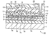
Fig. 4 and Fig. 5 A and 5B show the schematic structure according to a TFT matrix basis 30 of first embodiment of the invention, wherein, for for simplicity, only show a pixel.This situation also is applicable to any other embodiment that will illustrate after a while.
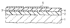
A SiO
2Layer 2 is formed on the plate 1, to cover its whole surface.Layer 2 is used to prevent that the heavy metal that is contained in the plate 1 is diffused into substrate 30 inside.
First light shield layer 3 with pattern is formed at SiO
2On the layer 2.Layer 3 flat shape is similar to grid, and it is the Cross slat 3a that is extended by the row (directions X among Fig. 4) along the matrix of TFT 31, and extend along its row (the Y direction among Fig. 4) and constitute with vertical bar 3b that Cross slat intersects.Layer 3 is (for example to be WSi by the material with enough low light transmittance
2) make.Layer 3 thickness setting be enough greatly, is used to stop that from the rear side of substrate 30 be the light that a side of slave plate 1 directly enters.Whole layer 3 by position SiO thereon
24 covering of layer.
At SiO
2On the layer 4, formed second light shield layer 5 with pattern.Layer 5 is to be made of the amorphous silicon with extinction characteristic.Layer 5 comprises the horizontal bar shaped part 5a that the row (directions X among Fig. 4) along the matrix of TFT 31 extends, and along its vertical rectangle part 5b that is listed as (the Y direction among Fig. 4) extension and intersects with lateral part 5a.Bar shaped part 5a is that equidistantly vertical (along the Y direction) places, and they are parallel to each other.Rectangle part 5b is that equidistant level (along directions X) is placed, and they are parallel to each other.Make layer 5 form an a kind of pattern, so that can be fully overlapping with first light shield layer 3 that is positioned at below it.Layer 5 is by a SiO who is formed on the SiO2 layer 4
26 covering of layer.
At SiO
2On the layer 6, formed polysilicon layer 7.Make each layer 7 form pattern, so that have a flat shape that is approximately the L character.Each layer 7 all just is positioned at below the position that gate line 9 and data line 11 intersect, and this will be described hereinafter.Layer 7 is as the active layer of each TFT 31.
The active layer 7 of each polysilicon all comprises a unadulterated channel region 7c, two slight LDD district 7b and 7d, a heavy-doped source polar region 7a and heavily doped drain region 7e that mix.Source electrode and drain region 7a and 7e are positioned at each side of channel region 7c.LDD district 7b is between source area 7a and channel region 7c.LDD district 7d is between channel region 7c and drain region 7e.
By the data line 11 that A1 makes, be formed on first interlayer insulative layer 10.These lines are parallel to each other, and extend along the Y direction.Each bar line 11 all be placed on can with the active layer 7 equitant positions of the TFT 31 of the same row that belong to described matrix on.Line 11 has covered source area 7a, channel region 7c and LDD district 7b and the 7d of corresponding TFT 31 fully.Line 11 has covered the part drain region 7e of corresponding TFT 31.Line 11 by contact hole 21 with belong to matrix with the source region 7a Mechanical Contact of the TFT 31 of delegation and be electrically connected, wherein, described contact hole 21 has penetrated first interlayer insulative layer 10 and gate insulator 8.Line 11 is covered by second interlayer insulative layer 12 fully.
The black matrix layer with pattern 13 that is made of Cr is formed on second interlayer insulative layer 12.Layer 13 flat shape is similar to grid, and it is the Cross slat that extended by the row (directions X among Fig. 4) along matrix and extends and form with vertical bar that described Cross slat intersects along its row (the Y direction among Fig. 4).Make layer 13 form patterns, so as with gate line 9 and data line 11 overlaids, thereby cover TFT 31.Layer 13 is as the 3rd light shield layer.One the 3rd interlayer insulative layer 14 that layer 13 is formed on the layer 12 fully covers.
Have the pixel electrode 15 of approximately rectangular flat shape, be formed on the 3rd interlayer insulative layer 14.Electrode 15 is positioned at by gate line 9 and data line 11 defined corresponding pixel regions 20.Electrode 15 is by contact hole 22, carries out Mechanical Contact with the drain region 7e of corresponding TFT 31 and is electrically connected, and wherein said contact hole 22 has penetrated the 3rd interlayer insulative layer 14, second interlayer insulative layer 12, first interlayer insulative layer 10 and gate insulator 8.
Figure 20 shows a kind of structure of active array addressing LCD device 50, and it comprises the TFT matrix basis 51 that has according to the structure of first embodiment.Utilize hermetic unit 53, an opposed substrate 52 is combined with substrate 51, so that between them, form a liquid crystal layer 54.In layer 54, an oriented layer 55 is formed in the substrate 51, and oriented layer 56 is formed in the substrate 52.Polaroid 57 is positioned in the substrate 52.Back light member 58 is near substrate 51.
Utilize active array addressing LCD device 50, as shown in Figure 6, the light L1 that enters device 50 from opposed substrate 52 1 sides is stopped by black matrix layer (i.e. the 3rd light shield layer) 13.Perhaps also can be, light L1 penetrates substrate 30, and not by 3 reflections of first light shield layer.This is owing to be easy to purpose for this reason the width of layer 13 and 3 and the spacing between the layer 13 and 3 to be adjusted.
On the other hand, enter the light L2 of device 50, stopped by first light shield layer 3 from TFT matrix basis 30 (51) one sides.From substrate 30 1 sides enter device 50, reflect towards the light L3 of black matrix 13 tegillum 13, and turn to first light shield layer 3.Afterwards, light L3 arrives second light shield layer 5 between layer 13 and TFT 31.Perhaps also can take: light L3 is by layer 13 and 3 reflections, and afterwards, light L3 arrives second light shield layer 5.In addition, from substrate 30 1 sides enter device 50, reflected by line 11 towards the light L4 of data line 11, final, arrive layer 5.
As mentioned above, second light shield layer 5 is to be made of the amorphous silicon with extinction characteristic.Like this, light L1 absorbs with regard to tegillum 5 to L4.
Like this, even if the light that the propagation of slave plate 1 one sides comes is directly inputted to the inner space between first light shield layer 3 and the data line 11, or when being input in the above-mentioned inner space indirectly by the 3rd light shield layer with pattern (being black matrix layer) 13 reflection, light also can be absorbed by second light shield layer 5.Like this, can effectively, positively stop towards the channel region 7c of each TFT 31 and any light of LDD district 7b and 7d propagation.
In addition, the channel region 7c of each TFT 31 is covered by a corresponding gate line 9, therefore, has strengthened the effect that stops the light of propagating towards regional 7c.
Generally speaking, silicon layer has a kind of spectral absorption characteristics, and it has higher relatively absorptivity for green glow and blue wave band, for red spectral band, has relatively low absorptivity.This specific character can be applied to amorphous silicon, be used to form second light shield layer 5, this specific character can also be applied to polysilicon, be used to form active layer 7.As everyone knows, by absorbing light in the active layer 7 of polysilicon, can cause that the electric current of TFT 31 leaks, therefore, size or amount that electric current leaks change according to the light wavelength that will shine.As a result, by making second light shield layer 5 of its spectral absorption characteristics amorphous silicon similar, can effectively suppress or reduce electric current and leak to polysilicon.
When high-luminance light was input on the TFT matrix basis 30, near the temperature the TFT 31 will raise, and this is to cause owing to absorbing light produced in second light shield layer 5 heat.As mentioned above, the absorptivity of layer 5 is relatively low for red spectral band.Therefore, there is an additional advantage, can suppresses near the rising of TFT 31 temperature that take place more.
For the same purpose,, can also use microcrystal silicon or polysilicon, or comprise the silicide of silicon except amorphous silicon.Can obtain and the essentially identical advantage of the advantage of amorphous silicon.
Next, 7A is to 11A with reference to the accompanying drawings, and 7B illustrates that to 11B manufacturing is according to a kind of method of Figure 4 and 5 A to the TFT matrix basis 30 of first embodiment of 5B.
At first, shown in Fig. 7 A and 7B,, on transparent panel 1, form a SiO by a popular CVD (chemical vapour desposition) technology
2Layer 2.Afterwards, at SiO
2Form a tungsten silicide (WSi on the layer 2
2) layer (not shown).Utilize popular photoetching and lithographic technique, make the WSi of formation like this
2Layer forms a kind of pattern, to form first light shield layer 3.After this, utilize CVD technology, at SiO
2Form SiO on the layer 2
2 Layer 4 is to cover whole layer 3.
Next, by low pressure chemical vapor deposition (LPCVD) or plasma enhanced CVD (PECVD) technology, at SiO
2Deposition one deck amorphous silicon layer (not shown) on the layer 4.Utilize general photoetching and lithographic technique, make the SiO of formation like this
2Layer forms pattern, thereby, on layer 4, formed second light shield layer 5.
After this, shown in Fig. 8 A and 8B.Utilize CVD technology, at SiO
2Deposited SiO on the layer 4
2 Layer 6 is so that cover second light shield layer 5.Utilize LPCVD or pecvd process, amorphous silicon layer (not shown) of deposition on layer 6.Utilize laser anneal method, make deposition like this and the amorphous silicon layer crystallization that forms.Utilize general photoetching and lithographic technique, the Si layer that crystallization like this is formed forms pattern, therefore, has formed the active layer 7 of the polysilicon of TFT 31 on layer 6.
Subsequently, shown in Fig. 9 A and 9B, utilize CVD technology, at SiO
2SiO of deposition on the layer 6
2Layer (being gate insulator) 8 is so that cover polysilicon active layer 7.The polysilicon layer (not shown) of impurity and silicide layer (not shown) successively deposit on the gate insulator 8, afterwards, utilize general photoetching and lithographic technique, make it form pattern, thereby have formed gate line 9.
With the gate line 9 that so forms as mask, with low doping concentration, selectively with doping impurity on polysilicon active layer 7.Afterwards, utilize photoresist mask (not shown) with pattern, with high-dopant concentration, selectively with doping impurity on polysilicon active layer 7.Like this, on layer 7, source area 7a, LDD district 7b and 7d have just been formed, channel region 7c and drain region 7e.
After this, shown in Figure 10 A and 10B, utilize CVD technology, on gate insulator 8, deposited a SiO
2Layer is as first interlayer insulative layer 10, so that covering gate polar curve 9.Afterwards, utilize general photoetching and lithographic technique, remove first interlayer insulative layer 10 and gate insulator 8 selectively, therefore, formed contact hole 21, this hole is exposed source area 7a.
Utilize sputtering technology to deposit an A1 layer (not shown), and utilize general photoetching and lithographic technique to form pattern, thereby form data line 11.Line 11 contacts with source area 7a by hole 21.Like this, line 11 just is electrically connected with district 7a.
Shown in Figure 11 A and 11B, utilize CVD technology, will be as a SiO of second interlayer insulative layer 12
2Be deposited upon on first interlayer insulative layer 10, so that cover data line 11.Afterwards, utilize sputtering technology on layer 12, to deposit a Cr layer (not shown), afterwards, utilize general photoetching and lithographic technique, make it form pattern, thereby, black matrix layer 13 formed, as the 3rd light shield layer.
After this, utilize CVD technology, SiO of deposition on second interlayer insulative layer 12
2Layer is as the 3rd interlayer insulative layer 14, so that cover black matrix layer 14.
Utilize general photoetching and lithographic technique, remove the 3rd interlayer insulative layer 14, second interlayer insulative layer 12, first interlayer insulative layer 10 and gate insulator 8 selectively, thereby form the contact hole 22 that drain region 7e is exposed.Afterwards, an ITO (tin indium oxide) layer (not shown) is deposited on the layer 14, afterwards, utilizes general photoetching and lithographic technique to make it form pattern, thereby, pixel electrode 15 formed.By hole 22, electrode 15 contacts with drain region 7e.Like this, electrode 15 is electrically connected with district 7e.
By above-mentioned processing step, just formed Fig. 1 and 2 A to the TFT matrix basis shown in the 2B.Can see therefrom at an easy rate that the manufacturing technology steps of substrate 30 is simple, it does not comprise complicated processing step.As a result, can make substrate 30 at an easy rate.
Utilization is according to the TFT matrix basis 30 of first embodiment of the invention, and first light shield layer 3 with pattern is formed between plate 1 and the TFT 31 in such a way, so as with active layer 7 overlaids of TFT 31.Being formed with the 3rd shading (the being black matrix) layer 13 with pattern, is the TFT 31 that are positioned on plate 1 offside so that cover with respect to TFT 31.The 3rd light shield layer 13 has the first of extending along the row of matrix, and is listed as the second portion that extends along it.In addition, second light shield layer 5 with pattern is formed between described first light shield layer 3 and the TFT 31.Layer 5 has extinction characteristic.
Therefore, even if slave plate 1 one sides enter into the 3rd light shield layer 13 that light in the TFT matrix basis 30 are had a pattern with and/or data line 11 reflections, afterwards, by first light shield layer, 3 reflections with pattern, all reflected light will arrive second light shield layer 5 with pattern again.Because second light shield layer 5 has extinction characteristic, so reflected light absorbs tegillum 5.Any light that like this, has just effectively stopped active layer 7 propagation of the TFT in substrate 30.This means that active layer 7 can not be exposed in the light.As a result, photic electric current leaks and is suppressed in the TFT 31, therefore, has improved the contrast and the homogeneity of image quality.
In addition, do not need as disclosed complicated manufacturing process among Japanese laid-open patent publication number No.2000-180899 and the 2000-356787 yet.Like this, complex process steps can be do not used, just substrate 30 can be made at an easy rate.
For the present invention, the medium thickness between first light shield layer 3 and second light shield layer 5, and the thickness of the dielectric layer between second light shield layer 5 and active layer 7 all are important parameters.Particularly, the thickness of the dielectric layer between second light shield layer 5 and the active layer 7 is more important.The thickness of the dielectric layer between second light shield layer 5 and the active layer 7 is more little, and then shaded effect is good more.According to the inventor's test, find when the thickness setting with the dielectric layer between layer 5 and the layer 7 be that shaded effect is remarkable under 500nm or the littler situation.
In addition, the inventor finds that also if the thickness of the dielectric layer between second light shield layer 5 and the active layer 7 is very little, the transistor characteristic of TFT 31 can be affected, and simultaneously, has also influenced the laser annealing technique that makes as the amorphous silicon layer crystallization of active layer 7.Therefore, for obtaining light-shading effect of the present invention, they find that the thickness of the dielectric layer between the layer 5 and 7 preferably is set in the scope from 500nm to 100nm, is more preferably in the scope from 300nm to 150nm.This point is applicable to following other embodiment of the present invention that will illustrate.
Second embodiment
Figure 12 and 13A and 13B show the structure according to the TFT matrix basis 30A of second embodiment of the invention, wherein, for for simplicity, only show a pixel.
Except the second light shield layer 5A has electric conductivity and with corresponding gate line 9 is electrically connected, the substrate 30A of second embodiment has the structure identical with the substrate 30 of first embodiment.Therefore, for for simplicity, omitted explanation here to same structure, among second embodiment of Figure 12 and 13A and 13B, with Figure 4 and 5 A used identical or corresponding element in first embodiment of 5B, give identical reference marker.
In substrate 30A, the second light shield layer 5A by the polysilicon of the impurity that mixed constitutes is formed at SiO
2On the layer 4.Layer 5A has the 5Aa of first of the bar shaped that the row (being directions X) along matrix extends, and the second portion 5Ab of the rectangle that extends along matrix column (being the Y direction).The 5Aa of first is parallel to each other.The layer 5A form in such a way so that with described first light shield layer, 3 overlaids.Active layer 7 overlaids of second portion 5Ab and each polysilicon.
Utilize inner lead 41, the second light shield layer 5A is electrically connected on the corresponding gate line 9.Therefore, the some parts of gate line 9 is as the first grid of TFT 31, and meanwhile, layer 5A is as its public second grid.This means that TFT 31 is as dual-gate field-effect pipe (FET).
Like this, for the substrate 30A of second embodiment, the second light shield layer 5A is used as public second grid, and therefore, the internal electrode electric capacity of TFT 31 increases.For suppressing the increase of internal electrode electric capacity, to compare with first embodiment, the length L of the second portion 5Ab on the Y direction reduces.
Particularly, the second portion 5Ab of the second light shield layer 5A and the channel region 7c of TFT 31 and LDD district 7b and 7d overlaid, simultaneously, hardly with source electrode and drain region 7a and 7e overlaid.Because this structure, so, the increase of the electric capacity of the internal electrode of TFT 31 can be suppressed to and in fact can not go wrong and can also keep stopping level simultaneously towards the effect of the light of raceway groove and LDD district 7c, 7b and 7d propagation.
Can use with the used method method much at one of first embodiment and make substrate 30A.
For according to the TFT matrix basis 30A of second embodiment, can obtain with first embodiment in the identical advantage of advantage.Any light that specifically, can effectively stop active layer 7 propagation of the TFT 31 in substrate 30A.This means that active layer 7 can not be exposed among the light.As a result, the photic electric current in the TFT 31 leaks and is suppressed, and has therefore improved the contrast and the homogeneity of image quality.In addition, complicated processing step can be do not used, just substrate 30A can be produced at an easy rate.
The 3rd embodiment
Figure 14 shows a TFT matrix basis 30B according to third embodiment of the invention, wherein for for simplicity, only shows a pixel.
Except the second light shield layer 5B has electric conductivity and has been applied in the constant voltage Vc, the substrate 30B of the 3rd embodiment has the structure identical with the substrate 30 of first embodiment.Therefore, for for simplicity, here we have just omitted the explanation to same structure, but will with Figure 4 and 5 A used same reference marker in first embodiment of 5B, give the identical or corresponding element in second embodiment of Figure 12 and 13A and 13B.
On substrate 30B, the second light shield layer 5B by the polysilicon that is doped with impurity constitutes is formed at SiO
2On the layer 4.Layer 5B has the 5Ba of first of the bar shaped that the row (being directions X) along matrix extends, and the second portion 5Bb of the bar shaped of extending along matrix column (being the Y direction).The 5Bb of first is parallel to each other, and simultaneously, second portion 5Bb is parallel to each other.The first and second part 5Ba and 5Bb intersect each other, thereby form the flat shape of grid shape.The layer 5B form in such a way so that with first light shield layer, 3 overlaids.Second portion 5Bb and corresponding polysilicon active layer 7 overlaids.
The second light shield layer 5B is electrically connected to an outside terminal 51, provides a constant voltage Vc by this terminal to layer 5B.So, layer 5B is biased in voltage Vc.By the value of regulation voltage Vc, can control the performance of TFT 31 as required.
Can use with first embodiment in the used essentially identical method of method make substrate 30B.
Utilize TFT matrix basis 30B according to the 3rd embodiment, can obtain with first embodiment in the identical advantage of advantage.Particularly, any light that has stopped active layer 7 (particularly channel region 7c and LDD district 7b and the 7d) propagation of the TFT31 in substrate 30B effectively.This means that active layer 7 can not be exposed among the light.As a result, photic electric current leaks and is suppressed in the TFT 31, has therefore improved the contrast and the homogeneity of image quality.In addition, can also not use complex process steps, easily produce substrate 30B.
The 4th embodiment
Figure 15 and 16A show structure according to the TFT matrix basis 30C of fourth embodiment of the invention to 16B, wherein, for for simplicity, only show a pixel.
Under the situation that TFT 31 is not covered by data line 11,, just can obtain the substrate 30C of the 4th embodiment by structure or the shape that applies the present invention to the TFT matrix basis.
Specifically, the polysilicon active layer 7 ' of TFT 31 is to extend along going of matrix.Have pattern first light shield layer 3 ', have the second light shield layer 5C of pattern, and the 3rd light shield layer (being black matrix layer) 13 ' with pattern forms in such a way, so as with active layer 7 ' overlaid.These TFT 31 have the grid 9a that is electrically connected to gate line 9 respectively separately.
In substrate 30C, by SiO
2First light shield layer 3 ' that layer 2 constitutes, the second portion 3b ' of the bar shaped that has the 3a ' of first of the bar shaped that the row (being directions X) along matrix extends, extends along matrix column (being the Y direction), and laterally projecting third part 3c ' with the rectangle that covers corresponding pixel region 20.The first and second part 3a ' and 3b ' intersect each other, thereby have constituted the flat shape that is similar to grid.Third part 3c ' lays respectively on each point of crossing of part 3a ' and 3b '.Layer 3 ' is (for example to be WSi by the material with enough low optical transmittance
2) make.Layer 3 ' thickness is set to enough big, to be used to stop direct rear side from substrate 30C, i.e. and slave plate 1 one sides, the light that directly enters.The whole layer 3 ' SiO that all is attached on it
24 covering of layer.
At SiO
2On the layer 4, form the second light shield layer 5C with pattern.Layer 5C made by the amorphous silicon with extinction characteristic.Layer 5C comprises horizontal bar shaped part 5Ca that the row (being the directions X among Fig. 4) along the matrix of TFT31 extends and along the vertical rectangle part 5Cb extension of the matrix column (being the Y direction among Fig. 4) of TFT31 and that intersect with lateral part 5Ca.Bar shaped part 5Ca places with equidistantly vertical (on the Y direction), and they are parallel to each other.Rectangle part 5Cb places with equidistant level (on directions X), and they are parallel to each other.Make layer 5C form pattern, so that overlapping fully with first light shield layer 3 ' that is positioned under it.Layer 5C is formed on SiO
2A SiO on the layer 4
26 covering of layer.
At SiO
2On the layer 6, formed the active layer 7 ' of polysilicon.Make each layer 7 ' form pattern, make it have approximate elongated flat shape.Each layer 7 ' all is positioned on the position of the close corresponding gate line 9 and the point of crossing of corresponding grid data line 11.
The active layer 7 ' of each polysilicon all comprises a unadulterated channel region 7c ', two slight LDD district 7b ' and 7d ', a heavily doped source area 7a ' and heavily doped drain region 7e ' that mix.Source electrode and drain region 7a ' and 7e ' are positioned at each side of channel region 7c '.LDD district 7b ' is positioned between source area 7a ' and the channel region 7c '.LDD district 7d ' is positioned between channel region 7c ' and the drain region 7e '.
A gate insulator 8 is formed at SiO
2On the layer 6, be positioned at active layer 7 ' under it with covering.
By the data line 11 that A1 makes, be formed on first interlayer insulative layer 10.These lines 11 are parallel to each other, and extend along the Y direction.Each bar line 11 all is positioned on the position, in this position, it can with the active layer 7 ' overlaid of the TFT 31 that belongs to the same row of matrix.Line 11 has covered the active area 7a ' of corresponding TFT 31 fully.By contact hole 21, line 11 Mechanical Contact also are electrically connected to and belong to the source area 7a ' of matrix with the TFT 31 of delegation, and wherein, described contact hole 21 has penetrated first interlayer insulative layer 10 and gate insulator 8.Line 11 is covered by second interlayer insulative layer 12 fully.
By the black matrix layer 13 ' that Cr makes, be formed on second interlayer insulative layer 12 with pattern.Layer 13 ' flat shape is similar to grid, and it is the horizontal bar that extended by the row (being the directions X among Fig. 4) along matrix, extends and form with vertical bar that Cross slat intersects along its row (being the Y direction among Fig. 4).Make layer 13 ' form a pattern, thus can with gate line 9, grid 9a and data line 11 overlaids.Thereby laterally projecting and pixel electrode are 20 equitant, the rectangle part of layer 13 ', have covered corresponding TFT 31.Layer 13 ' is as the 3rd light shield layer.Layer 13 ' is covered by the 3rd interlayer insulative layer 14 that is formed on the layer 12 fully.
Utilization is according to the TFT matrix basis 30C of fourth embodiment of the invention, can obtain with first embodiment in the identical advantage of those advantages.Particularly, as shown in figure 17, enter the light of LCD device, stopped by black matrix layer (i.e. the 3rd light shield layer) 13 ' from opposed substrate 52 1 sides.Perhaps also can adopt: light L1 penetrates substrate 30, and is not reflected by first light shield layer 3 '.This is because regulating course 13 ' and 3 ' width for this purpose and well, and the interval between layer 13 ' and 3 '.
On the other hand, enter the light L2 of LCD equipment, stopped by first light shield layer 3 ' from TFT matrix basis 30C (51) one sides.Enter from substrate 30C one side, towards the light L3 of black matrix layer 13 ', tegillum 13 ' reflects, and arrives first light shield layer 3 '.Afterwards, light L3 arrives the second light shield layer 5C that is positioned between layer 3 ' and the TFT 31.Perhaps also can adopt: light L3 tegillum 13 ' and 3 ' reflect, afterwards, light L3 arrives the second light shield layer 5C.Because the second light shield layer 5C is made by the amorphous silicon with extinction characteristic, so light L1 absorbs to Le tegillum 5C.
Like this, both just three light shield layer (be black matrix layer) 13 ' of the light that propagates of slave plate 1 one sides with pattern reflected, and afterwards, reflected by first light shield layer 3 ' again, and light also can be absorbed by the second light shield layer 5C.Like this, can be effectively and stop the light of propagating towards the channel region 7c ' of each TFT 31 and LDD district 7b ' and 7d ' definitely.
In addition, the channel region 7c ' of each TFT 31 is covered by a corresponding grid 9a, thereby, can strengthen the effect that stops the light of propagating towards district 7c '.
The used essentially identical method of method among the utilization and first embodiment is made substrate 30C.
Utilization is according to the TFT matrix basis 30C of fourth embodiment of the invention, can obtain with first embodiment in the identical advantage of those advantages.Specifically, can effectively stop the channel region 7c ' of the TFT 31 in substrate 30C and the light of LDD district 7b ' and 7d ' propagation.This means that these district 7c ', 7b ' and 7d ' can not be exposed among the light.As a result, photic electric current leaks and is suppressed, thereby has improved the contrast and the homogeneity of image quality.In addition, complicated processing step can be do not used, just substrate 30C can be produced at an easy rate.
The 5th embodiment
Figure 18 shows the structure according to the TFT matrix basis 30D of fifth embodiment of the invention, wherein for for simplicity, only shows a pixel.
The substrate 30D of the 5th embodiment has the structure identical with the substrate 30C of the 4th embodiment, except the second light shield layer 5D has electric conductivity and is electrically connected to the corresponding gate line 9.Therefore, for simplicity, omitted explanation, and with the same reference marker that Figure 15 and 16A use in the 4th embodiment of 16B, given the respective element among the 5th embodiment of Figure 18 same structure.
In substrate 30D, the second light shield layer 5D is made of the polysilicon that is doped with impurity.Layer 5D has the 5Da of first of the bar shaped that the row (being directions X) along matrix extends, and the second portion 5Db of the rectangle that extends along matrix column (being the Y direction).The 5Da of first is parallel to each other.Be laterally prominent to the second portion 5Db on the pixel electrode 20, with the active layer 7 ' overlaid of each polysilicon.The layer 5D form in such a way so that with first light shield layer, 3 ' overlaid.
Such just as second embodiment, 41, the second light shield layer 5D are electrically connected to corresponding gate line 9 by inner lead.Therefore, grid 9a is as the first grid of TFT 31, and meanwhile, layer 5D is as its public second grid.This means that TFT 31 can be used as FET.
Like this, for the substrate 30D of the 5th embodiment, the second light shield layer 5D is as public second grid, thereby the electric capacity of the internal electrode of TFT 31 has increased.For the electric capacity that suppresses internal electrode increases, compare with the 4th embodiment, reduced the width W of second portion 5Db on directions X.
Specifically, the second portion 5Db of the second light shield layer 5D and the channel region 7c ' of TFT 31 and LDD district 7b ' and 7d ' overlaid, simultaneously, hardly with source electrode and drain region 7a ' and 7e ' overlaid.Because this structure, thereby, the electric capacity increase of the internal electrode of TFT 31 can be suppressed to a level, under this level, in fact can not go wrong, can also keep stopping effect simultaneously towards the light of raceway groove and LDD district 7c ', 7b ' and 7d ' propagation.
Can with first embodiment in used essentially identical method make substrate 30d.
Utilization is according to the TFT matrix basis 30D of fifth embodiment of the invention, can obtain with first embodiment in the identical advantage of those advantages.Particularly, can stop the channel region 7c ' of the TFT 31 in substrate 30D and any light of LDD district 7b ' and 7d ' effectively.As a result, photic electric currents leak and are suppressed in the TFT 31, thereby, improved the contrast and the homogeneity of image quality.In addition, complicated processing step can also be do not used, just substrate 30D can be produced at an easy rate.
The 6th embodiment
Figure 19 shows the structure according to the TFT matrix basis 30E of sixth embodiment of the invention, wherein for for simplicity, only shows a pixel.
The substrate 30E of the 6th embodiment has the structure identical with the substrate 30C of the 4th embodiment, except the second light shield layer 5E has electric conductivity and is added with the constant voltage Vc.Therefore,, for simplicity, omitted the explanation of relevant same structure here,, given used identical reference marker in the 4th embodiment of 16B with Figure 15 and 16A to the identical or corresponding element among the 6th embodiment of Figure 19.
In substrate 30E, the second light shield layer 5E by the polysilicon of impurity constitutes is formed at SiO
2On the layer 4.The second light shield layer 5E has the second portion 5Eb of the 5Ea of first, rectangle of the bar shaped that the row (being directions X) along matrix extends and the third part 5Ec of the bar shaped of extending along matrix column (being the Y direction).First and third part 5Ea and 5Ec intersected with each other, thereby constituted the flat shape that is similar to grid.Second portion 5Eb is positioned on each point of crossing of part 5Ea and 5Ec, and is projected on the pixel region 20.The layer 5E form in such a way so that with first light shield layer, 3 ' overlaid.Active layer 7 ' the overlaid of second portion 5Eb and polysilicon.
The second light shield layer 5E is electrically connected to outside terminal 51, by this outside terminal, can provide a constant voltage Vc to layer 5E, and the situation of the substrate 30B among this point and the 3rd embodiment is similar.Like this, layer 5E is biased under the voltage Vc.By the value of regulation voltage Vc, can control the characteristic of TFT 31 as required.
Can use with first embodiment in used essentially identical method make substrate 30E.
Utilization is according to the TFT matrix basis 30E of sixth embodiment of the invention, can obtain with first embodiment in the identical advantage of advantage.Specifically be to stop any light of active layer 7 (especially channel region 7c ' and LDD district 7b ' and the 7d ') propagation of the TFT 31 in substrate 30E effectively.As a result, the photic electric current in TFT 31 leaks and is suppressed, thereby, improved visual contrast and homogeneity.In addition, complicated processing step can be do not used, just substrate 30E can be produced at an easy rate.
The 7th embodiment
In above-mentioned first to the 6th embodiment, except first light shield layer 3 and the 3rd light shield layer (being black matrix layer) 13, also have second light shield layer 5 between first light shield layer 3 and TFT 31, therefore strengthened shaded effect.
In following the 7th to the tenth embodiment of the present invention, the 4th light shield layer 16 or 16 ' is positioned between TFT 31 and the 3rd light shield layer (black matrix layer) 13, so that strengthen shaded effect.As can from these embodiment, seeing, both be with respect to TFT31 at the 4th light shield layer 16 or 16 ', be on the side relative with described plate 1, the light that also can hinder shelves effectively or suppress to propagate towards the active layer 7 of TFT 31, this point is similar to the situation of second light shield layer 5.
Figure 21 A and 21B show the structure according to the TFT matrix basis 30F of seventh embodiment of the invention, and they are respectively that line VA-VA and VB-VB in Fig. 4 cuts open.
Second light shield layer 5 in the TFT matrix basis 30 of first embodiment by removing Fig. 4,5A and 5B, and, just can obtain the substrate 30F of the 7th embodiment to wherein adding the 4th light shield layer 16.Other structures of substrate 30F are identical with substrate 30.Owing to eliminated second light shield layer 5, therefore in TFT matrix basis 30, can eliminate SiO
2Layer 4 or 6.
The pattern of the 4th light shield layer 16 or flat shape are identical with second light shield layer 5 shown in Figure 4, and it has covered nearly all polysilicon active layer 7 of each TFT 31.Layer 16 does not have to cover the part near the layer 7 of contact hole 22.
The 4th light shield layer 16 is embedded in the first interlayer dielectric layer 10.If layer 10 has double-decker, then above-mentioned this point is very easy to realize.Particularly, after the bottom surface portions of cambium layer 10, the amorphous silicon layer that is used for layer 16 is formed at its bottom surface portions.Subsequently, make amorphous silicon layer form pattern, thus cambium layer 16.At last, the summit portion of cambium layer 10.
But the present invention is not restricted to the structure shown in Figure 21 A and the 21B.For example, the 4th light shield layer 16 can be formed on the first interlayer dielectric layer 10, afterwards, can also form the second interlayer dielectric layer in addition, with overlayer 16.Finally, the formed second interlayer dielectric layer 12 can cover additional dielectric layer.
The 8th embodiment
Figure 22 A and 22B show the structure according to the TFT matrix basis 30G of eighth embodiment of the invention, and they are respectively to cut open along line VA-VA and VB-VB among Fig. 4.
By the 4th light shield layer 16 is added on the TFT matrix basis 30 of Fig. 4,5A and 5B, thereby can obtain the substrate 30G of the 8th embodiment.Other structures of substrate 30G are identical with substrate 30.We can say, by adding second light shield layer 5 the structure 30F of the 7th embodiment of Figure 21 A and 21B to, thereby can obtain underlying structure 30G.
Because each side (promptly in top side and bottom side) at TFT 31 all is provided with the 4th and second light shield layer 16 and 5, therefore can all obtain shaded effect in each side of TFT 31.Like this, just have an additional advantage, can obtain also will good shaded effect than the first and the 7th embodiment.
The 9th embodiment
Figure 23 A and 23B show the structure according to the TFT matrix basis 30H of ninth embodiment of the invention, and they are respectively to cut open along line XVIA-XVIA and XVIB-XVIB among Figure 15.
By from the TFT matrix basis 30C of the 4th embodiment of Figure 16 A and 16B, remove the second light shield layer 5C, and, can obtain the substrate 30H of the 9th embodiment by to wherein adding the 4th light shield layer 16 '.Other structures of substrate 30H are identical with substrate 30C.Owing to removed the second light shield layer 5C, therefore, in TFT matrix basis 30C, can remove SiO
2Layer 4 or 6.
The pattern of the 4th light shield layer 16 ' or planar structure are identical with the second light shield layer 5C's shown in Figure 15, and it has covered nearly all polysilicon active layer 7 of each TFT 31.Layer 16 ' does not have to cover the part near the layer 7 of contact hole 22.
The 4th light shield layer 16 ' is embedded in the second interlayer dielectric layer 12.If layer 12 has double-layer structure, then this point is very easy to realize.Particularly, after the bottom surface portions of cambium layer 12, just on this bottom surface portions, be formed for the amorphous silicon layer of layer 16 '.Afterwards, on amorphous silicon layer, form pattern, with cambium layer 16 '.At last, the summit portion of cambium layer 12.
But the present invention not merely is limited to the structure shown in Figure 23 A and the 23B.For example, the 4th light shield layer 16 ' can form with the second interlayer dielectric layer 12 on, afterwards, can form an additional dielectric layer, with overlayer 16 '.At last, can form the 3rd interlayer dielectric layer 14, to cover additional dielectric layer.
The tenth embodiment
Figure 24 A and 24B show the TFT matrix basis 30I according to tenth embodiment of the invention, and they are respectively to cut open along line VA-VA and VB-VB among Fig. 4.
Can obtain the substrate 30I of the tenth embodiment by the 4th light shield layer 16 ' is added on the TFT matrix basis 30C of Figure 15,16A and 16B.Other structures of substrate 30I are identical with substrate 30C.Can be described as by adding the second light shield layer 5C substrate 30H of Figure 23 A and 23B to, and obtain substrate 30I's.
Because each side (promptly in top side and bottom side) at TFT 31 all provides the 4th and second light shield layer 16 ' and the 5C, therefore can all obtain shaded effect in each side of TFT 31.Like this, have an additional advantage, can obtain also will good shaded effect than the first and the 7th embodiment.
The photic electric current that the TFT 31 that is provided in the picture element matrix part is provided Figure 25 leaks, and the relation between the medium thickness between the active layer and second light shield layer, and this relation is to obtain under the specific shot condition of projected light.
As can from Figure 25, seeing, utilize the TFT matrix basis 100 (referring to Fig. 1,2A and 2B) of the prior art that only has the first and the 3rd light shield layer, then photic electric current leaks and is 4pA.On the other hand, according to fourth embodiment of the invention, use has second light shield layer, the TFT matrix basis 30C (referring to Figure 15,16A and 16B) that also has the first and the 3rd light shield layer simultaneously, then along with the medium thickness between the active layer and second light shield layer begins to reduce gradually from 500nm, photic electric current leaks and also reduces gradually.The maximal value of leakage value be reduced to prior art substrate 100 leakage value about 1/3.
In addition, as can from Figure 25, seeing, the reduction effect that electric current leaks, relevant with the thickness of dielectric layer between the active layer and second light shield layer.Along with this thickness begins to reduce from 500nm, this effect increases.Although but be not shown among Figure 25, but generally this one-tenth-value thickness 1/10 is set at less than 100nm, the crystallinity of the on state characteristic of TFT 31 and the active layer in laser annealing technique 7 is subjected to very big influence, and the result and makes TFT 31 cisco unity malfunctions because the on state characteristic of TFT 31 worsens.According to this test result, we find, preferably the medium thickness that we discussed are set at a value in the scope from 500nm to 100nm.
According to the tenth embodiment of the present invention, utilization has the second and the 4th light shield layer, also have the TFT matrix basis 30I (referring to Figure 24 A and 24B) of the first and the 3rd light shield layer simultaneously, photic electric current leakage value is reduced to according to about 1/2 of the substrate 30C of the 4th embodiment.Like this,, also have second light shield layer simultaneously, can guarantee to obtain the better effect that suppresses to leak by adding the 4th light shield layer.
The 11 embodiment
Generally speaking, when laser radiation to amorphous silicon layer, when forming polysilicon active layer (in other words, when utilizing laser annealing technique when amorphous silicon layer obtains polysilicon active layer), if having the substrate of high thermal conductivity is located immediately under the amorphous silicon layer, the heating and cooling technology of then being undertaken by laser radiation will begin to change from its needed one.As a result, produced a problem, promptly had a strong impact on crystallization treatment amorphous silicon layer.For avoiding this problem, in general, a dielectric layer with adequate thickness is set between amorphous silicon layer and heat conduction substrate, thereby they are fully kept apart.
On the other hand, we understand, and picture element matrix part 61 and driving circuit section 62 can be formed in the same substrate, for example resemble on the TFT matrix basis 60 shown in Figure 26.In this case, the TFT in the driving circuit section 62 must have the high mobility in the transistor characteristic.Different therewith, the TFT in the picture element matrix part 61 does not need high mobility; They need leak by the low current in transistor characteristic.Leak for reducing photic electric current, preferably with the silicon materials that comprise the more relatively many traps (trap) that are used as the recombinant center.Consider this point, for the TFT in the picture element matrix part 61, polycrystalline silicon material preferably has low-crystallinity.
Therefore, utilize TFT matrix basis 60, have TFT 31, as picture element matrix part 61 according to the second and/or the 4th light shield layer of first to the tenth embodiment according to eleventh embodiment of the invention.Meanwhile, for driving circuit section 62, use the TFT that does not have the second and/or the 4th light shield layer.Like this, for the TFT in 61 parts, can utilize the second and/or the 4th light shield layer and the quick heat that produces by laser of propagating.As a result, form polysilicon layer, make it only be used for the active layer of the TFT in the picture element matrix part 61 with low-crystallinity.This means that can suppress photic electric current further leaks, this is not only because there is the second and/or the 4th light shield layer, but also because the level of crystallization of polysilicon layer.
Equivalents
Undoubtedly, the present invention not merely is restricted to above-mentioned the first to the 11 embodiment, and this is because these embodiment are preferred several embodiment of the present invention.Under the situation that does not break away from purport of the present invention, can change or revise them.
For example, in first to the 6th embodiment, first light shield layer 3 is to pass through SiO
2Layer 2 is formed on the described transparent panel 1.But, first light shield layer 3 directly is formed on the transparent panel 1, and does not need SiO
2Layer 2, this depends on the material of plate 1.In the 3rd and the 6th embodiment, the second light shield layer 5B and 5E can be made by amorphous silicon, simultaneously, also can constant voltage Vc be added on layer 5B and the 5E.In the first and the 4th embodiment, second light shield layer 5 and 5C can be made of polysilicon.At second, third, among the 5th and the 6th embodiment, the second light shield layer 5A, 5B, 5D and 5E can be made of the amorphous silicon of impurity.These situations also are applicable to the 7th to the 11 embodiment.
The second and the 4th light shield layer can be made of any other material outside the above-mentioned material, as long as this material extinction can be added on the TFT matrix basis just to become.
Although optimised form of the present invention has been described, should be appreciated that any modification that does not break away from purport of the present invention all is conspicuous for a person skilled in the art.Therefore, scope of the present invention is determined by claims fully.
Claims (25)
1. TFT matrix basis comprises:
(a) transparent panel;
(b) be arranged in TFT on the described plate with the matrix array form of embarking on journey into row;
Each TFT has first source/drain regions, second source/drain regions, and active layer;
(c) be formed at gate line on the described plate in such a way, so that can extend along the line direction of described matrix;
(d) be formed at data line on the described plate in such a way, so that can extend along described matrix column direction;
Each bar data line all is electrically connected to first source/drain regions of a corresponding TFT;
(e) be formed at pixel electrode in the pixel region on the described plate;
Each pixel electrode all is electrically connected to second source/drain regions of a corresponding TFT;
(f) have first light shield layer of pattern, be formed in such a way between described plate and the TFT, so as with the described active layer overlaid of TFT;
(g) be formed at second light shield layer between described first light shield layer and the described TFT with pattern;
Described second light shield layer has extinction characteristic;
(h) have the 3rd light shield layer of pattern, forming it so that cover with respect to described TFT is the TFT that is positioned on the offside of described plate;
Described the 3rd light shield layer has the first of extending along the row of described matrix, and is listed as the second portion that extends along it.
2. according to the described substrate of claim 1, wherein said each TFT has a channel region and a LDD district;
Described second light shield layer has the first of the described channel region that covers TFT, and the second portion that covers the described LDD district of TFT.
3. according to the substrate of claim 1, wherein said second light shield layer is to be made by the material that contains silicon.
4. according to the substrate of claim 1, wherein said second light shield layer has electric conductivity;
Described second light shield layer has the structure that allows to apply constant voltage.
5. according to the substrate of claim 1, wherein said second light shield layer has electric conductivity, and is electrically connected to described gate line.
6. according to the substrate of claim 1, wherein said second light shield layer is to be made by the silicon that is doped with impurity.
7. according to the substrate of claim 1, wherein said gate line is arranged in such a way, thus can with the channel region overlaid of corresponding TFT;
Wherein said gate line with the overlay region of TFT, have the function of the grid of TFT.
8. according to the substrate of claim 1, also comprise with gate line and separate, be the independent some grids that form of each TFT;
Wherein, described gate line is electrically connected to corresponding grid.
9. according to the substrate of claim 1, wherein be clipped in the dielectric layer between the described active layer of described second light shield layer and TFT, have the thickness range from 100nm to 500nm.
10. according to the substrate of claim 1, wherein be clipped in the dielectric layer between the described active layer of described second light shield layer and TFT, have the thickness range from 150nm to 300nm.
11., wherein except the picture element matrix part is provided, also provide the drive circuit that comprises TFT part, and TFT arranges with the matrix array form according to the substrate of claim 1;
Wherein, described second light shield layer is set for the TFT in the described picture element matrix part, and described second light shield layer is not to be provided with for the TFT in the described drive circuit part.
12. an active array addressing LCD equipment comprises:
(a) according to a kind of TFT matrix basis of claim 1;
(b) an opposed substrate that is oppositely arranged with described TFT matrix basis; And
(c) liquid crystal layer that between described TFT matrix basis and described opposed substrate, forms.
13. a TFT matrix basis comprises:
(a) transparent panel;
(b) be arranged in some TFT on the described plate with the matrix form of embarking on journey into row;
Each TFT has first source/drain regions, second source/drain regions, and active layer;
(c) be formed at some gate lines on the described plate in such a way, so that can extend along the row of described array;
(d) be formed at plurality of data line on the described plate in such a way, so that can extend along the row of described array;
Each bar data line all is electrically connected with first source/drain regions of a corresponding TFT;
(e) each bar pixel electrode all is electrically connected with second source/drain regions of a corresponding TFT;
(f) first light shield layer with pattern is formed between described plate and the described TFT in such a way, so as with the active layer overlaid of described TFT;
(g) form the 3rd light shield layer, so that cover the TFT on the offside that with respect to described TFT, is positioned at described plate with pattern;
Described the 3rd light shield layer has the first of extending along the row of described matrix, and is listed as the second portion that extends along it; And
(h) the 4th light shield layer with pattern is formed between described TFT and described the 3rd light shield layer;
Described the 4th light shield layer has extinction characteristic.
14. according to the substrate of claim 13, wherein said each TFT has channel region and LDD district;
Wherein said the 4th light shield layer has the first of the channel region that covers described TFT, and the second portion that covers its LDD district.
15. according to the substrate of claim 13, wherein said the 4th light shield layer is to be made by the material that comprises silicon.
16. according to the substrate of claim 13, wherein said the 4th light shield layer has electric conductivity; Described the 4th light shield layer has the structure that allows to apply constant voltage.
17. according to the substrate of claim 13, wherein said the 4th light shield layer has electric conductivity, and is electrically connected with described gate line.
18. according to the substrate of claim 13, wherein said the 4th light shield layer is to be made of the silicon that is doped with impurity.
19. according to the substrate of claim 13, wherein said gate line is to arrange with the equitant mode of the channel region of corresponding TFT;
And gate line wherein has the function of the grid of TFT at their lap.
20., wherein be respectively each TFT that separates with gate line and form each grid according to the substrate of claim 13;
Wherein said gate line is electrically connected to corresponding described each grid.
21., also comprise second light shield layer that is formed between described first light shield layer and the TFT with pattern according to the substrate of claim 13;
Wherein said second light shield layer has extinction characteristic.
22., wherein be clipped in dielectric between the active layer of described second light shield layer and described TFT and have thickness range from 100nm to 500nm according to the substrate of claim 21.
23., wherein be clipped in dielectric between the active layer of described second light shield layer and described TFT and have thickness range from 150nm to 300nm according to the substrate of claim 21.
24. according to the substrate of claim 21, wherein except the picture element matrix part is provided, also provide the drive circuit that comprises TFT part, wherein said TFT arranges with matrix form;
Wherein said second light shield layer is that described second light shield layer is not to provide for the TFT in the described driving circuit section for the TFT in the described picture element matrix part provides.
25. an active array addressing lcd driver comprises:
(a) according to the TFT matrix basis of claim 13;
(b) with the opposed substrate staggered relatively of described TFT matrix basis; And
(c) be formed at liquid crystal layer between described TFT matrix basis and the described opposed substrate.
Applications Claiming Priority (2)
| Application Number | Priority Date | Filing Date | Title |
|---|---|---|---|
| JP2001235699 | 2001-08-03 | ||
| JP235699/2001 | 2001-08-03 |
Publications (2)
| Publication Number | Publication Date |
|---|---|
| CN1402538A CN1402538A (en) | 2003-03-12 |
| CN100409087C true CN100409087C (en) | 2008-08-06 |
Family
ID=19067099
Family Applications (1)
| Application Number | Title | Priority Date | Filing Date |
|---|---|---|---|
| CNB021277796A Expired - Lifetime CN100409087C (en) | 2001-08-03 | 2002-08-05 | TFT array substrate and active array addressing LCD device |
Country Status (3)
| Country | Link |
|---|---|
| US (1) | US7027109B2 (en) |
| EP (1) | EP1282001A3 (en) |
| CN (1) | CN100409087C (en) |
Cited By (1)
| Publication number | Priority date | Publication date | Assignee | Title |
|---|---|---|---|---|
| CN107256872A (en) * | 2017-07-10 | 2017-10-17 | 厦门天马微电子有限公司 | A kind of array base palte and preparation method thereof, display panel, display device |
Families Citing this family (46)
| Publication number | Priority date | Publication date | Assignee | Title |
|---|---|---|---|---|
| JP4423659B2 (en) * | 2003-01-31 | 2010-03-03 | 日本電気株式会社 | Thin film transistor, TFT substrate, and liquid crystal display device |
| KR20060001662A (en) * | 2004-06-30 | 2006-01-06 | 엘지.필립스 엘시디 주식회사 | In plane switching mode liquid crystal display device and method for fabricating thereof |
| US20070171379A1 (en) * | 2006-01-26 | 2007-07-26 | Chunghwa Picture Tubes, Ltd | Projection system of changing environment influence on display |
| US7583641B2 (en) | 2006-05-23 | 2009-09-01 | The Boeing Company | Methods and apparatus for network joining using a multiple message per TDMA control slot methodology |
| US8036653B2 (en) * | 2006-05-23 | 2011-10-11 | The Boeing Company | Establishing and conducting communications within a network |
| TWI358832B (en) * | 2007-02-26 | 2012-02-21 | Au Optronics Corp | Semiconductor device and manufacturing method ther |
| US8648397B2 (en) | 2009-12-17 | 2014-02-11 | Sharp Kabushiki Kaisha | Semiconductor device, active matrix substrate and display device |
| JP5692699B2 (en) * | 2010-02-15 | 2015-04-01 | Nltテクノロジー株式会社 | THIN FILM TRANSISTOR, ITS MANUFACTURING METHOD, DISPLAY DEVICE, AND ELECTRONIC DEVICE |
| JP2011253921A (en) | 2010-06-02 | 2011-12-15 | Mitsubishi Electric Corp | Active matrix substrate and liquid crystal device |
| CN102338956A (en) * | 2011-08-31 | 2012-02-01 | 深圳市华星光电技术有限公司 | Thin film transistor array substrate |
| CN102368499B (en) * | 2011-10-27 | 2014-04-16 | 深圳市华星光电技术有限公司 | TFT array substrate and liquid crystal panel |
| WO2013119215A1 (en) | 2012-02-08 | 2013-08-15 | Empire Technology Development Llc | Coating a substance with graphene |
| CN103543565A (en) * | 2012-07-13 | 2014-01-29 | 群康科技(深圳)有限公司 | Displayer |
| US20140070225A1 (en) * | 2012-09-07 | 2014-03-13 | Apple Inc. | Hydrogenation and Crystallization of Polycrystalline Silicon |
| KR102155051B1 (en) | 2014-04-29 | 2020-09-11 | 엘지디스플레이 주식회사 | Liquid crystal display device and method of manufacturing the same |
| CN104409512A (en) * | 2014-11-11 | 2015-03-11 | 深圳市华星光电技术有限公司 | Low-temperature polycrystalline silicon thin-film transistor based on dual-gate structure and preparation method thereof |
| CN104503132A (en) * | 2015-01-08 | 2015-04-08 | 京东方科技集团股份有限公司 | Array substrate and display device |
| CN104656333A (en) * | 2015-03-18 | 2015-05-27 | 深圳市华星光电技术有限公司 | COA (Color filter On Array) type liquid crystal panel and manufacturing method thereof |
| CN106158879B (en) * | 2015-04-15 | 2019-10-01 | 群创光电股份有限公司 | Display panel |
| CN105097831B (en) * | 2015-06-23 | 2019-03-29 | 京东方科技集团股份有限公司 | Low temperature polycrystalline silicon backboard and its manufacturing method and luminescent device |
| CN104914615A (en) | 2015-06-29 | 2015-09-16 | 京东方科技集团股份有限公司 | Display device and manufacture method thereof |
| CN104979405B (en) * | 2015-07-22 | 2019-05-21 | 京东方科技集团股份有限公司 | A kind of thin film transistor (TFT), array substrate and display device |
| TWI578509B (en) * | 2015-07-23 | 2017-04-11 | 友達光電股份有限公司 | Pixel structure |
| KR102374537B1 (en) * | 2015-08-21 | 2022-03-15 | 삼성디스플레이 주식회사 | Display device |
| KR102558900B1 (en) * | 2015-10-23 | 2023-07-25 | 엘지디스플레이 주식회사 | Display Device and Method of Manufacturing the same |
| US10088727B2 (en) * | 2015-10-29 | 2018-10-02 | Seiko Epson Corporation | Liquid crystal device and electronic apparatus |
| CN105425489B (en) * | 2016-01-04 | 2018-11-02 | 京东方科技集团股份有限公司 | Array substrate and preparation method thereof, display device |
| CN105700745A (en) | 2016-01-08 | 2016-06-22 | 京东方科技集团股份有限公司 | Array substrate and manufacturing method thereof, driving mode, touch screen and display device |
| WO2017145939A1 (en) * | 2016-02-24 | 2017-08-31 | シャープ株式会社 | Thin film transistor substrate and display panel |
| CN105652548A (en) * | 2016-04-05 | 2016-06-08 | 深圳市华星光电技术有限公司 | Array substrate and liquid crystal display panel |
| JP2017207744A (en) * | 2016-05-11 | 2017-11-24 | 株式会社半導体エネルギー研究所 | Display device, module, and electronic device |
| CN106444197B (en) * | 2016-11-30 | 2020-06-19 | 厦门天马微电子有限公司 | Array substrate, display panel and display device |
| JP6999272B2 (en) * | 2017-01-20 | 2022-01-18 | 株式会社ジャパンディスプレイ | Display device |
| CN108807418A (en) * | 2017-04-28 | 2018-11-13 | 京东方科技集团股份有限公司 | Display base plate and its manufacturing method and display device |
| JP6597768B2 (en) | 2017-12-27 | 2019-10-30 | セイコーエプソン株式会社 | Electro-optical device and electronic apparatus |
| JP6690671B2 (en) | 2018-06-20 | 2020-04-28 | セイコーエプソン株式会社 | Electro-optical device and electronic equipment |
| JP6702387B2 (en) | 2018-10-08 | 2020-06-03 | セイコーエプソン株式会社 | Electro-optical device, electronic equipment |
| TWI714266B (en) * | 2019-09-18 | 2020-12-21 | 力晶積成電子製造股份有限公司 | Image sensor |
| US11682681B2 (en) | 2019-10-17 | 2023-06-20 | Sharp Kabushiki Kaisha | Active matrix substrate and method for manufacturing same |
| CN111128878B (en) * | 2019-12-25 | 2022-07-12 | Tcl华星光电技术有限公司 | Pattern manufacturing method of thin film transistor, thin film transistor and photomask |
| CN111190306B (en) * | 2020-02-27 | 2022-07-15 | 京东方科技集团股份有限公司 | Display device |
| US11631704B2 (en) * | 2020-04-21 | 2023-04-18 | Sharp Kabushiki Kaisha | Active matrix substrate and display device |
| CN111812882B (en) * | 2020-07-03 | 2023-06-02 | Tcl华星光电技术有限公司 | Display panel and display device |
| CN112002703B (en) * | 2020-08-07 | 2022-07-12 | 武汉华星光电技术有限公司 | Array substrate and liquid crystal display panel |
| JP2022139567A (en) * | 2021-03-12 | 2022-09-26 | セイコーエプソン株式会社 | Electro-optical device and electronic apparatus |
| CN114023764A (en) * | 2021-10-20 | 2022-02-08 | 武汉华星光电半导体显示技术有限公司 | Display panel and display device |
Citations (6)
| Publication number | Priority date | Publication date | Assignee | Title |
|---|---|---|---|---|
| JPH08313933A (en) * | 1995-05-19 | 1996-11-29 | Sanyo Electric Co Ltd | Liquid crystal display device |
| CN1205087A (en) * | 1996-10-16 | 1999-01-13 | 精工爱普生株式会社 | Liquid crystal device substrate liquid crystal device and projection display |
| US6067140A (en) * | 1997-03-03 | 2000-05-23 | Lg Electronics Inc. | Liquid crystal display device and method of manufacturing same |
| CN1258357A (en) * | 1998-03-19 | 2000-06-28 | 精工爱普生株式会社 | Liquid crystal display device and projection display device |
| US6184963B1 (en) * | 1987-06-10 | 2001-02-06 | Hitachi, Ltd. | TFT active matrix LCD devices employing two superposed conductive films having different dimensions for the scanning signal lines |
| JP2001075504A (en) * | 1999-08-31 | 2001-03-23 | Seiko Epson Corp | Electro-optic device, production of electro-optic device and electronic apparatus |
Family Cites Families (11)
| Publication number | Priority date | Publication date | Assignee | Title |
|---|---|---|---|---|
| JPH0824193B2 (en) | 1990-10-16 | 1996-03-06 | 工業技術院長 | Manufacturing method of semiconductor device for driving flat plate type light valve |
| JP3112361B2 (en) | 1992-11-19 | 2000-11-27 | シャープ株式会社 | Thin film transistor substrate for display device and liquid crystal display device using the same |
| KR980003739A (en) * | 1996-06-14 | 1998-03-30 | 구자홍 | Thin film transistor array substrate and manufacturing method thereof |
| JP4021014B2 (en) | 1997-09-11 | 2007-12-12 | セイコーエプソン株式会社 | Liquid crystal display panel and thin film transistor array substrate |
| JP3736122B2 (en) | 1998-06-23 | 2006-01-18 | セイコーエプソン株式会社 | Liquid crystal device and electronic device |
| JP3141860B2 (en) | 1998-10-28 | 2001-03-07 | ソニー株式会社 | Manufacturing method of liquid crystal display device |
| JP3107075B2 (en) | 1998-12-14 | 2000-11-06 | 日本電気株式会社 | Liquid crystal display |
| JP3332083B2 (en) | 1999-04-16 | 2002-10-07 | 日本電気株式会社 | Liquid crystal display |
| JP3501125B2 (en) | 2000-03-17 | 2004-03-02 | セイコーエプソン株式会社 | Electro-optical device |
| JP2002108248A (en) | 2000-07-26 | 2002-04-10 | Seiko Epson Corp | Electro-optical device, substrate therefor, and projection type display device |
| JP3608531B2 (en) | 2000-08-31 | 2005-01-12 | セイコーエプソン株式会社 | Electro-optical device and projection display device |
-
2002
- 2002-08-02 US US10/209,870 patent/US7027109B2/en not_active Expired - Lifetime
- 2002-08-03 EP EP02090286A patent/EP1282001A3/en not_active Withdrawn
- 2002-08-05 CN CNB021277796A patent/CN100409087C/en not_active Expired - Lifetime
Patent Citations (6)
| Publication number | Priority date | Publication date | Assignee | Title |
|---|---|---|---|---|
| US6184963B1 (en) * | 1987-06-10 | 2001-02-06 | Hitachi, Ltd. | TFT active matrix LCD devices employing two superposed conductive films having different dimensions for the scanning signal lines |
| JPH08313933A (en) * | 1995-05-19 | 1996-11-29 | Sanyo Electric Co Ltd | Liquid crystal display device |
| CN1205087A (en) * | 1996-10-16 | 1999-01-13 | 精工爱普生株式会社 | Liquid crystal device substrate liquid crystal device and projection display |
| US6067140A (en) * | 1997-03-03 | 2000-05-23 | Lg Electronics Inc. | Liquid crystal display device and method of manufacturing same |
| CN1258357A (en) * | 1998-03-19 | 2000-06-28 | 精工爱普生株式会社 | Liquid crystal display device and projection display device |
| JP2001075504A (en) * | 1999-08-31 | 2001-03-23 | Seiko Epson Corp | Electro-optic device, production of electro-optic device and electronic apparatus |
Cited By (2)
| Publication number | Priority date | Publication date | Assignee | Title |
|---|---|---|---|---|
| CN107256872A (en) * | 2017-07-10 | 2017-10-17 | 厦门天马微电子有限公司 | A kind of array base palte and preparation method thereof, display panel, display device |
| CN107256872B (en) * | 2017-07-10 | 2019-11-26 | 厦门天马微电子有限公司 | A kind of array substrate and preparation method thereof, display panel, display device |
Also Published As
| Publication number | Publication date |
|---|---|
| US7027109B2 (en) | 2006-04-11 |
| EP1282001A2 (en) | 2003-02-05 |
| EP1282001A3 (en) | 2004-01-21 |
| US20030025848A1 (en) | 2003-02-06 |
| CN1402538A (en) | 2003-03-12 |
Similar Documents
| Publication | Publication Date | Title |
|---|---|---|
| CN100409087C (en) | TFT array substrate and active array addressing LCD device | |
| EP1132765B1 (en) | Liquid crystal device | |
| US6573955B2 (en) | Capacitance substrate for a liquid crystal device and a projection type display device | |
| JP3605823B2 (en) | Thin film transistor array substrate and active matrix type liquid crystal display device | |
| JP3386017B2 (en) | Method of manufacturing thin film transistor for liquid crystal display device | |
| US6567136B1 (en) | Liquid crystal display device | |
| KR100249710B1 (en) | Liquid crystal display device | |
| KR100375518B1 (en) | Liquid crystal display | |
| US7494851B2 (en) | Thin film transistor array substrate and method for manufacturing the same | |
| KR100429369B1 (en) | Transmission liquid crystal panel to block ray of light toward thin film transistors with a light block film, image display including the transmission liquid crystal panel, and method of manufacturing the transmission liquid crystal panel | |
| JP3914753B2 (en) | Active matrix liquid crystal display device and switching element | |
| JP3767696B2 (en) | Thin film transistor array substrate and active matrix liquid crystal display device | |
| KR100247269B1 (en) | Liquid crystal display | |
| JP2000196094A (en) | Thin film transistor substrate and liquid crystal display device | |
| JP2001209067A (en) | Liquid crystal display device | |
| JPH11121755A (en) | Thin film semiconductor device | |
| JP2007094433A (en) | Active matrix type liquid crystal display device and switching element | |
| KR20000014536A (en) | Poly crystal silicon lcd | |
| JP2002134753A (en) | Thin-film transistor and liquid crystal display device using the same | |
| JP2004258671A (en) | Liquid crystal device and projection display device | |
| JP2000114528A (en) | Manufacture of thin-film transistor and optoelectronic device | |
| JP2003179235A (en) | Thin film transistor for liquid crystal indicator and active matrix type liquid crystal indicator | |
| JP2008244050A (en) | Manufacturing method of electrooptical apparatus |
Legal Events
| Date | Code | Title | Description |
|---|---|---|---|
| C10 | Entry into substantive examination | ||
| SE01 | Entry into force of request for substantive examination | ||
| C06 | Publication | ||
| PB01 | Publication | ||
| C14 | Grant of patent or utility model | ||
| GR01 | Patent grant | ||
| ASS | Succession or assignment of patent right |
Owner name: JINZHEN CO., LTD. Free format text: FORMER OWNER: NEC CORP. Effective date: 20130409 |
|
| C41 | Transfer of patent application or patent right or utility model | ||
| TR01 | Transfer of patent right |
Effective date of registration: 20130409 Address after: Samoa Apia hiSoft Center No. 217 mailbox Patentee after: Jinzhen Co.,Ltd. Address before: Tokyo, Japan Patentee before: NEC Corp. |
|
| CX01 | Expiry of patent term |
Granted publication date: 20080806 |
|
| CX01 | Expiry of patent term |