CN100414406C - Liquid crystal display and thin film transistor array panel therefor - Google Patents

Liquid crystal display and thin film transistor array panel therefor Download PDF

Info

Publication number
CN100414406C
CN100414406C CNB2004100312137A CN200410031213A CN100414406C CN 100414406 C CN100414406 C CN 100414406C CN B2004100312137 A CNB2004100312137 A CN B2004100312137A CN 200410031213 A CN200410031213 A CN 200410031213A CN 100414406 C CN100414406 C CN 100414406C
Authority
CN
China
Prior art keywords
lcd
electrode
substrate
many
gate
Prior art date
Legal status (The legal status is an assumption and is not a legal conclusion. Google has not performed a legal analysis and makes no representation as to the accuracy of the status listed.)
Expired - Fee Related
Application number
CNB2004100312137A
Other languages
Chinese (zh)
Other versions
CN1573479A (en
Inventor
金东奎
金相洙
Current Assignee (The listed assignees may be inaccurate. Google has not performed a legal analysis and makes no representation or warranty as to the accuracy of the list.)
Samsung Display Co Ltd
Original Assignee
Samsung Electronics Co Ltd
Priority date (The priority date is an assumption and is not a legal conclusion. Google has not performed a legal analysis and makes no representation as to the accuracy of the date listed.)
Filing date
Publication date
Application filed by Samsung Electronics Co Ltd filed Critical Samsung Electronics Co Ltd
Publication of CN1573479A publication Critical patent/CN1573479A/en
Application granted granted Critical
Publication of CN100414406C publication Critical patent/CN100414406C/en
Anticipated expiration legal-status Critical
Expired - Fee Related legal-status Critical Current

Links

Images

Classifications

    • GPHYSICS
    • G02OPTICS
    • G02FOPTICAL DEVICES OR ARRANGEMENTS FOR THE CONTROL OF LIGHT BY MODIFICATION OF THE OPTICAL PROPERTIES OF THE MEDIA OF THE ELEMENTS INVOLVED THEREIN; NON-LINEAR OPTICS; FREQUENCY-CHANGING OF LIGHT; OPTICAL LOGIC ELEMENTS; OPTICAL ANALOGUE/DIGITAL CONVERTERS
    • G02F1/00Devices or arrangements for the control of the intensity, colour, phase, polarisation or direction of light arriving from an independent light source, e.g. switching, gating or modulating; Non-linear optics
    • G02F1/01Devices or arrangements for the control of the intensity, colour, phase, polarisation or direction of light arriving from an independent light source, e.g. switching, gating or modulating; Non-linear optics for the control of the intensity, phase, polarisation or colour 
    • G02F1/13Devices or arrangements for the control of the intensity, colour, phase, polarisation or direction of light arriving from an independent light source, e.g. switching, gating or modulating; Non-linear optics for the control of the intensity, phase, polarisation or colour  based on liquid crystals, e.g. single liquid crystal display cells
    • G02F1/133Constructional arrangements; Operation of liquid crystal cells; Circuit arrangements
    • G02F1/1333Constructional arrangements; Manufacturing methods
    • G02F1/1343Electrodes
    • GPHYSICS
    • G02OPTICS
    • G02FOPTICAL DEVICES OR ARRANGEMENTS FOR THE CONTROL OF LIGHT BY MODIFICATION OF THE OPTICAL PROPERTIES OF THE MEDIA OF THE ELEMENTS INVOLVED THEREIN; NON-LINEAR OPTICS; FREQUENCY-CHANGING OF LIGHT; OPTICAL LOGIC ELEMENTS; OPTICAL ANALOGUE/DIGITAL CONVERTERS
    • G02F1/00Devices or arrangements for the control of the intensity, colour, phase, polarisation or direction of light arriving from an independent light source, e.g. switching, gating or modulating; Non-linear optics
    • G02F1/01Devices or arrangements for the control of the intensity, colour, phase, polarisation or direction of light arriving from an independent light source, e.g. switching, gating or modulating; Non-linear optics for the control of the intensity, phase, polarisation or colour 
    • G02F1/13Devices or arrangements for the control of the intensity, colour, phase, polarisation or direction of light arriving from an independent light source, e.g. switching, gating or modulating; Non-linear optics for the control of the intensity, phase, polarisation or colour  based on liquid crystals, e.g. single liquid crystal display cells
    • G02F1/133Constructional arrangements; Operation of liquid crystal cells; Circuit arrangements
    • G02F1/1333Constructional arrangements; Manufacturing methods
    • G02F1/1337Surface-induced orientation of the liquid crystal molecules, e.g. by alignment layers
    • G02F1/133707Structures for producing distorted electric fields, e.g. bumps, protrusions, recesses, slits in pixel electrodes
    • GPHYSICS
    • G02OPTICS
    • G02FOPTICAL DEVICES OR ARRANGEMENTS FOR THE CONTROL OF LIGHT BY MODIFICATION OF THE OPTICAL PROPERTIES OF THE MEDIA OF THE ELEMENTS INVOLVED THEREIN; NON-LINEAR OPTICS; FREQUENCY-CHANGING OF LIGHT; OPTICAL LOGIC ELEMENTS; OPTICAL ANALOGUE/DIGITAL CONVERTERS
    • G02F1/00Devices or arrangements for the control of the intensity, colour, phase, polarisation or direction of light arriving from an independent light source, e.g. switching, gating or modulating; Non-linear optics
    • G02F1/01Devices or arrangements for the control of the intensity, colour, phase, polarisation or direction of light arriving from an independent light source, e.g. switching, gating or modulating; Non-linear optics for the control of the intensity, phase, polarisation or colour 
    • G02F1/13Devices or arrangements for the control of the intensity, colour, phase, polarisation or direction of light arriving from an independent light source, e.g. switching, gating or modulating; Non-linear optics for the control of the intensity, phase, polarisation or colour  based on liquid crystals, e.g. single liquid crystal display cells
    • G02F1/133Constructional arrangements; Operation of liquid crystal cells; Circuit arrangements
    • G02F1/1333Constructional arrangements; Manufacturing methods
    • G02F1/1343Electrodes
    • G02F1/134309Electrodes characterised by their geometrical arrangement
    • GPHYSICS
    • G02OPTICS
    • G02FOPTICAL DEVICES OR ARRANGEMENTS FOR THE CONTROL OF LIGHT BY MODIFICATION OF THE OPTICAL PROPERTIES OF THE MEDIA OF THE ELEMENTS INVOLVED THEREIN; NON-LINEAR OPTICS; FREQUENCY-CHANGING OF LIGHT; OPTICAL LOGIC ELEMENTS; OPTICAL ANALOGUE/DIGITAL CONVERTERS
    • G02F1/00Devices or arrangements for the control of the intensity, colour, phase, polarisation or direction of light arriving from an independent light source, e.g. switching, gating or modulating; Non-linear optics
    • G02F1/01Devices or arrangements for the control of the intensity, colour, phase, polarisation or direction of light arriving from an independent light source, e.g. switching, gating or modulating; Non-linear optics for the control of the intensity, phase, polarisation or colour 
    • G02F1/13Devices or arrangements for the control of the intensity, colour, phase, polarisation or direction of light arriving from an independent light source, e.g. switching, gating or modulating; Non-linear optics for the control of the intensity, phase, polarisation or colour  based on liquid crystals, e.g. single liquid crystal display cells
    • G02F1/133Constructional arrangements; Operation of liquid crystal cells; Circuit arrangements
    • G02F1/136Liquid crystal cells structurally associated with a semi-conducting layer or substrate, e.g. cells forming part of an integrated circuit
    • G02F1/13606Liquid crystal cells structurally associated with a semi-conducting layer or substrate, e.g. cells forming part of an integrated circuit having means for reducing parasitic capacitance
    • GPHYSICS
    • G02OPTICS
    • G02FOPTICAL DEVICES OR ARRANGEMENTS FOR THE CONTROL OF LIGHT BY MODIFICATION OF THE OPTICAL PROPERTIES OF THE MEDIA OF THE ELEMENTS INVOLVED THEREIN; NON-LINEAR OPTICS; FREQUENCY-CHANGING OF LIGHT; OPTICAL LOGIC ELEMENTS; OPTICAL ANALOGUE/DIGITAL CONVERTERS
    • G02F1/00Devices or arrangements for the control of the intensity, colour, phase, polarisation or direction of light arriving from an independent light source, e.g. switching, gating or modulating; Non-linear optics
    • G02F1/01Devices or arrangements for the control of the intensity, colour, phase, polarisation or direction of light arriving from an independent light source, e.g. switching, gating or modulating; Non-linear optics for the control of the intensity, phase, polarisation or colour 
    • G02F1/13Devices or arrangements for the control of the intensity, colour, phase, polarisation or direction of light arriving from an independent light source, e.g. switching, gating or modulating; Non-linear optics for the control of the intensity, phase, polarisation or colour  based on liquid crystals, e.g. single liquid crystal display cells
    • G02F1/133Constructional arrangements; Operation of liquid crystal cells; Circuit arrangements
    • G02F1/136Liquid crystal cells structurally associated with a semi-conducting layer or substrate, e.g. cells forming part of an integrated circuit
    • G02F1/1362Active matrix addressed cells
    • G02F1/136286Wiring, e.g. gate line, drain line

Abstract

A liquid crystal display and a thin film transistor array panel therefor. The liquid crystal display includes a first substrate including a first electrode and a second electrode formed thereon, a second substrate including a third electrode formed thereon, wherein the second substrate is spaced apart from the first substrate by a gap, and at least one cutout formed in the third electrode, wherein the at least one cutout is aligned with a space between the first and second electrodes.

Description

LCD and film transistor array plate thereof
Technical field
The present invention relates to a kind of LCD and film transistor array plate thereof.
Background technology
LCD (LCD) is a kind of most popular flat-panel monitor.LCD is used in notebook or kneetop computer, desktop computer monitor and the televisor.LCD is in light weight, and lacks than traditional cathode ray tube (CRT) display occupation space.
The common structure of LCD is made of the liquid crystal between a counter plate (LC) layer, and this counter plate comprises that electric field forms electrode and polaroid.The LC layer is subjected to the effect of electric field by the electrode generation, and the variation of electric field intensity changes the molecular orientation of LC layer.For example, according to the electric field that applies, it is orientated the molecular changes of LC layer, and makes the light polarization through this LC layer.Suitably the polarizing filter (polarized filter) of location has stopped this polarized light, and formation can show the dark space of required image.
A standard of measurement of LCD quality is visual angle (that is, the Free Region when watching LCD wherein can be seen minimum contrast).Proposed the various technology that are used to increase the visual angle, comprised the LC layer that adopts vertical orientation and otch is set or the technology of projection on pixel electrode.But otch and projection have reduced aperture opening ratio (aperture ratio) (being the ratio between the zone of light-permeable of the physical size of sub-pixel (sub-pixel) and sub-pixel).In order to increase aperture opening ratio, advised size maximization with pixel electrode.But the maximization of pixel electrode size causes the distance between pixel electrode to reduce, and causes very strong transverse electric field between pixel electrode.Highfield causes the change of not expected of the orientation of LC molecule, produces the leakage of texture and light and reduces display characteristic.
Follow the photoetching process that is used on the panel of LCD, forming various figures, produce other problem.Excessive so that can not use exposed mask the time when the base plate of LCD, the whole exposure irradiation of resist (for example to) exposes and finishes by repeating the subregion.This is called as substep iterative process (step-and-repeat process), and an independent exposure area or a field is called an exposure region (shot).A characteristic of substep iterative process is an exposure region because of misalignments such as the translation that produces in the exposure process, rotation, distortion.Therefore, the stray capacitance that produces is different with their residing exposure regions between lead-in wire and pixel electrode.These electric capacity differences have caused the luminance difference between the exposure region, and this luminance difference occurs in the pixel of the boundary between exposure region.As a result, discontinuous because of the brightness between the exposure region, on LCD display, produced slit defective (stitch defect).
Therefore, need a kind of LCD plate and slot arrangement in the prior art, it allow to increase visual angle, and do not cause aperture opening ratio do not expected reduce the distortion that is orientated with the LC layer.Also need a kind of LCD plate configuration, this configuration is with stray capacitance difference between the exposure region and the discontinuous minimum that reduces to of corresponding brightness, perhaps with its elimination.
Summary of the invention
A kind of LCD according to one embodiment of the invention comprises: first substrate, and it comprises formation a plurality of pixel electrodes thereon, each in described a plurality of pixel electrodes has first and second portion; Second substrate, it comprises formation public electrode thereon, wherein one gap, this second substrate and this first substrate interval; Be formed at least one otch in this public electrode, wherein, the spaced-apart alignment between this at least one otch and this first and second part; And many data lines that are used to transmit data voltage, it is formed on this first substrate, and the described interval between described first and second parts of each of wherein said pixel electrode is aimed at one of described data line.
This first and this second portion are connected to each other.This gap can comprise that structure holds the liquid crystal layer of liquid crystal molecule, and this at least one otch can comprise second limit of the edge in the face of this second portion first limit of locating and the location, an edge of facing this first that is parallel to this second portion that are parallel to this first.Being used for of the electric field that produces between this public electrode and the pixel electrode causes at least a location that component that the liquid crystal molecules tilt direction changes can be in the following manner: perpendicular to this first limit of this otch; This second limit perpendicular to this otch; This edge perpendicular to this first; And perpendicular to this edge of this second portion.This at least one otch can have about 9 microns width to about 12 micrometer ranges.
The electric field that produces because of the voltage difference between this first and this second portion can produce between this first and second portion, and the direction of this electric field can be at least a in the following direction: perpendicular to this first limit of this at least one otch; And perpendicular to this second limit of this at least one otch.Have be applied to this public electrode on the voltage of the opposite polarity of voltage can be applied in this first and this second portion one.
This LCD can also comprise at least one gate electrode that is formed on this first substrate, and be formed at least one pair of transistor on this first substrate, wherein be symmetrically arranged with pair of transistor about each gate electrode, to cross over a plurality of exposure regions of this first substrate, between this at least one gate electrode and this at least one pair of transistor drain electrode, form constant stray capacitance.A pair of symmetrically arranged transistor can comprise a gate electrode, a source electrode, two drain electrodes and a semiconductor island.This first and second part is symmetrical arranged about this data line, to cross over a plurality of exposure regions on this first substrate, forms constant stray capacitance between this first and second part and this data line.
This LCD can also comprise and is formed on many gate lines being used to transmit signal on this first substrate, is formed on many storage electrode lines that are used to transmit at least one predetermined voltage on this first substrate.In this first and this second portion at least one can be positioned at by these many gate lines, these many storage electrode lines and this many data line area surrounded, and can with an overlapping in these many data lines.These many data lines can intersect with these many gate lines and these many storage lines.Each bar data line in these many data lines can be crooked, and can comprise the many to sloping portion of formation V font (chevron) that are connected with each other.The end that deviates from mutually of described sloping portion (opposite end) can be connected with each longitudinal component that strides across gate electrode.The length of every pair of sloping portion can be about 1 to about 9 times of length of longitudinal component.In these many gate lines, these many storage electrode lines and this many data lines at least one can comprise prism (tapered side), and wherein the pitch angle with respect to this first level of base plate surface of this prism is spent to about 80 degree scopes about 30.In these many gate lines, these many storage electrode lines and this many data lines at least one comprise a lower film and a upper membrane, and wherein this upper membrane comprises a kind of in aluminium and the aluminium alloy, and this lower film comprises a kind of in chromium, molybdenum and the molybdenum alloy.
This LCD can also comprise and be formed on a plurality of storage electrodes on this first substrate and be formed on a plurality of drain electrodes on this first substrate, wherein at least one pair of storage electrode overlapping at least one pair of drain electrode in these a plurality of drain electrodes and this a plurality of storage electrodes.This first and this second portion can be connected to first drain electrode and second drain electrode in these a plurality of drain electrodes respectively, and this first and this second portion can receive the data voltage from this first drain electrode and this second drain electrode respectively.This LCD can also comprise a plurality of color filters on that is formed in this first substrate and this second substrate, and wherein two adjacent color filters in these a plurality of color filters overlap each other.
This LCD can also comprise the gate insulator that is formed on this first substrate, be formed on a plurality of semiconductor islands on this gate insulator, be formed on a plurality of Ohmic contact on the described semiconductor island, be formed on and be used to transmit many data lines of data voltage at least one in described Ohmic contact and the gate insulator and be formed on a plurality of drain electrodes on the described Ohmic contact, and wherein said Ohmic contact has and described data line and the roughly the same flat shape of described drain electrode.Described data line, described drain electrode, described semiconductor island can utilize photoetching process to form simultaneously with described Ohmic contact.
Another kind of according to an embodiment of the invention LCD comprises: comprise formation first electrode thereon and first substrate of second electrode, wherein one be located at interval between this first and second electrode; Second substrate that comprises formation third electrode thereon, wherein one gap, this second substrate and this first substrate interval; And be formed at least one otch in this third electrode, wherein this at least one otch comprise be parallel to this first electrode in the face of first limit of the location, an edge of this second electrode and be parallel to one second limit in the face of the location, an edge of this first electrode of this second electrode; Be formed on a plurality of storage electrodes on this first substrate; And be formed on a plurality of drain electrodes on this first substrate, at least one pair of storage electrode in these a plurality of storage electrodes that overlaps of at least one pair of drain electrode in these a plurality of drain electrodes wherein.
Description of drawings
By the preferred embodiment that originally can understand invention below in conjunction with the description of the drawings in more detail, wherein:
Fig. 1 is the layout of LCD according to an embodiment of the invention;
Fig. 2 is the cut-open view of LCD shown in Figure 1 II-II ' along the line intercepting;
Fig. 3 is the layout of LCD according to another embodiment of the present invention; And
Fig. 4 is the cut-open view of LCD shown in Figure 3 IV-IV ' along the line intercepting.
Embodiment
Illustrate in greater detail the preferred embodiments of the present invention hereinafter with reference to accompanying drawing.But the present invention can implement with different forms, and should not be limited to the embodiment that mentions herein.
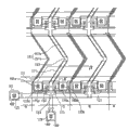
Fig. 1 is the layout of LCD according to an embodiment of the invention, and Fig. 2 is the cut-open view of LCD shown in Figure 1 II-II ' along the line intercepting.
As shown in Figure 2, LCD comprises tft array plate 100, common electrical pole plate 200 and places between plate 100 and 200 and comprise the LC layer 300 of a plurality of LC molecules 310 of aligning in vertical direction with respect to the surface of plate 100 and 200 according to an embodiment of the invention.
Referring to Fig. 1 and 2, many gate lines 121 and many storage electrode lines 131 are formed on the insulated substrate 110.Gate line 121 separates each other, and roughly extends in the horizontal.Gate line 121 transmission signals, and a plurality of outshots of every gate line 121 form a plurality of gate electrodes 123.
Every storage electrode line 131 roughly extends in the horizontal, and comprises the many a plurality of outshots to storage electrode 133a and 133b of formation.Storage electrode 133a and 133b have rectangle (or rhombus) shape, and are positioned near the gate electrode 123.Storage electrode line 131 is provided with predetermined voltage, such as the common electric voltage on the public electrode 270 that is applied to LCD common electrical pole plate 200.
Gate line 121 and storage electrode line 131 can have sandwich construction, and this sandwich construction comprises lower film (not shown) and the two-layer film with different physical properties of upper membrane (not shown).Upper membrane is preferably made by the metal with low-resistivity, for example such as Al or Al alloy contain aluminium (Al) metal, be used for reducing the signal delay or the voltage drop of gate line 121 and storage electrode line 131.Preferably by making such as the material of chromium (Cr), molybdenum (Mo) or Mo alloy, this material has the excellent contact performance for other material such as tin indium oxide (ITO) or indium zinc oxide (IZO) to lower film.The preferred compositions of lower film material and upper membrane material is respectively Cr and aluminium-neodymium (Al-Nd) alloy.
Gate line 121 and storage electrode line 131 laterally inclined, and this side with respect to the inclination angle on substrate 110 surfaces at about 30 degree to the scopes of about 80 degree.
Preferably by silicon nitride (SiN x) gate insulator 140 that forms is formed on gate line 121 and the storage electrode line 131.
Preferably a plurality of semiconductor islands 150 that formed by amorphous silicon hydride (a-Si) or polysilicon (p-Si) are formed on the gate insulator 140.Each semiconductor island 150 is positioned at the opposite of gate electrode 123.
Preferably be formed on the semiconductor island 150 by silicide or a plurality of Ohmic contact island 163,165a and 165b that n type impurity severe doped n+hydrogenation a-Si makes.
Semiconductor island 150 and Ohmic contact 163,165a and 165b's is laterally inclined, and its inclination angle with respect to substrate 110 is preferably spent to the scope between about 80 degree about 30.
As shown in Figure 1, many data lines 171 that are used to transmit data voltage roughly extend in a longitudinal direction and intersect with gate line 121 and storage electrode line 131.Every data line 171 alternating bendings, and comprise many to sloping portion and a plurality of longitudinal component.Pair of angled partly is connected to each other and forms the V font, and this opposite end to sloping portion is connected to each longitudinal component.The sloping portion of data line 171 and gate line 121 form about miter angle, and longitudinal component is crossed over gate electrode 123.The length of pair of angled part is about 1 to about 9 times of length of a longitudinal component, promptly accounts for this sloping portion is added about 50% to about 90% of this longitudinal component total length.
As shown in Figure 2, this many data lines 171 and many drain electrode 175a and 175b are separated from each other, and be formed on Ohmic contact 163,165a and 165b and the gate insulator 140.
This opposes about the longitudinal component of data line 171 each other to drain electrode 175a and 175b.Each longitudinal component of data line 171 comprises a plurality of outshots, makes the longitudinal component that comprises outshot form the source electrode 173 of part around drain electrode 175a and 175b.Source electrode 173 is formed on the Ohmic contact 163. Drain electrode 175a and 175b are respectively formed on Ohmic contact 165a and the 165b.
The only underlaid semiconductor of Ohmic contact 163,165a and 165b lead 150 and top data line 171 and top source electrode and drain electrode 173,175a and 175b between, and reduce contact resistance between following and top constituent element.Each drain electrode 175a or 175b comprise the enlarged that overlaps with storage electrode 133a or 133b.
Every group of gate electrode 123, source electrode 173, a pair of drain electrode 175a and 175b and semiconductor island 150 have formed a pair of TFT.This comprises TFT and is formed on the raceway groove that lays respectively in the semiconductor island 150 between source electrode 173 and drain electrode 175a and the 175b.
Similar to gate line 121 with storage electrode line 131, data line 171 and drain electrode 175a and 175b also can comprise preferably the lower film (not shown) made by Mo, Mo alloy or Cr and position thereon preferably by containing the metal upper membrane (not shown) of Al.In addition, data line 171 and drain electrode 175a and 175b also have inclined side, and it has the inclination angle scope from about 30 degree to about 80 degree.
Passivation layer 180 is formed on the expose portion that data line 171, drain electrode 175a and 175b and semiconductor island 150 do not cover by data line 171 and drain electrode 175a and 175b.Passivation layer 180 is preferably made by smooth photosensitive organic material with by the low dielectric insulation material such as a-Si:C:O and a-Si:O:F that plasma enhanced chemical vapor deposition (PECVD) forms, perhaps by making such as the inorganic material of silicon nitride and monox.Passivation layer 180 can have the double-decker that comprises bottom inoranic membrane and top organic membrane.
Passivation layer 180 has a plurality of contact hole 185a, the 185b and 189 of the end 179 of exposing drain electrode 175a and 175b and data line 171 respectively.Passivation layer 180 and gate insulator 140 have a plurality of contact holes 182 of the end 125 of exposing gate line 121.Contact hole 182,185a, 185b and 189 can have different shape, for example polygon or circle.Each contact hole 182 or 189 area are preferably greater than or equal 0.5mm * 15 μ m, and are not more than 2mm * 60 μ m.Contact hole 182,185a, 185b and 189 sidewall perhaps have stair-step appearance with the angle tilts of about 30 degree to about 85 degree.
Many pixel electrode 191a and 191b and a plurality of assisted parts (contact assistant) 192 and 199 that contact of preferably being made by ITO, IZO or Cr are formed on the passivation layer 180.
Each pixel electrode 191a or 191b are located substantially on by in data line 171, gate line 121 and storage electrode line 131 region surrounded, and form the V font.A pair of pixel electrode 191a and 191b are connected to each other by connecting portion 193, and form a pair of sub-pixel area (subpixel area) Pa and Pb.
Pixel electrode 191a and 191b by contact hole 185a and 185b and drain electrode 175a and 175b physics with electrically be connected, make pixel electrode 191a and 191b receive data voltage from drain electrode 175a and 175b.The pixel electrode 191a and the 191b that are provided with data voltage cooperate the generation electric field with public electrode 270, this electric field makes the liquid crystal molecule reorientation that is provided with therebetween.
Pixel electrode 191a or 191b and public electrode form the capacitor that is called " liquid crystal capacitor ", the voltage that this capacitor is applied by the back storage at TFT.The building-out condenser of the what is called " holding capacitor " in parallel with this liquid crystal capacitor is set, to improve the store voltages capacity.Holding capacitor is realized by pixel electrode 191 is overlapped with storage electrode line 131.By the outshot that forms storage electrode 133a and 133b is set at storage electrode line 131 places, prolong the drain electrode 175a and the 175b that are connected with 191b with pixel electrode 191a, and in the storage electrode 133a of drain electrode 175a and setting of 175b place and storage electrode line 131 and the enlarged that 133b overlaps, the electric capacity of holding capacitor (being memory capacitance) is increased.These design factors have reduced the distance between terminal, and have increased the overlapping area, cause the increase of memory capacitance.Pixel electrode 191a and 191b can also overlap to increase aperture opening ratio with data line 171.
Contact assisted parts 192 is connected with the exposed end 125 of gate line 121 and the exposed end 179 of data line 171 respectively with 189 by contact hole 182 with 199.Contact assisted parts 192 and 199 not necessarily, and is but preferred, with protection expose portion 125 and 179 and replenish expose portions 125 and 179 and the adhesion of external devices.
Both alignment layers (alignment layer) 11 is formed on pixel electrode 191a and 191b, contact assisted parts 192 and 199 and passivation layer 180 on.
For common electrical pole plate 200, be used to prevent the insulated substrate 210 that black matrix (black matrix) 220 that light leaks is formed on such as clear glass.Black matrix 220 comprises pixel-oriented electrode 191a and 191b and has basically and pixel electrode 191a and the identical shaped a plurality of openings of 191b.
A plurality of red, green and blue color filters 230 are formed in the opening of black matrix 220 with its major part, and overlayer (overcoat) 250 is formed on the color filter 230.
Preferably be formed on the overlayer 250 by the public electrode of making such as the transparent conductive material of ITO and IZO 270.Public electrode 270 has a plurality of otch 271 and 272.Gap alignment between each otch 271 and a pair of pixel electrode 191a and the 191b, and have two the main limits parallel to two pairs of stiles of pixel electrode 191a and 191b with this.As shown in the figure, otch 271 can overlap with the limit of pixel electrode 191a and 191b.Otch 271 is set controls the vergence direction of LC molecule in the LC layer 300, and preferably have about 9 microns width to about 12 micrometer ranges.The end of otch 271 can have different shape.Otch 272 is aimed at data line 171, and is set to be used for to reduce the delay of the data voltage that data line 171 flows.This delay is because of producing by the formed stray capacitance of overlapping of public electrode 270 with data line 171.Otch 272 also is used to control the vergence direction of the LC molecule of LC layer 300.
The both alignment layers 12 of homogeneity (homogeneous) or homotype (homeotropic) covers on the public electrode 270.
A pair of polaroid (not shown) is arranged on the outside surface of plate 100 and 200, makes their light transmission shaft (transmissive axis) intersect, and in the light transmission shaft one is parallel to gate line 121.
This LCD can also comprise the sluggish film (for example producing the optical element of all-wave, half-wave or quarter-wave phase change such as polarized light) of one deck at least of the sluggishness that is used to compensate LC layer 300.
LC molecule in the LC layer 300 is aligned, and makes their major axis perpendicular to the surface of plate 100 and 200.Liquid crystal layer 300 has negative dielectric anisotropy.
Applying common electric voltage to public electrode 270 and apply data voltage to pixel electrode 191a and 191b the time, produce the main electric field on the surface that is substantially perpendicular to plate 100 and 200.This electric field of LC molecules in response and be tending towards changing their orientation makes their major axis perpendicular to this direction of an electric field.
This main electric field has been upset on the otch 271 of public electrode 270 and the limit of pixel electrode 191a and 191b, makes it to have the horizontal component of the vergence direction of definite LC molecule.The horizontal component of main electric field has adopted four different orientations, thereby has formed four farmlands with Different L C molecule tilt direction in LC layer 300.This horizontal component is perpendicular to first and second limits of otch 271, perpendicular to the limit of pixel electrode 191a, and perpendicular to the limit of pixel electrode 191b.Therefore, four farmlands with different vergence directions form in LC layer 300.Otch 271 can replace with a plurality of projectioies that are formed on the public electrode 270, because the vergence direction of LC molecule also can be by a plurality of protruding (not shown) controls.
Because the direction of the inferior electric field that the voltage difference between pixel electrode 191a and the 191b causes is perpendicular to each limit of otch 271.Therefore, the direction of an electric field of inferior electric field is consistent with the horizontal component of main electric field.Therefore, the inferior electric field between pixel electrode 191a and the 191b has improved the vergence direction of LC molecule.
Because LCD reverses (polarity reversal that is about to the voltage that applied), such as a counter-rotating, row counter-rotating or the like, provide the data voltage that has with the common electric voltage opposite polarity to obtain by pixel electrode to vicinity so improve the inferior electric field of the vergence direction of LC molecule.The direction of the inferior electric field that produces between the adjacent pixel electrodes as a result, is equal to the horizontal component of the main electric field that produces between public electrode and the pixel electrode.So the inferior electric field between the adjacent pixel electrodes can produce, thereby improve the stability on farmland.
The vergence direction on all farmlands has formed the angles of about 45 degree with respect to gate line 121, and gate line 121 is parallel to or perpendicular to the limit of plate 100 and 200.Because 45 degree of the light transmission shaft of vergence direction and polaroid intersect the transmissivity that causes maximum, make the light transmission shaft of polaroid be parallel to or perpendicular to the limit of plate 100 and 200 so can join attached polaroid, thus the reduction manufacturing cost.
Referring to Fig. 1 and 2, this is positioned between data line 171 and pixel electrode 191a, the 191b about the symmetry of gate electrode 123 and data line 171 respectively pixel electrode 191a and 191b TFT and this, and has formed constant stray capacitance between gate electrode 123 and drain electrode 175a, 175b.As a result, the luminance difference between exposure region reduces.
Should be noted that data line 171 can remedy by widening data line 171 because of the increase resistance that its warp architecture causes.In addition, increase again and can compensate because of data line 171 width increase the electrical field deformation and the stray capacitance that cause by the size of increase pixel electrode 191a and 191b and by adapting to thick organic passivation layer.
In the method for making the tft array plate shown in Fig. 1 and 2, many storage electrode lines 131 that comprise many gate lines 121 of a plurality of gate electrodes 123 and comprise a plurality of storage electrode 133a and 133b are formed on the insulated substrate 110 such as clear glass.
If gate line 121 and storage electrode line 131 have the double-decker that comprises lower guide electrolemma and upper guide electrolemma, then the lower guide electrolemma is preferably by making such as the material with good physical and chemical characteristic of Cr or Mo alloy, and the upper guide electrolemma is preferably by Al or contain the manufacturing of Al metal.
At sequential aggradation thickness about 1,500 to about 5,000
Figure C20041003121300141
Gate insulator 140, thickness about 500 to about 2,000
Figure C20041003121300142
Intrinsic a-Si layer and thickness about 300 to about 600
Figure C20041003121300143
Extrinsic a-Si layer after, on gate insulator 140, form a plurality of extrinsic semiconductors island and a plurality of intrinsic semiconductors island 150 thereby carry out photoetching.
Form many data lines 171 and a plurality of drain electrode 175a and the 175b that comprise a plurality of source electrodes 173 thereafter.
, remove extrinsic semiconductor island not by the part of data line 171 and drain electrode 175a and 175b covering, thereby finish a plurality of Ohmic contact island 163 and 165 thereafter, and expose portion intrinsic semiconductor island 150.Preferably carry out oxygen plasma treatment, with the exposed surface on stabilization of semiconductor island 150 thereafter.
Passivation layer 180 is formed by the photosensitive organic insulating material such as the propenyl material, and is deposited on the current structure.After deposit passivation layer 180, composition passivation layer 180 and gate insulator 140 expose a plurality of contact holes 182,185a, the 185b and 189 of gate line 121 ends 125, drain electrode 175a and 175b and data line 171 ends 179 respectively thereby form.
At last, by sputter and photoetching thickness about 400 to about 500
Figure C20041003121300151
IZO or ITO layer, on passivation layer 180, form a plurality of pixel electrode 191a and 191b and a plurality of assisted parts 192 and 199 of contacting.
Fig. 3 is the layout of LCD according to another embodiment of the present invention, and Fig. 4 is the cut-open view of LCD shown in Figure 3 IV-IV ' along the line intercepting.
Shown in Fig. 3 and 4, comprise the components identical shown in some and Fig. 1 and 2 according to the layer structure of the tft array plate of the LCD of this embodiment.In the structure shown in Fig. 3 and 4, comprise many gate lines 121 of a plurality of gate electrodes 123 and comprise that many storage electrode lines 131 of a plurality of storage electrode 133a and 133b are formed on the substrate 110.Gate insulator 140, a plurality of semiconductor bar 152 and a plurality of Ohmic contact bar and island 163 and 165 orders are formed on the substrate 110 that comprises gate line 121, gate electrode 123, storage electrode line 131 and storage electrode 133a, 133b.Comprise that many data lines 171 of a plurality of source electrodes 173 and a plurality of drain electrode 175a and 175b are formed on Ohmic contact 163 and 165, and passivation layer 180 and both alignment layers 11 orders form thereon.A plurality of contact holes 182,185a, 185b and 189 are arranged in passivation layer 180 and/or the gate insulator 140, and a plurality of pixel electrode 191a is formed on the passivation layer 180 with 191b and a plurality of assisted parts 192 and 199 that contacts.
Comprise the components identical shown in some and Fig. 1 and 2 according to the layer structure of the common electrical pole plate of LCD embodiment illustrated in fig. 4.For example, order forms black matrix 220, overlayer 250, public electrode 270 and both alignment layers 21 on insulated substrate 210.
Different with the tft array plate shown in Fig. 1 and 2, extend semiconductor bar 152 and Ohmic contact 163 according to the tft array plate of the embodiment shown in Fig. 3 and 4 along data line 171.In addition, semiconductor bar 152 has and data line 171 and drain electrode 175a and 175b and following Ohmic contact 163 and 165 essentially identical flat shapes, except the channel part of TFT.
In addition, different with the LCD of Fig. 1 and 2, below passivation layer 180, form a plurality of red, green and blue color filter R, G and B, and on upper plate 200, do not have color filter with respect to pixel electrode 191a and 191b.In addition, contact hole 185a and 185b pass color filter R, G and B.Two adjacent color filters can overlap each other among color filter R, G and the B, to promote preventing that light from leaking.
One photoetching process of manufacture method utilization of tft array plate forms data line 171, drain electrode 175a and 175b, semiconductor bar 152 and Ohmic contact 163 and 165 simultaneously according to an embodiment of the invention.The photoresist figure that is used for photoetching process has the thickness that depends on the position, and it especially has the less thickness part that is positioned on the TFT raceway groove.Therefore, can save extra photo-mask process, thus simplified manufacturing technique.
Though herein with reference to description of drawings exemplary embodiment, should be understood that the present invention is not limited to these specific embodiments, and those skilled in the art can do various variations and change to it under situation about not departing from the scope of the present invention with spirit.Variation that all are such and change are confirmed as being included in the defined scope of the present invention of claims.

Claims (30)

1. LCD comprises:
First substrate, it comprises formation a plurality of pixel electrodes thereon, each in described a plurality of pixel electrodes has first and second portion;
Second substrate, it comprises formation public electrode thereon, wherein one gap, this second substrate and this first substrate interval;
Be formed at least one otch in this public electrode, wherein the spaced-apart alignment between this at least one otch and this first and second part; And
Be used to transmit many data lines of data voltage, it is formed on this first substrate, and the described interval between described first and second parts of each of wherein said pixel electrode is aimed at one of described data line.
2. LCD as claimed in claim 1, wherein this first and this second portion are connected to each other.
3. LCD as claimed in claim 1, wherein this gap comprises the liquid crystal layer that is configured to hold liquid crystal molecule, and this at least one otch comprises second limit of the edge in the face of this second portion first limit of locating and the location, an edge of facing this first that is parallel to this second portion that are parallel to this first.
4. LCD as claimed in claim 3, the horizontal component at least a location in the following manner that is used for causing the variation of liquid crystal molecules tilt direction that wherein produces electric field between this public electrode and this pixel electrode: perpendicular to this first limit of this otch; This second limit perpendicular to this otch; This edge perpendicular to this first; And perpendicular to this edge of this second portion.
5. LCD as claimed in claim 1, wherein this at least one otch has 9 microns width to 12 micrometer ranges.
6. LCD as claimed in claim 3 wherein produces an electric field between this first and this second portion, and the direction of this electric field is at least a in the following direction: perpendicular to this first limit of this at least one otch; And perpendicular to this second limit of this at least one otch.
7. LCD as claimed in claim 1, wherein have be applied to this public electrode on the voltage of the opposite polarity of voltage be applied in this first and this second portion one, and between this first and this second portion generation one electric field.
8. LCD as claimed in claim 7, wherein this electric field causes because of the voltage difference between this first and this second portion.
9. LCD as claimed in claim 1 also comprises:
Be formed at least one gate electrode on this first substrate; And
Be formed at least one pair of transistor on this first substrate, wherein be symmetrically arranged with pair of transistor about each gate electrode, to cross over a plurality of exposure regions of this first substrate, between this at least one gate electrode and this at least one pair of transistor drain electrode, form constant stray capacitance.
10. LCD as claimed in claim 9, wherein a pair of this symmetrically arranged transistor comprise a gate electrode, a source electrode, two drain electrodes and a semiconductor island.
11. LCD as claimed in claim 1, wherein this first and second part is symmetrical arranged about this data line, to cross over a plurality of exposure regions on this first substrate, forms constant stray capacitance between this first and second part and this data line.
12. LCD as claimed in claim 1 also comprises:
Be formed on many gate lines that are used to transmit signal on this first substrate;
Be formed on many storage electrode lines that are used to transmit at least one predetermined voltage on this first substrate.
13. LCD as claimed in claim 12, wherein this first and this second portion are positioned at by these many gate lines, these many storage electrode lines and this many data line area surrounded.
14. LCD as claimed in claim 1, wherein an overlapping at least one in this first and this second portion and these many data lines.
15. LCD as claimed in claim 12, wherein many gate lines of these many data lines and this and these many storage lines intersect.
16. LCD as claimed in claim 1, wherein each the bar data line in these many data lines is crooked, and comprises many sloping portions of V font that form being connected with each other.
17. LCD as claimed in claim 16, wherein the end that deviates from mutually of this sloping portion is connected with each longitudinal component that strides across gate electrode.
18. LCD as claimed in claim 17, wherein the length of every pair of this sloping portion is 1 to 9 times of length of longitudinal component.
19. LCD as claimed in claim 12, wherein at least one in these many gate lines, these many storage electrode lines and this many data lines comprise prism, and wherein said prism is spent to the scopes of 80 degree 30 with respect to the inclination angle on this first level of base plate surface.
20. LCD as claimed in claim 12, wherein at least one in these many gate lines, these many storage electrode lines and this many data lines comprise a lower film and a upper membrane.
21. LCD as claimed in claim 20, wherein this upper membrane comprises aluminum or aluminum alloy, and this lower film comprises chromium, molybdenum or molybdenum alloy.
22. LCD as claimed in claim 1 also comprises:
Be formed on a plurality of storage electrodes on this first substrate; And
Be formed on a plurality of drain electrodes on this first substrate, wherein at least one pair of storage electrode at least one pair of drain electrode in these a plurality of drain electrodes and these a plurality of storage electrodes overlaps.
23. LCD as claimed in claim 1 also comprises:
Be formed on a plurality of drain electrodes on this first substrate, wherein this first and this second portion are connected to one first drain electrode and one second drain electrode in these a plurality of drain electrodes respectively, and this first and this second portion receive the data voltage from this first drain electrode and this second drain electrode respectively.
24. LCD as claimed in claim 1 also comprises a plurality of color filters on that is formed in this first substrate and this second substrate, wherein two adjacent color filters in these a plurality of color filters overlap each other.
25. LCD as claimed in claim 1 also comprises:
Be formed on the gate insulator on this first substrate;
Be formed on a plurality of semiconductor islands on this gate insulator;
Be formed on a plurality of Ohmic contact on the described semiconductor island; And
Be formed on a plurality of drain electrodes on the described Ohmic contact, wherein said Ohmic contact has and described data line and the roughly the same flat shape of described drain electrode.
26. LCD as claimed in claim 1 also comprises:
Be formed on the gate insulator on this first substrate;
Be formed on a plurality of semiconductor islands on this gate insulator;
Be formed on a plurality of Ohmic contact on the described semiconductor island; And
Be formed on a plurality of drain electrodes on the described Ohmic contact, wherein these many data lines be formed on this Ohmic contact and this gate insulator one of at least on, and wherein said data line, described drain electrode, described semiconductor island utilize photoetching process to form simultaneously with described Ohmic contact.
27. LCD as claimed in claim 16, wherein this pixel electrode has at least two borders on the border that is parallel to this sloping portion.
28. LCD as claimed in claim 27 also comprises:
Many gate lines, it intersects with this data line and transmits signal; And
A plurality of thin film transistor (TFT)s, it is connected respectively to this gate line, this data line and this pixel electrode.
29. LCD as claimed in claim 28, wherein this thin film transistor (TFT) has first and second thin film transistor (TFT)s that are connected respectively to this first and second part.
30. LCD as claimed in claim 1, wherein this first and the marginal portion of this second portion this data line that overlaps.
CNB2004100312137A 2003-05-20 2004-03-26 Liquid crystal display and thin film transistor array panel therefor Expired - Fee Related CN100414406C (en)

Applications Claiming Priority (3)

Application Number Priority Date Filing Date Title
KR1020030031841A KR100569718B1 (en) 2003-05-20 2003-05-20 Multi-domain liquid crystal display
KR0031841/03 2003-05-20
KR0031841/2003 2003-05-20

Related Child Applications (1)

Application Number Title Priority Date Filing Date
CN2008101448715A Division CN101329482B (en) 2003-05-20 2004-03-26 LCD and thin film transistor array plate

Publications (2)

Publication Number Publication Date
CN1573479A CN1573479A (en) 2005-02-02
CN100414406C true CN100414406C (en) 2008-08-27

Family

ID=36970435

Family Applications (2)

Application Number Title Priority Date Filing Date
CN2008101448715A Expired - Fee Related CN101329482B (en) 2003-05-20 2004-03-26 LCD and thin film transistor array plate
CNB2004100312137A Expired - Fee Related CN100414406C (en) 2003-05-20 2004-03-26 Liquid crystal display and thin film transistor array panel therefor

Family Applications Before (1)

Application Number Title Priority Date Filing Date
CN2008101448715A Expired - Fee Related CN101329482B (en) 2003-05-20 2004-03-26 LCD and thin film transistor array plate

Country Status (6)

Country Link
US (3) US7046323B2 (en)
EP (1) EP1480070B1 (en)
JP (1) JP4733363B2 (en)
KR (1) KR100569718B1 (en)
CN (2) CN101329482B (en)
TW (1) TWI341408B (en)

Families Citing this family (17)

* Cited by examiner, † Cited by third party
Publication number Priority date Publication date Assignee Title
JP4550484B2 (en) * 2003-05-13 2010-09-22 三星電子株式会社 Thin film transistor array panel and multi-domain liquid crystal display device including the same
KR101006436B1 (en) * 2003-11-18 2011-01-06 삼성전자주식회사 Thin film transistor array panel for display device
JP2005258414A (en) * 2004-02-12 2005-09-22 Seiko Instruments Inc Liquid crystal display device and its manufacturing method
TWI379113B (en) * 2004-07-07 2012-12-11 Samsung Display Co Ltd Array substrate, manufacturing method thereof and display device having the same
EP1674922A1 (en) * 2004-12-27 2006-06-28 Samsung Electronics Co., Ltd. Liquid crystal display
KR101337265B1 (en) * 2004-12-27 2013-12-05 삼성디스플레이 주식회사 Thin film transistor array panel and liquid crystal display including the same
KR20070051045A (en) * 2005-11-14 2007-05-17 삼성전자주식회사 Liquid crystal display
KR101201969B1 (en) 2005-12-23 2012-11-15 삼성디스플레이 주식회사 Liquid crystal display
US8144291B2 (en) * 2006-07-20 2012-03-27 Sharp Kabushiki Kaisha Display device and production method thereof
KR101300184B1 (en) 2006-08-03 2013-08-26 삼성디스플레이 주식회사 Liquid crystal display
US8125584B2 (en) 2007-01-17 2012-02-28 Sharp Kabushiki Kaisha Liquid crystal display panel and liquid crystal display device
KR101427708B1 (en) * 2007-02-01 2014-08-11 삼성디스플레이 주식회사 Liquid crystal display panel
JP5079448B2 (en) * 2007-10-24 2012-11-21 株式会社ジャパンディスプレイウェスト Liquid crystal device and electronic device including the same
BRPI0822402A2 (en) * 2008-04-22 2015-06-16 Sharp Kk Liquid crystal monitor device
CN102608815A (en) * 2012-03-22 2012-07-25 深圳市华星光电技术有限公司 Liquid crystal display panel and manufacturing method thereof
KR20140111874A (en) * 2013-03-12 2014-09-22 삼성디스플레이 주식회사 Liquid display device
JP2014222483A (en) * 2013-05-14 2014-11-27 株式会社ジャパンディスプレイ Electronic component

Citations (8)

* Cited by examiner, † Cited by third party
Publication number Priority date Publication date Assignee Title
US5040875A (en) * 1987-07-22 1991-08-20 Nec Corporation Active matrix liquid crystal display having a high contrast ratio
US5132819A (en) * 1990-01-17 1992-07-21 Kabushiki Kaisha Toshiba Liquid-crystal display device of active matrix type having connecting means for repairing defective pixels
US5343216A (en) * 1989-01-31 1994-08-30 Sharp Kabushiki Kaisha Active matrix substrate and active matrix display apparatus
US6278503B1 (en) * 1999-01-20 2001-08-21 Sanyo Electric Co., Ltd. Vertical orientation type liquid crystal display having conductive film reducing the influence of electrical field caused by the storage capacitor line on the liquid crystal
US20020113929A1 (en) * 2001-02-19 2002-08-22 Seiko Epson Corporation Active-matrix liquid crystal display with line/column inversion drives, and electronic device therefor
US20020113931A1 (en) * 2000-11-14 2002-08-22 Seung-Beom Park Liquid crystal display having improved contrast ratio and color reproduction when viewed in the lateral direction
US6476447B1 (en) * 1992-02-05 2002-11-05 Semiconductor Energy Laboratory Co., Ltd. Active matrix display device including a transistor
CN1105328C (en) * 1998-10-13 2003-04-09 三星电子株式会社 Liquid crystal displayer with wide visual angle

Family Cites Families (28)

* Cited by examiner, † Cited by third party
Publication number Priority date Publication date Assignee Title
JP2669954B2 (en) * 1991-05-08 1997-10-29 シャープ株式会社 Active matrix display
TW476451U (en) * 1991-08-23 2002-02-11 Semiconductor Energy Lab Semiconductor device
US5193018A (en) * 1991-10-28 1993-03-09 Industrial Technology Research Institute Active matrix liquid crystal display system using complementary thin film transistors
DE69434302T2 (en) * 1993-07-27 2005-12-29 Sharp K.K. A liquid crystal display device
US5434690A (en) * 1993-07-27 1995-07-18 Kabushiki Kaisha Toshiba Liquid crystal device with pixel electrodes in an opposed striped form
JP3367176B2 (en) * 1993-11-04 2003-01-14 ジェイエスアール株式会社 Method for producing thermoplastic norbornene resin molded article
CN1105328A (en) 1994-11-09 1995-07-19 王浩 Multipurpose tricycle made by reforming bicycle
JPH10186366A (en) * 1996-12-26 1998-07-14 Fujitsu Ltd Liquid crystal display device
EP2085815B1 (en) * 1997-06-12 2013-03-13 Sharp Kabushiki Kaisha Vertically aligned (VA) liquid-crystal display device
KR19990026575A (en) 1997-09-25 1999-04-15 윤종용 Thin film transistor substrate for liquid crystal display device having pixel defect relief structure
US7301595B2 (en) * 1997-10-01 2007-11-27 Sanyo Electric Co., Ltd. Vertically aligned liquid crystal display
KR100309918B1 (en) * 1998-05-16 2001-12-17 윤종용 Liquid crystal display having wide viewing angle and method for manufacturing the same
KR100354904B1 (en) * 1998-05-19 2002-12-26 삼성전자 주식회사 Liquid crystal display with wide viewing angle
JP3427729B2 (en) * 1998-05-26 2003-07-22 松下電器産業株式会社 Liquid crystal display device, substrate for liquid crystal display device, and method of manufacturing the same
US6900869B1 (en) * 1998-11-25 2005-05-31 Lg. Philips Lcd Co., Ltd. Multi-domain liquid crystal display device with particular dielectric structures
US7119870B1 (en) 1998-11-27 2006-10-10 Sanyo Electric Co., Ltd. Liquid crystal display device having particular drain lines and orientation control window
KR100357216B1 (en) * 1999-03-09 2002-10-18 엘지.필립스 엘시디 주식회사 Multi-domain liquid crystal display device
KR100635940B1 (en) * 1999-10-29 2006-10-18 삼성전자주식회사 A vertically aligned mode liquid crystal display
KR100504532B1 (en) * 1999-12-28 2005-08-03 엘지.필립스 엘시디 주식회사 Multi-domain liquid crystal display device
KR100840308B1 (en) * 2000-06-13 2008-06-20 삼성전자주식회사 A vertically aligned liquid crystal display having the optimum domain size
TW573166B (en) * 2000-12-13 2004-01-21 Au Optronics Corp Wide viewing angle liquid crystal display
JP2002357843A (en) * 2001-06-04 2002-12-13 Matsushita Electric Ind Co Ltd Liquid crystal display panel
JP4019697B2 (en) 2001-11-15 2007-12-12 株式会社日立製作所 Liquid crystal display
EP1313220A1 (en) 2001-11-19 2003-05-21 Motorola, Inc. Apparatus for generating multiple clock signals of different frequency characteristics
KR20030042221A (en) * 2001-11-22 2003-05-28 삼성전자주식회사 a thin film transistor array panel for a liquid crystal display
KR100848087B1 (en) 2001-12-11 2008-07-24 삼성전자주식회사 Method for forming pattern on substrate and method for fabricating liquid crystal display using the same
US6922183B2 (en) * 2002-11-01 2005-07-26 Chin-Lung Ting Multi-domain vertical alignment liquid crystal display and driving method thereof
KR100929675B1 (en) 2003-03-24 2009-12-03 삼성전자주식회사 Multi-domain liquid crystal display device and thin film transistor substrate thereof

Patent Citations (8)

* Cited by examiner, † Cited by third party
Publication number Priority date Publication date Assignee Title
US5040875A (en) * 1987-07-22 1991-08-20 Nec Corporation Active matrix liquid crystal display having a high contrast ratio
US5343216A (en) * 1989-01-31 1994-08-30 Sharp Kabushiki Kaisha Active matrix substrate and active matrix display apparatus
US5132819A (en) * 1990-01-17 1992-07-21 Kabushiki Kaisha Toshiba Liquid-crystal display device of active matrix type having connecting means for repairing defective pixels
US6476447B1 (en) * 1992-02-05 2002-11-05 Semiconductor Energy Laboratory Co., Ltd. Active matrix display device including a transistor
CN1105328C (en) * 1998-10-13 2003-04-09 三星电子株式会社 Liquid crystal displayer with wide visual angle
US6278503B1 (en) * 1999-01-20 2001-08-21 Sanyo Electric Co., Ltd. Vertical orientation type liquid crystal display having conductive film reducing the influence of electrical field caused by the storage capacitor line on the liquid crystal
US20020113931A1 (en) * 2000-11-14 2002-08-22 Seung-Beom Park Liquid crystal display having improved contrast ratio and color reproduction when viewed in the lateral direction
US20020113929A1 (en) * 2001-02-19 2002-08-22 Seiko Epson Corporation Active-matrix liquid crystal display with line/column inversion drives, and electronic device therefor

Also Published As

Publication number Publication date
JP2004348131A (en) 2004-12-09
CN101329482B (en) 2011-11-16
TWI341408B (en) 2011-05-01
JP4733363B2 (en) 2011-07-27
US20040233367A1 (en) 2004-11-25
EP1480070A2 (en) 2004-11-24
CN101329482A (en) 2008-12-24
US7046323B2 (en) 2006-05-16
KR100569718B1 (en) 2006-04-10
EP1480070A3 (en) 2005-08-17
CN1573479A (en) 2005-02-02
US20060203173A1 (en) 2006-09-14
US20110109825A1 (en) 2011-05-12
KR20040099749A (en) 2004-12-02
EP1480070B1 (en) 2017-06-07
US8334958B2 (en) 2012-12-18
TW200502631A (en) 2005-01-16
US7872700B2 (en) 2011-01-18

Similar Documents

Publication Publication Date Title
CN100507687C (en) Liquid crystal display and panel therefor
CN100414406C (en) Liquid crystal display and thin film transistor array panel therefor
CN1808252B (en) Thin film transistor array panel and liquid crystal display including the panel
CN1908789B (en) Liquid crystal display device
US7292303B2 (en) Liquid crystal display and panel therefor including regular and successive regular domain defining members
US20100060838A1 (en) Liquid crystal display and method thereof
US20070182908A1 (en) Liquid crystal display and thin film transistor array panel therefor
TWI390317B (en) Liquid crystal display and thin film transistor array panel thereof
US20040233343A1 (en) Liquid crystal display and thin film transistor array panel therefor
US7773165B2 (en) Liquid crystal display
CN100517727C (en) Thin film transistor array panel
KR20090027474A (en) Liquid crystal display
US7474363B2 (en) Liquid crystal display and panel therefor
US20050018111A1 (en) Liquid crystal display and manufacturing method thereof
US7847889B2 (en) Panel for display device with light blocking on blue color filter and liquid crystal display
US7242451B2 (en) Thin film transistor array panel
US5663575A (en) Liquid crystal display device providing a high aperture ratio
US20060023151A1 (en) Liquid crystal display and panel therefor
US7755734B2 (en) Liquid crystal display and thin film transistor array panel therefor
US20090066900A1 (en) Liquid crystal display
US20060092116A1 (en) Liquid crystal display
CN101290939A (en) Liquid crystal display and it thin film transistor array substrate

Legal Events

Date Code Title Description
C06 Publication
PB01 Publication
C10 Entry into substantive examination
SE01 Entry into force of request for substantive examination
C14 Grant of patent or utility model
GR01 Patent grant
ASS Succession or assignment of patent right

Owner name: SAMSUNG DISPLAY CO., LTD.

Free format text: FORMER OWNER: SAMSUNG ELECTRONICS CO., LTD.

Effective date: 20121101

C41 Transfer of patent application or patent right or utility model
TR01 Transfer of patent right

Effective date of registration: 20121101

Address after: Gyeonggi Do, South Korea

Patentee after: Samsung Display Co., Ltd.

Address before: Gyeonggi Do, South Korea

Patentee before: Samsung Electronics Co., Ltd.

CF01 Termination of patent right due to non-payment of annual fee

Granted publication date: 20080827

Termination date: 20160326

CF01 Termination of patent right due to non-payment of annual fee