CN100423221C - Method for manufacturing electrical contact element for testing electro device and electrical contact element thereby - Google Patents
Method for manufacturing electrical contact element for testing electro device and electrical contact element thereby Download PDFInfo
- Publication number
- CN100423221C CN100423221C CNB028277597A CN02827759A CN100423221C CN 100423221 C CN100423221 C CN 100423221C CN B028277597 A CNB028277597 A CN B028277597A CN 02827759 A CN02827759 A CN 02827759A CN 100423221 C CN100423221 C CN 100423221C
- Authority
- CN
- China
- Prior art keywords
- groove
- electric contacts
- tip portion
- header portion
- sacrificial substrate
- Prior art date
- Legal status (The legal status is an assumption and is not a legal conclusion. Google has not performed a legal analysis and makes no representation as to the accuracy of the status listed.)
- Expired - Fee Related
Links
Images


Classifications
-
- G—PHYSICS
- G01—MEASURING; TESTING
- G01R—MEASURING ELECTRIC VARIABLES; MEASURING MAGNETIC VARIABLES
- G01R3/00—Apparatus or processes specially adapted for the manufacture or maintenance of measuring instruments, e.g. of probe tips
-
- G—PHYSICS
- G01—MEASURING; TESTING
- G01R—MEASURING ELECTRIC VARIABLES; MEASURING MAGNETIC VARIABLES
- G01R1/00—Details of instruments or arrangements of the types included in groups G01R5/00 - G01R13/00 and G01R31/00
- G01R1/02—General constructional details
- G01R1/06—Measuring leads; Measuring probes
- G01R1/067—Measuring probes
- G01R1/06711—Probe needles; Cantilever beams; "Bump" contacts; Replaceable probe pins
- G01R1/06716—Elastic
- G01R1/06727—Cantilever beams
-
- G—PHYSICS
- G01—MEASURING; TESTING
- G01R—MEASURING ELECTRIC VARIABLES; MEASURING MAGNETIC VARIABLES
- G01R1/00—Details of instruments or arrangements of the types included in groups G01R5/00 - G01R13/00 and G01R31/00
- G01R1/02—General constructional details
- G01R1/06—Measuring leads; Measuring probes
- G01R1/067—Measuring probes
- G01R1/06711—Probe needles; Cantilever beams; "Bump" contacts; Replaceable probe pins
- G01R1/06733—Geometry aspects
-
- G—PHYSICS
- G01—MEASURING; TESTING
- G01R—MEASURING ELECTRIC VARIABLES; MEASURING MAGNETIC VARIABLES
- G01R1/00—Details of instruments or arrangements of the types included in groups G01R5/00 - G01R13/00 and G01R31/00
- G01R1/02—General constructional details
- G01R1/06—Measuring leads; Measuring probes
- G01R1/067—Measuring probes
- G01R1/073—Multiple probes
- G01R1/07307—Multiple probes with individual probe elements, e.g. needles, cantilever beams or bump contacts, fixed in relation to each other, e.g. bed of nails fixture or probe card
- G01R1/07342—Multiple probes with individual probe elements, e.g. needles, cantilever beams or bump contacts, fixed in relation to each other, e.g. bed of nails fixture or probe card the body of the probe being at an angle other than perpendicular to test object, e.g. probe card
-
- H—ELECTRICITY
- H05—ELECTRIC TECHNIQUES NOT OTHERWISE PROVIDED FOR
- H05K—PRINTED CIRCUITS; CASINGS OR CONSTRUCTIONAL DETAILS OF ELECTRIC APPARATUS; MANUFACTURE OF ASSEMBLAGES OF ELECTRICAL COMPONENTS
- H05K3/00—Apparatus or processes for manufacturing printed circuits
- H05K3/40—Forming printed elements for providing electric connections to or between printed circuits
- H05K3/4092—Integral conductive tabs, i.e. conductive parts partly detached from the substrate
Landscapes
- Physics & Mathematics (AREA)
- General Physics & Mathematics (AREA)
- Geometry (AREA)
- Measuring Leads Or Probes (AREA)
- Testing Or Measuring Of Semiconductors Or The Like (AREA)
Abstract
Disclosed is a method for manufacturing an electrical contact element used to test an electronic device, and an electrical contact element manufactured with forming the electrical contact element having the tip portion and the beam portion. The method comprises the step of conducting one or more times, after defining the trench, anisotropic etching in the trench in such a way as to increase a depth of the trench and round an inner surface of the trench. The electrical contact element comprises a beam portion having a multi-stepped configuration which comprises a three, bar-shaped part with having a width greater than the upper part. Each parts are connected at the other end thereof with an electronic component, through a bump; and a tip portion formed integrally with a free end of the first part of the beam portion.
Description
Technical field
The present invention relates to be used for the manufacture method of electric contacts of testing electronic devices and the electric contacts of making by this method, more specifically, the present invention relates to make a kind of method of electric contacts, described electric contacts can be tested this electronic installation by contacting with electronic installation, to determine whether this electronic installation is in normal condition, the invention still further relates to the electric contacts of making by this method.
In addition, the present invention relates to a kind of manufacture method of electric contacts, this electric contacts is owing to existing armrest (armrest) to increase physical force, and can the electrical testing electronic installation, the invention still further relates to the electric contacts of being made by this method.
Background technology
In general, obtain semiconductor chip by carrying out a series of semiconductor fabrications on Semiconductor substrate, described semiconductor fabrication comprises oxidizing process, diffusion process, ion implantation process, etching process, metallization processes etc.The chip for preparing on Semiconductor substrate is divided into certified products and substandard products by electric attenuation classification (EDS) test.Have only certified products to be placed in section and the encapsulation process then.
At this moment, in the EDS test, the electric contacts such as probe card is contacted with a pedestal of semiconductor chip, come it is applied the signal of telecommunication, by detecting electric response, can determine whether this chip is in normal condition then the signal of telecommunication that is applied.
Simultaneously, in by the panel display apparatus such as LCD that carry out a series of panel display apparatus manufacture processes manufacturings, electric contacts is partly contacted with the preliminary election of panel display apparatus, come it is applied the signal of telecommunication, by detecting electric response, determine whether this LCD plate is in normal condition then to the signal of telecommunication that is applied.
At present, made great efforts to research and develop, to guarantee to be used for the measuring semiconductor chip or to meet nearest development trend such as the conventional electric contacts of the normality of flat-panel monitor of LCD etc., the i.e. trend that spacing diminishes in highly integrated semiconductor device such as 1G DRAM, make conventional electric contacts have rapid response speed, in high band, has enough intensity, so that can not wear and tear owing to contacting repeatedly, keep predetermined contact resistance, having excellent conductivity, and has (OD) characteristic of enough overdriving (over-drive).
Particularly, made great efforts to research and develop, with guarantee when electric contacts repeatedly when highly integrated semiconductor device contacts, the particle that produces on electric contacts is minimum, electric contacts has excellent conductivity, and the tip portion of a plurality of electric contacts can contact to satisfy the needs of overdrive scheme with semiconductor chip pad simultaneously.
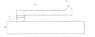
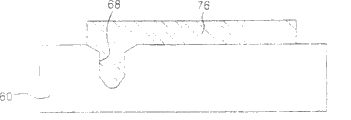
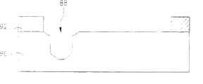
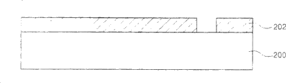
As shown in Figure 1, in the electric contacts of routine, be connected with column part 12 such as the terminal of the printed circuit board (PCB) electronic components (10) such as (PCB) that has formed predetermined circuit patterns on it.Column part 12 is connected with header portion 14, and header portion 14 is connected with tip portion 16.
At this moment, column part 12, header portion 14 and tip portion 16 provide separately and are connected by adhesive each other.Header portion 14 has the bar-shaped configuration of constant width.
Particularly, tip portion 16 has the configuration of prism shape, and it has four angles and a tip-angled shape end.
Therefore, the tip portion 16 of electric contacts contacts with semiconductor chip pad repeatedly by constant physical force F, and have the OD characteristic of hope, so that the constant signal of telecommunication is applied on the semiconductor chip, thereby confirm whether this semiconductor chip is in normal condition.
But, conventional electric contacts problem is: because tip portion has the tip-angled shape end, and the tip portion of electric contacts contacts with the pedestal (pad) of semiconductor chip repeatedly by constant physical force F, tip portion may thrust the oxidation film that forms on the pedestal and damage pedestal, and defective part must increase when carrying out the follow-up semiconductor fabrication that connects etc. such as lead-in wire thus.
In addition, because conventional electric contacts has a plurality of angles in its side, when tip portion contacted with the pedestal of semiconductor chip, the tip was worn easily and itself produces particle, and this can pollute highly integrated semiconductor chip.
Simultaneously, because the tip portion of electric contacts has angular end, the contact area between this tip portion and semiconductor chip pad can only reduce, thereby reduces conductivity.
And, when electric contacts must contact the OD characteristic of wishing with assurance by constant physical force F with semiconductor chip pad,, therefore be difficult to regulate suitably the OD characteristic because tip portion length is short.
That is to say, when multiple electric contacts is provided on the probe and arrange with the qualification predetermined profile, because the tip portion length of electric contacts is short, be difficult to suitably regulate the height of this multiple electric contacts, with the OD characteristic that obtains to wish.
Because the structure of tip portion or the development of configuration aspect also may produce the problems referred to above.
The tip portion that promptly had tungsten matter aciculiform configuration has originally developed into has V-arrangement or pyramid-shaped configuration.Prismatic tip portion has developed into and has had truncated pyramid-shaped configuration.
The shortcoming of tungsten matter aciculiform tip portion is: when pointing tip portion terminal, terminal work is manual to be carried out owing to point, and has destroyed the repeatability and the productivity ratio of tip portion.Simultaneously, because prismatic and truncated pyramid-shaped tip portion has the bight at band angle, and tip portion contacts with the pedestal of semiconductor device repeatedly, and tip portion may be worn in the bight.So, must reduce or remove the acutance in bight.
Therefore, as mentioned above, when carrying out the test of a plurality of electronic devices repeatedly, because the existence of the particle that produces in the angular end and the bight of tip portion must often be washed tip portion, the result can not in extremely rapid succession test.
In addition, when the high-frequency type electronic devices of exploitation recently obviously is subjected to noise effect, owing to tip portion is worn, thus can not be formed uniformly contact point, thus the reliability of test must be reduced.
Owing to this reason, need test at short notice, to boost productivity.
In addition, because header portion has bar-shaped configuration, so can not meet nearest development trend, the i.e. trend that spacing diminishes in highly integrated semiconductor device fully.Simultaneously, when electric contacts contacted with semiconductor chip pad by physical force F, certain some place and header portion that stress concentrates on the header portion may be destroyed.
In addition, because the join domain between header portion and tip portion is little, when electric contacts contacted with semiconductor chip pad by constant physical force F, stress focused on the join domain and tip portion may be destroyed.
In addition, when in conventional electrical device detection equipment, increasing the constant physical force that is applied on the tip portion so that when guaranteeing that OD characteristic of wishing and the oxidation film that forms may be pierced on semiconductor chip pad, owing to the various unfavorable factors that conventional electric contacts had have problems.
Specifically, in the time the length of header portion must being shortened,, be difficult to the OD characteristic that obtains to wish if shorten the length of header portion in order to increase constant physical force F, and excessive stress may be applied on the header portion part, so header portion may be destroyed.
Summary of the invention
Therefore, the present invention is devoted to solve the problem that produces in correlation technique, an object of the present invention is to provide a kind of manufacture method that is used for the electric contacts of testing electronic devices, it can overcome the problem of routine techniques, because the tip portion of conventional electric contacts has several bights on its limit, when this tip portion contacted with the pedestal of semiconductor chip, tip portion was worn and itself produces particle, and the present invention also provides the electric contacts with described method preparation.
Another object of the present invention provides a kind of manufacture method of the electric contacts that is used for detection. electronics, it can overcome the problem of routine techniques, because the tip portion of conventional electric contacts has an angular tip, reduce conductivity, the present invention also provides the electric contacts with described method preparation.
Another object of the present invention provides a kind of manufacture method of the electric contacts that is used for detection. electronics, it can overcome the problem of routine techniques, because the tip portion of conventional electric contacts has an angular tip, when tip portion contacts with semiconductor chip pad repeatedly by constant physical force, the oxidation film that forms on the tip portion perforate base also damages this pedestal, the waste product ratio increases when carrying out such as follow-up semiconductor fabrications such as lead-in wire connection procedures, and the present invention also provides the electric contacts with described method preparation.
Another object of the present invention provides a kind of manufacture method of the electric contacts that is used for detection. electronics, wherein increases the length of tip portion so that the OD characteristic that realizes easily wishing, the present invention also provides the electric contacts for preparing with this method.
Another object of the present invention provides a kind of manufacture method of the electric contacts that is used for detection. electronics, it can meet nearest trend fully, promptly such as the trend of desired pitch smaller in the highly integrated electronic installations such as semiconductor chip, the present invention also provides the electric contacts with described method preparation.
Another object of the present invention provides a kind of manufacture method of the electric contacts that is used for detection. electronics, it can overcome the problem of routine techniques, when the tip portion of conventional electric contacts contacts with semiconductor chip pad repeatedly by constant physical force, stress concentrates on certain the some place on the header portion, and header portion is damaged, and the present invention also provides the electric contacts with described method preparation.
Another object of the present invention provides a kind of manufacture method of the electric contacts that is used for detection. electronics, it can overcome the problem of routine techniques, because the join domain at the header portion of conventional electric contacts and tip portion is little, when electric contacts contacts with the pedestal of semiconductor chip repeatedly by constant physical force, stress focuses on the little join domain and tip portion is damaged, and the present invention also provides the electric contacts with described method preparation.
Another object of the present invention provides a kind of manufacture method of the electric contacts that is used for detection. electronics, this electric contacts has the repeatability of improvement with respect to its header portion and tip portion, and the present invention also provides the electric contacts with described method preparation.
Another object of the present invention provides a kind of manufacture method of the electric contacts that is used for detection. electronics, it can reduce because the damage that particle that forms on the pedestal of device and cut produce, and has the tip portion that has increased contact area, thereby improve productivity ratio, the present invention also provides the electric contacts with described method preparation.
Another object of the present invention provides a kind of manufacture method of the electric contacts that is used for detection. electronics, this electric contacts can be by increasing its physical force incoming call detection. electronics owing to there is armrest, to determine whether electronic installation is in normal condition, the present invention also provides the electric contacts with this method preparation.
To achieve these goals; according to an aspect of the present invention; a kind of manufacture method that is used for the electric contacts of detection. electronics is provided; promptly on consumptive substrate, limit the groove of the part that wherein will taper off to a point; form open region that the diaphragm pattern makes this diaphragm pattern make will to form header portion therein and be connected with described groove; filled conductive material in described open region; remove sacrificial substrate and diaphragm pattern have tip portion and header portion with formation electric contacts; this method comprises following process: after limiting groove; in groove, carry out the anisotropic etching of one or many, with the degree of depth that increases groove and make grooved inner surface become slick and sly.
According to another aspect of the present invention, carrying out the one or many anisotropic etching in groove is undertaken by reactive ion etching (RIE) method to increase gash depth and to make grooved inner surface become slick and sly process.
According to another aspect of the present invention, header portion has the multi-ladder configuration, it comprises the first bar shaped part that is connected with tip portion, the second bar shaped part that is connected with first, the width of second portion is greater than first, the 3rd bar shaped part that is connected with second portion, the width of third part is greater than second portion.Scheme as an alternative, header portion has configuration in a zigzag, it comprises the first bar shaped part that is connected with tip portion, is connected with first and second part in a zigzag of crooked one or many in a zigzag, and the 3rd bar shaped part that is connected with second portion.
According to another aspect of the present invention, the end of tip portion has the prismatic or conical butt configuration of butt polygon, and has slick and sly end surface.Scheme as an alternative, the end of tip portion has the column configuration, and has slick and sly end surface, forms projection near the near-end (proximal end) of tip portion.
According to another aspect of the present invention, a kind of manufacture method that is used for the electric contacts of testing electronic devices is provided, promptly on sacrificial substrate, limit the groove of the part that will taper off to a point therein, forming the first diaphragm pattern makes the diaphragm pattern of winning make first open region that will form header portion therein, and this open region communicates with described groove, filled conductive material in first open region, remove the sacrificial substrate and the first diaphragm pattern, the electric contacts that has tip portion and header portion with formation, described method comprises following process: after limiting groove, carry out the one or many anisotropic etching with the degree of depth that increases groove and make grooved inner surface become slick and sly in groove; Filled conductive material in first open region of the predetermined thickness of being made on sacrificial substrate by first protective layer with part and the header portion of tapering off to a point, flattens the first products obtained therefrom upper surface then; Making the second diaphragm pattern make second open region that will form armrest therein through forming the second diaphragm pattern on first products obtained therefrom of flattening course, this second open region is near the groove of the part that will taper off to a point therein; Filled conductive material in second open region that is defined predetermined thickness by second protective layer on first products obtained therefrom to form described armrest, flattens the upper surface of second products obtained therefrom then; Remove the second diaphragm pattern, first diaphragm pattern and the exhaustion layer, make have tip portion, the electric contacts of header portion and armrest.
According to another aspect of the present invention, the end of tip portion has that the butt polygon is prismatic, conical butt or column-shaped configuration, and has slick and sly tip end surface, forms projection near the near-end of tip portion.
According to another aspect of the present invention, a kind of electric contacts that is used for testing electronic devices is provided, comprise: header portion with multi-ladder configuration, this header portion comprises first bar shaped part, be connected with first and width greater than the second bar shaped part of first, link to each other with second portion with at least one section and width greater than the 3rd bar shaped part of second portion, third part links to each other with an electronic component by a projection (bump) at its other end; The corresponding position of free end that described electric contacts also is included in the first of header portion is in the groove that limits on the sacrificial substrate, it forms by using the first diaphragm pattern to carry out one or many first isotropic etching as etching mask, and its generation type makes the lower surface of groove become slick and sly; Described electric contacts also comprises tip portion, its by after removing the first diaphragm pattern the coating second diaphragm pattern on the sacrificial substrate, in groove filled conductive material, leveling products obtained therefrom upper surface, remove sacrificial substrate and the second diaphragm pattern forms by wet etching.
According to another aspect of the present invention, a kind of electric contacts that is used for testing electronic devices is provided, comprise: header portion with a plurality of zigzag configurations, this header portion comprises first bar shaped part that is connected with electronic component by a projection, is connected with first and the second zigzag part of the crooked one or many of zigzag, with the 3rd bar shaped part that links to each other with second portion; The corresponding position of free end that described electric contacts also is included in the third part of header portion is in the groove that limits on the sacrificial substrate, it forms by using the first diaphragm pattern to carry out one or many first isotropic etching as etching mask, and its generation type makes the lower surface of groove become slick and sly; Described electric contacts also comprises tip portion, its by after removing the first diaphragm pattern the coating second diaphragm pattern on the sacrificial substrate, in groove filled conductive material, leveling products obtained therefrom upper surface, remove sacrificial substrate and the second diaphragm pattern forms by wet etching.
According to another aspect of the present invention, by carrying out the one or many anisotropic etching, described groove has polygon prismatic, conical butt of butt or cylindrical portion, and has the channel side surface of inclination.
According to another aspect of the present invention, the end of tip portion has column-shaped configuration, and has slick and sly end surface, forms first and second projections (projection) near the near-end of tip portion.
According to another aspect of the present invention, provide a kind of electric contacts that is used for testing electronic devices, comprising: the sacrificial substrate of using first photoresist formation in its surface with predetermined thickness; First open region by the first photoresist patterning is limited is used to make tip portion to form therein; Use the first photoresist pattern as can taper off to a point the therein groove of part of etching mask, this groove makes the tip portion slyness through anisotropic etch process, and the first photoresist pattern that forms on sacrificial substrate is removed by ashing; The zigzag header portion and the armrest of the crooked one or many of zigzag, it carries out, flattens the upper surface of products obtained therefrom to predetermined thickness and by chemical vapor deposition (CVD), physical vapor deposition (PVD) or coating method by fill the conductive material be used to form most advanced and sophisticated and header portion in second open region of being made by the second photoresist pattern on sacrificial substrate, and removes the second photoresist pattern and the 3rd photoresist pattern and form; The column part that forms on the end of electronic component is to have the projection of preliminary dimension; And jockey, being used for the column part and being connected with an end of header portion, the described end of this header portion is relative with an end that forms armrest thereon; Wherein when removing sacrificial substrate, on the zigzag upper surface partly of crossbeam, form described armrest by wet etching.
According to another aspect of the present invention, provide a kind of electric contacts that is used for detection. electronics, it comprises: the sacrificial substrate that forms with first photoresist with predetermined thickness in its surface; Make first photoresist form first open region that pattern limited, be used for tapering off to a point therein part; Be used to use first photoresist as taper off to a point the therein groove of part of mask, this groove makes described tip portion slyness through anisotropic etch process, and the first photoresist pattern that forms on sacrificial substrate is removed by ashing; The zigzag header portion and the armrest of the crooked one or many of zigzag, its by fill in second open region of on sacrificial substrate, making by the second photoresist pattern conductive material be used to form most advanced and sophisticated and header portion to predetermined thickness the upper surface by chemical vapour deposition (CVD), physical vapour deposition (PVD) or coating method, leveling products obtained therefrom also, and remove the second photoresist pattern and the 3rd photoresist pattern and form; The column part that forms on the end of electronic component is to have the projection of preliminary dimension; And jockey, being used for the column part and being connected with an end of header portion, the described end of this header portion is relative with an end that forms armrest thereon; Wherein when removing sacrificial substrate, on the zigzag part of zigzag header portion and forming armrest respectively on the electronical elements surface, make the distance that these armrest spaces are predetermined by wet etching.
According to another aspect of the present invention, partly form under the situation of header portion in the zigzag with the crooked one or many of zigzag, described armrest forms between desired location on the zigzag part and the relevant position on the electronical elements surface.
According to another aspect of the present invention, on the header portion relative, form described armrest with tip portion.
According to another aspect of the present invention, on the zigzag of header portion part a bit and form described armrest, the most close more described tip portion between the relevant position on the electronical elements surface.
Description of drawings
After describing in detail below reading in conjunction with the accompanying drawings, above-mentioned purpose of the present invention and other features and advantage will become clearer, wherein:
Fig. 1 a and 1b are that explanation is used for the sectional view and the perspective view of conventional electric contacts of detection. electronics;
Fig. 2-10b explains that the first embodiment manufacturing according to the present invention is used for the sectional view of method of the electric contacts of detection. electronics;
Figure 11 a is the plane graph of explanation according to the header portion of the electric contacts that is used for detection. electronics of the present invention;
Figure 11 b is the plane graph of explanation according to the another kind of header portion of the electric contacts that is used for detection. electronics of the present invention;
Figure 12-18b explains that the second embodiment manufacturing according to the present invention is used for the sectional view of method of electric contacts of detection. electronics;
Figure 19-25b explains that the 3rd embodiment manufacturing according to the present invention is used for the sectional view of method of electric contacts of detection. electronics;
Figure 26 be explanation according to first embodiment of the present invention, be used for the perspective view of first electric contacts that the method for electric contacts of detection. electronics makes by manufacturing;
Figure 27 be explanation according to first embodiment of the present invention, be used for the perspective view of second electric contacts that the method for electric contacts of detection. electronics makes by manufacturing;
Figure 28 be explanation according to first embodiment of the present invention, be used for the perspective view of the 3rd electric contacts that the method for electric contacts of detection. electronics makes by manufacturing;
Figure 29 be explanation according to first embodiment of the present invention, be used for the perspective view of the 4th kind of electric contacts that the method for electric contacts of detection. electronics makes by manufacturing;
Figure 30 be explanation according to second embodiment of the present invention, be used for the perspective view of the 5th kind of electric contacts that the method for electric contacts of detection. electronics makes by manufacturing;
Figure 31 be explanation according to second embodiment of the present invention, be used for the perspective view of the 6th kind of electric contacts that the method for electric contacts of detection. electronics makes by manufacturing;
Figure 32 be explanation according to second embodiment of the present invention, be used for the perspective view of the 7th kind of electric contacts that the method for electric contacts of detection. electronics makes by manufacturing;
Figure 33 be explanation according to second embodiment of the present invention, be used for the perspective view of the 8th kind of electric contacts that the method for electric contacts of detection. electronics makes by manufacturing;
Figure 34 is the plane graph that illustrates according to a kind of layout of the electric contacts that is used for detection. electronics of the present invention;
Figure 35 illustrates the plane graph of arranging according to the another kind of the electric contacts that is used for detection. electronics of the present invention;
Figure 36 is that expression is applied to and is used for the figure of stress distribution of bar shaped header portion of conventional electric contacts of detection. electronics;
Figure 37 is that expression is applied to the figure according to the stress distribution of the zigzag header portion of the electric contacts that is used for detection. electronics of the present invention;
Figure 38 a and 38b are explanations according to the sectional view and the perspective view of electric contacts that is used for detection. electronics of the 4th embodiment of the present invention;
Figure 39 a and 39b are explanations according to the sectional view and the perspective view of electric contacts that is used for detection. electronics of the 5th embodiment of the present invention;
Figure 40 a and 40b are explanations according to the sectional view and the perspective view of electric contacts that is used for detection. electronics of the 6th embodiment of the present invention;
Figure 41 a-41f is the cross-sectional view of the header portion of the electric contacts shown in the key diagram 38a-40b;
Figure 42 a-42i explains the sectional view of method of electric contacts that is used for detection. electronics shown in shop drawings 38a and the 38b;
Figure 43 a-43d explains the sectional view of method of electric contacts that is used for detection. electronics shown in shop drawings 39a and the 39b;
Figure 44 a-44d explains the sectional view of method of electric contacts that is used for detection. electronics shown in shop drawings 40a and the 40b;
To be expression be applied to figure according to the structure that stress distribution obtained on the header portion of the electric contacts that is used for detection. electronics of the present invention by simulation to Figure 45 a;
To be expression by simulation be applied to Figure 45 b is used for the figure of the structure that stress distribution obtained on the header portion of conventional electric contacts of detection. electronics.
Specific embodiments
Present more detailed description the preferred embodiments of the invention, an one example illustrates in the accompanying drawings.Under possible situation, the identical Reference numeral of use is represented identical or similar part in all figure and specification.
Fig. 2-10b explains that the first embodiment manufacturing according to the present invention is used for the sectional view of method of electric contacts of testing electronic devices.
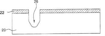
In method, as shown in Figure 2, for example forming first diaphragm 22 on the whole surface of the sacrificial substrate 20 of the silicon manufacturing of (100) with predetermined thickness with having fixed orientation according to this embodiment of the present invention.Ground floor diaphragm 22 comprises such as the film of photoresist and oxidation film.At this moment, form described photoresist by spin-coating method, in spin-coating method, photoresist is poured on the sacrificial substrate 20, rotate sacrificial substrate 20 simultaneously, oxidation film forms by conventional thermal oxidation method.
Then, as shown in Figure 3,, form the first diaphragm pattern 24 with first open region (unmarked) by the photoetching process that carries out knowing in this area.
At this moment, by having realized on it silk screen (reticle) of circuit pattern forming the first diaphragm pattern 24 that comprises photoresist applying photoresist, exposure and development on first diaphragm 22.In addition, by on first diaphragm 22, apply photoresist, by the exposure and the development products obtained therefrom prepares the photoresist pattern, use this photoresist pattern to carry out wet method as etching mask or dry etching forms the first diaphragm pattern 24 that comprises oxidation film.
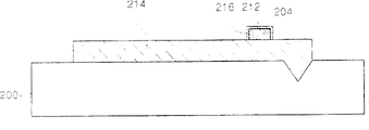
Then, shown in Fig. 4 a, carry out first etching process as etching mask, on sacrificial substrate 20, form the groove of the part that will taper off to a point therein by using the first diaphragm pattern 24.
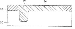
At this moment, first etching process comprises the wet etch process of using chemicals, in described chemicals, mixes potassium hydroxide (KOH) and deionized water with predetermined ratio.When adopting chemicals to carry out wet etching, sacrificial substrate 20 anisotropic etchings that will have fixed orientation, the groove 26 that has the prismatic or conical butt configuration of butt polygon with formation.
In addition, shown in Fig. 4 b, first etching process can comprise the wet etch process that adopts chemicals, in this chemicals, and hydrofluoric acid (HF), nitric acid (HNO
3) and acetic acid (CH
3COOH) mix with predetermined ratio.Wet etch process by adopting chemicals to carry out will have sacrificial substrate 20 isotropic etchings such as the fixed orientation of (100), have for example groove 28 of square column configuration and bottom surface slyness of cylindricality with formation.
At this moment, because the isotropic etching characteristic of chemicals, sacrificial substrate is in the upper end of first open region and also etched under the first diaphragm pattern 24.
Then, shown in Fig. 5 a, the first diaphragm pattern 24 that applies on sacrificial substrate 20 is as etching mask, and it limits by the laterally inclined butt polygon groove 26 prismatic or the conical butt configuration that has that first anisotropic etch process forms.In this state, adopt SF
6, C
4F
8And O
2The admixture of gas that gas mixes with predetermined ratio is implemented second etching process.
At this moment, second etching process is a kind of deep trouth etching, implements by the reactive ion etching (RIE) of so-called Bosh method.By carrying out second etching process, the degree of depth that is formed by first etching process and have the groove 26 of the prismatic or conical butt configuration of butt polygon increases to 30 μ m~500 μ m, and the bottom surface of groove 26 becomes slick and sly simultaneously.
Describe in further detail, passing through SF
6The further etched trench 26 of isotropic etching characteristic have the degree of depth of 30 μ m~500 μ m after, the angle of inner surface with groove 26 of the polygon prismatic or conical butt configuration of butt is reduced to predetermined degree, and the lower surface of groove 26 becomes slick and sly.
Here, it should be noted that second etching process can carry out one or many.
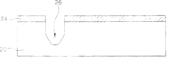
Simultaneously, shown in Fig. 5 b, use the first diaphragm pattern 24 that is applied on the sacrificial substrate 20 as etching mask, this pattern limits with the groove 28 of the column-shaped configuration with slick and sly inner surface that first etching process forms.In this state, adopt SF
6, C
4F
8And O
2The admixture of gas that gas mixes with predetermined ratio carries out second etching process.
At this moment, second etching process is a kind of deep trouth etching, and the RIE by so-called Bosh method carries out.By carrying out second etching process, the determined gash depth of first etching process increases to 30 μ m~500 μ m.Therefore, groove 28 is able to further intensification, and it is slick and sly that its basal surface becomes.
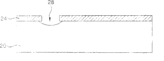
Here, it should be noted that second etching process can carry out one or many.Then; shown in Fig. 6 a; remove after the first diaphragm pattern 24; form the second diaphragm pattern 30 by second etching process on the whole surface with sacrificial substrate 20 that the polygon groove 26 prismatic or conical butt configuration and bottom surface slyness of butt limited, this pattern comprises the photoresist with predetermined thickness and limits second open region (unnumbered).Scheme as an alternative; shown in Fig. 6 b; remove after the first diaphragm pattern 24; form the second diaphragm pattern 31 by second etching process on the whole surface of the sacrificial substrate 20 that the groove 28 with column-shaped configuration and bottom surface slyness is limited, this pattern comprises the photoresist with predetermined thickness and limits second open region (unnumbered).
At this moment, form the second diaphragm pattern 30 by coating photoresist, exposure and development.The second diaphragm pattern 30 and 31 formation can limit second open region on sacrificial substrate, thereby header portion is formed in second open region, and second open region is communicated with groove 26 and 28 respectively.
Subsequently, shown in Fig. 7 a, on sacrificial substrate 20, form after the second diaphragm pattern 30, conductive materials 32 is filled in second open region, in order to have preset thickness, the upper surface of leveling products obtained therefrom by carrying out CVD, PVD or coating process.Scheme as an alternative, shown in Fig. 7 b, form on the sacrificial substrate 20 of the second diaphragm pattern form by CVD, PVD or coating method have the electric conducting material 34 of predetermined thickness after, the upper surface of leveling products obtained therefrom.
At this moment, electric conducting material is made by nickel alloy etc., can will be formed into the upper surface leveling of the sacrificial substrate 20 of material by methods such as chemical machinery polishing, etch and grindings.
Then, shown in Fig. 8 a, (a) when removing through sacrificial substrate 20 upper surfaces of screed step, the part that tapers off to a point in groove 26 forms header portion 36 in second open region referring to Fig. 7 at the second diaphragm pattern 30.Scheme as an alternative, shown in Fig. 8 b, along with the second diaphragm pattern 31 (referring to Fig. 7 b) from through the removing of sacrificial substrate 20 upper surfaces of screed step, the part that tapers off to a point in groove 28 forms header portion 38 in second open region.
At this moment, by using chemicals to carry out wet etching or carrying out dry etching such as ashing, remove the second diaphragm pattern 31 (referring to Fig. 7 b).
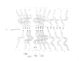
In order to meet nearest development trend fully, the i.e. trend that spacing diminishes in highly integrated semiconductor device, as shown in Figure 11 a, header portion 36 and 38 each all have the multi-ladder configuration, this configuration comprise with groove 26 and 28 in each first bar shaped part 40 that links to each other of the tip portion that forms; Link to each other with first 40 and width greater than the second bar shaped part 42 of first 40; And link to each other with second portion 42 and width greater than the 3rd bar shaped part 44 of second portion 42.
In addition, shown in Figure 11 b, crossbeam 36 and 38 each can have in a zigzag configuration, this configuration comprises the first bar shaped part 46 that links to each other with the tip portion that forms in the groove 26 and 28; Link to each other with first 46 and second part 48 in a zigzag of crooked one or many in a zigzag; And the 3rd bar shaped part 50.
At this moment, third part 40,50 can link to each other with each tip portion of formation in the groove 26,28.Equally, the angle of bend of second of the header portion 38 zigzag part 48 is 30 °~170 ° in a zigzag, preferred about 90 °.It should be noted that second portion 48 is crooked one or many in a zigzag.In each of crossbeam 36 and 38, to the tip portion position, width reduces from raised position, therefore meets nearest trend, the i.e. trend that spacing diminishes in highly integrated semiconductor device easily.
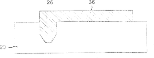
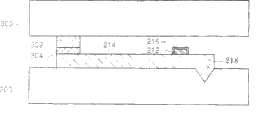
Then, shown in Fig. 9 a, linking to each other with electronic component 60, has circuit pattern on this electronic component by having the header portion 36 that forms on the sacrificial substrate 20 that the polygon groove 26 prismatic or conical butt configuration and bottom surface slyness of butt limited media by projection 62.Scheme as an alternative, shown in Fig. 9 b, the header portion 38 that forms on the sacrificial substrate 20 that is limited by the groove 28 with column-shaped configuration and bottom surface slyness links to each other with electronic component 64 by the media of projection 66, has circuit pattern on this electronic component.
At this moment, the header portion 36,38 that forms on the sacrificial substrate 20 interconnects with electronic component 60,64 respectively, after its connected mode makes that projection 62,66 places between crossbeam 36,38 and the electronic component 60,64, projection 62,66 is connected with header portion 36,38 by welding, soldering, plated film, electroconductive binder etc.
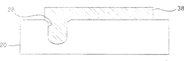
At last, shown in Figure 10 a, after the sacrificial substrate 20 that is limited by the groove 26 with polygon prism of butt or conical butt configuration and bottom surface slyness is removed by methods such as wet etchings, can make header portion 36 be able to freedom, thereby finish the electric contacts 35 that is used for testing electronic devices.Scheme as an alternative, shown in Figure 10 b, after the sacrificial substrate 20 that is limited by the groove 28 with column-shaped configuration and slick and sly bottom surface is removed by methods such as wet etchings, header portion 38 is dissociated, thereby finish the electric contacts 39 that is used for testing electronic devices.
Subsequently, with the electric contacts of detailed description according to the production method production of the electric contacts of the testing electronic devices of first embodiment of the present invention, and the header portion of electric contacts and tip portion.
To be explanation be used for the perspective view of first electric contacts that the method for electric contacts of detection. electronics makes according to the manufacturing of first embodiment of the present invention to Figure 26.
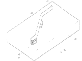
At first electric contacts that is used for testing electronic devices according to the present invention, as shown in figure 26, the end of electronic component 100 (unnumbered) links to each other with the third part 108 of electric contacts 106 header portions by protruding media 102 and by coupling part 104, and electronic component 100 for example is the printed circuit board (PCB) that has predetermined circuit patterns on it.
At this moment, the header portion that electric contacts 106 has possesses the multi-ladder configuration, and this configuration comprises the first bar shaped part 112; Link to each other with first 112, width is greater than the second bar shaped part 110 of first 112; And link to each other with second portion 110, width is greater than the 3rd bar shaped part 108 of second portion 110.
First's 112 free ends of header portion are whole to be connected with tip portion 114, and this tip portion contacts by constant physical force and semiconductor chip pad.
Here, tip portion 114 has butt quadrangular configuration, and has distal end surface rounded.On the OD characteristic, the length of tip portion 114 extends to 30 μ m~500 μ m.In this preferred embodiment, tip portion length is 100 μ m.
Therefore,, when tip portion 114 contacts with the pedestal of semiconductor chip repeatedly, can prevent tip portion 114 wearing and tearing, prevent that himself from producing particle because the tip portion 114 of electric contacts 106 has the quadrangular configuration, and has distal end surface rounded.
Simultaneously, because the end surface of tip portion 114 is slick and sly, when the tip portion 114 of electric contacts 106 contacts with the pedestal of semiconductor chip repeatedly by constant physical force, can prevent the oxide-film that forms on tip portion 114 perforate base, prevent to damage pedestal, thereby can prevent that defective proportion increases when carrying out such as follow-up semiconductor fabrications such as wire bonds processes.
In addition, because the end surface of tip portion 114 is slick and sly, the contact area between tip portion 114 and the semiconductor chip pad increases, and can improve conductivity.
And, because the length of tip portion 114 is 30 μ m~500 μ m, in this embodiment preferred 100 μ m, therefore be easy to adjust the OD characteristic.
In addition, because the header portion of electric contacts 106 has the configuration of multi-ladder, therefore can meet nearest trend, i.e. the trend that spacing diminishes in highly integrated semiconductor device, multi-ladder configuration wherein comprises the first bar shaped part 112 that links to each other with tip portion 114; Link to each other with first 112, width is greater than the second bar shaped part 110 of first 112; And link to each other with second portion 110, width is greater than the 3rd bar shaped part 108 of second portion 110.
That is to say that as shown in figure 34, from third part 108 to first 112, the width of header portion reduces, therefore many electric contacts 106 can radioactively be adjacent to each other, and contact with the pedestal 300 of semiconductor device.This mode meets nearest trend, i.e. the trend that spacing diminishes in highly integrated semiconductor device.
Figure 27 be explanation according to first embodiment of the present invention, be used for the perspective view of second electric contacts that the method for electric contacts of detection. electronics makes by manufacturing.
As shown in figure 27, second electric contacts 115 of the present invention is characterised in that: the tip portion 114 of first electric contacts 106 replaces with tip portion 116, the end that this tip portion forms projection 118 near-ends and has column-shaped configuration and have distal end surface rounded at its near-end.
Here, on the OD characteristic, the length of tip portion 116 extends to 30 μ m~500 μ m.In this preferred embodiment, tip portion 116 length are 100 μ m.
Owing near the near-end of the tip portion 116 of second electric contacts 115, form projection 118, therefore except the working effect that obtains by first electric contacts 106, when tip portion 116 contacts by constant physical force and semiconductor chip pad, the stress that is applied to tip portion 116 near-ends can be disperseed, prevent tip portion 116 fractures.
Figure 28 be explanation according to first embodiment of the present invention, be used for the perspective view of the 3rd electric contacts that the method for electric contacts of detection. electronics makes by manufacturing.
In the 3rd electric contacts 120 of the present invention, the header portion of first electric contacts 106 replaces with has the header portion of configuration in a zigzag.In other words, as shown in figure 28, this header portion has the first bar shaped part 122; The zigzag second portion 124 that links to each other with first 122; And the 3rd bar shaped part 126 that links to each other with second portion 124.
At this moment, the angle of bend of the second zigzag part 124 of header portion is 30 °~170 °, preferred about 90 °.It should be noted that second portion 48 is crooked one or many in a zigzag.
In flexuose header portion since from projection 102 position to tip portion 114, width reduces, and therefore can produce header portion in this way, thereby meet nearest trend easily, be i.e. the trend that spacing diminishes in highly integrated semiconductor device.
The result, because the header portion of the 3rd electric contacts 120 has configuration in a zigzag, therefore except the working effect that first electric contacts 106 is obtained, when tip portion 114 contacts by constant physical force and semiconductor chip pad, because the length from projection 102 to header portion between the tip portion 114 increases, the stress that is applied on the crossbeam can be disperseed, thereby prevent header portion because concentrated the applying of stress ruptured.
Figure 36 is that expression simulation is applied to and is used for the figure of stress distribution of bar shaped header portion of conventional electric contacts of detection. electronics; Figure 37 is that expression simulation is applied to the figure according to the stress distribution of the zigzag header portion of the electric contacts that is used for detection. electronics of the present invention;
With reference to Figure 36 and 37,, on the position of the about 0.4mm of distance projection on the crossbeam, apply and reach 500 * 10 for conventional bar shaped header portion
6The severe stress of Pa.For zigzag header portion of the present invention, can prove conclusively stress and be evenly distributed on the whole zone of header portion.
In addition, from Figure 35, can be readily seen that, because the 3rd electric contacts with header portion of configuration in a zigzag reduces from the width of protruding 102 positions to the position of tip portion 114, can easily meet nearest trend, i.e. the trend that spacing diminishes in highly integrated semiconductor device.
That is to say that because from first 122 to third part 126, the width of header portion reduces, as shown in figure 35, a plurality of electric contacts 120 can be mutually radioactively in abutting connection with arranging, so that contact with the pedestal 302 of semiconductor device.Can meet nearest trend in this way, the trend that spacing diminishes in the promptly highly integrated electronic installation.
Figure 29 be explanation according to first embodiment of the present invention, be used for the perspective view of the 4th kind of electric contacts that the method for electric contacts of detection. electronics makes by manufacturing.
The 4th kind of electric contacts 121 of the present invention is characterised in that: the header portion of first electric contacts 106 replaces with has the in a zigzag header portion of configuration, and this header portion has the first bar shaped part 122, the two the second zigzag parts 124 that link to each other with first and the 3rd bar shaped part 126 that links to each other with second portion 124.The 4th kind of electric contacts 121 features also are: provide tip portion 116 on the third part 126, this tip portion has the near-end that forms projection 118 on every side, and the end that has column-shaped configuration and have distal end surface rounded.
Therefore, the 4th kind of electric contacts 121 can be realized the working effect that the tip portion 116 by second electric contacts 115 is obtained and the working effect that header portion obtained of the 3rd electric contacts 120 simultaneously.
Hereinafter will describe method in detail according to the electric contacts of the second embodiment production test electronic installation of the present invention.
Figure 12 to 18b is a sectional view, and these figure are used to explain the method according to the electric contacts of the second embodiment production test electronic installation of the present invention.
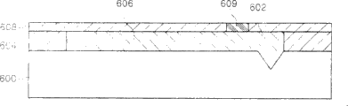
In the method for the embodiment of the present invention, at first, as shown in figure 12, on the whole surface of the sacrificial substrate of making by the silicon (100) of fixed orientation 60, form first diaphragm with predetermined thickness.First diaphragm comprises film and the oxide-film such as photoresist.By carrying out and the identical photoetching process of above-mentioned first embodiment, define second open region (unnumbered), the first diaphragm pattern 62 bigger than first open region in first embodiment.
Then, by using the first diaphragm pattern 62 to implement first etching process as etching mask.Sacrificial substrate 60 is carried out anisotropic etching, and to limit groove 64, this groove has the polygon prismatic configuration of butt, or has the frustum of a cone configuration.Groove 64 laterally inclined has predetermined angle.
At this moment, first etching process that sacrificial substrate 60 is carried out isotropic etching comprises the wet etch process that adopts the chemicals that comprises potassium hydroxide (KOH) etc. to carry out.
Then, as shown in figure 13, remove after the ground floor diaphragm pattern 62, form the second layer diaphragm with predetermined thickness on the whole surface of sacrificial substrate 60, this film comprises film such as photoresist, oxide-film etc.On this film, by carrying out and forming the identical photoetching process of the first diaphragm pattern, 62 situations, form the second diaphragm pattern 66, thereby make the two side ends sealing of groove 64, the middle body that has only groove 64 is open.
Subsequently, shown in Figure 14 a, carry out second etching process as etching mask, further add deep trench 64 by adopting the second diaphragm pattern 66.
At this moment, second etching process comprises that the employing chemicals carries out wet etching, and potassium hydroxide in the chemicals (KOH) mixes with predetermined ratio mutually with deionized water.When adopting chemicals to implement wet etching, groove 64 is able to anisotropically etching, and to determine groove 68, this groove has the polygon prismatic or conical butt configuration of butt, thereby groove 68 is further deepened.
In addition, shown in Figure 14 b, second etching process comprises the wet etch process that adopts chemicals to carry out, hydrogen fluoride in this chemicals (HF), nitric acid (HNO
3) and acetic acid (CH
3COOH) with predetermined mixed.By adopting chemicals to implement wet etching, groove 64 is able to isotropically etching, and to determine groove 70, this groove has column-shaped configuration, and has slick and sly bottom surface.
At this moment, near below the upper end of second open region and the second diaphragm pattern 66, sacrificial substrate 60 is carried out isotropic etching.
Then, shown in Figure 15 a, use the second diaphragm pattern 66 that is coated on the sacrificial substrate 60, wherein limit this pattern with groove 68 with truncated pyramid-shaped configuration by second etching process as etching mask.Under this state, carry out the 3rd etching process once more.
At this moment, the 3rd etching process comprises the RIE process identical with first embodiment well known in the art.By carrying out the 3rd etching process, further increased the degree of depth by the formed groove 68 of second etching process.It should be noted that the 3rd etching process can carry out one or many.
Particularly, in the mode identical, make trench bottom surfaces become slick and sly with the polygon pyramid-shaped configuration of butt or frustum of a cone configuration with first embodiment.
Simultaneously, shown in Figure 15 b, use the second diaphragm pattern 66 that is coated on the sacrificial substrate 60, wherein limit this pattern with groove 70 with frustum of a cone configuration and bottom surface slyness by second etching process as etching mask.Under this state, carry out the 3rd etching process once more.
At this moment, the 3rd etching process comprises the RIE process identical with first embodiment well known in the art.By carrying out the 3rd etching process, further increased the degree of depth, thereby be limited to the cylindricality groove 70 that its near-end has depression by the formed groove 70 of second etching process.
Here, it should be noted that the 3rd etching process can carry out one or many.
Then; shown in Figure 16 a; remove the second diaphragm pattern 66 (a) afterwards referring to Figure 15; on the whole surface of the sacrificial substrate 60 that groove 68 is limited, form the 3rd diaphragm pattern 72 by the 3rd etching process; this pattern comprises the photoresist of predetermined thickness; and limiting the 3rd open region (unnumbered), groove wherein has the polygon prismatic or conical butt configuration of butt, and the bottom surface slyness.Scheme as an alternative; shown in Figure 16 b; remove the second diaphragm pattern 66 (referring to Figure 15 b) afterwards; on the whole surface of the sacrificial substrate 60 that groove 70 is limited, form the 3rd diaphragm pattern 72 by the 3rd etching process; this pattern comprises the photoresist of predetermined thickness; and limiting the 3rd open region (unnumbered), groove 70 wherein has the column-shaped configuration of near-end depression.
At this moment, can used same procedure form the 3rd diaphragm pattern 72 when forming the second diaphragm pattern 66.The formation of the 3rd diaphragm pattern 72 can limit the 3rd open region on sacrificial substrate 60, thereby header portion is formed in the 3rd open region, and the 3rd open region communicates with groove 68,70 respectively.
Subsequently, shown in Figure 17 a, by carrying out CVD, PVD or coating process, electric conducting material 73 is filled into after the 3rd open region that the 3rd diaphragm pattern limited the upper surface of leveling products obtained therefrom with the amount of predetermined thickness on sacrificial substrate 60.Scheme as an alternative; shown in Figure 17 b; by carrying out CVD, PVD or coating process, electric conducting material 74 is filled into after the 3rd open region that the 3rd diaphragm pattern 72 limited the upper surface of leveling products obtained therefrom with the amount of predetermined thickness on sacrificial substrate 60.
At this moment, electric conducting material 73 and 74 is made by nickel alloy etc., can pass through the upper surface leveling of methods such as CMP, deep etch (etchback) and grinding with electric conducting material 73 and 74 products obtained therefroms.
Then, shown in Figure 18 a, along with the 3rd diaphragm pattern 72 from through the removing of sacrificial substrate 60 upper surfaces of screed step, the mode that forms header portion 76 makes it link to each other with tip portion.Scheme as an alternative shown in Figure 18 b,, forms header portion 78 and also it is linked to each other with tip portion when removing through sacrificial substrate 60 upper surfaces of screed step at the 3rd diaphragm pattern 72.
At this moment, by adopting chemicals to carry out wet etch process and removing the 3rd diaphragm pattern such as the dry etching process of ashing etc.
In the mode identical with first embodiment, header portion 76 and 78 each all have the multi-ladder configuration, this configuration comprise first bar shaped part that links to each other with each tip portion of forming in the groove 68 and 70, width greater than second bar shaped of first partly and width greater than the 3rd bar shaped part of second portion.Alternatively, header portion 76 and 78 each all have in a zigzag configuration, this configuration comprises that first bar shaped part, second that links to each other with each tip portion of forming in the groove 68 and 70 is in a zigzag partly and the 3rd bar shaped part.
Equally, the same with first embodiment, carry out a process, by protruding media and by connecting, make the header portion 76,78 that forms on the sacrificial substrate 60 with its on have a required circuit pattern electronic component link to each other.Then, remove sacrificial substrate 60 by methods such as wet etchings, the electric contacts that is used for testing electronic devices promptly is accomplished.
Hereinafter, with the electric contacts of describing in detail according to second embodiment of the present invention that the production method of electric contacts of testing electronic devices produces that is used for.
To be explanation second embodiment according to the present invention be used for the perspective view of the 5th electric contacts that the method for electric contacts of detection. electronics makes by manufacturing to Figure 30.
In the present invention is used for the 5th electric contacts 206 of testing electronic devices, with with the same procedure of first electric contacts 106, as shown in figure 30, the end of electronic component 200 (unnumbered) links to each other with electric contacts 206 by protruding media 202 and by coupling part 204, and electronic component 100 for example is the printed circuit board (PCB) that has predetermined circuit patterns on it.
At this moment, electric contacts 206 has the header portion of multi-ladder configuration, and this configuration comprises the first bar shaped part 212; Link to each other with first 212, width is greater than the second bar shaped part 210 of first; And link to each other with second portion 210, width is greater than the 3rd bar shaped part 208 of second portion 210.
Particularly, can be readily seen that from Figure 30, the 5th kind of electric contacts 206 is characterised in that among the present invention: tip portion 215 integral body are provided at the free end of the 3rd bar shaped part of header portion, contact by constant physical force and semiconductor chip pad, near having, tip portion 215 forms the near-end of projection 214 and the end that has the four prism type configuration and have distal end surface rounded.
At this moment, because the OD characteristic, the length of tip portion 212 extends to 30 μ m~500 μ m.In this preferred embodiment, tip portion length is 100um.
Therefore, except the working effect that obtains by first electric contacts, in the 5th kind of electric contacts 206, when the pedestal of electric contacts 206 by constant physical force and semiconductor chip contacts, because the existence of projection (projection) 214, the stress that is applied to tip portion 215 near-ends might be disperseed, in case tip portion 215 fractures.
Figure 31 be explanation according to second embodiment of the present invention, be used for the perspective view of the 6th kind of electric contacts that the method for electric contacts of detection. electronics makes by manufacturing.
The 6th kind of electric contacts feature of the present invention is: the tip portion 215 of the 5th kind of above-mentioned electric contacts 206 replaces with tip portion 216, wherein first projection forms around near-end, second projections that link to each other with first projection 220, area of section are littler than first projection 220 form at the mid portion of tip portion 216, link to each other with second projection 218, area of section has column-shaped configuration less than the end of second projection 218, its end surface slyness.
Therefore, in the 6th kind of electric contacts 207, because the existence of first projection 220 and second projection 218, when electric contacts 207 contacts with semiconductor chip pad by constant physical force, might more effectively the stress that is applied to tip portion 216 near-ends be disperseed, in case tip portion 216 fractures.
Figure 32 be explanation according to second embodiment of the present invention, be used for the perspective view of the 7th kind of electric contacts that the method for electric contacts of detection. electronics makes by manufacturing.
The 7th kind of electric contacts 230 features of the present invention are: the header portion of the 5th kind of above-mentioned electric contacts 206 replaces with and is the in a zigzag header portion of configuration, and it has second zigzag part 234 that the first bar shaped part 232 links to each other with first 232 and the 3rd bar shaped part 236 that links to each other with second portion 234.
Therefore, because the 7th kind of electric contacts 230 that forms has configuration in a zigzag, except the working effect that obtains by first electric contacts, when tip portion contacts with semiconductor chip pad by constant physical force, the stress that is applied to header portion might be disperseed, in case the tip portion fracture.
Figure 33 be explanation according to second embodiment of the present invention, be used for the perspective view of the 8th kind of electric contacts that the method for electric contacts of detection. electronics makes by manufacturing.
The 7th kind of electric contacts 230 features of the present invention are: the header portion of the 5th kind of above-mentioned electric contacts 206 replaces with the header portion of the word configuration that is, it has the first bar shaped part 232, second zigzag part 234 that links to each other with first 232 and the 3rd bar shaped part 236 that links to each other with second portion 234, and the tip portion 215 of the 5th kind of above-mentioned electric contacts 206 replaces with tip portion 216, wherein first projection forms around near-end, link to each other with first projection 220, area of section forms at the mid portion of tip portion 216 than first projection, the 220 second little projections, link to each other with second projection 218, area of section has column-shaped configuration less than the end of second projection 218, and its end surface slyness.
Therefore, by the 8th kind of electric contacts 231, might realize working effect simultaneously by the header portion of the working effect of the tip portion 216 of the 6th kind of electric contacts 207 and the 7th kind of electric contacts 234.
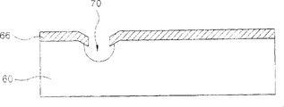
Figure 19 to 25b is a sectional view, and these figure have explained that the 3rd embodiment production according to the present invention is used for the method for the electric contacts of testing electronic devices.
In the method for third embodiment of the invention, at first as shown in figure 19, first diaphragm with predetermined thickness forms on the whole surface of sacrificial substrate 80, and wherein sacrificial substrate 80 is made by the silicon that has such as the fixed orientation of (100).First diaphragm comprises such as the film of photoresist and oxide-film.By carry out with above-mentioned first embodiment in identical photoetching process, formed the first diaphragm pattern 82, this diaphragm pattern has second open region (unnumbered) bigger than first open region in first embodiment.
Then, by carrying out first etching process with the first diaphragm pattern 82 as etching mask, sacrificial substrate 80 is isotropically carried out etching, form the groove 84 with cubic hole configuration, tip portion will form in this groove.
At this moment, first etching process comprises that the employing chemicals carries out wet etching, hydrogen fluoride in the chemicals (HF), nitric acid (HNO
3) and acetic acid (CH
3COOH) with predetermined mixed.
Then, as shown in figure 20, remove the first diaphragm pattern after, on the whole surface of sacrificial substrate 80, form second diaphragm with predetermined thickness, this film comprises film, the oxide-film such as photoresist, or the like.By carrying out identical photoetching process used when forming the first diaphragm pattern 82, form the second diaphragm pattern 86, make the two-side-ends part closure of groove 84, the middle body that has only groove 84 is open.
As Figure 21 a shown in, by with second diaphragm pattern 86 as etching mask carry out second etching process, groove 84 further deepened thereafter.
At this moment, second etching process comprises that the employing chemicals carries out wet etching, and potassium hydroxide in the chemicals (KOH) and deionized water are with predetermined mixed.By adopting this chemicals to carry out wet etch process, groove 84 is carried out anisotropic etching, to determine groove 88, it has the polygon prismatic or conical butt of butt, thereby makes groove 84 darker.
In addition, shown in Figure 21 b, first etching process comprises that the employing chemicals carries out wet etching, hydrogen fluoride in the chemicals (HF), nitric acid (HNO
3) and acetic acid (CH
3COOH) with predetermined mixed.By adopting this chemicals to carry out wet etch process, groove 84 is carried out isotropic etching, to determine groove 90, it has the column configuration, this column configuration near-end depression, and the bottom surface becomes slick and sly.
At this moment, near the upper end of second open region, below the second diaphragm pattern, sacrificial substrate is carried out isotropic etching.
Then, shown in Figure 22 a, use the second diaphragm pattern 86 that is coated on the sacrificial substrate 80, wherein have groove 88 these patterns of qualification of truncated pyramid-shaped configuration by second etching process, usefulness as etching mask.Under this state, implement the 3rd etching process once more.
At this moment, the 3rd etching process comprises used identical RIE method in well known in the art, first embodiment.By the degree of depth of the groove 88 that carries out the 3rd etching process, further increased being limited by second etching process, and the bottom surface of groove 88 becomes slick and sly.
Here, it should be noted that the 3rd moment process can be carried out one or many.
Equally, shown in Figure 22 b, use the second diaphragm pattern 86 that is coated on the sacrificial substrate, wherein have groove 90 these patterns of qualification of truncated pyramid-shaped configuration by second etching process, usefulness as etching mask.Under this state, carry out the 3rd etching process once more.
At this moment, the 3rd etching process comprises used identical RIE method in well known in the art, first embodiment.By the degree of depth of the groove 90 implementing the 3rd etching process, further increased to limit, thereby formed the column groove 90 of near-end depression by second etching process.It should be noted that the 3rd etching process can carry out one or many.
Then; shown in Figure 23 a; after removing the first diaphragm pattern 86; on the whole surface of sacrificial substrate 80, form the second diaphragm pattern 92 with predetermined thickness; it comprises the photoresist with predetermined thickness and defines the 3rd open region (unnumbered), and wherein the groove 88 of sacrificial substrate 80 usefulness with the polygon pyramid-shaped configuration of butt or conical butt configuration limits.Scheme as an alternative; shown in Figure 23 b; after removing the second diaphragm pattern 86; comprise the predetermined thickness photoresist and define the whole surface formation of the 3rd diaphragm pattern 92 of the 3rd open region (unnumbered) in sacrificial substrate 80, wherein the groove 90 of the column configuration of sacrificial substrate 80 usefulness near-end depressions is limited.
At this moment, form the 3rd diaphragm pattern, on sacrificial substrate 80, limit the 3rd open region, make in the 3rd open region and form header portion, the 3rd open region is communicated with groove 88 and 90 respectively.
Subsequently, shown in Figure 24 a, after implementing CVD, PVD or coating process, in the 3rd open region that on sacrificial substrate 80, limits toward the 3rd diaphragm pattern 92, behind the amount filled conductive material 93 with predetermined thickness, flatten the upper surface of products obtained therefrom.Scheme as an alternative, shown in Figure 24 b, by carrying out CVD, PVD or coating process, in the 3rd open region that on sacrificial substrate 80, limits toward the 3rd diaphragm pattern 92, behind the amount filled conductive material 94 with predetermined thickness, the upper surface of leveling products obtained therefrom
At this moment, electric conducting material 93 and 94 is made by nickel alloy etc., the products obtained therefrom upper surface leveling that can will be formed by electric conducting material 93 and 94 by methods such as CMP, deep etch and grindings.
Then; shown in Figure 25 a, when removing the 3rd diaphragm pattern 92, form header portion 96 through sacrificial substrate 80 upper surfaces of flattening course; make it be connected with tip portion, this tip portion has formed two projections continuously near its near-end.Scheme as an alternative, shown in Figure 25 b, from remove the 3rd diaphragm pattern 92 through sacrificial substrate 80 upper surfaces of flattening course after, header portion 98 forms, and makes it be connected with the tip portion with two projections.
At this moment, by adopting chemicals to carry out wet etch process and removing the 3rd diaphragm pattern such as the dry etching process of ashing etc.
By the mode identical with first embodiment, header portion 96 and 98 has the configuration of many levels (multi-step) separately, and this configuration comprises first bar shaped part, width second bar shaped part and width than the second portion big three bar shaped part bigger than first that is connected with each tip portion of formation in groove 88 and 90.Scheme as an alternative, header portion 96 and 98 have configuration in a zigzag separately, and this configuration comprises first bar shaped part, second zigzag part and the 3rd bar shaped part that is connected with each tip portion of formation in groove 88 and 90.
Equally, the same with above-mentioned first embodiment, carry out a process, come by protruding media (medium of abump) and by in conjunction with making on the sacrificial substrate 80 header portion 96 that forms and 98 and realized on it that electronic component of required circuit pattern links.Then, remove sacrificial substrate 80, promptly finish the electric contacts that is used for testing electronic devices by wet etching etc.
Figure 38 a and 38b are respectively explanations according to the sectional view and the perspective view of electric contacts that is used for detection. electronics of the 4th embodiment of the present invention.
In electric contacts according to the embodiment of the present invention, shown in Figure 38 a and 38b, realized the end of electronic component 20 predetermined circuit patterns, such as PCB on it, interconnect with the uprights branch that comprises the projection that pre-determines size.By welding, soldering, plated film, electroconductive binder etc., the header portion with tip portion 26 24 that forms at the one end is connected with column part 22.
At this moment, header portion 24 has configuration in a zigzag, and this configuration has at least one zig-zag type part.On the surface of the zigzag of header portion 24 part, provide armrest 30 of the present invention, this surface from tip portion 26 farthest, thereby make armrest 30 in the horizontal direction near tip portion 26.
In addition, in order to prevent to produce static, on the outer surface of armrest 30, further apply the insulating coating of making by polyimides, parylene etc. 34 owing to contacting between armrest 30 and the electronic component 20.
Hereinafter, being used for the header portion of electric contacts of testing electronic element among the present invention will describe in detail to Figure 41 (f) with reference to Figure 41 (a).
Shown in Figure 41 (a), the header portion 24 of electric contacts has configuration in a zigzag among the present invention, and the first bar shaped part 100, second portion 102 and the third part 104 that wherein have predetermined length are crooked at a predetermined angle, form two bending sections.
At this moment, providing an armrest 106, in the free end of third part 104 part 108 that tapers off to a point near the second portion 102 and the header portion surface between the third part 103 of bending point.
In addition, to shown in 41 (f), the header portion 24 of electric contacts has configuration in a zigzag, the first 110,120,130,140 and 150 of wherein bar shaped among the present invention as Figure 41 (b); Second portion 112,122,132,142 and 152; Third part 114,124,134,144 and 154; Form three bending sections with the 4th part 116,126,136,146 and 156 with predetermined angular bend.
At this moment, near the second portion 112,122,132,142 of bending point and 152 and third part 114,124,134,144 and 154 between the header portion surface armrest 118,128,138,148 and 158 is provided.Free end in the 4th part 116,126,136,146 and 156 part 119,129,139,149 and 159 that tapers off to a point.
At this moment, from Figure 41 (f), obviously as can be seen,, therefore may meet nearest development trend, the i.e. trend that spacing diminishes in highly integrated semiconductor device effectively because header portion 24 is assigned to tip portion 159 its width from uprights and reduced.
That is to say because header portion reduces from four its width of part of third part to the, formed a plurality of header portions 24 with tip portion can emissivity mutually near adjacency, contact with the pedestal of semiconductor device.In this way, can meet nearest development trend, i.e. the trend that spacing diminishes in highly integrated semiconductor device.
As a result, the tip portion 26 of electric contacts contacts by constant physical force and semiconductor chip pad, when having required OD characteristic, applies a constant signal of telecommunication to semiconductor chip, thereby confirms that normally whether semiconductor chip.
At this moment, make header portion 24 bendings by physical force, thereby tip portion 26 is contacted with semiconductor chip pad, header portion 24 surfaces are gone up the armrest 30 that forms and are contacted with electronic component 20.
In addition, when tip portion 26 and semiconductor chip pad are in contact with one another, because header portion 24 has the configuration of crooked one or many in a zigzag, provide armrest 30 on a surface of header portion, phenomenon therefore twists.Because this torsion phenomenon, the pressure that tip portion 26 is applied on the semiconductor chip can double, thereby guarantees that tip portion 26 contacts by oxide-film and semiconductor pedestal reliably.
Figure 39 a and 39b are respectively explanations according to the sectional view and the perspective view of electric contacts that is used for testing electronic devices of the 5th embodiment of the present invention.
Can easily go out from Figure 39 a and 39b, constructing electronics contact element in the embodiment of the present invention with the 4th mode that embodiment is identical, difference is to provide armrest 50 on the electronic component 40 with on the corresponding position of sweep near the header portion 44 of tip portion 46.
At this moment, owing to producing static, the contact between armrest 50 and the header portion 44 on the outer surface of armrest 50, further applies an insulating coating 52 of making by polyimides, Parylene etc. in order to prevent.
As a result, the tip portion 46 of electric contacts contacts with semiconductor chip pad by constant physical force, when having required OD characteristic, applies a constant signal of telecommunication to semiconductor chip, thereby confirms that normally whether semiconductor chip.
At this moment, make header portion 44 bendings, thereby tip portion 46 is contacted with semiconductor chip pad, the armrest 50 that forms on the electronic component 40 is contacted with a surface of header portion 44 by physical force.
In addition, when tip portion 46 and semiconductor chip pad were in contact with one another, because header portion 44 has the configuration of crooked one or many in a zigzag and armrest 50 is provided on electronic component, phenomenon therefore twisted.Because this torsion phenomenon, the pressure that tip portion 46 is applied on the semiconductor chip can double, thereby guarantees that tip portion 46 contacts with the semiconductor pedestal by oxide-film reliably.
To be respectively explanation be used for the sectional view and the perspective view of electric contacts of detection. electronics according to the manufacturing of the 6th embodiment of the present invention for Figure 40 a and 40b.
From Figure 40 a and 40b as can be seen, be used for the electronics contact element of testing electronic devices in the embodiment of the present invention to construct with the 4th mode that embodiment is identical, difference be a pair of armrest 70 and 74 1 levels near tip portions 26 on the zigzag part surface of header portion 64, this surface in vertical direction farthest from tip portion 66, another on the electronic component 40 with the sweep corresponding position of level near the header portion of tip portion 46 on.
At this moment, the armrest that lays respectively on header portion 64 and the electronic component 60 has at interval to each other to 70 and 74, depends on the degree of crook of header portion 64.In order to prevent to produce static, on the outer surface of armrest 70 and 74, further apply the insulating coating of making by polyimides, Parylene etc. 72 and 76 owing to contacting between armrest 70 and 74.
As a result, the tip portion 66 of electric contacts contacts by constant physical force and semiconductor chip pad, when having required OD characteristic, provides a constant signal of telecommunication to semiconductor chip, thereby confirms that normally whether semiconductor chip.
At this moment, make header portion 64 bendings by physical force, in this way, tip portion 66 and semiconductor chip pad contact, and header portion 64 lip-deep armrests contact with electronic component 60 to 70 and 74.
In addition, when tip portion 66 and semiconductor chip pad are in contact with one another,, providing armrest 70 and 74 on the surface of header portion He on the electronic component because header portion 64 has the configuration of crooked one or many in a zigzag, so the phenomenon that twists.Because this torsion phenomenon, the pressure that tip portion 66 is applied on the semiconductor chip can double, thereby guarantees that tip portion 66 contacts with the semiconductor pedestal by oxide-film reliably.
Figure 42 a to 42i is a sectional view, and this figure has explained the production method of electric contacts shown in Figure 38 a and the 38b, that be used for testing electronic devices.
In the method for the embodiment of the present invention, at first, shown in Figure 42 a, on the whole surface of the sacrificial substrate of making by silicon 200, form first diaphragm of predetermined thickness.First diaphragm can comprise the film such as photoresist etc.Then, by making the first diaphragm patterning, form the first diaphragm pattern 202, make the first diaphragm pattern 202 can limit first open region, tip portion forms in this open region.
At this moment, in rotation sacrificial substrate 200, by the coating photoresist, expose and make development such as photoresist, on sacrificial substrate, form the first diaphragm pattern 202 that comprises photoresist etc.
Then, shown in Figure 42 b, carry out etching process by using the first diaphragm pattern 202 as etching mask, limit groove 204 on sacrificial substrate 200, part tapers off to a point in this groove in the subsequent process.
At this moment, the etching process of qualification groove 204 comprises that the employing chemicals carries out wet etching, perhaps adopts reacting gas to carry out dry etching.After limiting groove 204, by in groove, carrying out the one or many anisotropic etching, increase the degree of depth of groove 204, thereby make groove 204 have the polygon prismatic or conical butt configuration of butt, wherein have the side of inclination.Equally, become slick and sly and in groove, carry out the one or many anisotropic etching, form slick and sly tip portion 218 by the inner surface that makes groove 204.
Then; shown in Figure 42 c; after by removal first diaphragm patterns 202 such as ashing; form the second diaphragm pattern 206 to limit second open area; in second open area, form crooked one or many in a zigzag and have the header portion of at least one sweep, and second open area communicates with flute 204.
At this moment, the mode with identical with the first diaphragm pattern 202 forms the second diaphragm pattern 206 by applying photoresist, exposure and development continuously.
Then; shown in Figure 42 d, on sacrificial substrate 200, form after the second diaphragm pattern, by carrying out CVD, PVD or coating process; in second open region of the second diaphragm pattern 206, form the electric conducting material 208 of predetermined thickness, form header portion and tip portion in this way.Subsequently, the upper surface of leveling products obtained therefrom.Then; shown in Figure 42 e; on the whole surface of the sacrificial substrate 200 of passing through flattening course, form the 3rd diaphragm pattern 210; thereby limit the 3rd open region; to form an armrest therein in the subsequent process, armrest position level is near the groove 204 of the part that will taper off to a point therein.
At this moment, form the 3rd diaphragm pattern 210, to guarantee in the subsequent process forming armrest on the crooked position of the header portion of the crooked one or many of the zigzag that will form, wherein the sweep of header portion is near tip portion.
Then, shown in Figure 42 f, on sacrificial substrate 200, form after the 3rd diaphragm pattern 210,, in the 3rd open region of the 3rd diaphragm pattern 210, form the electric conducting material 211 of predetermined thickness by carrying out CVD, PVD or coating process.Subsequently, the upper surface of leveling products obtained therefrom.
At this moment, can pass through of the upper surface leveling of methods such as CMP, deep etch and grinding with the products obtained therefrom of electric conducting material 211 formation.
Subsequently, shown in Figure 42 g,, form header portion 214 and armrest 212 by removing the second diaphragm pattern 206 and the 3rd diaphragm pattern 210.Be applied on the outer surface of armrest 212 by the insulating coating of making such as megohmite insulants such as polyimides, Parylenes 216.
Then, shown in Figure 42 h, realized on it that end of electronic component 300 predetermined circuit patterns, such as PCB forms column (post) part of the projection that comprises pre-sizing.By jockeys 304 such as welding, soldering, plated film, electroconductive binders, header portion 24 ends that form on sacrificial substrate 200 in the prior process are connected with column part 302, wherein the end of header portion 24 is from armrest 212 farthest.
At last, shown in Figure 42 i, remove sacrificial substrate 200 by wet etching, make the header portion freedom, and tip portion 218 is connected with it, the electric contacts that has armrest 212 on the header portion 214 promptly is accomplished.
Figure 43 a to 43d is a sectional view, and these figure have explained the production method of the electric contacts that is used for testing electronic devices shown in Figure 39 a and the 39b.
In the method for fifth embodiment of the invention; shown in Figure 43 a; identical with the production method of electric contacts in the 4th embodiment; the formation of the second diaphragm pattern 404 can limit second open region; in this open region, form crooked one or many in a zigzag, have the header portion of at least one sweep.The groove 402 that forms on the second diaphragm pattern 404 and the sacrificial substrate 400 communicates, and groove 402 limits on sacrificial substrate 400 by using the first diaphragm pattern (not shown) to carry out etching process, and the part that tapers off to a point in groove.
Limit after the groove 402,, increase the degree of depth of groove 402, thereby make groove 402 have the polygon prismatic or conical butt configuration of butt, wherein have the side of inclination by in groove 402, carrying out the one or many anisotropic etching.In addition, become slick and sly, in groove, carry out the one or many anisotropic etching, form slick and sly tip portion 218 by the inner surface that makes groove 204.
Then, on sacrificial substrate 400, form after the second diaphragm pattern 404,, in second open region of the second diaphragm pattern 404, form the electric conducting material 406 of predetermined thickness by carrying out CVD, PVD or coating process.Subsequently, the upper surface of leveling products obtained therefrom.
Then, shown in Figure 43 b,, form the crooked one or many of zigzag, have the header portion 408 of configuration in a zigzag by removing the second diaphragm pattern 404.At this moment, remove the second diaphragm pattern by implementing wet etching etc.
Then, shown in Figure 43 c, realized on it that end of electronic component 500 predetermined circuit patterns, such as PCB forms the armrest 504 with pre-sizing.Be applied on the outer surface of armrest 504 by the insulating coating of making such as megohmite insulants such as polyimides, Parylenes 506.
At this moment, on the locational electronic component 500 of sweep of header portion 408 adjacent on the crooked one or many of zigzag, the horizontal level, form armrest 504 with tip portion.
End at electronic component 500 forms the column part 502 that comprises the projection with pre-sizing.By jockeys 508 such as welding, soldering, plated film, electroconductive binders, make from groove 402 header portion 408 ends farthest to link to each other with column part 502.
At last, shown in Figure 43 d, remove sacrificial substrate 400, thereby header portion 408 freedom and tip portion 410 are contacted with it, made the electric contacts that has armrest 504 on the electronic component 500 by wet etching.
Figure 44 a to 44d is a sectional view, and these figure have explained the production method of the electric contacts that is used for testing electronic devices shown in Figure 40 a and the 40b.
In the method for the 6th embodiment of the present invention; shown in Figure 44 a; identical with the production method of electric contacts in the 4th embodiment; the formation of the second diaphragm pattern 604 can limit second open region; in this open region, form crooked one or many in a zigzag, have the header portion of at least one sweep.The second diaphragm pattern 604 and communicate, and the part that in groove, tapers off to a point by using the first diaphragm pattern (not shown) to carry out the groove 602 that etching process limits on sacrificial substrate 600.
After limiting groove 602, by in groove 602, carrying out the one or many anisotropic etching, increase the degree of depth of groove 602, thereby make groove 602 have the polygon prismatic or conical butt configuration of butt, it has the side of inclination.Simultaneously, become slick and sly, in groove, carry out the one or many anisotropic etching, can form slick and sly tip portion 616 by the inner surface that makes groove 602.
Then, on sacrificial substrate 600, form after the second diaphragm pattern 604,, in second open region of the second diaphragm pattern 604, form electric conducting material 609 with predetermined thickness by implementing CVD, PVD or coating process.Subsequently, the upper surface of leveling products obtained therefrom.
In addition, on the products obtained therefrom that comprises the sacrificial substrate 600 of passing through flattening course, form the 3rd diaphragm pattern 608, thereby limit the 3rd open region, in this open region, form armrest.
At this moment, form the 3rd diaphragm pattern 608, to guarantee on the crooked position of header portion adjacent with tip portion, that in subsequent process, form on the crooked one or many of zigzag, the horizontal direction, forming armrest.
Then, on sacrificial substrate 600, form after the 3rd diaphragm pattern 608,, in the 3rd open region of the 3rd diaphragm pattern 608, form electric conducting material 609 with predetermined thickness by carrying out CVD, PVD or coating process.Subsequently, the upper surface of leveling products obtained therefrom.
Then, shown in Figure 44 b,, form header portion 614 and armrest 610 by removing the second diaphragm pattern 604 and the 3rd diaphragm pattern 608.To be applied on the outer surface of armrest 610 by the insulating coating of making such as megohmite insulants such as polyimides, Parylenes 612.
Then, shown in Figure 44 c, realized that thereon the end of electronic component 700 predetermined circuit patterns, such as PCB forms the armrest 702 with pre-sizing.To be applied on the outer surface of armrest 702 by the insulating coating of making such as megohmite insulants such as polyimides, Parylenes 704.
At this moment, with header portion 614 on form armrest 702 on the armrest 610 corresponding positions that form.
End at electronic component 700 forms the column part 706 that comprises the projection with pre-sizing.By jockeys 708 such as welding, soldering, plated film, electroconductive binders, header portion 614 ends from groove 602 are linked to each other with column part 706.
At this moment, the connected mode of armrest 702 makes it the armrest 610 in the face of formation on the header portion 614, and has at interval with it.
At last, shown in Figure 44 d, remove sacrificial substrate 600, thereby make header portion 614 freedom, and tip portion 616 is attached thereto, made the electric contacts that has armrest 610 and 702 on header portion 614 and the electronic component 700 respectively by wet etching.
Below, will the stress distribution of the header portion that applies the electric contacts that is used for testing electronic devices in the present invention be described with reference to figure 45a and 45b, and the stress distribution that is applied to the header portion of the conventional electric contacts that is used for testing electronic devices.
For the header portion among the present invention, shown in Figure 45 a, apply the constant stress of about 500M (Pa) to header portion by a cross section, separate with jockey in cross section wherein, as 5.0 * 10
-4To 2.0 * 10
-33The projection of m.On the contrary, for the header portion of routine, shown in Figure 45 b, apply the variable stresses of 400M to 500M (Pa) to header portion by identical cross section.
From top description obviously as can be seen, be used for the production method of the electric contacts of testing electronic devices among the present invention, and the electric contacts of producing by this method has following advantage.
In the present invention, because stress is applied to the header portion of electric contacts dispersedly, might make header portion be unlikely to fracture repeatedly contacted the time with semiconductor chip.
In the present invention, because the end of tip portion has the polygon prismatic or conical butt configuration of butt, and has distal end surface rounded; Perhaps has the column configuration, and has a distal end surface rounded, when the tip portion of electric contacts contacts with the pedestal of semiconductor chip repeatedly by constant physical force, the oxide-film that tip portion forms on can perforate base prevents that defective proportion increases when carrying out such as follow-up semiconductor fabrications such as wire bonds.Simultaneously, avoided the end fray of electric contacts and produce the possibility of particle.
In addition, owing to will be slick and sly, have increased the contact area of tip portion, thereby improved its conductivity with the end surface of the contacted electric contacts tip portion of semiconductor pedestal and so on material.
In addition, extend to 30 μ m~500 μ m, be easy to adjust the OD characteristic owing to electrically contact the length of the tip portion of material.Because projection forms around the near-end of tip portion, be connected with each other at this position electric contacts tip portion and header portion, when the tip portion of electric contacts contacts with the pedestal of semiconductor chip repeatedly by constant physical force, this stress is not applied to the near-end of tip portion, and can prevent the tip portion fracture.
In addition, because a plurality of step portion of header portion tool of electric contacts meet nearest trend, i.e. the trend of required pitch smaller in such as highly integrated electronic installations such as semiconductor chip fully.And, because the header portion of electric contacts has configuration in a zigzag, when the tip portion of electric contacts contacts with the pedestal of semiconductor chip repeatedly with constant physical force, the stress that is applied to header portion might be disperseed, make header portion be unlikely to fracture.
In addition, owing to can use and have highly microelectromechanical systems (the micro electro mechanicalsystem of repeatability, MEMS) produce electric contacts of the present invention in enormous quantities, might improve output, productivity ratio and testing of electronic devices kit, as comprise the operating reliability of the probe of electric contacts.
In addition, because the torsional effect that armrest caused might come the measuring semiconductor chip with the physical force that significantly increases to a certain degree, the increase degree of this physical force makes tip portion may pierce through formed oxide-film on the semiconductor pedestal.
In drawing and description, typical preferred embodiment of the present invention is disclosed, though adopted technical term, these terms just use on general and illustrative meaning, the invention scope defined in following claims are not imposed any restrictions.
Claims (10)
1. a manufacturing is used for the method for the electric contacts of test electronic device, and this method comprises:
In sacrificial substrate, form the groove that limits the tip portion shape;
Formation has the crossbeam mask pattern of opening, and described opening limits the shape of header portion and exposes described groove;
Formation has the electric contacts of header portion and tip portion, and described header portion and tip portion lay respectively in described opening and the described groove; With
Remove described sacrificial substrate and described crossbeam mask pattern,
Wherein, the formation of described groove comprises at least one wet etch step and at least one dry etch step; With
The distal portions that described tip portion comprises the proximal part that connects described header portion, extend to the direction that deviates from described proximal part from described proximal part and from the projection of the sidewall horizontal expansion of proximal part, and form described groove to limit the shape of described near-end, far-end and projection.
2. the method for claim 1, wherein said at least one wet etch step utilization comprise that the chemicals of potassium hydroxide implements, and make described far-end have polygon prism shape of butt or frusto-conical.
3. the method for claim 1, wherein said at least one wet etch step utilization comprise that the chemicals of hydrogen fluoride, nitric acid and acetic acid implements, and make described far-end have cylindrical configuration.
4. the method for claim 1, wherein said at least one dry etch step increases the degree of depth of described groove and makes described groove have the round bottom surface.
5. the method for claim 1 wherein forms described opening, makes described header portion comprise the second portion and the third part that is connected second portion of first, connection first, and wherein second portion has sweep.
6. method as claimed in claim 5, wherein said second portion is crooked one or many in a zigzag.
7. method as claimed in claim 5, first, second of wherein said header portion and third part are arranged on the sacrificial substrate that is exposed by described opening, make that the basal surface of described header portion is smooth.
8. the method for claim 1, the formation of wherein said groove comprises:
Form the last groove that limits described proximal part shape, the sidewall that described upward groove has predetermined oblique angle;
The described central basal surface of groove of going up of etching is to form the lower groove that limits described distal portions shape.
9. method as claimed in claim 8, the formation of wherein said groove also are included in to form and go up after the groove, and the described central basal surface of groove of going up of anisotropic etching is to increase the degree of depth of described groove.
10. method as claimed in claim 8 wherein forms the described groove of going up and comprises that utilization comprises the chemicals wet etching of potassium hydroxide so that the described basal surface of going up groove has the polygon prismatic or conical butt configuration of butt.
Applications Claiming Priority (6)
| Application Number | Priority Date | Filing Date | Title |
|---|---|---|---|
| KR1020020006367A KR100358513B1 (en) | 2002-02-05 | 2002-02-05 | Method of fabricating electrical contactor for testing electronic device and electrical contactor fabricated thereby |
| KR20026367 | 2002-02-05 | ||
| KR2002-6367 | 2002-02-05 | ||
| KR10-2002-0068402 | 2002-11-06 | ||
| KR10-2002-0068402A KR100475468B1 (en) | 2002-11-06 | 2002-11-06 | Electric contact element for testing electro device |
| KR1020020068402 | 2002-11-06 |
Related Child Applications (1)
| Application Number | Title | Priority Date | Filing Date |
|---|---|---|---|
| CN2008101355299A Division CN101354405B (en) | 2002-02-05 | 2002-11-08 | Method for manufacturing electrical contact element for testing electro device and electrical contact element thereby |
Publications (2)
| Publication Number | Publication Date |
|---|---|
| CN1618124A CN1618124A (en) | 2005-05-18 |
| CN100423221C true CN100423221C (en) | 2008-10-01 |
Family
ID=36931458
Family Applications (1)
| Application Number | Title | Priority Date | Filing Date |
|---|---|---|---|
| CNB028277597A Expired - Fee Related CN100423221C (en) | 2002-02-05 | 2002-11-08 | Method for manufacturing electrical contact element for testing electro device and electrical contact element thereby |
Country Status (6)
| Country | Link |
|---|---|
| US (2) | US20040018752A1 (en) |
| JP (1) | JP2005517192A (en) |
| CN (1) | CN100423221C (en) |
| AU (1) | AU2002353582A1 (en) |
| DE (1) | DE10297653T5 (en) |
| WO (1) | WO2003067650A1 (en) |
Families Citing this family (30)
| Publication number | Priority date | Publication date | Assignee | Title |
|---|---|---|---|---|
| US7459795B2 (en) * | 2004-08-19 | 2008-12-02 | Formfactor, Inc. | Method to build a wirebond probe card in a many at a time fashion |
| KR100586675B1 (en) * | 2004-09-22 | 2006-06-12 | 주식회사 파이컴 | Manufacture method of vertical-type electric contactor and vertical-type electric contactor thereof |
| KR100585561B1 (en) * | 2004-10-26 | 2006-06-07 | 주식회사 파이컴 | Manufacture method of vertical-type electric contactor and vertical-type electric contactor thereof |
| KR100626570B1 (en) * | 2004-12-24 | 2006-09-25 | 주식회사 파이컴 | A probe card manufacturing method include sensing probe and the probe card, probe card inspection system |
| US7589542B2 (en) * | 2007-04-12 | 2009-09-15 | Touchdown Technologies Inc. | Hybrid probe for testing semiconductor devices |
| US7772859B2 (en) * | 2005-08-01 | 2010-08-10 | Touchdown Technologies, Inc. | Probe for testing semiconductor devices with features that increase stress tolerance |
| US7362119B2 (en) * | 2005-08-01 | 2008-04-22 | Touchdown Technologies, Inc | Torsion spring probe contactor design |
| KR100653636B1 (en) * | 2005-08-03 | 2006-12-05 | 주식회사 파이컴 | Vertical type probe and methods of fabricating and bonding the same |
| KR100664443B1 (en) * | 2005-08-10 | 2007-01-03 | 주식회사 파이컴 | Cantilever type probe and method of fabricating the same |
| TW200739083A (en) | 2005-09-30 | 2007-10-16 | Sv Probe Pte Ltd | Cantilever probe structure for a probe card assembly |
| ITMI20052290A1 (en) * | 2005-11-30 | 2007-06-01 | Pasqua Roberto Della | INSTANTANEOUS MESSAGING SERVICE WITH MINIMIZED USER INTERFACE |
| KR100749735B1 (en) | 2006-06-07 | 2007-08-16 | 주식회사 파이컴 | Method of fabricating cantilever type probe and method of fabricating probe card using the same |
| US20080011476A1 (en) * | 2006-07-11 | 2008-01-17 | Halliburton Energy Services, Inc. | Methods for coating particulates with tackifying compounds |
| US7782072B2 (en) * | 2006-09-27 | 2010-08-24 | Formfactor, Inc. | Single support structure probe group with staggered mounting pattern |
| JP2008151573A (en) * | 2006-12-15 | 2008-07-03 | Micronics Japan Co Ltd | Electrical connection apparatus and its manufacturing method |
| JP4916893B2 (en) * | 2007-01-05 | 2012-04-18 | 株式会社日本マイクロニクス | Probe manufacturing method |
| KR101368139B1 (en) * | 2007-07-16 | 2014-03-12 | 어드밴티스트 아메리카, 인크. | A device and method for repairing a microelectromechanical system |
| JP2009025107A (en) * | 2007-07-19 | 2009-02-05 | Advanced Systems Japan Inc | Manufacturing method of convex form spiral contactor |
| US7589547B2 (en) * | 2007-09-13 | 2009-09-15 | Touchdown Technologies, Inc. | Forked probe for testing semiconductor devices |
| US20090072851A1 (en) * | 2007-09-13 | 2009-03-19 | Touchdown Technologies, Inc. | Multi-Pivot Probe Card For Testing Semiconductor Devices |
| US20090144970A1 (en) * | 2007-12-06 | 2009-06-11 | Winmems Technologies Holdings Co., Ltd. | Fabricating an array of mems parts on a substrate |
| US7811849B2 (en) * | 2008-01-30 | 2010-10-12 | Winmems Technologies Co., Ltd. | Placing a MEMS part on an application platform using a guide mask |
| US20100013060A1 (en) * | 2008-06-22 | 2010-01-21 | Taiwan Semiconductor Manufacturing Company, Ltd. | Method of forming a conductive trench in a silicon wafer and silicon wafer comprising such trench |
| US8089294B2 (en) * | 2008-08-05 | 2012-01-03 | WinMENS Technologies Co., Ltd. | MEMS probe fabrication on a reusable substrate for probe card application |
| US7737714B2 (en) * | 2008-11-05 | 2010-06-15 | Winmems Technologies Holdings Co., Ltd. | Probe assembly arrangement |
| US7928751B2 (en) * | 2009-02-18 | 2011-04-19 | Winmems Technologies Holdings Co., Ltd. | MEMS interconnection pins fabrication on a reusable substrate for probe card application |
| TWI417646B (en) * | 2010-03-29 | 2013-12-01 | Pixart Imaging Inc | Mems lithography mask with improved tungsten deposition topography and method for the same |
| CN102219177A (en) * | 2010-04-14 | 2011-10-19 | 原相科技股份有限公司 | Micro electro mechanical system photomask and method for improving topological appearance of tungsten sediment |
| US10859602B2 (en) * | 2012-03-07 | 2020-12-08 | Advantest Corporation | Transferring electronic probe assemblies to space transformers |
| CN110277437A (en) * | 2018-03-16 | 2019-09-24 | 张峻玮 | A kind of Xiao's based diode structure and its manufacturing method of the high-effect low-leakage current of outer cladding formula |
Citations (7)
| Publication number | Priority date | Publication date | Assignee | Title |
|---|---|---|---|---|
| JPH07333232A (en) * | 1994-06-13 | 1995-12-22 | Canon Inc | Formation of cantilever having probe |
| JPH0850146A (en) * | 1994-06-03 | 1996-02-20 | Hitachi Ltd | Connecting device and its manufacture |
| CN1194692A (en) * | 1996-05-17 | 1998-09-30 | 福姆法克特公司 | Microelectronic tontact structure and method of making same |
| CN1208368A (en) * | 1995-05-26 | 1999-02-17 | 福姆法克特公司 | Fabricating interconnects and tips using sacrificial substrates |
| US6184053B1 (en) * | 1993-11-16 | 2001-02-06 | Formfactor, Inc. | Method of making microelectronic spring contact elements |
| KR20010077628A (en) * | 2000-02-03 | 2001-08-20 | 최성수 | fabrication of sub-wavelength aperture for near field optical sensor |
| US6307392B1 (en) * | 1997-10-28 | 2001-10-23 | Nec Corporation | Probe card and method of forming a probe card |
Family Cites Families (13)
| Publication number | Priority date | Publication date | Assignee | Title |
|---|---|---|---|---|
| US4998062A (en) | 1988-10-25 | 1991-03-05 | Tokyo Electron Limited | Probe device having micro-strip line structure |
| US4916002A (en) * | 1989-01-13 | 1990-04-10 | The Board Of Trustees Of The Leland Jr. University | Microcasting of microminiature tips |
| EP0413041B1 (en) * | 1989-08-16 | 1992-07-15 | International Business Machines Corporation | Method of producing micromechanical sensors for the afm/stm profilometry and micromechanical afm/stm sensor head |
| US5177438A (en) * | 1991-08-02 | 1993-01-05 | Motorola, Inc. | Low resistance probe for semiconductor |
| US6482013B2 (en) * | 1993-11-16 | 2002-11-19 | Formfactor, Inc. | Microelectronic spring contact element and electronic component having a plurality of spring contact elements |
| US5513430A (en) * | 1994-08-19 | 1996-05-07 | Motorola, Inc. | Method for manufacturing a probe |
| WO1997043654A1 (en) * | 1996-05-17 | 1997-11-20 | Formfactor, Inc. | Microelectronic spring contact elements |
| US6307932B1 (en) * | 1998-03-31 | 2001-10-23 | Avaya Technology Corp | End-user control of audio delivery endpoint in a multimedia environment |
| US6414501B2 (en) * | 1998-10-01 | 2002-07-02 | Amst Co., Ltd. | Micro cantilever style contact pin structure for wafer probing |
| US6426638B1 (en) * | 2000-05-02 | 2002-07-30 | Decision Track Llc | Compliant probe apparatus |
| US6970005B2 (en) * | 2000-08-24 | 2005-11-29 | Texas Instruments Incorporated | Multiple-chip probe and universal tester contact assemblage |
| JP2002071719A (en) | 2000-09-01 | 2002-03-12 | Kobe Steel Ltd | Probe card and production method thereof |
| US6811406B2 (en) * | 2001-04-12 | 2004-11-02 | Formfactor, Inc. | Microelectronic spring with additional protruding member |
-
2002
- 2002-11-08 CN CNB028277597A patent/CN100423221C/en not_active Expired - Fee Related
- 2002-11-08 WO PCT/KR2002/002073 patent/WO2003067650A1/en active Application Filing
- 2002-11-08 JP JP2003566894A patent/JP2005517192A/en active Pending
- 2002-11-08 AU AU2002353582A patent/AU2002353582A1/en not_active Abandoned
- 2002-11-08 DE DE10297653T patent/DE10297653T5/en not_active Ceased
-
2003
- 2003-01-23 US US10/350,737 patent/US20040018752A1/en not_active Abandoned
-
2006
- 2006-02-13 US US11/352,658 patent/US7579855B2/en not_active Expired - Fee Related
Patent Citations (7)
| Publication number | Priority date | Publication date | Assignee | Title |
|---|---|---|---|---|
| US6184053B1 (en) * | 1993-11-16 | 2001-02-06 | Formfactor, Inc. | Method of making microelectronic spring contact elements |
| JPH0850146A (en) * | 1994-06-03 | 1996-02-20 | Hitachi Ltd | Connecting device and its manufacture |
| JPH07333232A (en) * | 1994-06-13 | 1995-12-22 | Canon Inc | Formation of cantilever having probe |
| CN1208368A (en) * | 1995-05-26 | 1999-02-17 | 福姆法克特公司 | Fabricating interconnects and tips using sacrificial substrates |
| CN1194692A (en) * | 1996-05-17 | 1998-09-30 | 福姆法克特公司 | Microelectronic tontact structure and method of making same |
| US6307392B1 (en) * | 1997-10-28 | 2001-10-23 | Nec Corporation | Probe card and method of forming a probe card |
| KR20010077628A (en) * | 2000-02-03 | 2001-08-20 | 최성수 | fabrication of sub-wavelength aperture for near field optical sensor |
Also Published As
| Publication number | Publication date |
|---|---|
| DE10297653T5 (en) | 2005-04-14 |
| JP2005517192A (en) | 2005-06-09 |
| US20040018752A1 (en) | 2004-01-29 |
| CN1618124A (en) | 2005-05-18 |
| WO2003067650A1 (en) | 2003-08-14 |
| US20060192581A1 (en) | 2006-08-31 |
| AU2002353582A1 (en) | 2003-09-02 |
| US7579855B2 (en) | 2009-08-25 |
Similar Documents
| Publication | Publication Date | Title |
|---|---|---|
| CN100423221C (en) | Method for manufacturing electrical contact element for testing electro device and electrical contact element thereby | |
| KR100307082B1 (en) | Connection structure of integrated circuit and its manufacturing method | |
| US6400166B2 (en) | Micro probe and method of fabricating same | |
| US6613662B2 (en) | Method for making projected contact structures for engaging bumped semiconductor devices | |
| US7053641B2 (en) | Interconnect having spring contacts | |
| US6651325B2 (en) | Method for forming cantilever beam probe card and probe card formed | |
| US7602204B2 (en) | Probe card manufacturing method including sensing probe and the probe card, probe card inspection system | |
| US6392430B1 (en) | Method of forming coaxial silicon interconnects | |
| KR100523745B1 (en) | Microprobe and Method for Manufacturing the Same Using MEMS and Electroplating Technology | |
| CN101354405B (en) | Method for manufacturing electrical contact element for testing electro device and electrical contact element thereby | |
| KR100586675B1 (en) | Manufacture method of vertical-type electric contactor and vertical-type electric contactor thereof | |
| KR20040048253A (en) | Cantilever-type probe card and method for manufacturing the same using silicon micromachining technology | |
| KR100703043B1 (en) | Probe substrate for test and manufacturing method thereof | |
| KR100475468B1 (en) | Electric contact element for testing electro device | |
| KR100464681B1 (en) | Method for manufacturing tip of electric contactor for testing electro device | |
| KR100463308B1 (en) | Vertical type electrical contactor and method for manufacturing its |
Legal Events
| Date | Code | Title | Description |
|---|---|---|---|
| C06 | Publication | ||
| PB01 | Publication | ||
| C10 | Entry into substantive examination | ||
| SE01 | Entry into force of request for substantive examination | ||
| C14 | Grant of patent or utility model | ||
| GR01 | Patent grant | ||
| C17 | Cessation of patent right | ||
| CF01 | Termination of patent right due to non-payment of annual fee |
Granted publication date: 20081001 Termination date: 20121108 |