CN100438239C - Optical element, and its manufacturing method - Google Patents
Optical element, and its manufacturing method Download PDFInfo
- Publication number
- CN100438239C CN100438239C CNB2004100987965A CN200410098796A CN100438239C CN 100438239 C CN100438239 C CN 100438239C CN B2004100987965 A CNB2004100987965 A CN B2004100987965A CN 200410098796 A CN200410098796 A CN 200410098796A CN 100438239 C CN100438239 C CN 100438239C
- Authority
- CN
- China
- Prior art keywords
- insulating barrier
- layer
- optical element
- cylindrical portion
- reflector
- Prior art date
- Legal status (The legal status is an assumption and is not a legal conclusion. Google has not performed a legal analysis and makes no representation as to the accuracy of the status listed.)
- Expired - Fee Related
Links
Images


Classifications
-
- H—ELECTRICITY
- H01—ELECTRIC ELEMENTS
- H01S—DEVICES USING THE PROCESS OF LIGHT AMPLIFICATION BY STIMULATED EMISSION OF RADIATION [LASER] TO AMPLIFY OR GENERATE LIGHT; DEVICES USING STIMULATED EMISSION OF ELECTROMAGNETIC RADIATION IN WAVE RANGES OTHER THAN OPTICAL
- H01S5/00—Semiconductor lasers
- H01S5/02—Structural details or components not essential to laser action
- H01S5/028—Coatings ; Treatment of the laser facets, e.g. etching, passivation layers or reflecting layers
- H01S5/0282—Passivation layers or treatments
-
- H—ELECTRICITY
- H01—ELECTRIC ELEMENTS
- H01S—DEVICES USING THE PROCESS OF LIGHT AMPLIFICATION BY STIMULATED EMISSION OF RADIATION [LASER] TO AMPLIFY OR GENERATE LIGHT; DEVICES USING STIMULATED EMISSION OF ELECTROMAGNETIC RADIATION IN WAVE RANGES OTHER THAN OPTICAL
- H01S5/00—Semiconductor lasers
- H01S5/02—Structural details or components not essential to laser action
- H01S5/026—Monolithically integrated components, e.g. waveguides, monitoring photo-detectors, drivers
- H01S5/0262—Photo-diodes, e.g. transceiver devices, bidirectional devices
- H01S5/0264—Photo-diodes, e.g. transceiver devices, bidirectional devices for monitoring the laser-output
-
- H—ELECTRICITY
- H01—ELECTRIC ELEMENTS
- H01S—DEVICES USING THE PROCESS OF LIGHT AMPLIFICATION BY STIMULATED EMISSION OF RADIATION [LASER] TO AMPLIFY OR GENERATE LIGHT; DEVICES USING STIMULATED EMISSION OF ELECTROMAGNETIC RADIATION IN WAVE RANGES OTHER THAN OPTICAL
- H01S5/00—Semiconductor lasers
- H01S5/10—Construction or shape of the optical resonator, e.g. extended or external cavity, coupled cavities, bent-guide, varying width, thickness or composition of the active region
- H01S5/18—Surface-emitting [SE] lasers, e.g. having both horizontal and vertical cavities
- H01S5/183—Surface-emitting [SE] lasers, e.g. having both horizontal and vertical cavities having only vertical cavities, e.g. vertical cavity surface-emitting lasers [VCSEL]
- H01S5/18361—Structure of the reflectors, e.g. hybrid mirrors
- H01S5/18377—Structure of the reflectors, e.g. hybrid mirrors comprising layers of different kind of materials, e.g. combinations of semiconducting with dielectric or metallic layers
-
- H—ELECTRICITY
- H01—ELECTRIC ELEMENTS
- H01S—DEVICES USING THE PROCESS OF LIGHT AMPLIFICATION BY STIMULATED EMISSION OF RADIATION [LASER] TO AMPLIFY OR GENERATE LIGHT; DEVICES USING STIMULATED EMISSION OF ELECTROMAGNETIC RADIATION IN WAVE RANGES OTHER THAN OPTICAL
- H01S5/00—Semiconductor lasers
- H01S5/10—Construction or shape of the optical resonator, e.g. extended or external cavity, coupled cavities, bent-guide, varying width, thickness or composition of the active region
- H01S5/18—Surface-emitting [SE] lasers, e.g. having both horizontal and vertical cavities
- H01S5/183—Surface-emitting [SE] lasers, e.g. having both horizontal and vertical cavities having only vertical cavities, e.g. vertical cavity surface-emitting lasers [VCSEL]
- H01S5/18361—Structure of the reflectors, e.g. hybrid mirrors
- H01S5/1838—Reflector bonded by wafer fusion or by an intermediate compound
-
- H—ELECTRICITY
- H01—ELECTRIC ELEMENTS
- H01S—DEVICES USING THE PROCESS OF LIGHT AMPLIFICATION BY STIMULATED EMISSION OF RADIATION [LASER] TO AMPLIFY OR GENERATE LIGHT; DEVICES USING STIMULATED EMISSION OF ELECTROMAGNETIC RADIATION IN WAVE RANGES OTHER THAN OPTICAL
- H01S2301/00—Functional characteristics
- H01S2301/17—Semiconductor lasers comprising special layers
- H01S2301/176—Specific passivation layers on surfaces other than the emission facet
-
- H—ELECTRICITY
- H01—ELECTRIC ELEMENTS
- H01S—DEVICES USING THE PROCESS OF LIGHT AMPLIFICATION BY STIMULATED EMISSION OF RADIATION [LASER] TO AMPLIFY OR GENERATE LIGHT; DEVICES USING STIMULATED EMISSION OF ELECTROMAGNETIC RADIATION IN WAVE RANGES OTHER THAN OPTICAL
- H01S5/00—Semiconductor lasers
- H01S5/10—Construction or shape of the optical resonator, e.g. extended or external cavity, coupled cavities, bent-guide, varying width, thickness or composition of the active region
- H01S5/18—Surface-emitting [SE] lasers, e.g. having both horizontal and vertical cavities
- H01S5/183—Surface-emitting [SE] lasers, e.g. having both horizontal and vertical cavities having only vertical cavities, e.g. vertical cavity surface-emitting lasers [VCSEL]
- H01S5/18308—Surface-emitting [SE] lasers, e.g. having both horizontal and vertical cavities having only vertical cavities, e.g. vertical cavity surface-emitting lasers [VCSEL] having a special structure for lateral current or light confinement
- H01S5/18311—Surface-emitting [SE] lasers, e.g. having both horizontal and vertical cavities having only vertical cavities, e.g. vertical cavity surface-emitting lasers [VCSEL] having a special structure for lateral current or light confinement using selective oxidation
- H01S5/18313—Surface-emitting [SE] lasers, e.g. having both horizontal and vertical cavities having only vertical cavities, e.g. vertical cavity surface-emitting lasers [VCSEL] having a special structure for lateral current or light confinement using selective oxidation by oxidizing at least one of the DBR layers
-
- Y—GENERAL TAGGING OF NEW TECHNOLOGICAL DEVELOPMENTS; GENERAL TAGGING OF CROSS-SECTIONAL TECHNOLOGIES SPANNING OVER SEVERAL SECTIONS OF THE IPC; TECHNICAL SUBJECTS COVERED BY FORMER USPC CROSS-REFERENCE ART COLLECTIONS [XRACs] AND DIGESTS
- Y02—TECHNOLOGIES OR APPLICATIONS FOR MITIGATION OR ADAPTATION AGAINST CLIMATE CHANGE
- Y02E—REDUCTION OF GREENHOUSE GAS [GHG] EMISSIONS, RELATED TO ENERGY GENERATION, TRANSMISSION OR DISTRIBUTION
- Y02E10/00—Energy generation through renewable energy sources
- Y02E10/50—Photovoltaic [PV] energy
- Y02E10/548—Amorphous silicon PV cells
Landscapes
- Physics & Mathematics (AREA)
- Condensed Matter Physics & Semiconductors (AREA)
- General Physics & Mathematics (AREA)
- Electromagnetism (AREA)
- Optics & Photonics (AREA)
- Semiconductor Lasers (AREA)
- Photo Coupler, Interrupter, Optical-To-Optical Conversion Devices (AREA)
Abstract
The invention relates to providing an optical element including a surface-emitting type semiconductor laser and an photodetector element, having a desired plurality of dielectric layers, and its manufacturing method. An optical element (100) in accordance with the present invention includes a surface-emitting type semiconductor laser (140) including, above a substrate (101), a first mirror (102), an active layer (103) and a second mirror (104) disposed from the side of the substrate (101), a photodetector element (120), that is provided above the surface-emitting type semiconductor laser (140), including a first contact layer (111), a photoabsorption layer (112) and a second contact layer (113) disposed from the side of the surface-emitting type semiconductor laser (140), a first dielectric layer (30) formed above the substrate (101), and a second dielectric layer (40) formed above the surface-emitting type semiconductor laser, wherein the first dielectric layer covers a side surface of a first columnar section (130) including at least a portion of the second mirror, and the second dielectric layer covers a side surface of a second columnar section (132) including at least a portion of the second contact layer.
Description
Technical field
The present invention relates to a kind of optical element and manufacture method thereof.
Background technology
Surface-emitting type semiconductor laser has the characteristic that produces light output change with the variation of ambient temperature.Therefore, in using the optical module of surface-emitting type semiconductor laser, have the light measuring ability sometimes, be used for a part of laser of detection faces emitting laser diode outgoing and the monitor optical output valve.For example, photodetectors such as photodiode are set in surface-emitting type semiconductor laser, can in identity element, monitor the part (for example, with reference to patent documentation 1: the spy opens flat 10-135568 communique) of the laser that penetrates by surface-emitting type semiconductor laser.
Summary of the invention
The object of the present invention is to provide a kind of optical element and manufacture method thereof, this optical element has predetermined multilayer dielectric layer and comprises surface-emitting type semiconductor laser and photodetector.
According to optical element of the present invention, comprising: surface-emitting type semiconductor laser, it is included in first reflector, active layer and second reflector of the top of substrate from described substrate side configuration; Photodetector, it is included in first contact layer, light absorbing zone and second contact layer of the top of described surface-emitting type semiconductor laser from described surface-emitting type semiconductor laser side configuration; First insulating barrier, it is formed at the top of described substrate; Second insulating barrier, it is formed at the top of described surface-emitting type semiconductor laser; Described first insulating barrier covers the side of first cylindrical portion, described first cylindrical portion comprises the part of described second reflector at least, described second insulating barrier covers the side of second cylindrical portion, and described second cylindrical portion comprises the part of described second contact layer at least.
In optical element according to the present invention, so-called top at specific material (below, be called " A ") forms other predetermined substances (below, be called " B "), is included in A and goes up and directly form B, or form B by other materials on A.This is same suitable in the manufacture method according to optical element of the present invention.
According to this optical element, around described first cylindrical portion, form described first insulating barrier, around described second cylindrical portion, form described second insulating barrier.That is, according to this optical element, can be at described first insulating barrier and described second insulating barrier of each predetermined zone (perpendicular to the zone of described substrate) configuration expectation.
According to optical element of the present invention, wherein, the film thickness of described first insulating barrier is thicker than the film thickness of described second insulating barrier.
According to optical element of the present invention, wherein, described first insulating barrier is made of resin, and described second insulating barrier is made of the dielectric of mineral-type.
According to optical element of the present invention, wherein, described resin is that resin, propylene resin, epoxy are resin or fluorine resin for poly-imines, and the dielectric of described mineral-type is silicon nitride or silicon dioxide.
Manufacture method according to optical element of the present invention, described optical element comprises surface-emitting type semiconductor laser and photodetector, wherein, described method comprises the steps: the step of stacked semiconductor layer above described substrate, and described semiconductor layer is used for forming at least first reflector, active layer, second reflector, first contact layer, light absorbing zone and second contact layer; Form the step of first cylindrical portion by the described semiconductor layer of etching, described first cylindrical portion comprises the part of described second reflector at least; Form the step of second cylindrical portion by the described semiconductor layer of etching, described second cylindrical portion comprises the part of described second contact layer at least; Form the step of first insulating barrier with the side that covers described first cylindrical portion; Form the step of second insulating barrier with the side that covers described second cylindrical portion.
According to the manufacture method of this optical element, form the step of first insulating barrier and the step of formation second insulating barrier respectively.Therefore, can form and have first insulating barrier of obtaining above-mentioned effect and effect and the optical element of second insulating barrier.
According to the manufacture method of optical element of the present invention, wherein, the step that forms described first insulating barrier comprises the steps: to form the step of precursor layer, and described precursor layer covers the side of described first cylindrical portion at least; Step in described precursor layer pattern-making; The harden step of described precursor layer.
According to the manufacture method of optical element of the present invention, wherein, with dry ecthing method or wet etch method in described precursor layer pattern-making.
According to the manufacture method of optical element of the present invention, wherein, the step that forms described second insulating barrier comprises the steps: to form the step of insulating barrier with the side that covers described second cylindrical portion at least; Step in described insulating barrier pattern-making.
According to the manufacture method of optical element of the present invention, wherein, form described insulating barrier by plasma CVD method.
According to the manufacture method of optical element of the present invention, wherein, with dry ecthing method or wet etch method in described insulating barrier pattern-making.
Description of drawings
Fig. 1 is the schematic cross-section of expression according to optical element of the present invention.
Fig. 2 is the schematic cross-section of expression according to optical element of the present invention.
Fig. 3 is the floor map of expression according to optical element of the present invention.
Fig. 4 is the schematic cross-section of expression according to the manufacture method of optical element of the present invention.
Fig. 5 is the schematic cross-section of expression according to the manufacture method of optical element of the present invention.
Fig. 6 is the schematic cross-section of expression according to the manufacture method of optical element of the present invention.
Fig. 7 is the schematic cross-section of expression according to the manufacture method of optical element of the present invention.
Fig. 8 is the schematic cross-section of expression according to the manufacture method of optical element of the present invention.
Fig. 9 is the schematic cross-section of expression according to the manufacture method of optical element of the present invention.
Figure 10 is the schematic cross-section of expression according to the manufacture method of optical element of the present invention.
Figure 11 is the schematic cross-section of expression according to the manufacture method of optical element of the present invention.
Figure 12 is the schematic cross-section of expression according to the manufacture method of optical element of the present invention.
Figure 13 is the schematic cross-section of expression according to the manufacture method of optical element of the present invention.
Figure 14 is the schematic cross-section of expression according to optical element of the present invention.
Figure 15 is the schematic cross-section of expression according to optical element of the present invention.
Embodiment
Below, the preferred implementation that present invention will be described in detail with reference to the accompanying.
1. the structure of optical element
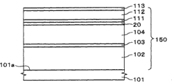
Fig. 1 and Fig. 2 are the generalized section of the optical element 100 of suitable embodiments of the present invention.In addition, Fig. 3 is the floor map of expression optical element 100 illustrated in figures 1 and 2.And Fig. 1 is the generalized section along the A-A line of Fig. 3, and Fig. 2 is the generalized section along the B-B line of Fig. 3.
The optical element 100 of present embodiment as shown in Figure 1, comprises surface-emitting type semiconductor laser 140, first insulating barrier 30, separator 20, photodetector 120 and second insulating barrier 40.
Below, surface-emitting type semiconductor laser 140, first insulating barrier 30, separator 20, photodetector 120 and second insulating barrier 40 and overall structure are described.
1-1. surface-emitting type semiconductor laser
Surface-emitting type semiconductor laser 140 is arranged on the Semiconductor substrate (being n type GaAs substrate in the present embodiment) 101.This surface-emitting type semiconductor laser 140 has vertical resonator.In addition, this surface-emitting type semiconductor laser 140 can comprise that the semiconductor of column is piled up body (hereinafter referred to as " cylindrical portion ") 130.
Surface-emitting type semiconductor laser 140, for example, by n type Al
0.9Ga
0.1As layer and n type Al
0.15Ga
0.8540 pairs of distributed reflection multilayer reflectors of As layer interaction cascading (below, be called " first reflector ") 102, by GaAs potential well layer and Al
0.3Ga
0.7The As barrier layer constitutes, and by comprising that potential well layer is to form with the active layer 103 of three layers of quantum potential well structure that constitutes and the 25 pairs of distributed reflection multilayer reflectors (below, be called " second reflector ") 104 lamination successively.And, the superiors 14 of second reflector 104, be the Al composition little be p type Al
0.15Ga
0.85As.
In this example, the Al composition of AlGaAs layer is the composition for the aluminium (Al) of gallium (Ga).The Al composition of AlGaAs layer is 0 to 1.That is, the AlGaAs layer comprises GaAs layer (the Al composition is 0) and AlAs layer (the Al composition is 1).
The composition and the number of plies that constitute each layer of first reflector 102, active layer 103 and second reflector 104 are not limited thereto.And the Al composition of the superiors 14 of second reflector 104 is preferably less than 0.3.For its reason, explanation below.
In surface-emitting type semiconductor laser 140, at mid portion,, be etched into round-shapedly from the upper surface 104a of second reflector 104 from second reflector, 104 to first reflectors 102, form columnar portion 130.In the present embodiment, though the flat shape of cylindrical portion 130 is circular, its shape can form shape arbitrarily.
The zone of approaching active layer 103 in constituting the layer of second reflector 104 forms the current blocking layer 105 that the oxidation from the side of AlGaAs layer obtained.This current blocking layer 105 forms ring-type.That is, this current blocking layer 105, the section shape the when face parallel with the surperficial 101a of as depicted in figs. 1 and 2 Semiconductor substrate 101 cuts off, the ring-type of the circle of the circular shape concentric of the flat shape of cylindrical portion 130.
In surface-emitting type semiconductor laser 140, be provided with first electrode 107 and second electrode 109.This first electrode 107 and second electrode 109 are used for drive surface emitting laser diode 140.
Particularly, as shown in Figure 1, first electrode 107 is arranged on the top 102a of first reflector 102.As shown in Figure 3, first electrode 107 has the flat shape of ring-type.That is, first electrode 107 mainly surrounds cylindrical portion 130.That is to say that cylindrical portion 130 is arranged on the inboard of first electrode 107.
In the present embodiment, only show first electrode 107 is arranged on situation on first reflector 102, still, also first electrode 107 can be arranged on the inside 101b of Semiconductor substrate 101.
1-2. first insulating barrier
In according to the optical element in the present embodiment 100, form first insulating barrier 30 that mainly surrounds cylindrical portion 130.First insulating barrier 30 is formed at the top of first reflector 102.And first insulating barrier 30 is formed at the below of the lead division 109b and the 109c of pad portion of second electrode 109 described later.And first insulating barrier 30 is formed at the below of second insulating barrier 40 described later.
1-3. separator
In the optical element 100 in the present embodiment, on surface-emitting type semiconductor laser 140, form separator 20.Separator 20 is arranged between surface-emitting type semiconductor laser 140 and the photodetector described later 120.Particularly, as depicted in figs. 1 and 2, separator 20 is arranged on second reflector 104.That is, separator 20 is arranged between second reflector 104 and first contact layer 111 described later.
The flat shape of separator 20 is circular.In illustrated example, the flat shape of separator 20 is identical with the flat shape of first contact layer 111.The flat shape of separator 20 can be bigger than the flat shape of first contact layer 111.For separator 20, in the manufacture method of optical element described later, describe in detail.
1-4. photodetector
In addition, photodetector 120 comprises first contact layer 111, light absorbing zone 112, second contact layer 113.First contact layer 111 is arranged on the separator 20; Light absorbing zone 112 is arranged on first contact layer 111; Second contact layer 113 is arranged on the light absorbing zone 112.The flat shape of first contact layer 111 is than the flat shape big (with reference to Fig. 1 and Fig. 2) of the light absorbing zone 112 and second contact layer 113.Second contact layer 113 and light absorbing zone 112 constitute the semiconductor of column and pile up body.
On optical detection part 120, be provided with third electrode 116 and the 4th electrode 110.This third electrode 116 and the 4th electrode 110 are used to drive photodetector 120.Particularly, as depicted in figs. 1 and 2, third electrode 116 covers first contact layer 111.The part of third electrode 116 is formed on the second above-mentioned electrode 109.That is, third electrode 116 is electrically connected with second electrode 109.As shown in Figure 3, third electrode 116 has the flat shape of ring-type.That is, third electrode 116 mainly surrounds first contact layer 111 and second insulating barrier 40.That is to say that first contact layer 111 and second insulating barrier 40 are arranged on the inboard of third electrode 116.
As shown in Figure 3, the 4th electrode 110 comprise the flat shape with ring-type connecting portion 110a, have the lead division 110b of the flat shape of linearity, the 110c of pad portion with circular flat shape.The 4th electrode 110 is electrically connected with second contact layer 113 in connecting portion 110a.The lead division 110b of the 4th electrode 110 makes connecting portion 110a be connected with the 110c of pad portion.The 110c of pad portion of the 4th electrode 110 can be used as electronic pads.The 4th electrode 110 is arranged on the upper surface (on second contact layer 113) of photodetector 120.The 4th electrode 110 is provided with peristome 114, by this part above peristome 114 exposed second contact layers 113.Should exposed face be laser-emitting face 108.Thereby,, just can appropriately set the shape and the size of exit facet 108 by the flat shape and the size of appropriate setting peristome 114.In the present embodiment, as shown in Figure 3, the exit facet 108 that illustrates is for circular.
In the optical element 100 of present embodiment, third electrode 116 can use the material identical with first electrode 107 to form, and the 4th electrode 110 then can use the material identical with second electrode 109 to form.
1-5. second insulating barrier
In the optical element 100 of present embodiment, form second insulating barrier 40 that mainly surrounds the light absorbing zone 112 and second contact layer 113.As shown in Figures 1 to 3, second insulating barrier 40 is formed at the top of first contact layer 111, second reflector 104 and first insulating barrier 30.And second insulating barrier 40 is formed at the below of the lead division 110b and the 110c of pad portion of the 4th electrode 110.
1-6. overall structure
In the optical element 100 of present embodiment, constitute the npnp structure by n type first reflector 102 of surface-emitting type semiconductor laser 140 and n type first contact layer 111 and p type second contact layer 113 integral body of p type second reflector 104 and photodetector 120.
More specifically, in photodetector 120, a part of absorbed layer 112 of the light that is produced by surface-emitting type semiconductor laser 140 is absorbed, and generates light stimulus by this absorbed light in light absorbing zone 112, and generation electronics and hole.By the electric field that applies from element-external, electronics is to third electrode 116 migrations, and the hole is then to 110 migrations of the 4th electrode.Its result in photodetector 120, generates electric current along the direction from first contact layer, 111 to second contact layers 113.
In addition, the output of the light of surface-emitting type semiconductor laser 140 depends primarily on the bias voltage that is applied on the surface-emitting type semiconductor laser 140.The light output of surface-emitting type semiconductor laser 140 can produce significantly because the life-span of the environment temperature of surface-emitting type semiconductor laser 140 and surface-emitting type semiconductor laser 140 is different and change.Therefore, in surface-emitting type semiconductor laser 140, need to keep predetermined light output.
In optical element 100 according to this form of implementation, the light output that produces by surface-emitting type semiconductor laser 140 by monitoring, adjust the current value that produces based on photodetector 120 and be applied to voltage on the surface-emitting type semiconductor laser 140, thereby be adjusted at value of current flowing in the surface-emitting type semiconductor laser 140.Therefore, can in surface-emitting type semiconductor laser 140, keep predetermined light output.Can utilize external electronic circuits (drive circuit: not shown) to implement FEEDBACK CONTROL, this FEEDBACK CONTROL is the light of surface-emitting type semiconductor laser 140 to be exported be fed back to the magnitude of voltage that is applied to surface-emitting type semiconductor laser 140.
2. the action of optical element
Below show the routine action of the optical element 100 of present embodiment.The driving method of following optical element 100 only is an example, can do all distortion under the prerequisite that does not exceed aim of the present invention.
At first, by first electrode 107 and second electrode 109 when the pin diode applies the voltage of positive direction, in the active layer 103 of surface-emitting type semiconductor laser 140, cause electronics and hole again in conjunction with and because of this again in conjunction with luminous.When the light that generate this moment comes and goes, cause stimulated emission between second reflector 104 and first reflector 102, thereby amplify light intensity.When the gain of light surpasses light loss, laser generation will take place, 104a penetrates laser above second reflector 104, incides separator 20.Afterwards, this laser incides first contact layer 111 of photodetector 120.
Secondly, in photodetector 120, incide the light of first contact layer 111, incide light absorbing zone 112 subsequently.The part of this incident light is absorbed at light absorbing zone 112, and the result generates light stimulus in light absorbing zone 112, and generates electronics and hole.In addition, by being applied to the electric field of element-external, electronics moves to third electrode 116, and then move to the 4th electrode 110 in the hole.Its result is at the electric current (photoelectric current) of photodetector 120 generations from first contact layer, 111 to second contact layers, 113 directions.By detecting this current value, can examine the light output of detection faces emitting laser diode 140.
3. the manufacture method of optical element
Below, the example around the manufacture method of the optical element 100 that is suitable for first execution mode of the present invention describes with reference to Fig. 4~Figure 13.Fig. 4~Figure 13 is the generalized section of a manufacture process of the optical element 100 shown in Fig. 1 to 3, separately corresponding to profile shown in Figure 1.
(1) at first, on the surperficial 101a of the Semiconductor substrate 101 that constitutes by n type GaAs,, form semiconductor multi layer film 150 as shown in Figure 4 while carry out epitaxially grown method by adjusting to form.Wherein, semiconductor multi layer film 150 for example can be by constituting with the lower part: n type Al
0.9Ga
0.1As layer and n type Al
0.15Ga
0.8540 couple, first reflector 102 that the As layer is alternately laminated; Comprise by GaAs potential well layer and Al
0.3Ga
0.7That the As barrier layer constitutes and by 3 layers of active layer 103 that constitutes the multi-quantum pit structure of potential well layer; By p type Al
0.9Ga
0.1As layer and p type Al
0.15Ga
0.85Second reflector 104 that 5 couple, the first district 104a that the As floor is alternately laminated and the 20 couples second district 104b constitute, first contact layer 111 that constitutes by n type GaAs, the light absorbing zone 112 that constitutes by the GaAs of impurity not and form by second contact layer 113 that p type GaAs constitutes.By these layers are layered on the Semiconductor substrate 101 according to the order of sequence, formed semiconductor multi layer film 150.And separator 20 also can be made of p type or n type AlGaAs layer.
Rate of etch when separator 20 can be to use second etchant described later, the rate of etch when using second etchant than the superiors 14 of second reflector 104 is big.Particularly, for example separator 20, can be made of the AlGaAs layer with Al composition bigger than the Al composition of the superiors 14 of second reflector 104.That is to say, when making 104 growths of second reflector, the superiors 14 of second reflector 104, the AlGaAs layer littler than the Al composition of separator 20 by the Al composition constitutes.More specifically, be preferably formed the superiors 14 and the separator 20 of second reflector 104 as described below, for example, the Al composition less than 0.3 of the superiors 14 of second reflector 104, the Al composition of separator 20 is greater than 0.3.
Rate of etch when separator 20 can be to use first etchant described later, the rate of etch when using first etchant than first contact layer 111 is little.Particularly, for example separator 20, can be made of the AlGaAs layer with Al composition bigger than the Al composition of first contact layer 111.That is to say, when making 111 growths of first contact layer, first contact layer 111, the AlGaAs layer (comprise GaAs) littler than the Al composition of separator 20 by the Al composition constitutes.More specifically, be preferably formed first contact layer 111 and separator 20 as described below, for example, the Al composition less than 0.3 of first contact layer 111, the Al composition of separator 20 is greater than 0.3.
When making 104 growths of second reflector, near the one deck at least that forms active layer 103 carries out oxidation afterwards, and formation will become the layer (with reference to Fig. 9) of current blocking layer 105.Particularly, becoming the layer of current blocking layer 105, is the Al composition AlGaAs layer (comprise AlAs) bigger than the Al composition of separator 20.That is to say that separator 20 can be that the Al composition is than the little AlGaAs layer of layer that becomes current blocking layer 105.Therefore, in the oxidation step of formation current blocking layer 105 described later (with reference to Fig. 9), separator 20 can be not oxidized.Particularly, for example, the Al composition that preferably makes the layer that becomes current blocking layer 105 makes the Al composition less than 0.95 of separator 20 more than or equal to 0.95.
When the design wavelength of surface-emitting type semiconductor laser 140 (seeing figures.1.and.2) was λ, the blooming of separator 20 for example can be the odd-multiple of λ/4.
The summation of the optical film thickness of first contact layer 111, light absorbing zone 112 and second contact layer 113, that is, the optical film thickness of overall optical detecting element 120 (seeing figures.1.and.2) for example can be the odd-multiple of λ/4.Its result, overall optical detecting element 120 can be used as the distributed reflection reflector and works.That is, above the active layer 103 of surface-emitting type semiconductor laser 140, overall optical detecting element 120 can be used as the distributed reflection reflector and works.Therefore, characteristic that can influence surface emitting laser diode 140, photodetector 120 can be used as the distributed reflection reflector and works.
Preferably in the back operation when forming second electrode 109, improve second reflector 104 at least with second electrode, 109 coupling parts near carrier density, it is obtained easily with the ohmic properties of second electrode 109 contacts.Equally, be in first contact layer 111 at least with third electrode 116 coupling parts near, improve carrier density contact so that obtain easily with the ohmic properties of third electrode 116.
Temperature when carrying out epitaxial growth suitably determines according to the kind of growing method and raw material and Semiconductor substrate 101 or kind, thickness and the carrier density of formation semiconductor multi layer film 150, generally is preferably 450 ℃ to 800 ℃.In addition, also the same with temperature, the required time when suitably determining epitaxial growth.Epitaxial growth method can adopt organic metal vapor growth method (MOVPE:Metal-Organic Vapor Phase Epitaxy) and MBE (molecular beam epitaxy: method or LPE (liquid phase epitaxial method: method Liquid Phase Epitaxy) Molecular Beam Epitaxy).
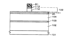
(2) then, second contact layer 113 and light absorbing zone 112 formed the pattern (with reference to Fig. 5) of reservation shapes.
At first, on semiconductor multi layer film 150, apply photoresist (not having diagram) afterwards, adopt photoetching process on this photoresist layer, to form pattern, form the resist layer R1 of predetermined pattern.
Then, as mask, for example, adopt resist layer R1 dry ecthing method that second contact layer 113 and light absorbing zone 112 are carried out etching.The light absorbing zone 112 that forms second contact layer 113 thus and have second contact layer, 113 same level shapes.Second contact layer 113 and light absorbing zone 112 constitute the semiconductor of column and pile up body.Afterwards, remove resist layer R1.
(3) then, first contact layer 111 is formed the pattern (with reference to Fig. 6) of regulation shape.Specifically, at first on first contact layer 111, apply resist (not having diagram), adopt photoetching process to make on this resist layer then and form pattern, thus the resist layer R2 of formation compulsory figure.
Secondly, with resist layer R2 as mask, with first etchant etching, first contact layer 111.At this moment, configuration isolation layer 20 below first contact layer 111, because separator 20 works as etchant resistive layer, separator 20 exposes the etching of first contact layer 111, therefore, accurately and easily.Below, carry out specific description.
As mentioned above, separator 20 can be, and is little with the rate of etch of first contact layer 111 of first etchant with the rate of etch ratio of first etchant.That is, at first, the big rate of etch of first contact layer, 111 usefulness with separator 20 etchings till exposing.So separator 20 exposes.
The rate of etch of separator 20 is littler than the rate of etch of first contact layer 111.In other words, separator 20 to the first contact layers 111 are difficult for etched.Thereby, when separator 20 exposes,, therefore, stop etching easily at this moment owing to be difficult for taking place with the etching of first etchant.That is, exposing in 20, can be accurately and stop 111 etchings of first contact layer easily.
More specifically, for example, separator 20 can be made of the Al composition AlGaAs layer bigger than the Al composition of first contact layer 111.And, can select first etchant, its rate of etch in the big AlGaAs layer of Al composition is little, and the rate of etch in the little AlGaAs layer of Al composition is big.That is, select first etchant, its AlGaAs layer that optionally etching Al composition is little.Therefore, can use the rate of etch of separator 20 of first etchant less than rate of etch with first contact layer 111 of first etchant.
As mentioned above, the Al composition of separator 20 is preferably more than 0.3, and the Al composition less than 0.3 of first contact layer 111.At this moment, can use the mixed solution of ammonia and hydrogen peroxide and water as first etchant.For example, the mixed proportion of ammonia and hydrogen peroxide and water can be 1: 10: 150, and still, mixed proportion is not particularly limited, and can suitably select.
Therefore, shown in Figure 6, form photodetector 120.Photodetector 120 comprises second contact layer 113, light absorbing zone 112 and first contact layer 111.And the flat shape of first contact layer 111 is bigger than the flat shape of second contact layer 113 and light absorbing zone 112.
In above-mentioned steps, illustrated behind second contact layer 113 and light absorbing zone 112 formation patterns, form the situation of pattern at first contact layer 111, but also can after first contact layer 111 forms pattern, form pattern at second contact layer 113 and light absorbing zone 112.
(4) secondly, form the pattern (with reference to Fig. 7) of reservation shape at separator 20.Particularly, with above-mentioned resist layer R2 as mask, with the second etchant etching separator 20.At this moment, below separator 20, be provided with the superiors 14 of second reflector 104, because the superiors 14 of second reflector 104 work as etchant resistive layer, when the superiors 14 of second reflector 104 exposed, separator 20 correctly and easily stopped etching.Below, be described in detail.
As mentioned above, separator 20 can be, and is big with the rate of etch of the superiors 14 of second reflector 104 of second etchant with the rate of etch ratio of second etchant.That is, at first, the big rate of etch of the superiors' 14 usefulness of second reflector 104 with separator 20 etchings till exposing.So the superiors 14 of second reflector 104 expose.
The rate of etch of the superiors 14 of second reflector 104 is littler than the rate of etch of separator 20.In other words, the superiors 14 of second reflector 104 are difficult for etched than separator 20.Thereby, when the superiors 14 of second reflector 104 expose,, therefore, stop etching easily at this moment owing to be difficult for taking place with the etching of second etchant.That is, in the superiors 14 of exposing second reflector 104, can be accurately and stop the etching of separator 20 easily.
More specifically, for example, separator 20 can be made of the Al composition AlGaAs layer bigger than the Al composition of the superiors 14 of second reflector 104.And, can select second etchant, its rate of etch in the big AlGaAs layer of Al composition is big, and the rate of etch in the little AlGaAs layer of Al composition is little.That is, select second etchant, its AlGaAs layer that optionally etching Al composition is big.Therefore, can use the rate of etch of separator 20 of second etchant greater than rate of etch with the superiors 14 of second reflector 104 of second etchant.
As mentioned above, the Al composition of separator 20 is preferably more than 0.3, and the A l composition less than 0.3 of the superiors 14 of second reflector 104.At this moment, can use fluorinated, acid as second etchant.This fluorinated, acid concentration for example can be 0.1%, but is not particularly limited, and can suitably select.
Therefore, shown in Figure 7, form the separator 20 that is formed pattern.Thereafter, resist layer R2 is removed.As shown in the figure, the flat shape of separator 20 is identical with the flat shape of first contact layer 111, but the flat shape of separator 20 can be bigger than the flat shape of first contact layer 111.Particularly, adopt other resist layers bigger, replace above-mentioned resist layer R2 when separator 20 forms pattern, form pattern at separator 20 than the flat shape of resist layer R2.
(5) secondly, according to forming pattern, form the surface-emitting type semiconductor laser 140 (with reference to Fig. 8) that comprises cylindrical portion 130.Particularly, at first, behind painting erosion resistant agent on second reflector 104 (not having diagram), form pattern at this resist layer, form the resist layer R3 of predetermined pattern by photoetching process.Secondly, with resist layer R3 as mask, for example, by the part of dry ecthing method etching second reflector 104, active layer 103 and first reflector 102.Therefore, as shown in Figure 8, form cylindrical portion 130.
According to above step, on Semiconductor substrate 101, form the vertical resonator (surface-emitting type semiconductor laser 140) that comprises cylindrical portion 130.That is, form the laminated body of surface-emitting type semiconductor laser 140, separator 20 and photodetector 120.Then, resist layer R3 is removed.
In the present embodiment, as mentioned above, be illustrated, but also can form photodetector 120 and separators 20 forming stylolitic part 130 backs at first forming the situation that photodetector 120 and separator 20 form stylolitic part 130 then.
(6) then, for example, the Semiconductor substrate 101 that adopts above-mentioned technology to form stylolitic part 130 is put in 400 ℃ the steam dielectric gas, from the side the big layer of Al composition that is provided with in second reflector 104 carried out oxidation, form narrow current sheet 105 (with reference to Fig. 9).As mentioned above, in this step, separator 20 can be not oxidized.
Oxygenation efficiency depend on furnace temperature, steam quantity delivered, answer the Al of oxide layer to form and film thickness.In the surface-emitting type semiconductor laser with the current blocking layer that forms because of oxidation, when driving, electric current only flows not forming the part of current blocking layer (not oxidized portion).Thereby, forming by oxidation in the step of current blocking layer, by the scope of control formation current blocking layer 105, can Control current density.
In addition, preferably adjust the diameter of current blocking layer 105, making can incident first contact layer 111 from most of light of surface-emitting type semiconductor laser 140 emissions.
(7) secondly, as shown in figure 10, on first reflector 102, around cylindrical portion 130, form first insulating barrier 30.First insulating barrier 30 can use the material of comparing easy thick filmization with second insulating barrier 40.For example, first insulating barrier 30 can adopt the energy according to heat or light etc. obtains hardenable fluent material (for example precursor of uv-hardening resin and thermmohardening type resin) by induration material.As uv-hardening resin, for example, it is resin that UV cured type propylene resin and epoxy are arranged.And as thermmohardening type resin, it is resin that thermmohardening type polyimides is arranged.In addition, for example, first insulating barrier 30 can adopt a plurality of above-mentioned materials as stack membrane.
At this, as the material that forms first insulating barrier 30, adopting polyimides is resin precursor.At first, for example, use the spin rubbing method that precursor (polyimides is a resin precursor) is coated on the Semiconductor substrate 101, form precursor layer.And,,, also can use known technologies such as infusion process, spraying process, ink-jet method except the spin rubbing method as the formation method of precursor layer.
Then, with this Semiconductor substrate 101, for example use electric furnace etc. to add the heat abstraction solvent after, put into the stove about 350 ℃, by with the precursor layer imidizate, form the almost completely polyimides resin of sclerosis.Then, as shown in figure 10, form pattern at the polyimides resin, form first insulating barrier 30 by adopting well-known lithography technology.The etching method that uses during as the formation pattern can adopt dry ecthing method etc.Dry ecthing method for example can carry out etching by plasmas such as oxygen or argons.
And in the formation method of the first above-mentioned insulating barrier 30, cured polyimide is after the precursor layer of resin, carries out pattern and forms, and still, also can carry out pattern and form before cured polyimide be the precursor layer of resin.Engraving method as using when forming pattern can use wet etch method.Wet etching for example can utilize aqueous slkali or organic solution etc. to carry out.
(8) secondly, as shown in figure 11, on first contact layer 111, around second cylindrical portion 132, form second insulating barrier 40.Second insulating barrier 40 can adopt than first insulating barrier, the 30 easier materials that carry out retrofit.The film thickness of second insulating barrier 40 for example is 0.1~0.5 μ m, but is not limited thereto, can be than the thin film thickness of first insulating barrier 30.For example, second insulating barrier 40 can adopt dielectric film or its stack membrane of mineral-type such as silicon dioxide film and silicon nitride film.Below, specify the formation method of second insulating barrier 40.
At first, on the Semiconductor substrate 101 that forms surface-emitting type semiconductor laser 140 and photodetector 120, form insulating barrier (not shown) comprehensively.This insulating barrier is by formation such as plasma CVD methods.In addition, this insulating barrier is formed by adopting well-known photoetching process to carry out pattern, form second insulating barrier 40.As mentioned above, the pattern of second insulating barrier 40 forms and can carry out the processing meticulousr than first insulating barrier 30.The etching method that uses during as this pattern of formation can use dry ecthing method or wet etch method etc.Dry ecthing method is to be undertaken by containing fluorine-based plasma.Wet etching is to be undertaken by fluoric acid.
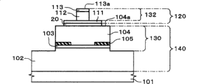
(9) then, 104a on second reflector 104 forms second electrode 109; And on photodetector 120 (second contact layer 113 above 113a), form the 4th electrode 110 (with reference to Figure 12).
At first, before forming second electrode 109 and the 4th electrode 110, as required, can utilize plasma processing method that the top 104a of second reflector 104 and the 113a of second contact layer, 113 upper surfaces are cleaned.Thereby formation has the more element of stability characteristic (quality).
Secondly, by for example vacuum vapour deposition, form for example stacked film (not shown) of platinum (Pt), titanium (Ti) and gold (Au).Then, adopt and peel off method (lift-off), the stacked film outside the assigned position is removed, form second electrode 109 and the 4th electrode 110.At this moment, 113a on second contact layer 113 forms the part that is not formed described stacked film.This part is an opening portion 114, by opening portion 114, exposes the top 113a of a part of second contact layer 113.The exit facet 108 that this face that exposes is a laser.
As mentioned above, second electrode 109 contains platinum (Pt) at least.Second electrode 109 can use the alloy of gold (Au) and zinc (Zn), but second electrode 109 preferably contains platinum.Below, its reason is described.
In addition, in above-mentioned steps, replace peeling off method and can adopt dry ecthing method or wet etch method.In addition, in above-mentioned steps, replace vacuum vapour deposition can adopt gunite.In addition, in above-mentioned steps, second electrode 109 and the 4th electrode 110 form pattern simultaneously, but second electrode 109 and the 4th electrode 110 can each self-forming patterns.
(10) secondly, adopt and use the same method, for example, on the stack membrane of the alloy of gold (Au) and germanium (Ge) and gold (Au), form pattern, on first reflector 102 of surface-emitting type semiconductor laser 140, form first electrode 107, on first contact layer 111 of photodetector 120, form third electrode 116 (with reference to Figure 13).First electrode 107 and third electrode 116 can form pattern simultaneously, or first electrode 107 and third electrode 116, but each self-forming pattern.
(11) secondly, anneal.Temperature according to electrode material decision annealing.For the electrode material that in this example, adopts, about 400 ℃, carry out usually.By above step, form first to fourth electrode 107,109,110,116.
According to above step,, obtain the optical element 100 of this example as Fig. 1~shown in Figure 3.
4. act on and effect
According to the optical element 100 of this example, around first cylindrical portion 130, form first insulating barrier 30, around second cylindrical portion 132, form second insulating barrier 40.That is, according to the optical element 100 of this example, can be at first insulating barrier and second insulating barrier of each predetermined zone (perpendicular to the zone of described substrate 101) configuration expectation.Particularly, can form first insulating barrier 30 in the zone of first cylindrical portion 130 with surface-emitting type semiconductor laser 140.And, can form second insulating barrier 40 in the zone of second cylindrical portion 132 with photodetector 120.
According to the optical element 100 of this example, around first cylindrical portion 130, form first insulating barrier 30.First insulating barrier 30 is compared with second insulating barrier 40, easily thick filmization.By forming the first thick insulating barrier 30, can reduce the parasitic capacitance of surface-emitting type semiconductor laser 140.Its result can realize the high-speed driving of surface-emitting type semiconductor laser 140.
According to the optical element 100 of this example, around second cylindrical portion 132, form second insulating barrier 40.Second insulating barrier 40 is compared with first insulating barrier 30 and is carried out retrofit easily.By second insulating barrier 40 is carried out retrofit, the electrode that has meticulous and complicated structure in photodetector 120 is insulated.
According to the manufacture method of the optical element 100 of this example, form the step of first insulating barrier 30 respectively and form the step of second insulating barrier 40.Therefore, can form and have first insulating barrier 30 of obtaining above-mentioned effect and effect and the optical element 100 of second insulating barrier 40.
Manufacture method according to the optical element 100 of this example, in the step of etching first contact layer 111, owing to below first contact layer 111, have separator 20, this separator 20 has the function as etchant resistive layer, therefore can high accuracy, correct, be easy to carry out the etching of first contact layer 111.
Lack according to the Al composition of optical element 100, the first contact layers 111 of this example Al composition than separator 20.Thereby,, therefore obtain first contact layer 111 easily and contact with the ohmic properties of third electrode 116 owing to can make the Al composition of first contact layer 111 few.As mentioned above, the Al composition of first contact layer 111 is preferably less than 0.3.Because the Al composition less than 0.3 of first contact layer 111 obtains good first contact layer 111 and contacts with the ohmic properties of third electrode 116.
Lack according to the Al composition of the superiors 14 of optical element 100, the second reflectors 104 of this example Al composition than separator 20.Thereby owing to the Al composition of the superiors 14 that can make second reflector 104 is few, the superiors 14 that therefore obtain second reflector 104 easily contact with the ohmic properties of second electrode 109.As mentioned above, the Al composition of the superiors 14 of second reflector 104 is preferably less than 0.3.Because the Al composition less than 0.3 of the superiors 14 of second reflector 104, the superiors 14 that obtain good second reflector 104 contact with the ohmic properties of second electrode 109.
According to the optical element 100 of this example, the Al composition of separator 20 is bigger than the Al composition of the superiors 14 of second reflector 104, and is bigger than the Al composition of first contact layer 111.In other words, in the superiors 14 of second reflector 104, form the big separator 20 of Al composition that has than the superiors 14 of second reflector 104.And on separator 20, formation has Al composition first contact layer 111 littler than the Al composition of this separator 20.As mentioned above, by the different layer of stacked Al composition, this stack membrane (the superiors 14 of second reflector 104, separator 20, and first contact layer 111) can be used as reflector.That is to say, under the impregnable situation of the characteristic of surface-emitting type semiconductor laser 140, adopt the separator 20 and first contact layer 111, improve the Design of device degree of freedom as reflector.
According to the optical element 100 of this example, become the odd-multiple of λ/4 by the blooming that makes separator 20, separator 20 has the function as the distributed reflection reflector.That is to say that second reflector 104 and separator 20 in surface-emitting type semiconductor laser 140 above active layer 103, have the function as the distributed reflection reflector.Thereby, the characteristic of influence surface emitting laser diode 140 not, separator 20 has the function as the distributed reflection reflector.
According to the optical element 100 of this example, form not oxidized separator 20.That is to say, in optical element 100 and manufacture method thereof, in the oxidation step that is used to form current blocking layer 105, can make separator 20 not oxidized according to this example.Because separator 20 is not oxidized, can prevent that the intensity that oxidation causes is low.In addition, because separator 20 is not oxidized, can prevent that the refractive index that oxidation causes is low inferior.Its result when separator 20 works as reflector, can prevent from reflectivity etc. is brought harmful effect.
According to the optical element 100 of this example, to use the part of the light output of photodetector 120 control surface emitting laser diodes 140, and feed back to drive circuit, the output change that revisal temperature etc. causes can obtain stable light output.
More than explanation is preferred example of the present invention, but the present invention is not limited to this, can take various forms.For example, as shown in figure 14, second electrode 109 and third electrode 116 can connect by connection electrode 117.Particularly, connection electrode 117 is connected above second electrode 109, and, be connected the top and side of third electrode 116.As connection electrode 117, can adopt the material of gold etc., but be not limited to this, can adopt well-known metal, alloy or its stack membrane.And Figure 14 is the profile of expression according to Fig. 1.
And, in above-mentioned example, form third electrode 116 covering the part above second electrode 109, but as shown in figure 15, also can form second electrode 109 to cover a top part and the side of third electrode 116.And Figure 15 is the profile of expression according to Fig. 1.
In addition, in above-mentioned example,, can not break away from aim of the present invention even intercourse the p type n type of each semiconductor layer yet.At this, p type first reflector 102 of surface-emitting type semiconductor laser 140 and n type second reflector 104, and p type first contact layer 111 of photodetector 120 and n type second contact layer 113 constitute pnpn structure as a whole.And, at this moment, can intercourse the material of second electrode 109 and third electrode 116.That is to say, particularly, with second electrode 109 that n type second reflector 104 is connected, can adopt the alloy of gold (Au) and germanium (Ge) and the stack membrane of gold (Au) etc., third electrode 116 with p type first contact layer 111 is connected can adopt the material of platiniferous (Pt) etc.
In addition, for example, in surface-emitting type semiconductor laser 140 or photodetector 120 either party by p type and the n type of intercoursing each layer, can become npn structure or pnp structure with surface-emitting type semiconductor laser 140 and photodetector 120 integral body.And at this moment, second cylindrical portion 132 can comprise first contact layer 111.
In addition, in above-mentioned example, the situation that forms separator 20 between second reflector 104 and first contact layer 111 has been described, for example, between second reflector 104 and first contact layer 111, can formed separator 20.
Symbol description
14 the superiors; 20 separation layers; 30 first insulating barriers; 40 second insulating barriers; 100 light Element; 101 substrates; 102 first reflectors; 103 active layers; 104 second reflectors; 105 current blocking layers; 107 first electrodes; 108 exit facets; 109 second electrodes; 110 The 4th electrode; 111 first contact layers; 112 light absorbing zones; 113 second contact layers; 114 Peristome; 116 third electrodes; 117 connecting electrodes; 120 photodetectors; 130 One columnar part; 132 second columnar part; 140 surface-emitting type semiconductor lasers.
Claims (10)
1. optical element comprises:
Surface-emitting type semiconductor laser, it is included in first reflector, active layer and second reflector of the top of substrate from described substrate side configuration;
Photodetector, it is included in first contact layer, light absorbing zone and second contact layer of the top of described surface-emitting type semiconductor laser from described surface-emitting type semiconductor laser side configuration;
First insulating barrier, it is formed at the top of described substrate;
Second insulating barrier, it is formed at the top of described surface-emitting type semiconductor laser;
Described first insulating barrier covers the side of first cylindrical portion but does not cover the end face of first cylindrical portion, and described first cylindrical portion comprises the part of described second reflector at least,
Described second insulating barrier covers the side of second cylindrical portion, and described second cylindrical portion comprises the part of described second contact layer at least,
The diameter of described second cylindrical portion is littler than the diameter of described first cylindrical portion,
The thickness of described first insulating barrier of the Film Thickness Ratio of described second insulating barrier is thin.
2. optical element according to claim 1, wherein, described first insulating barrier is made of resin, and described second insulating barrier is made of the dielectric of mineral-type.
3. optical element according to claim 2, wherein, described resin is that resin, propylene resin, epoxy are resin or fluorine resin for poly-imines, the dielectric of described mineral-type is silicon nitride or silicon dioxide.
4. the manufacture method of an optical element, described optical element comprises surface-emitting type semiconductor laser and photodetector, wherein, described method comprises the steps:
The step of stacked semiconductor layer above substrate, described semiconductor layer are used for forming at least first reflector, active layer, second reflector, first contact layer, light absorbing zone and second contact layer;
Form the step of first cylindrical portion by the described semiconductor layer of etching, described first cylindrical portion comprises the part of described second reflector at least;
Form the step of second cylindrical portion by the described semiconductor layer of etching, described second cylindrical portion comprises the part of described second contact layer at least;
Form the step of first insulating barrier with the side that covers described first cylindrical portion;
Form the step of second insulating barrier with the side that covers described second cylindrical portion, wherein,
The diameter of described second cylindrical portion is littler than the diameter of described first cylindrical portion,
The thickness of described first insulating barrier of the Film Thickness Ratio of described second insulating barrier is thin.
5. the manufacture method of optical element according to claim 4, wherein, the step that forms described first insulating barrier comprises the steps:
Form the step of precursor layer, described precursor layer covers the side of described first cylindrical portion at least;
Step in described precursor layer pattern-making;
The harden step of described precursor layer.
6. the manufacture method of optical element according to claim 5, wherein, with dry ecthing method or wet etch method in described precursor layer pattern-making.
7. according to the manufacture method of each described optical element in the claim 4 to 6, wherein,
The step that forms described second insulating barrier comprises the steps:
Form the step of insulating barrier with the side that covers described second cylindrical portion at least;
Step in described insulating barrier pattern-making.
8. the manufacture method of optical element according to claim 7, wherein, described second insulating barrier forms by plasma CVD method.
9. the manufacture method of optical element according to claim 7, wherein, with dry ecthing method or wet etch method in described first insulating barrier or the second insulating barrier pattern-making.
10. the manufacture method of optical element according to claim 8, wherein, with dry ecthing method or wet etch method in described first insulating barrier or the second insulating barrier pattern-making.
Applications Claiming Priority (2)
| Application Number | Priority Date | Filing Date | Title |
|---|---|---|---|
| JP2004003057 | 2004-01-08 | ||
| JP2004003057A JP3729271B2 (en) | 2004-01-08 | 2004-01-08 | Optical device and manufacturing method thereof |
Publications (2)
| Publication Number | Publication Date |
|---|---|
| CN1638215A CN1638215A (en) | 2005-07-13 |
| CN100438239C true CN100438239C (en) | 2008-11-26 |
Family
ID=34587705
Family Applications (1)
| Application Number | Title | Priority Date | Filing Date |
|---|---|---|---|
| CNB2004100987965A Expired - Fee Related CN100438239C (en) | 2004-01-08 | 2004-12-14 | Optical element, and its manufacturing method |
Country Status (5)
| Country | Link |
|---|---|
| US (1) | US7312508B2 (en) |
| EP (1) | EP1553667A3 (en) |
| JP (1) | JP3729271B2 (en) |
| KR (1) | KR100658996B1 (en) |
| CN (1) | CN100438239C (en) |
Families Citing this family (6)
| Publication number | Priority date | Publication date | Assignee | Title |
|---|---|---|---|---|
| JP4720637B2 (en) * | 2005-09-07 | 2011-07-13 | セイコーエプソン株式会社 | Optical element and manufacturing method thereof |
| JP2007103768A (en) * | 2005-10-06 | 2007-04-19 | Seiko Epson Corp | Optical semiconductor element and its fabrication process |
| US20070081568A1 (en) * | 2005-10-06 | 2007-04-12 | Seiko Epson Corporation | Optical semiconductor element and method for manufacturing the same |
| JP4269180B2 (en) | 2006-07-14 | 2009-05-27 | セイコーエプソン株式会社 | Manufacturing method of optical element |
| JP5321886B2 (en) * | 2009-02-06 | 2013-10-23 | ソニー株式会社 | Semiconductor element |
| JP2011096787A (en) * | 2009-10-28 | 2011-05-12 | Sony Corp | Semiconductor light emitting device |
Citations (4)
| Publication number | Priority date | Publication date | Assignee | Title |
|---|---|---|---|---|
| US5742630A (en) * | 1996-07-01 | 1998-04-21 | Motorola, Inc. | VCSEL with integrated pin diode |
| WO2001073856A2 (en) * | 2000-03-27 | 2001-10-04 | Aegis Semiconductor | A semitransparent optical detector on a flexible substrate and method of making |
| EP1341278A1 (en) * | 2002-03-01 | 2003-09-03 | Seiko Epson Corporation | Surface-emitting semiconductor light-emitting device and method of manufacturing the same, optical module, and light-transmission device |
| US6670599B2 (en) * | 2000-03-27 | 2003-12-30 | Aegis Semiconductor, Inc. | Semitransparent optical detector on a flexible substrate and method of making |
Family Cites Families (12)
| Publication number | Priority date | Publication date | Assignee | Title |
|---|---|---|---|---|
| JP3123026B2 (en) | 1992-08-24 | 2001-01-09 | 日本電信電話株式会社 | Si substrate top emission laser |
| US5606572A (en) * | 1994-03-24 | 1997-02-25 | Vixel Corporation | Integration of laser with photodiode for feedback control |
| MY120887A (en) * | 1995-06-08 | 2005-12-30 | Sony Corp | Rotation position detecting device and motor device. |
| US5757837A (en) * | 1996-10-16 | 1998-05-26 | The Regents Of The University Of California | Intracavity quantum well photodetector integrated within a vertical-cavity surface-emitting laser and method of operating same |
| KR100234339B1 (en) | 1996-10-28 | 1999-12-15 | 윤종용 | Surface emitting laser with integrated photodetector for power stabilization |
| KR100234340B1 (en) * | 1996-10-29 | 1999-12-15 | 윤종용 | Surface emitting laser with integrated photodetector for power stabilization |
| DE19807783A1 (en) * | 1998-02-18 | 1999-09-02 | Siemens Ag | Component with a light transmitter and a light receiver |
| KR100317576B1 (en) * | 1999-11-08 | 2001-12-24 | 윤덕용 | Surface emitting laser with a monolithically integrated monitor photdetector |
| JP4217855B2 (en) | 2000-05-08 | 2009-02-04 | 日本電気株式会社 | Semiconductor photo detector |
| JP4029271B2 (en) | 2001-03-09 | 2008-01-09 | セイコーエプソン株式会社 | Manufacturing method of surface light emitting element |
| JP4058633B2 (en) * | 2003-07-10 | 2008-03-12 | セイコーエプソン株式会社 | Surface-emitting light emitting device, optical module, optical transmission device |
| JP3738849B2 (en) * | 2003-08-07 | 2006-01-25 | セイコーエプソン株式会社 | Surface emitting semiconductor laser, optical module, and optical transmission device |
-
2004
- 2004-01-08 JP JP2004003057A patent/JP3729271B2/en not_active Expired - Fee Related
- 2004-12-08 KR KR1020040102731A patent/KR100658996B1/en not_active IP Right Cessation
- 2004-12-14 CN CNB2004100987965A patent/CN100438239C/en not_active Expired - Fee Related
-
2005
- 2005-01-04 EP EP05000047A patent/EP1553667A3/en not_active Withdrawn
- 2005-01-10 US US11/030,906 patent/US7312508B2/en not_active Expired - Fee Related
Patent Citations (4)
| Publication number | Priority date | Publication date | Assignee | Title |
|---|---|---|---|---|
| US5742630A (en) * | 1996-07-01 | 1998-04-21 | Motorola, Inc. | VCSEL with integrated pin diode |
| WO2001073856A2 (en) * | 2000-03-27 | 2001-10-04 | Aegis Semiconductor | A semitransparent optical detector on a flexible substrate and method of making |
| US6670599B2 (en) * | 2000-03-27 | 2003-12-30 | Aegis Semiconductor, Inc. | Semitransparent optical detector on a flexible substrate and method of making |
| EP1341278A1 (en) * | 2002-03-01 | 2003-09-03 | Seiko Epson Corporation | Surface-emitting semiconductor light-emitting device and method of manufacturing the same, optical module, and light-transmission device |
Also Published As
| Publication number | Publication date |
|---|---|
| JP2005197514A (en) | 2005-07-21 |
| KR100658996B1 (en) | 2006-12-21 |
| JP3729271B2 (en) | 2005-12-21 |
| EP1553667A2 (en) | 2005-07-13 |
| US20050161687A1 (en) | 2005-07-28 |
| KR20050073521A (en) | 2005-07-14 |
| CN1638215A (en) | 2005-07-13 |
| EP1553667A3 (en) | 2005-12-07 |
| US7312508B2 (en) | 2007-12-25 |
Similar Documents
| Publication | Publication Date | Title |
|---|---|---|
| US6222866B1 (en) | Surface emitting semiconductor laser, its producing method and surface emitting semiconductor laser array | |
| US6678307B2 (en) | Semiconductor surface light-emitting device | |
| JP3540042B2 (en) | Manufacturing method of semiconductor device | |
| US6201825B1 (en) | Surface emitting semiconductor laser device and process for producing the same | |
| CN100448124C (en) | Optical element, and its manufacturing method | |
| JPH11103129A (en) | Vertical cavity face light-emitting laser, and its manufacture | |
| JP2006032964A (en) | Vcsel equipped with air gap and protection coating layer | |
| TW200816586A (en) | Semiconductor device, and manufacturing method of the same | |
| US20050180481A1 (en) | Surface-emitting semiconductor laser and method of manufacturing the same | |
| US7312508B2 (en) | Optical element, and its manufacturing method | |
| Chua et al. | Planar laterally oxidized vertical-cavity lasers for low-threshold high-density top-surface-emitting arrays | |
| US20010050935A1 (en) | Surface emitting semiconductor laser device | |
| CN112152073A (en) | Surface emitting laser | |
| CN112152069A (en) | Surface emitting laser and method for manufacturing the same | |
| US20020197756A1 (en) | Surface-emitting semiconductor laser device and method for fabricating the same, and surface-emitting semiconductor laser array employing the laser device | |
| JP2006351921A (en) | Optical element | |
| KR101013422B1 (en) | Plane emission type semiconductor laser device and method of manufacturing the same | |
| US20070054437A1 (en) | Optical element and its manufacturing method | |
| CN112290376A (en) | Surface emitting laser and method of manufacturing the same | |
| US7643531B2 (en) | Optical semiconductor element including photodetecting element with comb-tooth structure | |
| WO1998048492A1 (en) | Electronic devices formed from pre-patterned structures that are bonded | |
| JPH10209565A (en) | Lateral current-injection type surface light-emitting semiconductor laser device, its manufacture, and semiconductor laser array | |
| JPH06350132A (en) | Semiconductor luminous element array | |
| US20040125841A1 (en) | Surface-emitting semiconductor laser device | |
| JP2006339486A (en) | Photo cell and its manufacturing method |
Legal Events
| Date | Code | Title | Description |
|---|---|---|---|
| C06 | Publication | ||
| PB01 | Publication | ||
| C10 | Entry into substantive examination | ||
| SE01 | Entry into force of request for substantive examination | ||
| C14 | Grant of patent or utility model | ||
| GR01 | Patent grant | ||
| CF01 | Termination of patent right due to non-payment of annual fee | ||
| CF01 | Termination of patent right due to non-payment of annual fee |
Granted publication date: 20081126 Termination date: 20181214 |