CN100474421C - Memory medium based on current distribution - Google Patents
Memory medium based on current distribution Download PDFInfo
- Publication number
- CN100474421C CN100474421C CNB021499020A CN02149902A CN100474421C CN 100474421 C CN100474421 C CN 100474421C CN B021499020 A CNB021499020 A CN B021499020A CN 02149902 A CN02149902 A CN 02149902A CN 100474421 C CN100474421 C CN 100474421C
- Authority
- CN
- China
- Prior art keywords
- conductor layer
- data storage
- energy
- layer
- medium
- Prior art date
- Legal status (The legal status is an assumption and is not a legal conclusion. Google has not performed a legal analysis and makes no representation as to the accuracy of the status listed.)
- Expired - Fee Related
Links
Images


Classifications
-
- G—PHYSICS
- G11—INFORMATION STORAGE
- G11B—INFORMATION STORAGE BASED ON RELATIVE MOVEMENT BETWEEN RECORD CARRIER AND TRANSDUCER
- G11B11/00—Recording on or reproducing from the same record carrier wherein for these two operations the methods are covered by different main groups of groups G11B3/00 - G11B7/00 or by different subgroups of group G11B9/00; Record carriers therefor
- G11B11/08—Recording on or reproducing from the same record carrier wherein for these two operations the methods are covered by different main groups of groups G11B3/00 - G11B7/00 or by different subgroups of group G11B9/00; Record carriers therefor using recording by electric charge or by variation of electric resistance or capacitance
-
- G—PHYSICS
- G11—INFORMATION STORAGE
- G11B—INFORMATION STORAGE BASED ON RELATIVE MOVEMENT BETWEEN RECORD CARRIER AND TRANSDUCER
- G11B11/00—Recording on or reproducing from the same record carrier wherein for these two operations the methods are covered by different main groups of groups G11B3/00 - G11B7/00 or by different subgroups of group G11B9/00; Record carriers therefor
- G11B11/12—Recording on or reproducing from the same record carrier wherein for these two operations the methods are covered by different main groups of groups G11B3/00 - G11B7/00 or by different subgroups of group G11B9/00; Record carriers therefor using recording by optical means
-
- G—PHYSICS
- G11—INFORMATION STORAGE
- G11B—INFORMATION STORAGE BASED ON RELATIVE MOVEMENT BETWEEN RECORD CARRIER AND TRANSDUCER
- G11B11/00—Recording on or reproducing from the same record carrier wherein for these two operations the methods are covered by different main groups of groups G11B3/00 - G11B7/00 or by different subgroups of group G11B9/00; Record carriers therefor
- G11B11/10—Recording on or reproducing from the same record carrier wherein for these two operations the methods are covered by different main groups of groups G11B3/00 - G11B7/00 or by different subgroups of group G11B9/00; Record carriers therefor using recording by magnetic means or other means for magnetisation or demagnetisation of a record carrier, e.g. light induced spin magnetisation; Demagnetisation by thermal or stress means in the presence or not of an orienting magnetic field
-
- G—PHYSICS
- G11—INFORMATION STORAGE
- G11B—INFORMATION STORAGE BASED ON RELATIVE MOVEMENT BETWEEN RECORD CARRIER AND TRANSDUCER
- G11B7/00—Recording or reproducing by optical means, e.g. recording using a thermal beam of optical radiation by modifying optical properties or the physical structure, reproducing using an optical beam at lower power by sensing optical properties; Record carriers therefor
- G11B7/004—Recording, reproducing or erasing methods; Read, write or erase circuits therefor
-
- G—PHYSICS
- G11—INFORMATION STORAGE
- G11B—INFORMATION STORAGE BASED ON RELATIVE MOVEMENT BETWEEN RECORD CARRIER AND TRANSDUCER
- G11B9/00—Recording or reproducing using a method not covered by one of the main groups G11B3/00 - G11B7/00; Record carriers therefor
- G11B9/04—Recording or reproducing using a method not covered by one of the main groups G11B3/00 - G11B7/00; Record carriers therefor using record carriers having variable electric resistance; Record carriers therefor
Abstract
A data storage medium (20) includes several stacked layers (30,40,50,60,70,80,90,140,160,180) which can be conducting, insulating, resistive, or capable of changing between two or more states or phases. A data storage device includes the data storage medium (20) and an energy source (10) that can form nanometer-scaled data bits (110,111,112,113,150) in regions of the data storage medium (20). The data bits (110,111,112,113,150) can include holes through some of the stacked layers (30,40,50,60,70,80,90,140,160,180) or phase changes in portions of the layers capable of changing between two or more states. Method of using such a storage medium (20) to store nanometer scaled data bits (110,111,112,113,150).
Description
Technical field
The application relates on Dec 1st, 2000 and submits to is entitled as " based on the AFM pattern of the data storage medium of diode, cathode ray conductivity and cathode-ray luminescence ", and to authorize the GaryGibson application number be 09/726621 U.S. Patent application; Relate to February 15 calendar year 2001 and submit to be entitled as " method that is used for conduction current between scan-probe and medium " to authorize Gary Gibson application number be 09/783008 U.S. Patent application; Relate to and authorize the U.S. Patent application that is entitled as " supplementary energy that is used for the memory storage of atom definition storage " that GaryGibson and the application submit to simultaneously.The whole of these applications are attached to herein by reference.
Technical background
The present invention relates generally to be used for the medium of super-high density data storage device.
Recently, scientist is developing alternative super-high density data storage device and the technology that can be used for operating the super-high density data storage device always.These devices and technology are stored in data bit in the memory block of nanoscale size and have the unexistent advantage of conventional data storage device.Especially comprise in these advantages the data bit is visited faster, the cost that every bit is lower and can make littler electron device.
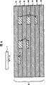
Fig. 1 has illustrated according to the ultrahigh density storage device configuration of correlation technique.Comprise the medium 1 that is divided into many memory blocks in this configuration.These memory blocks are illustrated as the square on the medium 1, and each storage area can store a data bit.
Illustrated two types storage area among Fig. 1.A kind of similar storage area comprises that general storage represents the non-modification district 2 of the data bit of value " 0 ".Another type comprises that general storage represents the modification district 3 of the data bit of value " 1 ".Typical periodically scope is between 1 and 100 nanometers between any two storage areas.
Fig. 1 is also from the conceptive emitter of having illustrated to be positioned on the medium 14, and the gap between emitter 4 and the medium 1.Emitter 4 can divergent bundle, and is configured on the removable emitter array support 5 (being also referred to as " little movable stand "), and this support can be supported the emitter 4 of hundreds and thousands of parallel-connection structures.From conceptual illustration, emitter array support 5 is provided to the electrical connection of each emitter 4 as the line on the end face of emitter array support 5.
Along with emitter 4 moves with respect to medium 1, emitter 4 can utilize high power density or low power density electron beam irradiation medium 1 lip-deep nanoscale memory block.When emission high power density beam, beam can the local material characteristics that changes irradiation area.For example, the high power density beam can produce defective in irradiated region, perhaps can the spot heating crystalline region, and this zone is cooled to the amorphous phase of same material after making.By these and other processes, can change the state (phase) of irradiated region, and emitter 4 can write medium 1 with " 1 " data bit.
When emission low power density electron beam, this Shu Buzai has the state that enough power changes material characteristics or irradiated region.Therefore, write operation does not take place.Replace, by monitoring the path of electronics in the beam, perhaps read operation can take place in the electronic effect in the beam on the irradiation area.As described below, monitor the path of electronics and/or the interaction of electronics and irradiated region can determine whether the low power density beam is just shining certain zone of medium 1, this zone before " had been write " and has been comprised " 1 " data bit now.
Specifically, be " 1 " data bit or " 0 " data bit for what determine shining, there are a plurality of options.One of these options relate to and monitor in a period of time that from the quantity of the backscattered electron beam of irradiation area, wherein when " 1 " data bit comprised that amorphous phase material and " 0 " data bit comprise the crystalline phase of same material, this option proved useful.
Because the amorphous phase of same material has different back scattered electron coefficients (BEC) with crystalline phase, when same low power density beam shines each data bit, the electronics of " 1 " in the medium 1 and " 0 " data bit backscattering varying number.Therefore, when the low power density electron beam shone certain given area, by monitoring the quantity from this backscattered electronics in zone, what might determine that this zone comprises was " 0 " data bit or " 1 " data bit.
Open in the U.S. Patent number No.5557596 that authorizes people such as Gibson (Gibson 596) some specific embodiments of above-mentioned super-high density data storage device, this patent content all is attached to herein by reference.Read technology and relate to the amorphous data bit is write the technology in the crystallization medium 1 except discussing back scattered electron, 596 patents of Gibson are also discussed various other write and read method.
Summary of the invention
A kind of data storage device, it comprises data storage medium; Be positioned near the energy of data storage medium; And the nanoscale data bit that runs through certain part of the second layer, data storage medium wherein comprises at the ground floor on medium surface and at the second layer between ground floor and the 3rd layer.
A kind of data storing method comprises provides data storage medium, by the nanoscale data bit being write the second layer with high power density beam irradiation medium, and by coming the reading of data bit with low power density beam radiation data medium, data storage medium wherein is included in the lip-deep ground floor of medium and the second layer between ground floor and the 3rd layer.
As mentioned above,, provide a kind of data storage device, comprising according to the present invention:
Data storage medium, it comprises the lamination of an alternating conductor and insulation course, makes that first conductor layer in the described conductor layer is positioned on the surface of described medium;
Be placed on the energy of described data storage medium top;
A plurality of memory blocks extend through described first conductor layer and one or more described insulation course; With
Read circuit, detect the electric current of each conductor layer when being used on the surface of described medium and be that values are selected in described a plurality of memory block according to detected each electric current in each conductor layer by described energy scanning.
Description of drawings
The present invention will be described by illustration, and the description of illustrative embodiments is specifically to carry out with reference to the accompanying drawings, wherein:
Fig. 1 has illustrated according to the top perspective of the super-high density data storage device configuration of correlation technique.
Fig. 2 has illustrated according to the cross-sectional view strength of the data storage device of the first embodiment of the present invention.
Fig. 3 has illustrated according to the perspective cutaway top view of the data storage medium of the first embodiment of the present invention.
Fig. 4 has illustrated the cross-sectional view strength of data storage device, and medium wherein comprises two conductor layers and the phase change layer between conductor layer.
Fig. 5 has illustrated the cross-sectional view strength of data storage device among Fig. 4, has wherein formed the data bit of certain state of the state of the remainder that is different from phase change layer in phase change layer.
Fig. 6 has illustrated to comprise the cross-sectional view strength of the data storage device of a plurality of conductor layers and a plurality of phase change layers.
Embodiment
Fig. 2 has illustrated according to the cross-sectional view strength of the data storage device of some embodiment of the present invention.This device comprises the energy 10 that is positioned on the data storage medium 20.Data storage medium 20 comprises the sequential cascade of conductor layer 30,50,70,90 and insulation course 40,60,80,100.Data storage medium 20 includes but not limited to: first conductor layer 30, first insulation course 40, second conductor layer 50, second insulation course 60, the 3rd conductor layer 70, the 3rd insulation course 80, the 4th conductor layer 90 and the 4th insulation course 100.
Fig. 2 has also illustrated three data bits 110,111,112.First data bit 110 comprises opening or the hole of running through first conductor layer 30 and first insulation course 40.First conductor layer 30 and first insulation course 40 are not only run through in the hole that second data bit 111 comprises, also run through second conductor layer 50, second insulation course 60, the 3rd conductor layer 70 and the 3rd insulation course 80.First conductor layer 30, first insulation course 40, second conductor layer 50 are run through in the hole of the 3rd data bit 112, and second insulation course 60.
Fig. 3 has illustrated according to the top perspective of the section part of the data storage medium 20 of some embodiment of the present invention.As shown in the figure, a plurality of conductor layers 30,50,70 and a plurality of insulation course 40,60,80 are run through in the hole of representational data bit 113.The diameter of section in hole and the size of data bit can be at nanoscale or micron orders, and bigger certainly hole also within the scope of the invention.
Fig. 3 has also illustrated one group of reometer 120, and each reometer is electrically connected to conductor layer 30,50,70.Each reometer 120 can be floated by electricity, provides bias voltage with the conductor layer 30,50,70 to its connection, and allow to monitor the magnitude of current that flows to the position that it connects from conductor layer 30,50,70.Reometer 120 can use with many embodiment of the present invention.
Can there be the upper limit as the conductor layer 30,50,70 of the part of Fig. 2 and data storage medium shown in Figure 3 and the quantity of insulation course 40,60,80,100.But some embodiment of the present invention requires to occur at least first conductor layer 30, first insulation course 40 and second conductor layer 50.
The energy 10 can comprise the energy of light energy source, heat energy and/or electron beam form.Provide the energy 10 of electron beam to occur with the form of device, for example but be not limited to such as the field emission body of Spindt emitter or such as the hot assist field emitter of Schottky (Schottky) emitter.The energy 10 generally is placed near data storage medium 20 parts (for example within 1 to 10000 nanometer).But the energy 10 and data storage medium 20 can bigger or littler at interval distances.
Although only illustrated an energy 10 among Fig. 2, many energy 10 can be placed on the parts near the surperficial part of data storage medium 20, described parts be illustrated as above-mentioned emitter array support 5, but be not limited to this.In addition, can be with not shown among Fig. 2, but one or more auxiliary energy emitters that general emission is different from the energy of beam energy be placed on the energy 10 near.The energy 10 and auxiliary energy emitter can move with respect to medium 20.But they are not limited to the displacement restriction of disclosed emitter array support 5 in 596 patents of Gibson.
Supplementary energy can also be placed near medium 20 (for example under it).This supplementary energy temperature in a certain zone of medium 20 that can be used to setover, thus make main source of energy write bit more easily, still keep high resolving power simultaneously.
In case can comprising, insulation course 40,60,80,100 forms the just material of retraction of hole.For example,, and form when running through the hole of first conductor layer 30 and first insulation course 40, can select the material contracts in first insulation course 40, thereby enlarge this hole effectively when the energy 10 usefulness high power density energy beam radiation data mediums 20.Can be by for example selecting suitable material, perhaps make first insulation course 40 be in extended state and allow internal stress to slow down, thereby promote this contraction behavior with the expansion in hole.
Perhaps, can make material evaporation or distillation by writing the energy 10 or auxiliary energy emitter, as long as material can not be deposited on the position that hinders device work (for example on the energy 10).Another alternatives is to utilize by the energy 10 fusings then because surface tension or capillary action, and the insulating material that flows away from the side forms the hole.Also having another alternatives is to write the energy 10 to produce cracking in material, or during read operation to allow polyelectron more to make described material porous to the method for darker electrode.For example can cause shrinkage, perhaps cause cracking by evaporation or distillation by the heating of the energy.
Can form two, four, six or more multi-layered data bit 110,111,112,113 running through data storage medium 20.Can be by fully heating the layer of medium 20 with the high power density energy beam, thus some material local evaporation or distillations in the layer caused, to form data bit 110,111,112,113.Owing to the irradiation of the high power density energy beam of being made up of a large amount of particles (for example electronics through being excited the electron solutions suction), data bit 110,111,112,113 can also form by the direct ablation of material.The hole can also form through flowing of fusing and material.
Selection has low melting point, low evaporating temperature and/or the insulating layer material of high-vapor-pressure at low temperatures and/or the formation that the conductor layer material can help the hole, forms the required power density of data bit 110,111,112,113 thereby can reduce.The combination that selection has the insulation of suitable wetting state and a conductor layer also can promote the formation of data bit 110,111,112,113.
Can select to utilize the energy 10 and the auxiliary energy emitter of energy beam irradiation medium 20, thereby on the surface of data storage medium 20, produce the point of micron size.But, also can select the some size of bigger or nano level energy.
Can operate the energy 10 and auxiliary energy emitter, to produce high power density beam or low power density beam.The size of selected beam power density determines that it still is write data bit 110,111,112,113 that the energy 10 or auxiliary energy emitter are used to read.
According to some embodiment, the high power density of auxiliary energy emitter emission such as the kind of energy of light or heat energy, to form the hole in medium 20, during read operation, the energy 10 is launched the low power density electron beams then.According to these embodiment, can for example carry out write operation by the near field light beam.
When the energy 10 utilizes low power density electron beam radiation data bit 110,111,112,113, do not form the hole.But read operation can take place.More particularly, if the electronics in the low power density electron beam can move to particular conductor layer 30,50,70, then will in this layer, produce marking current.
But, if being insulated layer 40,60,80, the electronics in the low power density electron beam stops, then will detect considerably less or basic detection in the conductor layer under barrier insulating layer 40,60,80 50,70,90 less than marking current.Although the layer that the sub-fraction of beam current may penetrate top layer or not remove, how far electron beam is the function of beam energy if penetrating.If utilize the low beam energy, the electric current that penetrates next conductor layer so will be negligible.
Therefore,, might determine which conductor layer the 30,50, the 70th, from the energy 10 distance of still just using electron irradiation farthest by monitoring the marking current amount in each conductor layer 30,50,70.The wisdom that should be noted that the bias voltage of each conductor layer 30,50,70 is used can to optimize at the end and is exposed the collected marking current of layer to the open air, is not reading not cause too big leakage current between the layer of electron beam simultaneously.
When carrying out read operation on the data storage medium in Fig. 3 20, have the marking current that monitors if having only in first conductor layer 30, then also do not form the hole in any layer of the data storage medium 20 below low power density electron beam irradiation part.Therefore, can distribute value for the data bit read such as " 0 ".If have the marking current that monitors separately in first conductor layer 30 and second conductor layer 50, then formed the hole of running through first conductor layer 30 and first insulation course 40 partly, therefore can be to the value of data bit distribution such as " 1 ".Other layer has been removed in the part during the process of writing, and high order dated bits then occurs, and can be to the value of its distribution such as " 2 ", " 3 " etc.Therefore, data storage medium 20 of the present invention is not limited to stores binary data.
In the embodiment that uses the energy 10 and auxiliary energy emitter, as a rule, do not utilize supplementary energy with the low power density pattern.
But some embodiment of the present invention utilizes the low power density supplementary energy really, with from medium 20 reading of data bits.According to these embodiment, each conductor layer 30,50,70,90 can replace with photoconductive material.Then, can apply bias voltage along the length of each photoelectric conductor layer, and photoconductivity that can monitoring layer (for example, at one end apply bias voltage, can at another earth terminal measuring-signal electric current).Next, if the low power density light beam arrives the specific light conductance layer, then beam increases the electric current of crossing along this laminar flow, and signal is provided.
Perhaps, conductor layer can be replaced with the luminous fluorescence coating of different wave length.Then, one or more light beams can be used to fluorescence excitation and can determine the degree of depth of the bit of writing from the spectrum of emission.In addition, above-mentioned detection scheme can also use with electron beam, and described electron beam utilizes for example cathode ray conductivity and cathode-ray luminescence rather than photoconductivity and fluorescence.
Fig. 4 has illustrated wherein, not form data storage device according to other embodiments of the invention and run through any layer hole.Device shown in Figure 4 comprises little movable stand 5, the energy 10, medium 20 and is connected to the electronic device 35 of medium 50.Medium 20 comprises first conductor layer 30, second conductor layer 50 and the phase change layer 140 between first conductor layer 30 and second conductor layer 50.This device can also comprise more than one the energy 10 and near the auxiliary energy emitter (not shown) one or more energy 10.
Fig. 5 has illustrated phase change layer 140 at the device that changes through the local state in its part material among Fig. 4 afterwards.These state variation partly are represented as the data bit 150 adjacent with first conductor layer 30.Data bit 150 can have nanometer grade diameter, micron order diameter, perhaps diameter that may be bigger, and can be along with from the energy 10 and/or from the regional area of the high power density energy beam irradiation medium 20 of auxiliary energy emitter and form.In addition, need not assist emitter, one or more resistance heated unit can be used to heat the each several part of illustration medium.These heating units should provide enough amount of localized heat, with auxiliary main station portion thermal source, do not carry out the heat of write operation but should not provide enough by himself.
Although above only discussed the material with two states, the material with two or more states also within the scope of the invention.If these materials are as the part of phase change layer 140, high order dated bits 150 more can be written in the medium 20.
Can select to be included in one or more materials in the phase change layer 140, making it at least a state is the heterogeneous body conduction.Cross (talk) when an advantage of the material of heterogeneous body conduction is to prevent from carrying out read operation in a kind of state between the data bit 150.According to some embodiment, select phase change layer 140, making it in its big resistance states is heterogeneous body, and has lower face internal conductance rate.In addition, in order to make the cross (talk) minimum between the bit, some embodiments of the present invention have also minimized the thickness of phase change layer and/or with respect to the bit-depth of bit diameter and/or the spacing between the bit.
Beam-optics arrangement can be used for the energy beam from the energy 10 and/or auxiliary energy emitter is concentrated on the nanometer or the micron order zone of medium 20.These optical devices can also be used to focus on the beam such as Fig. 2 and 3 shown devices.But they often not necessarily because energy beam self can have very little diameter, and in the hithermost place of medium, thereby benefit from proximity focusing.
As mentioned above, the write operation of the data storage device of illustrating in Fig. 4 and Fig. 5 relates to high power density energy beam radiation data medium 20.Because can make first conductor layer 30 like this, it can be penetrated by energy beam, so beam changes the state of the local part of phase change layer 140, and form data bit 150.During read operation, determine data bit 150 whether occurs in the irradiation area then.
Perhaps, writing beam can heat top conductor layer 30 and not penetrate phase change layer 140.Re conductor layer 30 will cause phase change layer 140 heating and along with heat will flow to phase change layer 140 and is modified from conductor layer 30 then.In these embodiments, conductor layer 30 should bear than the temperature required much higher temperature of state that changes phase change layer 40.In addition, the hot sheet resistance of conductor layer 30 should be quite big, makes conductor layer 30 can not cause the lateral spread of the heat affected zone size of phase change layer 140.
During read operation, the energy 10 can be with passing first conductor layer 3 but is not changed the low power density electron beam irradiation medium 20 of the partial structurtes of irradiation area.Perhaps, the electronics of most low power density electron beam can be injected between the conductor layer 30,50.
When utilizing sufficiently high beam energy, can equate so that flow into the electric current of conductor layer 30,50 from the injection electronics of reading beam.But when utilization is more low-yield, the electric current that arrives bottom conductor 50 will be lower than the electric current that arrives top conductor layer 30.Therefore, may need to monitor the electric current that arrives bottom conductor 50 in some embodiments of the invention.Electric current below conduction data bit 150 can be very little, and can be bigger at this electric current of the place that does not have data bit 150.But in general, the electric current in the bottom conductor 50 will be littler than the electric current in the top conductor layer 30, because a large amount of incoming beams of top conductor layer 30 general absorptions.
In other words, except that other factors, the quantity that is infused in the electronics between conductor layer 30 and 50 with given depth will depend on thickness and mass density, the thickness of phase change layer 140 and the energy and the intensity of mass density and beam of each conductor layer 30,50.For example, when conductor layer 30,50 keeps identical electromotive force, and be placed on the either side that has unified state and do not comprise the phase change layer of any data bit 150, to advance to conductor layer 30,50 with ratio in certain with the depth z injected electrons, this ratio is the inverse ratio of the resistance from depth z to each conductor layer 30,50.Like this, the electronics that is infused in half degree of depth between conductor 30 and 50 of half will advance to each conductor layer 30,50.On the other hand, be that 1/4 injected electrons of distance between the conductor layer 30,50 will be shunted with the degree of depth, make that 3/4 electronics advances to conductor layer 30, and other 1/4 electronics advances to another conductor layer 50.
In the phase change layer 140 of Fig. 5, the electronics that is infused in the center section of phase change layer 140 no longer makes whole phase change layer 140 have the fixed resistance rate.On the contrary, comprise the data bit 150 of the regional area of the second state material, can have higher or lower local electrical resistance rate.This phenomenon has changed the total resistance value near any specified point the data bit 150 to each conductor layer 30,50 in the phase change layer 140.In addition, will advance to conductor layer 30,50 with certain ratio at the specified point injected electrons in the phase change layer 140, this ratio is the inverse ratio of the all-in resistance between this point and each conductor layer 30,50.
If the resistance of the data bit shown in Fig. 5 150 is less than the resistance of the remainder of phase change layer 140, then less injection electronics will advance to second conductor layer 50, and electronic device 35 will detect reduced-current in second conductor layer 50.If near the resistance of the data bit 150 the second electricity level 60 is greater than the resistance of material in the remainder of phase change layer 140, otherwise then also establishment.Therefore, by local irradiation nanometer-or transverse cross-sectional area of micron diameter on phase change layer 140 surfaces, might determine to shine electronics and whether be incident on the data bit 150.Therefore, can detect data bit 150 and can be from medium 20 by electronic device 35 reading of data.
Should be noted that here what utilize is resistance notion on its broad sense, refer to the set of the physical phenomenon how influential electronics of institute to flow in medium 20, and definite they advance to which conductor layer 30,50 or electrode.For example, the length scale very short is approximately on the mean free path of electronics, this physical phenomenon set slightly different with longer length scale.Like this, the physical apparatus that is used for the read procedure of very little data bit 150 can have different slightly with the physical apparatus that is used for big bit 150.Should also be noted that if the appearance of data bit 150 produces the greater or lesser resistance interface of conductor layer 30,50, then can obtain to advance to the difference in the part of incident current of each conductor layer 30,50.For example, can form the energy barrier of Schottky barrier, charged interface or some other type with the interface of conductor layer 30,50 at a certain state (write or do not write) phase change layer 140 materials.This formation can influence the probability of the electronics that advances to conductor layer 30,50.
(not shown) can be placed on phase change layer and resistive layer between top conductor layer and the bottom conductor according to other embodiments of the invention.The resistivity of resistive layer can be fixed on the crystalline state of phase change layer and the intermediate value between the amorphous state resistivity.The application of this configuration can improve writing of phase change layer and not write signal difference between the zone.
Fig. 6 has illustrated according to another embodiment of data storage device of the present invention.Device shown in Figure 6 comprises the energy 10 that can be placed on little movable stand 5, and can comprise data storage layer 20, the layer 20 several phase change layer 140,160,180 that comprises between several conductor layers 30,50,70,90 itself.
Can be with mode like the device class of operation shown in the Figure 4 and 5, nearest three layer 30,140,50 of the energy emitter in device shown in Figure 6 10 operated.For example, the data bit 150 in Fig. 6 left side comprises the local material zone under second state, and this area part runs through the phase change layer 140 under first state.When with the irradiation of low power density electron beam, can detect data bit 150 by the relative intensity that monitors marking current in first conductor layer 30 and second conductor layer 50 once more.
But the device among Fig. 6 comprises additional phase change layer 160,180, and extra conductor layer 70,90, and data bit 155,157, these data bits run through first phase change layer 140 fully and part runs through at least one other phase change layer 160,180.In alternative, data bit 155,157 does not change the accumulation layer state of going up.Device among Fig. 6 can change the difference in the ratio of the marking current that flows to two conductor layers adjacent with phase change layer, and described phase change layer comprises the part from first phase change layer 140 data bit 150,155,157 farthest.
In operation, the one or more energy 10 or auxiliary energy emitter can be used to high power density energy beam irradiation medium 20.These beams can penetrate a plurality of layers of medium 20, depend on material behavior, beam energy of each layer etc., and therefore can be with the part of state layer 140,160,180 from first state-transition to second state, thereby write data bit 150,155,157.
During read operation, the energy 10 can be launched penetrable medium 20, and the low power density electron beam of any phase change layer 140,160,180 shown in electronics can being injected.In case electronics is injected in the not change part of phase change layer 140,160,180 or near, the behavior of electronics and electrical type shown in Figure 4 seemingly and can detect the part that do not write of phase change layer.
When electronics be injected in second state part of phase change layer 140,160,180 or near, on nearest, cover when extending fully between conductor layer and the nearest following covering conductor layer, the behavior of electronics is similar when not having second phase change portion fully.In fact, there do not have the path to become because of the appearance of second state part to be best relatively, and electronics will advance to any adjacent conductive layers, just as they are advanced when not having the second state part.
But when electronics is injected into when only having part and running through in the phase change layer 140,160,180 of the second state material of phase change layer, the described electrical type of the behavior of electronics and Fig. 5 seemingly and can detect data bit 150,155,157.
When medium shown in Figure 6 20 reads, to being surrounded when not showing by recording phase change layer, detect " 0 " data bit as their in all adjacent conductive layers.When the second state material only partly ran through phase change layer 140, this can represent to occur data bit 150 and read like " 1 " data bit.When only detecting part and run through the second state material of the phase change layer 160 between second conductor layer 50 and the 3rd conductor layer 70, whole first phase change layer 140 may occur running through also only partly runs through the data bit 155 of second phase change layer 160, and is pronounced " 2 " data bit." 3 " data bit 157 will detect for part only run through between the 3rd conductor layer 70 and the 4th conductor layer 90 phase change layer 180 with and go up the second state material of all phase change layers 140,160.
Also may write down the non-binary data bit by only utilizing the single phase change memory between the pair of conductors layer.This can finish by the part of the altered accumulation layer of change state.For example, " 1 " data bit can run through 1/3rd distances of accumulation layer, and " 2 " data bit can run through 2/3rds distances of accumulation layer.Like this, the current segment difference of different pieces of information bit, and detected difference between current can be used to the value of specified data bit in the adjacent conductive layers.
Device shown in Fig. 4-6 can be rewritable, also can rewrite, and depends on whether the variation between first state and second state is reversible in the phase change layer 140,160,180.If state variation is reversible, can be written into many times according to the data storage device of these embodiment, this also provides another advantage.
Above detailed description just is used to understand illustration of the present invention and realizes, should be appreciated that the present invention does not have unnecessary restriction, because for a person skilled in the art, modification is conspicuous, does not deviate from the scope of appended claims and equivalent thereof.
Claims (7)
1. data storage device comprises:
Data storage medium (20), it comprises the lamination of an alternating conductor (30,50,70,90) and insulation course (40,60,80,100), makes that first conductor layer (30) in the described conductor layer (30,50,70,90) is positioned on the surface of described medium (20);
Be placed on the energy (10) of the surface of described data storage medium (20);
A plurality of nanoscales memory block (110,111,112) extends through described first conductor layer (30) and one or more described insulation course; With
Read circuit (35,120), be used for detecting when being scanned by the described energy (10) electric current of each conductor layer and be that the value that will store is selected in described a plurality of nanoscales memory block according to detected each electric current in each conductor layer on the surface of described medium.
2. data storage device as claimed in claim 1 is characterized in that, at least one in the described insulation course (140) comprises one first district and one second district, and described first district comprises phase-change material; Described second district comprises resistance material, the resistivity value of described resistance material is a value between the resistivity value of second state of first state of described phase-change material and described phase-change material, and wherein said first state is that crystalline phase and described second state are amorphous phases.
3. data storage device as claimed in claim 1 is characterized in that, at least one in the described insulation course (40,140) comprises thermal insulation material.
4. data storage device as claimed in claim 1 is characterized in that, the described energy comprises at least one in field emission body, Spindt emitter and the Schottky emitter.
5. data storage device as claimed in claim 1 is characterized in that, at least one in the described insulation course (140) comprises phase-change material.
6. data storage device as claimed in claim 1 is characterized in that, at least one in the described insulation course (140) comprises two kinds of different phase-change materials.
7. data storage device as claimed in claim 1 is characterized in that containing plural conductor layer (30,50,70,90), and described a plurality of nanoscales memory block can be stored than the binary value data bit value of high-order more.
Applications Claiming Priority (2)
| Application Number | Priority Date | Filing Date | Title |
|---|---|---|---|
| US09/984419 | 2001-10-30 | ||
| US09/984,419 US7102983B2 (en) | 2001-10-30 | 2001-10-30 | Current divider-based storage medium |
Publications (2)
| Publication Number | Publication Date |
|---|---|
| CN1417784A CN1417784A (en) | 2003-05-14 |
| CN100474421C true CN100474421C (en) | 2009-04-01 |
Family
ID=25530541
Family Applications (1)
| Application Number | Title | Priority Date | Filing Date |
|---|---|---|---|
| CNB021499020A Expired - Fee Related CN100474421C (en) | 2001-10-30 | 2002-10-30 | Memory medium based on current distribution |
Country Status (4)
| Country | Link |
|---|---|
| US (1) | US7102983B2 (en) |
| EP (1) | EP1308946A3 (en) |
| JP (1) | JP2003187505A (en) |
| CN (1) | CN100474421C (en) |
Families Citing this family (4)
| Publication number | Priority date | Publication date | Assignee | Title |
|---|---|---|---|---|
| NL1022855C2 (en) * | 2003-03-05 | 2004-09-07 | Univ Delft Tech | Method and device for the controlled manufacture of openings on a nanometer scale. |
| US7074707B2 (en) * | 2003-09-15 | 2006-07-11 | International Business Machines Corporation | Method of fabricating a connection device |
| US7184388B2 (en) * | 2004-03-09 | 2007-02-27 | Hewlett-Packard Development Company, L.P. | Heating elements for a storage device |
| US7277314B2 (en) * | 2004-05-27 | 2007-10-02 | Cabot Microelectronics Corporation | Mobile ion memory |
Family Cites Families (22)
| Publication number | Priority date | Publication date | Assignee | Title |
|---|---|---|---|---|
| US4090031A (en) * | 1974-10-21 | 1978-05-16 | Eli S. Jacobs | Multi-layered opitcal data records and playback apparatus |
| US4427886A (en) * | 1982-08-02 | 1984-01-24 | Wisconsin Alumni Research Foundation | Low voltage field emission electron gun |
| JPS59163506A (en) * | 1983-03-09 | 1984-09-14 | Hitachi Ltd | Electronic beam measuring device |
| US4534016A (en) * | 1983-07-08 | 1985-08-06 | The United States Of America As Represented By The Secretary Of The Air Force | Beam addressed memory system |
| JPS62246158A (en) | 1986-04-19 | 1987-10-27 | Victor Co Of Japan Ltd | Information recording medium |
| JPS6318541A (en) * | 1986-07-11 | 1988-01-26 | Hitachi Ltd | Electron beam recording and reproducing method and its apparatus |
| US4760567A (en) * | 1986-08-11 | 1988-07-26 | Electron Beam Memories | Electron beam memory system with ultra-compact, high current density electron gun |
| JPS63316336A (en) | 1987-06-18 | 1988-12-23 | Fujitsu Ltd | Electron ray disk |
| US5216631A (en) * | 1990-11-02 | 1993-06-01 | Sliwa Jr John W | Microvibratory memory device |
| JPH0536128A (en) * | 1990-12-20 | 1993-02-12 | Hitachi Ltd | High density information recording medium and recording device using this |
| US5537372A (en) * | 1991-11-15 | 1996-07-16 | International Business Machines Corporation | High density data storage system with topographic contact sensor |
| JPH06251435A (en) * | 1993-03-01 | 1994-09-09 | Canon Inc | Recording and reproducing device |
| US5557596A (en) * | 1995-03-20 | 1996-09-17 | Gibson; Gary | Ultra-high density storage device |
| US5724336A (en) * | 1995-04-25 | 1998-03-03 | Morton; Steven G. | Tera-byte disk drive |
| US5835477A (en) * | 1996-07-10 | 1998-11-10 | International Business Machines Corporation | Mass-storage applications of local probe arrays |
| FR2757992B1 (en) * | 1996-12-26 | 1999-01-29 | Commissariat Energie Atomique | INFORMATION RECORDING MEDIUM, DEVICE FOR READING THE MEDIA, AND METHODS OF IMPLEMENTING THE DEVICE |
| JP3477024B2 (en) * | 1997-02-25 | 2003-12-10 | 株式会社東芝 | Recording medium, recording method, erasing method, reproducing method, recording / reproducing method, reproducing apparatus, and recording / reproducing apparatus |
| US5936243A (en) * | 1997-06-09 | 1999-08-10 | Ian Hardcastle | Conductive micro-probe and memory device |
| JPH11120634A (en) | 1997-10-09 | 1999-04-30 | Nobuyuki Higuchi | Information recording medium and information reading device |
| DE10029593A1 (en) * | 1999-07-03 | 2001-01-18 | Ibm | Recording and reproducing data on storage medium in which storage medium is part of read/write signal path |
| JP3688530B2 (en) | 1999-09-29 | 2005-08-31 | 株式会社東芝 | Recording medium, recording apparatus, and recording method |
| US7054256B2 (en) * | 2000-10-20 | 2006-05-30 | Ochoa Optics Llc | High capacity digital data storage by transmission of radiant energy through arrays of small diameter holes |
-
2001
- 2001-10-30 US US09/984,419 patent/US7102983B2/en not_active Expired - Fee Related
-
2002
- 2002-10-16 JP JP2002301498A patent/JP2003187505A/en active Pending
- 2002-10-30 EP EP02257519A patent/EP1308946A3/en not_active Withdrawn
- 2002-10-30 CN CNB021499020A patent/CN100474421C/en not_active Expired - Fee Related
Also Published As
| Publication number | Publication date |
|---|---|
| EP1308946A3 (en) | 2004-10-13 |
| JP2003187505A (en) | 2003-07-04 |
| EP1308946A2 (en) | 2003-05-07 |
| US20030081533A1 (en) | 2003-05-01 |
| US7102983B2 (en) | 2006-09-05 |
| CN1417784A (en) | 2003-05-14 |
Similar Documents
| Publication | Publication Date | Title |
|---|---|---|
| JP5313522B2 (en) | Multi-level data storage device with phase change material | |
| Gidon et al. | Electrical probe storage using Joule heating in phase change media | |
| KR100724513B1 (en) | Probe for scanning over a substrate and data storage device | |
| US8796596B2 (en) | Heater and memory cell, memory device and recording head including the heater | |
| US6473388B1 (en) | Ultra-high density information storage device based on modulated cathodoconductivity | |
| JP4234077B2 (en) | Data storage device and method for reading data in the data storage device | |
| CN100474421C (en) | Memory medium based on current distribution | |
| EP1251503A2 (en) | Data storage device | |
| US7414953B2 (en) | Memory having a layer with electrical conductivity anisotropy | |
| US7379412B2 (en) | Methods for writing and reading highly resolved domains for high density data storage | |
| US20090175153A1 (en) | Electrical-Effect Data Recording Medium that Includes a Localized Electrical Conduction Layer | |
| US7027380B2 (en) | Atomic resolution storage device | |
| US7209429B2 (en) | Data recording device comprising micro-tips and a recording medium | |
| US7301887B2 (en) | Methods for erasing bit cells in a high density data storage device | |
| US6872964B2 (en) | Data storage device | |
| EP1756808A2 (en) | Methods for writing and reading highly resolved domains for high density data storage | |
| JP2010056556A (en) | Data storage device by optical addressing | |
| Serra | Toward the Next generation of Non Volatile Phase-Change Memory Targeting Ultra-Low Power Consumption | |
| US20070008863A1 (en) | Memory comprising a memory device and a write unit configured as a probe | |
| US7082095B2 (en) | System and method for storing data | |
| US6937502B2 (en) | Re-recordable data storage medium utilizing conduction barrier | |
| Vettiger et al. | The “Millipede”—More than 1000 tips for future scanning-probe data storage | |
| CN1816861A (en) | Device and method for making a master record carrier for use in making a stamper | |
| Murashita | Conductive transparent probes and their application to high-density phase-change data storage by using current injection | |
| US20050243660A1 (en) | Methods for erasing bit cells in a high density data storage device |
Legal Events
| Date | Code | Title | Description |
|---|---|---|---|
| C06 | Publication | ||
| PB01 | Publication | ||
| C10 | Entry into substantive examination | ||
| SE01 | Entry into force of request for substantive examination | ||
| C14 | Grant of patent or utility model | ||
| GR01 | Patent grant | ||
| C17 | Cessation of patent right | ||
| CF01 | Termination of patent right due to non-payment of annual fee |
Granted publication date: 20090401 Termination date: 20111030 |