CN100474440C - Magnetic memory device and method - Google Patents
Magnetic memory device and method Download PDFInfo
- Publication number
- CN100474440C CN100474440C CNB031360440A CN03136044A CN100474440C CN 100474440 C CN100474440 C CN 100474440C CN B031360440 A CNB031360440 A CN B031360440A CN 03136044 A CN03136044 A CN 03136044A CN 100474440 C CN100474440 C CN 100474440C
- Authority
- CN
- China
- Prior art keywords
- layer
- magnetic
- orientation
- ferromagnetic
- memory device
- Prior art date
- Legal status (The legal status is an assumption and is not a legal conclusion. Google has not performed a legal analysis and makes no representation as to the accuracy of the status listed.)
- Expired - Lifetime
Links
Images


Classifications
-
- B—PERFORMING OPERATIONS; TRANSPORTING
- B82—NANOTECHNOLOGY
- B82Y—SPECIFIC USES OR APPLICATIONS OF NANOSTRUCTURES; MEASUREMENT OR ANALYSIS OF NANOSTRUCTURES; MANUFACTURE OR TREATMENT OF NANOSTRUCTURES
- B82Y25/00—Nanomagnetism, e.g. magnetoimpedance, anisotropic magnetoresistance, giant magnetoresistance or tunneling magnetoresistance
-
- G—PHYSICS
- G11—INFORMATION STORAGE
- G11C—STATIC STORES
- G11C11/00—Digital stores characterised by the use of particular electric or magnetic storage elements; Storage elements therefor
- G11C11/02—Digital stores characterised by the use of particular electric or magnetic storage elements; Storage elements therefor using magnetic elements
- G11C11/16—Digital stores characterised by the use of particular electric or magnetic storage elements; Storage elements therefor using magnetic elements using elements in which the storage effect is based on magnetic spin effect
-
- H—ELECTRICITY
- H01—ELECTRIC ELEMENTS
- H01F—MAGNETS; INDUCTANCES; TRANSFORMERS; SELECTION OF MATERIALS FOR THEIR MAGNETIC PROPERTIES
- H01F10/00—Thin magnetic films, e.g. of one-domain structure
- H01F10/32—Spin-exchange-coupled multilayers, e.g. nanostructured superlattices
- H01F10/324—Exchange coupling of magnetic film pairs via a very thin non-magnetic spacer, e.g. by exchange with conduction electrons of the spacer
- H01F10/3254—Exchange coupling of magnetic film pairs via a very thin non-magnetic spacer, e.g. by exchange with conduction electrons of the spacer the spacer being semiconducting or insulating, e.g. for spin tunnel junction [STJ]
-
- H—ELECTRICITY
- H01—ELECTRIC ELEMENTS
- H01F—MAGNETS; INDUCTANCES; TRANSFORMERS; SELECTION OF MATERIALS FOR THEIR MAGNETIC PROPERTIES
- H01F10/00—Thin magnetic films, e.g. of one-domain structure
- H01F10/32—Spin-exchange-coupled multilayers, e.g. nanostructured superlattices
- H01F10/324—Exchange coupling of magnetic film pairs via a very thin non-magnetic spacer, e.g. by exchange with conduction electrons of the spacer
- H01F10/3268—Exchange coupling of magnetic film pairs via a very thin non-magnetic spacer, e.g. by exchange with conduction electrons of the spacer the exchange coupling being asymmetric, e.g. by use of additional pinning, by using antiferromagnetic or ferromagnetic coupling interface, i.e. so-called spin-valve [SV] structure, e.g. NiFe/Cu/NiFe/FeMn
- H01F10/3272—Exchange coupling of magnetic film pairs via a very thin non-magnetic spacer, e.g. by exchange with conduction electrons of the spacer the exchange coupling being asymmetric, e.g. by use of additional pinning, by using antiferromagnetic or ferromagnetic coupling interface, i.e. so-called spin-valve [SV] structure, e.g. NiFe/Cu/NiFe/FeMn by use of anti-parallel coupled [APC] ferromagnetic layers, e.g. artificial ferrimagnets [AFI], artificial [AAF] or synthetic [SAF] anti-ferromagnets
- H01F10/3277—Exchange coupling of magnetic film pairs via a very thin non-magnetic spacer, e.g. by exchange with conduction electrons of the spacer the exchange coupling being asymmetric, e.g. by use of additional pinning, by using antiferromagnetic or ferromagnetic coupling interface, i.e. so-called spin-valve [SV] structure, e.g. NiFe/Cu/NiFe/FeMn by use of anti-parallel coupled [APC] ferromagnetic layers, e.g. artificial ferrimagnets [AFI], artificial [AAF] or synthetic [SAF] anti-ferromagnets by use of artificial ferrimagnets [AFI] only
Abstract
The present invention is a magnetic memory device and method. In one embodiment a present invention magnetic memory device includes a synthetic ferrimagnetic data, a soft reference layer and a tunneling layer. The synthetic ferrimagnetic data layer has a magnetic moment directable to a first orientation and a second orientation. The soft reference layer has a lower coercivity than the synthetic ferrimagnetic data layer. The tunneling layer has electrical resistance qualities which are influenced by magnetic moment orientations of the synthetic ferrimagnetic data layer and the soft reference layer.
Description
Technical field
The present invention relates to a kind of memory device, particularly, the present invention relates to magnetic memory device.
Background technology
Electronic system and circuit have been made remarkable contribution and have been used in the extensive application to realize favourable outcome towards the progress of modern science.Various electronic technology such as digital machine, counter, acoustic apparatus, video equipment and telephone system have been beneficial on analysis and propagation data, idea and trend in most of fields of commerce, science, education and dinner party and have boosted productivity and reduce cost.Usually, these favourable outcomes are to be stored in the storage medium and by the information that treating apparatus is controlled by employing to realize.The structure and the type that are used for the storer of store information may have sizable impact to the information processing performance.
Various electronic installations comprise the processor of operating by executive routine, and these programs comprise a series of instructions of the data that are used for controlling the available task performance.This program and related data are stored in the storage unit with unique indicator or address usually.But the effectiveness that treating apparatus provides depends on the quantity of information and its speed of access of memory stores usually.Access memory reaches the ability that transmits information fast and expediently has sizable impact to the information processing stand-by period usually.
Magnetic storage is one type the storer that lot of advantages is provided usually.For example, magnetic storage is carried out the read and write operation than short-term and long term memory such as dynamic RAM (DRAM), synchronous RAM (SRAM), the flash memory of other type with conventional hard disc drive is faster and the power of consumption is also low than it.Magnetic storage can also be carried out the read and write operation quickly than conventional long-term storage devices such as hard disk drive usually.In addition, magnetic storage is compacter and be convenient to store more information in littler space than the legacy memory of other type usually.
Typical MRAM device comprises the memory cell array of the bit line that has the word line that extends along the row of storage unit and extend along the row of storage unit.Each memory cell is positioned at the place, point of crossing of word line and bit line.Storage unit is become the basis with tunnel magnetoresistive (TMR) device as spin-dependent tunneling (SDT) usually.Tradition SDT knot comprise pinning layer, readout layer and be clipped in pinning layer and readout layer between the insulating tunnel restraining barrier.Pinning layer has magnetization orientation, and its magnetization orientation is fixed so that do not rotate under the situation that applies magnetic field intensity in having limited range.Readout layer has can be in the magnetization of promptly identical or opposite with the pinning layer magnetization orientation direction orientation of one of both direction.
The magnetization orientation of pinning layer is fixed by the anti-ferromagnetic material of lower floor (AF) pinning layer usually.Pinning layer in some traditional magnetoresistive memory device may have Net magnetic moment, and this causes undesirable effect.And this effect is the demagnetizing field effect.For example, too strong if magnetic field becomes, interact from the magnetic field arrival of pinning layer and with mode and the readout layer that causes data degradation.In addition, the state that exists the magnetic field from pinning layer to cause usually being used for the translation data layer uses asymmetric magnetic field, and this has generally increased the complicacy of the process of writing.Because the tolerance of stray magnetic field has reduced during writing, therefore often also further complicacy can appear.
Summary of the invention
The present invention relates to magnetic memory device and method.In one embodiment, magnetic memory device of the present invention comprises synthetic ferromagnetic data layer, soft reference layer and tunnel layer.Synthetic ferromagnetic data layer has the magnetic moment that can point to first orientation and second orientation.Soft reference layer has the coercive force lower than synthetic ferromagnetic data layer.Tunnel layer has the resistive by the magnetic moment orientation influence of synthetic ferromagnetic data layer and soft reference layer.
Description of drawings
Fig. 1 represents the block scheme of magnetic memory device according to an embodiment of the invention.
Fig. 2 A represents to have an example of the synthetic ferromagnetic sublayer of the magnetic moment of orientation in the opposite direction.
Fig. 2 B represents to keep an example of the synthetic ferromagnetic sublayer of opposite relatively magnetic moment orientation when the orientation reversing.
Fig. 3 is the view that is illustrated in the exemplary coercive force relation between hard data layer and the soft reference layer.
Fig. 4 represents the process flow diagram of magnetic storage method according to an embodiment of the invention.
Fig. 5 represents magnetic RAM (MRAM) device as an exemplary enforcement of memory device of the present invention.
Fig. 6 A represents the exemplary variations of the orientation of the magnetic moment relevant with the respective change of pulse signal.
Fig. 6 B illustrates the synoptic diagram of pulse signal according to an embodiment of the invention.
Fig. 6 C represents to respond magnetic moment orientation owing to the exemplary final resistance that the response impulse signal changes reduces.
Fig. 7 A is another exemplary diagram of the exemplary variation of the magnetic moment orientation relevant with the response change of pulse signal.
Fig. 7 B is another exemplary diagram of exemplary pulse signal according to an embodiment of the invention.
Fig. 7 C represents to respond magnetic moment orientation owing to the exemplary final resistance that the response impulse signal changes increases.
Embodiment
Below with reference to the preferred embodiments of the present invention is that magnetic memory systems and method are elaborated, and example of the present invention has been shown in the accompanying drawing.Though the present invention will be described in conjunction with the preferred embodiments, should be appreciated that scope of the present invention is not limited to these embodiment.On the contrary, the present invention is tending towards covering replacement, modification and the equivalents that is comprised in the spirit and scope of the present invention that limited by appended claims.And, in the detailed description of the present invention below,, provided a large amount of details for complete understanding of the present invention is provided.But, should be appreciated that the present invention can implement under the situation of these details not having.In other words, known method, program, element and circuit no longer describe in detail, so that the solution of the present invention is fuzzy.
The present invention is beneficial to convenient and effectively utilizes magnetic storage systems and method canned data.In one embodiment, magnetic memory device of the present invention comprises hard synthetic ferromagnetic data (a.k.a. reads) layer and soft synthetic ferromagnetic reference layer.Term hard and soft be relative, and have been interpreted as using easily and avoid making the present invention unclear, so for illustrative purposes, term " hard relatively " or " soft relatively " abbreviate " firmly " or " soft " as.Utilize synthetic ferromagnetic layer to be convenient to when the magnetic layers of composition data layer and/or reference layer, adopt identical magnetic material.This minimizes structure and the specific number of growth machine, and this specificity is influential to the correct crystal orientation that obtains.
Fig. 1 represents the block scheme of magnetic memory device 10 according to an embodiment of the invention.In a signal embodiment, magnetic memory device 10 is storage unit.Magnetic memory device 10 comprises magnetic tunnel-junction 11, and this tunnel junction 11 has synthetic ferromagnetic data layer 12, soft reference layer 14 and the tunnel barrier layer 16 between synthetic ferromagnetic data layer 12 and soft reference layer 14.Synthetic ferromagnetic data layer 12 is coupled to tunnel barrier layer 16, and tunnel barrier layer 16 is coupled to soft reference layer 14.Synthetic ferromagnetic data layer 12 also is called readout layer and has the magnetic moment that can point to first and second orientations.The magnetization (M1 represents by vector) of synthetic ferromagnetic data layer 12 and the magnetization (being represented by M2) of soft reference layer 14 are dynamically controlled so that basically in one of both direction orientation (for example along transverse axis, as the EAI of data Layer 12).For example, tunnel barrier layer 16 allows to produce the quantum mechanical tunnel effect between synthetic ferromagnetic data layer 12 and soft reference layer 14, wherein the influence that the final resistance of the electric current that vertically applies is subjected to synthesizing the ferromagnetic data layer 12 and the relative magnetic moment orientation of soft reference layer 14.
Synthetic ferromagnetic data layer 12 and soft reference layer 14 can comprise various materials.For example, soft reference layer 14 can be by ferromagnetic material or the synthetic ferromagnetic material (SF) that also is known as artificial antiferromagnet constitute.Synthetic ferromagnetic data layer 12 also has different coercive forces with soft reference layer 14.For example, reference layer 14 is than " firmly " data Layer 12 (for example having higher coercive force) " soft " (for example having lower coercive force).The easy degree that the magnetic moment orientation of coercive force influence layer changes.For example, relatively easily change the magnetic moment orientation of soft formation (for example having " weak " magnetic field that produces by the little electric current that in conductor, flows).
The tunnel(l)ing of tunnel barrier layer 16 is relevant with electron spin, and the resistance that makes magnetic tunnel-junction 11 is the function of relative orientation of the magnetization vector (M1 and M2) of data Layer and reference layer 12 and 14.For example, if the relative orientation of magnetization vector (for example M1 and M2) is identical, then the resistance to the magnetic tunnel-junction 11 that vertically applies electric current (for example mobile or vice versa to soft reference layer 14 by tunnel barrier layer 16 from synthetic ferromagnetic data layer 12) is first value (for example R), if magnetization orientation on the contrary then be second value.Tunnel barrier layer 16 can be made by various media and semiconductor material, comprises aluminium oxide (Al
2O
3), silicon dioxide (SiO
2), tantalum oxide (Ta
2O
5), silicon nitride (Si
3N
4), aluminium nitride (AlN
x) and/or magnesium oxide (MgO).The thickness of tunnel barrier layer 16 can be within the specific limits (for example from about 0.5 nanometer to about 3 nanometers) changes.The present invention is not necessarily limited to particular tunnel and stops scope.
Utilize of the storage of two different resistance states of magnetic tunnel-junction 11 with indication logic place value.For example, when the orientation of synthesizing the ferromagnetic data layer 12 and the magnetization vector of soft reference layer 14 is identical, to the resistance that vertically applies electric current in the first resistance value scope of corresponding first predetermined logic values (for example " 0 "), when opposite orientation, to the resistance that vertically applies electric current in the second resistance value scope of corresponding second predetermined logic values (for example " 1 ").If the magnetization vector M1 of synthetic iron data Layer 12 and the magnetization vector M2 of soft reference layer 14 point to substantially the same direction, then the orientation of magnetic tunnel-junction 11 can be called " parallel ".If magnetization vector M1 and M2 point to opposite basically direction, then the orientation of magnetic tunnel-junction 11 can be called " antiparallel ".The resistance value of corresponding two magnetic alignings (parallel with antiparallel) can be relevant with logical value (for example " 0 " and " 1 ").The logical value of being represented by the specific orientation structure is predetermined arbitrarily in one embodiment.
The invention is not restricted to two-layer magnetization orientation and be parallel or antiparallel relative to each other.In general, every layer magnetization orientation can so be selected, so that the measured resistance range between the layer is different for two distinguishable states.In a signal embodiment, first state comprises first stable orientations, and second state comprises second stable orientations.For example, synthetic ferromagnetic readout layer is exercisable for the magnetization of one of two distinguishable states.Two distinguishable states are relevant with two stable orientations, and can be included in the first scope angle and the second scope angle between the magnetization orientation vector M2 of the magnetization orientation vector M1 of synthetic ferromagnetic data layer 12 and soft reference layer 14, wherein the resistance at tunnel layer two ends has first resistance range and second resistance range of corresponding two stable magnetic moment orientations.The resistance of electric current is changed according to the relative direction with respect to first or second magnetic aligning of the synthetic ferromagnetic data layer 12 of the magnetic aligning of soft reference layer 14.
Data Layer in the magnetic memory device 10 and the magnetic aligning of reference layer quilt and one group of electromagnetic field control that electrical conductive elements is relevant.Still referring to Fig. 1, first conductor 18 that extends along the x axle is coupled to synthetic ferromagnetic data layer 12.Second conductor 20 that extends along the yz axle is coupled to soft reference layer 14.First and second conductors 18 that illustrate and 20 perpendicular (though the invention is not restricted to vertical orientated).Be the 3rd conductor 22 (for example reading conductor) below second conductor 20, it also extends along the y axle.Electrical insulator 24 (for example one deck dielectric material) separates the second and the 3rd conductor 20 and 22.Conductor (for example 18,20 and 22) can comprise various conductive materials, comprises aluminium, copper, gold or silver-colored.Apply electric current by the specific direction on conductor (for example conductor 18,20 and/or 22), data Layer and/or reference layer are exposed to the electromagnetic field that is produced by the electric current in the conductor.The magnetic that applies the magnetic field of sufficient intensity and data Layer and reference layer to set up that electromagnetic principle is consistent (for example right hand rule) and be known.
Fig. 2 A and 2B represent an example of synthetic ferromagnetic layer 59, and it comprises and is spaced apart the first and second ferromagnetic sublayers 50 and 52 that sublayer 54 (wall 54 can be a metal) separates.In an example, first sublayer has the magnetic moment orientation that can be rotated to first or second orientation, and spacer sublayer first and second sublayers that magnetically are coupled, so that second sublayer has the basic maintenance magnetic orientation opposite with first sublayer.Ferromagnetic sublayer 50 and 52 can be made of various materials, comprise iron cobalt (CoFe), ferronickel (NiFe), cobalt (Co) etc., spacer sublayer 54 can be made of the conduction nonmagnetic substance, comprises ruthenium (Ru), rhenium (Re), rhodium (Rh), copper (Cu), tellurium (Te), chromium (Cr) etc.In an exemplary embodiment, the thickness of spacer sublayer is in about 0.2nm-2nm scope, and each ferromagnetic sublayer 50 and 52 coercive force are in about 10-100Oe scope and have an identical shaped magnetic hysteresis loop.
The magnetization vector of two ferromagnetic sublayers or the exchange coupling between the magnetic moment orientation are very strong.Thereby, will need very large magnetic field (for example 4000 Oe) with " decoupling " magnetization vector and the retentivity that overcomes the basic opposite magnetic moment in ferromagnetic sublayer 50 and 52.For example, the field (for example 3.2 * 10 that needs 4000 oersteds
5Amperes per meter) to rotate the magnetic moment orientation of two ferromagnetic layers 50 and 52 fully at equidirectional.By selecting to be used for the suitable thickness and the material of wall 54, but proper strength ground carries out exchange coupling, so that under normal operating condition, produces very little decoupling or rotation, and the magnetic moment vector of ferromagnetic layer 50 and 52 points to basically to be separated by and 180 spends.
Total or the Net magnetic moment of synthetic ferromagnetic layer is determined by the difference of the magnetic moment of ferromagnetic sublayer.For example, total magnetic moment (M of synthetic ferromagnetic layer 59
SF) equal the magnetic moment (M of the first ferromagnetic sublayer 50
FM1) deduct the magnetic moment (M of the second ferromagnetic sublayer 52
FM2).This relation can be by equation M
SF=M
FM1-M
FM2Expression.Imbalance of the present invention (not waiting) magnetic moment M1 and M2 cause total non-zero magnetic moment.Low-coercivity allows the total magnetization vector (for example M2) of SF layer (for example reference layer 14) to be easy to change between the orientation shown in Fig. 2 A and the 2B.
Select the material and the yardstick (for example thickness) of spacer sublayer 54 to make first and second sublayers 50 and 52 magnetic couplings, so that their magnetic aligning is opposite basically or antiparallel.For example, Fig. 2 A represents along the magnetization vector M2A of the last sublayer 52 of negative y axle orientation with along the magnetization vector M2B of the following sublayer 50 that positive y axle is orientated.The thickness of wall 54 can be depending on the material that is included in the wall 54.For example, the thickness of spacer sublayer 54 can be between about 0.2nm-2nm.
In one embodiment of the invention, synthetic ferromagnetic layer has the basic sublayer that the resistance of measuring in data Layer, magnetic channel restraining barrier and basic sublayer (for example the sublayer 50) is passed in influence.Utilize the magnetic moment orientation or the direction of measuring resistance specified data layer.In one embodiment, the basic the most close tunnel barrier layer in sublayer (for example tunnel barrier layer 16).At a signal embodiment, with reference to orientation conductor (for example the 3rd conductor 22) than another sublayer of synthetic ferromagnetic layer further from a ferromagnetic sublayer (for example 50 or 52).Like this, the magnetic aligning of each sublayer can know that this direction partly depends on the sense of current by each conductor (for example the 3rd conductor 22) by direction of its preference in each ferromagnetic sublayer.
In one embodiment of the invention, the coercive force of synthetic ferromagnetic (SF) layer is low.For example, the coercive force of synthetic ferromagnetic (SF) layer (for example synthetic magnetic reference layer) is lower than another layer (for example synthesizing magnetic data Layer), and relatively high coercivity layer is soft than the synthetic ferromagnetic layer of low-coercivity.For example, the ultralow coercive force in the SF layer allows the magnetization vector (M2A and M2B) of SF layer (for example reference layer 14) to be easy to conversion between orientation (for example shown in Fig. 2 A and the 2B).In fact, just before applying magnetic field, ferromagnetic layer 50 and 52 magnetic moment vector M2A and the orientation of M2B can be in any basic opposite direction.In case applied magnetic field, their oriented is set up electromagnetic principle (for example right-hand rule) and is known.Because the coercive force of synthetic ferromagnetic layer is low, therefore putting on ferromagnetic layer 50 pushes magnetic vector M2A and M2B to known position (for example perpendicular to applying magnetic field) with 52 relative little magnetic field.Reference layer can comprise synthetic ferromagnetic layer, and this layer is configured the Net magnetic moment (for example net magnetization vector) that is substantially zero to have.For example, reference layer can comprise and equating basically and opposite a plurality of magnetization vectors (for example magnetization vector M2A and M2B), therefore can cancel each other basically on a distance.
In one embodiment of the invention, the coercive force of synthetic ferromagnetic (SF) layer is high relatively.For example, the coercive force of synthetic ferromagnetic (SF) layer (for example synthesizing magnetic data Layer) is than other layer (for example synthesizing magnetic reference layer) height, and higher coercivity is synthesized ferromagnetic layer, and relatively low coercivity layer is hard.The high-coercive force of SF layer can make and keep orientation (for example shown in Fig. 2 A and 2B) under the magnetization of SF layer (for example data Layer 12) or the situation that magnetic moment vector (M2A and M2B) is not changed when being exposed to downfield.In fact, when being exposed to enough strong magnetic field, set the magnetization vector M2A of ferromagnetic layer 50 and 52 and the orientation of M2B.In case apply magnetic field, their oriented is set up electromagnetic principle and is known.Because the coercive force height of synthetic ferromagnetic layer, therefore put on ferromagnetic layer 50 and do not change magnetization vector (for example M2A and M2B) with 52 relative little magnetic field and leave the position of being set up.
Fig. 3 is the synoptic diagram of the coercive force relation between explanation hard formation (for example data Layer 12) and the soft reference layer (for example reference layer 14).The coercive force of hard data layer (Hc1) is than the coercive force (Hc2) high a lot (for example at least more than 2-5 times) of soft reference layer.For example, the coercive force of hard data layer (Hc1) can be about 25 Oe, and the coercive force of soft reference layer (Hc2) is about 5 Oe.Like this, think that reference layer is softer than data Layer, and the magnetization vector of reference layer (for example M2) is easier oppositely.
In certain embodiments of the present invention, synthetic ferromagnetic layer comprises plural ferromagnetic layer.In these embodiments, adjacent sublayers (for example ferromagnetic sublayer) can be passed through spacer sublayer (for example identical with wall 54) coupling, and the magnetic aligning that can have an adjacent sublayers is at basic reverse direction.In one embodiment, synthetic ferromagnetic during as reference layer its Net magnetic moment be substantially zero.Embodiment provides the odd and even number ferromagnetic layer in synthetic ferromagnetic reference layer.
Referring now to Fig. 4,, it shows the process flow diagram 400 of the magnetic storage method of one embodiment of the invention.Magnetic storage method 400 provides the method for operation magnetic memory device.Magnetic storage method 400 is beneficial to the utilization of hard synthetic ferromagnetic data layer and soft reference layer.In an exemplary embodiment, electric current is by near data Layer and the reference layer, the magnetic field of each magnetic moment orientation of exert an influence data Layer and reference layer.
In step 410, in synthetic ferromagnetic data layer, set up the specific magnetic orientation.Utilize specific magnetic orientation corresponding to logical value in case in synthetic ferromagnetic data layer " storage " or " writing " information (for example data bit).This can realize by apply the one or more electric currents that produce magnetic field to first conductor (for example first conductor 18) and second conductor (for example second conductor 20).Data Layer is exposed to this magnetic field, sets or set up magnetic aligning in synthetic ferromagnetic data layer.Electric current is enough high, and this magnetic field combines above the coercive force of data Layer to produce magnetic field, therefore makes the magnetization vector (for example M1) of data Layer be set in the orientation (this orientation depends on the sense of current that flows to first conductor and second conductor) of hope.Magnetization is set at the orientation of counterlogic " 1 " or the orientation of counterlogic " 0 ".After conductor (for example conductor 18 and 20) is removed write current, the magnetization vector of data Layer (for example M1) keeps its orientation.
The magnetization vector (for example M2) of reference layer (for example ferromagnetic layer 50 and 52) can be subjected to the influence of the process of writing, and therefore can not keep that orientation.If reference layer (for example reference layer 14) is the synthetic ferromagnetic layer of " ultra-soft ", then can change its magnetization orientation in magnetization vector (for example M2A and M2B) when first and second conductors are removed write current.In a signal embodiment, conductor lines is selecteed word line and/or bit line.
In one embodiment, extra conductor (for example conductor 22) can be used for helping " writing " operation.By during write operation, applying electric current to extra conductor (for example the 3rd conductor), the magnetic field around extra conductor that obtains can be made up with the magnetic field that relates to first and second conductors, is desirable orientation so that help the magnetization vector (for example M1) of setting data layer.
Still with reference to figure 4, in step 420, apply relatively little magnetic field to soft reference layer (for example reference layer 14).Relatively little magnetic field makes soft reference layer have predetermined magnetic moment orientation and does not change the magnetic aligning of synthesizing ferromagnetic data layer.In a signal embodiment, the magnetization orientation (for example M2A) that is substantially perpendicular to this magnetic field has been set up in relatively little magnetic field in the sublayer (for example ferromagnetic sublayer 52) of reference layer.For example, reference layer can have a plurality of layer or sublayer itself, and these layers have also magnetic couplings in the opposite direction of essentially identical coercive force.The magnetic field that applies is at the magnetization orientation of setting up first ferromagnetic layer (for example first ferromagnetic sublayer 52) of reference layer with respect to the substantially parallel or basic antiparallel magnetization orientation (for example M1) of data Layer (for example data Layer 12).
In a signal embodiment, electric current flows to conductor (for example the 3rd conductor 22), and the magnetic field that obtains produces the magnetization vector (for example M2A and M2B) of ferromagnetic sublayer in the soft synthetic ferromagnetic reference layer (for example reference layer 14) (for example 50 and 52) with the hypothesis particular orientation.The magnetic field that obtains does not influence the magnetization vector (M1) of synthetic ferromagnetic data layer 12.And because the coercive force of soft reference layer 14 is extremely low, therefore the amplitude of the 3rd conductor current may be also low.For example, the coercive force balance of synthetic ferromagnetic reference layer 14 can be to have only several oersteds (for example hundreds of amperes per meter).
In step 430, measure resistance to the voltage that vertically puts on magnetic tunnel-junction 11.For example, measure the first ferromagnetic sublayer (for example ferromagnetic layer 52) and the resistance between the hard data layer (for example data Layer 12) of soft reference layer and be used for the magnetization orientation (for example M1) of specified data layer.On the resistance value basis, determine to be stored in the logical value of the position in the memory device.This step can be by applying voltage and realize at magnetic tunnel-junction (for example magnetic tunnel-junction 11) two ends, with the same to applying electric current with reference to orientation conductor (for example the 3rd conductor 22).For example, first and second conductors 18 and 20 are used in magnetic tunnel-junction 11 two ends and apply voltage difference, carry simultaneously in the electric current of the 3rd conductor 22 and set up magnetic moment orientation in soft reference layer 14.The voltage official post that is applied by first and second conductors 18 and 20 " is read " electric current and is flow through magnetic tunnel-junction 11.The resistance that is read out electric current (Is) and magnetic tunnel-junction 11 is inversely proportional to.Like this, I
s=V/R or I
s=V/ (R+ Δ R), wherein V applies voltage, I
sBe read current, R is the rated resistance of magnetic tunnel-junction 11, and Δ R is the resistance difference between parallel magnetization orientation and the antiparallel magnetization orientation.
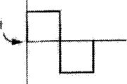
The present invention is easy to be applicable in the additive method that reads magnetic memory device.For example, bipolar pulse can put on reference layer orientation conductor (for example the 3rd conductor 22), and checks the transformation of junction resistance.Fig. 6 A and 7A are illustrated in the illustrated embodiment of variation of the M2 orientation of the pulse signal among corresponding diagram 6B and the 7B.Fig. 6 C and 7C represent the resistance variations or the transformation that obtain.The magnetization orientation of the direction that changes (for example from high to low or from low to high) designation data layer promptly is stored in the logical value in the magnetic memory device.Bipolar read operation is with reference to itself.Therefore, this dynamic readout scheme is insensitive to the difference of different components.
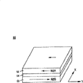
With reference now to Fig. 5,, this figure illustrates magnetic RAM (MRAM) device 610 of a signal embodiment of memory device of the present invention.MRAM device 610 comprises the array 612 of magnetic tunnel-junction (for example magnetic tunnel-junction 11).Magnetic tunnel-junction is arranged in rows and columns, and row extends along the y direction, and row extend along the x direction.Be simple declaration MRAM device 610, only show the magnetic tunnel-junction of relatively small amount.In fact, can adopt the array of virtually any size.The magnetic storage tunnel junction is positioned at the position, point of crossing of two electric conductors (for example word line and bit line).Extend along the x direction as in the plane of conducting element (for example first conductor 18) on array 612 1 sides (for example top side) of word line.Word line contacts with the data Layer (for example data Layer 12) of magnetic tunnel-junction (for example magnetic tunnel-junction 11).As extending along the y direction in the plane of conducting element (for example second conductor 20) on the sides adjacent (for example bottom side) of array 612 of living line.Bit line contacts with the reference layer of magnetic tunnel-junction.In one example, every row of array 612 has a word line, array 612 whenever show a bit line.
Also extend as the conducting element of reading line along a direction (for example y direction).Reading line can be than bit line further from tunnel junction, and can insulate with bit line.MRAM device 610 also comprises the first and second row decoder 614a and 614b, the first and second column decoder 616a and 616b and read/write circuit 618.Read/write circuit 618 comprises sensor amplifier 620, ground wire 622, line current source 624, voltage source 626 and row current source 628.In one embodiment, same electric conductor can be used as and reads and/or write line.
During carrying out write operation on the selected magnetic tunnel-junction (for example magnetic tunnel-junction 11), the first row decoder 614a is connected to line current source 624 with an end of selected word line (for example first conductor 18), the second row decoder 614b is connected to ground with the other end of selected word line, the first column decoder 616a is connected to ground with an end of selected bit line (for example second conductor 20), and secondary series demoder 616b is connected to row current source 628 with the other end of selected bit line.The result is, write current flows through selected word line and bit line (for example 18 and 20).Write current produces magnetic field, and the magnetic moment that makes data and/or reference layer is in the specific direction orientation and influence magnetic tunnel-junction.Column decoder 616a and 616b also can make write current flow through with selected magnetic tunnel-junction intersects and read line (for example conductor 22).This 3rd " writing " electric current produces additional magnetic field, plays booster action when the orientation of the conversion magnetic moment relevant with selected magnetic tunnel-junction.The easy magnetizing axis of data Layer can be in y direction orientation, and correspondingly the data Layer magnetic vector is orientated in the y direction.
During carrying out read operation on the selected magnetic tunnel-junction, the reference that the first and second column decoder 616a and 616b can make steady current flow through and intersect with selected magnetic tunnel-junction (for example magnetic tunnel-junction 11) is orientated line.Produce magnetic field with reference to the orientation electric current, make the magnetization vector of reference layer or vector (for example M2A and M2B) be parallel to word line (for example first conductor 18) orientation.When still applying with reference to the orientation electric current, the first row decoder 614a is connected to selected word line (for example conductor 18) with voltage source 626, and the first column decoder 616a is connected to selected bit line (for example conductor 20) input end virtually of sensor amplifier 620.The result is that read current flows through selected magnetic tunnel-junction (for example magnetic tunnel-junction 11) and arrives the input end of sensor amplifier 620.In this way, can determine the resistance of selected magnetic tunnel-junction.Yet, the invention is not restricted to the method for the resistance of this definite magnetic tunnel-junction.
The present invention is easy to be applicable to the optional coating of using (cladding) on conductor.Coating provides the bigger shielding of adjacent elements, for example, by coating the reference line ferromagnetic material on what its line in office, can make reference line and word line, bit line and/or read the line combination.In a signal embodiment, the combination of reference line and other line is beneficial to be eliminated extra interconnection layer and reduces power consumption, and this is to allow the read and write current amplitude to reduce because coat.
Though explanatory note of the present invention is with reference to tunnel magnetoresistance device (TMR), the present invention must be limited to such magnetic memory device.The present invention can be relevant with the magnetoresistance device of other type with same operation characteristic and implements.For example, the present invention is applicable to gmr (GMR)) device.The GMR device has the basic structure identical with the TMR device, except data Layer and reference layer by conduction nonmagnetic layer rather than tunnel barrier layer separately.Signal layer metal comprises gold, silver and copper.The relative orientation of data and reference magnetization vector influences the interior resistance of face of GMR device.Perhaps, the present invention goes for top and bottom spin value.
Like this, in order to describe and to illustrate, the front provides the explanation of specific embodiments of the present invention.They are not tending towards discharging or limiting the invention to disclosed precise forms, and can make a lot of modifications and change obviously in view of above-mentioned instruction.Select and described embodiment in order to explain principle of the present invention and practical application thereof best, those of ordinary skills can utilize the present invention well thus, and various modification is applicable to the special applications of hope.Therefore scope of the present invention is limited by appended claims and equivalents thereof.
Claims (10)
1. magnetic memory device comprises:
Synthetic ferromagnetic data layer with the magnetic moment (M1) that can point to first orientation and second orientation
(12);
Have the coercitive soft reference layer (14) lower than described synthetic ferromagnetic data layer (12); With
Tunnel layer (16), its resistance characteristic are subjected to the influence of magnetic moment (M1 and the M2) orientation of described synthetic ferromagnetic data layer (12) and described soft reference layer (14).
2. according to the magnetic memory device of claim 1, wherein in described soft reference layer (14), comprise ferromagnetic material.
3. according to the magnetic memory device of claim 1, wherein said soft reference layer (14) is soft synthetic ferromagnetic reference layer.
4. according to the magnetic memory device of claim 3, wherein said synthetic ferromagnetic data layer (12) and described soft synthetic ferromagnetic reference layer (14) respectively comprise:
Have and can be rotated to described first or first sublayer (52) of magnetic moment orientation (M2A) of described second orientation;
Second sublayer (50) with basic maintenance magnetic moment orientation (M2B) opposite with described first sublayer (52); With
The spacer sublayer of described first sublayer of magnetic couplings (52) and described second sublayer (50)
(54)。
5. according to the magnetic memory device of claim 4, it is zero clean coercive force that wherein said soft synthetic ferromagnetic reference layer (14) has.
6. according to the magnetic memory device of claim 4, wherein said data are synthesized ferromagnetic layer (12) and are had greater than the described soft clean coercive force that synthesizes ferromagnetic reference layer (14).
7. according to the magnetic memory device of claim 4, wherein said first sublayer (52) has different structures with described second sublayer (50) in described synthetic ferromagnetic data layer (12) and described soft synthesizing in the ferromagnetic reference layer (14).
8. according to the magnetic memory device of claim 1, wherein said synthetic ferromagnetic data layer (12) and described soft reference layer (14) are coated.
9. according to the magnetic memory device of claim 1, the magnetic field induction that wherein said first and second magnetic alignings are applied in.
10. according to the magnetic memory device of claim 9, the wherein said intensity that applies magnetic field is the order of magnitude less than 7957.7 amperes per meter.
Applications Claiming Priority (2)
| Application Number | Priority Date | Filing Date | Title |
|---|---|---|---|
| US10/196,877 US6850433B2 (en) | 2002-07-15 | 2002-07-15 | Magnetic memory device and method |
| US10/196877 | 2002-07-15 |
Publications (2)
| Publication Number | Publication Date |
|---|---|
| CN1487524A CN1487524A (en) | 2004-04-07 |
| CN100474440C true CN100474440C (en) | 2009-04-01 |
Family
ID=29780188
Family Applications (1)
| Application Number | Title | Priority Date | Filing Date |
|---|---|---|---|
| CNB031360440A Expired - Lifetime CN100474440C (en) | 2002-07-15 | 2003-05-15 | Magnetic memory device and method |
Country Status (5)
| Country | Link |
|---|---|
| US (1) | US6850433B2 (en) |
| EP (1) | EP1383133A1 (en) |
| JP (1) | JP2004064073A (en) |
| CN (1) | CN100474440C (en) |
| TW (1) | TWI308751B (en) |
Families Citing this family (27)
| Publication number | Priority date | Publication date | Assignee | Title |
|---|---|---|---|---|
| JP3788964B2 (en) * | 2002-09-10 | 2006-06-21 | 株式会社東芝 | Magnetic random access memory |
| JP2004165451A (en) * | 2002-11-13 | 2004-06-10 | Sony Corp | Magnetic storage element and its recording method |
| US6944053B2 (en) * | 2003-06-17 | 2005-09-13 | Hewlett-Packard Development Company, L.P. | Magnetic memory with structure providing reduced coercivity |
| US7145795B2 (en) | 2004-04-13 | 2006-12-05 | Micron Technology, Inc. | Multi-cell resistive memory array architecture with select transistor |
| US20070191736A1 (en) * | 2005-10-04 | 2007-08-16 | Don Alden | Method for loading penetrating members in a collection device |
| KR100809724B1 (en) * | 2007-03-02 | 2008-03-06 | 삼성전자주식회사 | Bipolar switching type nonvolatile memory device having tunneling layer |
| US8659852B2 (en) | 2008-04-21 | 2014-02-25 | Seagate Technology Llc | Write-once magentic junction memory array |
| US7855911B2 (en) * | 2008-05-23 | 2010-12-21 | Seagate Technology Llc | Reconfigurable magnetic logic device using spin torque |
| US7852663B2 (en) * | 2008-05-23 | 2010-12-14 | Seagate Technology Llc | Nonvolatile programmable logic gates and adders |
| US7881098B2 (en) | 2008-08-26 | 2011-02-01 | Seagate Technology Llc | Memory with separate read and write paths |
| US7985994B2 (en) | 2008-09-29 | 2011-07-26 | Seagate Technology Llc | Flux-closed STRAM with electronically reflective insulative spacer |
| US8169810B2 (en) | 2008-10-08 | 2012-05-01 | Seagate Technology Llc | Magnetic memory with asymmetric energy barrier |
| US7880209B2 (en) * | 2008-10-09 | 2011-02-01 | Seagate Technology Llc | MRAM cells including coupled free ferromagnetic layers for stabilization |
| US8039913B2 (en) * | 2008-10-09 | 2011-10-18 | Seagate Technology Llc | Magnetic stack with laminated layer |
| US8089132B2 (en) * | 2008-10-09 | 2012-01-03 | Seagate Technology Llc | Magnetic memory with phonon glass electron crystal material |
| US20100102405A1 (en) * | 2008-10-27 | 2010-04-29 | Seagate Technology Llc | St-ram employing a spin filter |
| US8045366B2 (en) | 2008-11-05 | 2011-10-25 | Seagate Technology Llc | STRAM with composite free magnetic element |
| US8043732B2 (en) | 2008-11-11 | 2011-10-25 | Seagate Technology Llc | Memory cell with radial barrier |
| US7826181B2 (en) * | 2008-11-12 | 2010-11-02 | Seagate Technology Llc | Magnetic memory with porous non-conductive current confinement layer |
| US8289756B2 (en) | 2008-11-25 | 2012-10-16 | Seagate Technology Llc | Non volatile memory including stabilizing structures |
| US8037235B2 (en) * | 2008-12-18 | 2011-10-11 | Mosaid Technologies Incorporated | Device and method for transferring data to a non-volatile memory device |
| US7826259B2 (en) | 2009-01-29 | 2010-11-02 | Seagate Technology Llc | Staggered STRAM cell |
| US7999338B2 (en) | 2009-07-13 | 2011-08-16 | Seagate Technology Llc | Magnetic stack having reference layers with orthogonal magnetization orientation directions |
| JP5526707B2 (en) * | 2009-10-27 | 2014-06-18 | ソニー株式会社 | Driving method of information storage element |
| EP2575135B1 (en) * | 2011-09-28 | 2015-08-05 | Crocus Technology S.A. | Magnetic random access memory (MRAM) cell and method for reading the MRAM cell using a self-referenced read operation |
| US9583696B2 (en) | 2014-03-12 | 2017-02-28 | Qualcomm Incorporated | Reference layer for perpendicular magnetic anisotropy magnetic tunnel junction |
| US9825217B1 (en) * | 2016-05-18 | 2017-11-21 | Samsung Electronics Co., Ltd. | Magnetic memory device having cobalt-iron-beryllium magnetic layers |
Family Cites Families (14)
| Publication number | Priority date | Publication date | Assignee | Title |
|---|---|---|---|---|
| US5465185A (en) * | 1993-10-15 | 1995-11-07 | International Business Machines Corporation | Magnetoresistive spin valve sensor with improved pinned ferromagnetic layer and magnetic recording system using the sensor |
| JP3691898B2 (en) * | 1996-03-18 | 2005-09-07 | 株式会社東芝 | Magnetoresistive effect element, magnetic information reading method, and recording element |
| JP3957817B2 (en) * | 1997-06-12 | 2007-08-15 | キヤノン株式会社 | Magnetic thin film memory and recording / reproducing method thereof |
| US5936293A (en) * | 1998-01-23 | 1999-08-10 | International Business Machines Corporation | Hard/soft magnetic tunnel junction device with stable hard ferromagnetic layer |
| US5953248A (en) * | 1998-07-20 | 1999-09-14 | Motorola, Inc. | Low switching field magnetic tunneling junction for high density arrays |
| US6165803A (en) * | 1999-05-17 | 2000-12-26 | Motorola, Inc. | Magnetic random access memory and fabricating method thereof |
| US6436526B1 (en) * | 1999-06-17 | 2002-08-20 | Matsushita Electric Industrial Co., Ltd. | Magneto-resistance effect element, magneto-resistance effect memory cell, MRAM and method for performing information write to or read from the magneto-resistance effect memory cell |
| US6166948A (en) | 1999-09-03 | 2000-12-26 | International Business Machines Corporation | Magnetic memory array with magnetic tunnel junction memory cells having flux-closed free layers |
| JP2001196658A (en) * | 2000-01-07 | 2001-07-19 | Fujitsu Ltd | Magnetic element and magnetic memory device |
| JP2002074937A (en) * | 2000-09-01 | 2002-03-15 | Canon Inc | Magnetic thin-film memory and method of manufacturing the same |
| US6795281B2 (en) * | 2001-09-25 | 2004-09-21 | Hewlett-Packard Development Company, L.P. | Magneto-resistive device including soft synthetic ferrimagnet reference layer |
| US6576969B2 (en) * | 2001-09-25 | 2003-06-10 | Hewlett-Packard Development Company, L.P. | Magneto-resistive device having soft reference layer |
| US6538917B1 (en) * | 2001-09-25 | 2003-03-25 | Hewlett-Packard Development Company, L.P. | Read methods for magneto-resistive device having soft reference layer |
| US6593608B1 (en) * | 2002-03-15 | 2003-07-15 | Hewlett-Packard Development Company, L.P. | Magneto resistive storage device having double tunnel junction |
-
2002
- 2002-07-15 US US10/196,877 patent/US6850433B2/en not_active Expired - Lifetime
-
2003
- 2003-03-04 TW TW092104568A patent/TWI308751B/en not_active IP Right Cessation
- 2003-05-15 CN CNB031360440A patent/CN100474440C/en not_active Expired - Lifetime
- 2003-05-16 EP EP03253082A patent/EP1383133A1/en not_active Withdrawn
- 2003-06-30 JP JP2003186790A patent/JP2004064073A/en active Pending
Also Published As
| Publication number | Publication date |
|---|---|
| US6850433B2 (en) | 2005-02-01 |
| TWI308751B (en) | 2009-04-11 |
| US20040008537A1 (en) | 2004-01-15 |
| JP2004064073A (en) | 2004-02-26 |
| EP1383133A1 (en) | 2004-01-21 |
| TW200401290A (en) | 2004-01-16 |
| CN1487524A (en) | 2004-04-07 |
Similar Documents
| Publication | Publication Date | Title |
|---|---|---|
| CN100474440C (en) | Magnetic memory device and method | |
| JP4658102B2 (en) | Readout method for a magnetoresistive element having a magnetically soft reference layer | |
| CN100447892C (en) | Magnetic storage device with soft reference layer | |
| US6404674B1 (en) | Cladded read-write conductor for a pinned-on-the-fly soft reference layer | |
| US6538920B2 (en) | Cladded read conductor for a pinned-on-the-fly soft reference layer | |
| US6593608B1 (en) | Magneto resistive storage device having double tunnel junction | |
| CN100576344C (en) | Be used for the synthetic-ferrimagnet sensing layer that high density mram is used | |
| US6891746B2 (en) | Magneto-resistive device having soft reference layer | |
| EP0613148A2 (en) | Nonvolatile magnetoresistive storage device | |
| US6504221B1 (en) | Magneto-resistive device including soft reference layer having embedded conductors | |
| US6735112B2 (en) | Magneto-resistive memory cell structures with improved selectivity | |
| US6795281B2 (en) | Magneto-resistive device including soft synthetic ferrimagnet reference layer | |
| JP4477829B2 (en) | Method of operating a magnetic storage device | |
| JP2003197872A (en) | Memory using magneto-resistance effect film |
Legal Events
| Date | Code | Title | Description |
|---|---|---|---|
| C06 | Publication | ||
| PB01 | Publication | ||
| C10 | Entry into substantive examination | ||
| SE01 | Entry into force of request for substantive examination | ||
| ASS | Succession or assignment of patent right |
Owner name: SAMSUNG ELECTRONICS CO., LTD Free format text: FORMER OWNER: HEWLETT-PACKARAD DEVELOPMENT INC. Effective date: 20071228 |
|
| C41 | Transfer of patent application or patent right or utility model | ||
| TA01 | Transfer of patent application right |
Effective date of registration: 20071228 Address after: Gyeonggi Do, South Korea Applicant after: SAMSUNG ELECTRONICS Co.,Ltd. Address before: Texas, USA Applicant before: Hewlett-Packard Development Co.,L.P. |
|
| C14 | Grant of patent or utility model | ||
| GR01 | Patent grant | ||
| CX01 | Expiry of patent term |
Granted publication date: 20090401 |
|
| CX01 | Expiry of patent term |