CN100476586C - Transmission shear grating in checkerboard configuration for EUV wavefront sensor - Google Patents
Transmission shear grating in checkerboard configuration for EUV wavefront sensor Download PDFInfo
- Publication number
- CN100476586C CN100476586C CNB2004100019184A CN200410001918A CN100476586C CN 100476586 C CN100476586 C CN 100476586C CN B2004100019184 A CNB2004100019184 A CN B2004100019184A CN 200410001918 A CN200410001918 A CN 200410001918A CN 100476586 C CN100476586 C CN 100476586C
- Authority
- CN
- China
- Prior art keywords
- grating
- electromagnetic radiation
- projection optics
- focal plane
- detecting device
- Prior art date
- Legal status (The legal status is an assumption and is not a legal conclusion. Google has not performed a legal analysis and makes no representation as to the accuracy of the status listed.)
- Expired - Fee Related
Links
- 230000005540 biological transmission Effects 0.000 title claims description 16
- 230000005670 electromagnetic radiation Effects 0.000 claims abstract description 21
- 230000003287 optical effect Effects 0.000 claims abstract description 17
- 238000003384 imaging method Methods 0.000 claims abstract description 10
- 210000001747 pupil Anatomy 0.000 claims abstract description 8
- 238000010008 shearing Methods 0.000 claims abstract description 5
- 238000000034 method Methods 0.000 claims description 17
- XUIMIQQOPSSXEZ-UHFFFAOYSA-N Silicon Chemical compound [Si] XUIMIQQOPSSXEZ-UHFFFAOYSA-N 0.000 claims description 13
- 229910052710 silicon Inorganic materials 0.000 claims description 13
- 239000010703 silicon Substances 0.000 claims description 13
- 239000000758 substrate Substances 0.000 claims description 8
- PXHVJJICTQNCMI-UHFFFAOYSA-N Nickel Chemical compound [Ni] PXHVJJICTQNCMI-UHFFFAOYSA-N 0.000 claims description 6
- 229910052751 metal Inorganic materials 0.000 claims description 4
- 239000002184 metal Substances 0.000 claims description 4
- 235000009508 confectionery Nutrition 0.000 claims description 3
- 230000001788 irregular Effects 0.000 claims description 3
- 229910052759 nickel Inorganic materials 0.000 claims description 3
- 238000002310 reflectometry Methods 0.000 claims description 3
- 230000001105 regulatory effect Effects 0.000 claims description 2
- 238000010521 absorption reaction Methods 0.000 claims 5
- 150000004767 nitrides Chemical class 0.000 claims 3
- 230000003321 amplification Effects 0.000 claims 2
- 238000003199 nucleic acid amplification method Methods 0.000 claims 2
- 239000010453 quartz Substances 0.000 claims 2
- VYPSYNLAJGMNEJ-UHFFFAOYSA-N silicon dioxide Inorganic materials O=[Si]=O VYPSYNLAJGMNEJ-UHFFFAOYSA-N 0.000 claims 2
- 238000005259 measurement Methods 0.000 abstract description 4
- 230000004075 alteration Effects 0.000 abstract description 2
- 230000010363 phase shift Effects 0.000 abstract 1
- 230000005855 radiation Effects 0.000 abstract 1
- 238000005530 etching Methods 0.000 description 6
- 238000004519 manufacturing process Methods 0.000 description 4
- 239000004065 semiconductor Substances 0.000 description 4
- 230000004888 barrier function Effects 0.000 description 3
- 230000007423 decrease Effects 0.000 description 3
- 238000010586 diagram Methods 0.000 description 3
- 239000002994 raw material Substances 0.000 description 3
- 238000004458 analytical method Methods 0.000 description 2
- 239000011521 glass Substances 0.000 description 2
- 238000005286 illumination Methods 0.000 description 2
- VYZAMTAEIAYCRO-UHFFFAOYSA-N Chromium Chemical compound [Cr] VYZAMTAEIAYCRO-UHFFFAOYSA-N 0.000 description 1
- 229910052581 Si3N4 Inorganic materials 0.000 description 1
- 230000008033 biological extinction Effects 0.000 description 1
- 238000004364 calculation method Methods 0.000 description 1
- 229910052804 chromium Inorganic materials 0.000 description 1
- 239000011651 chromium Substances 0.000 description 1
- 230000001427 coherent effect Effects 0.000 description 1
- 238000001514 detection method Methods 0.000 description 1
- 230000008034 disappearance Effects 0.000 description 1
- 230000008030 elimination Effects 0.000 description 1
- 238000003379 elimination reaction Methods 0.000 description 1
- 238000005516 engineering process Methods 0.000 description 1
- 239000000463 material Substances 0.000 description 1
- 239000011159 matrix material Substances 0.000 description 1
- 238000012856 packing Methods 0.000 description 1
- 238000012857 repacking Methods 0.000 description 1
- 238000000926 separation method Methods 0.000 description 1
- HQVNEWCFYHHQES-UHFFFAOYSA-N silicon nitride Chemical compound N12[Si]34N5[Si]62N3[Si]51N64 HQVNEWCFYHHQES-UHFFFAOYSA-N 0.000 description 1
Images


Classifications
-
- G—PHYSICS
- G03—PHOTOGRAPHY; CINEMATOGRAPHY; ANALOGOUS TECHNIQUES USING WAVES OTHER THAN OPTICAL WAVES; ELECTROGRAPHY; HOLOGRAPHY
- G03F—PHOTOMECHANICAL PRODUCTION OF TEXTURED OR PATTERNED SURFACES, e.g. FOR PRINTING, FOR PROCESSING OF SEMICONDUCTOR DEVICES; MATERIALS THEREFOR; ORIGINALS THEREFOR; APPARATUS SPECIALLY ADAPTED THEREFOR
- G03F7/00—Photomechanical, e.g. photolithographic, production of textured or patterned surfaces, e.g. printing surfaces; Materials therefor, e.g. comprising photoresists; Apparatus specially adapted therefor
- G03F7/70—Microphotolithographic exposure; Apparatus therefor
- G03F7/708—Construction of apparatus, e.g. environment aspects, hygiene aspects or materials
- G03F7/7085—Detection arrangement, e.g. detectors of apparatus alignment possibly mounted on wafers, exposure dose, photo-cleaning flux, stray light, thermal load
-
- G—PHYSICS
- G01—MEASURING; TESTING
- G01J—MEASUREMENT OF INTENSITY, VELOCITY, SPECTRAL CONTENT, POLARISATION, PHASE OR PULSE CHARACTERISTICS OF INFRARED, VISIBLE OR ULTRAVIOLET LIGHT; COLORIMETRY; RADIATION PYROMETRY
- G01J9/00—Measuring optical phase difference; Determining degree of coherence; Measuring optical wavelength
- G01J9/02—Measuring optical phase difference; Determining degree of coherence; Measuring optical wavelength by interferometric methods
- G01J9/0215—Measuring optical phase difference; Determining degree of coherence; Measuring optical wavelength by interferometric methods by shearing interferometric methods
-
- G—PHYSICS
- G02—OPTICS
- G02B—OPTICAL ELEMENTS, SYSTEMS OR APPARATUS
- G02B5/00—Optical elements other than lenses
- G02B5/18—Diffraction gratings
- G02B5/1838—Diffraction gratings for use with ultraviolet radiation or X-rays
-
- G—PHYSICS
- G03—PHOTOGRAPHY; CINEMATOGRAPHY; ANALOGOUS TECHNIQUES USING WAVES OTHER THAN OPTICAL WAVES; ELECTROGRAPHY; HOLOGRAPHY
- G03F—PHOTOMECHANICAL PRODUCTION OF TEXTURED OR PATTERNED SURFACES, e.g. FOR PRINTING, FOR PROCESSING OF SEMICONDUCTOR DEVICES; MATERIALS THEREFOR; ORIGINALS THEREFOR; APPARATUS SPECIALLY ADAPTED THEREFOR
- G03F7/00—Photomechanical, e.g. photolithographic, production of textured or patterned surfaces, e.g. printing surfaces; Materials therefor, e.g. comprising photoresists; Apparatus specially adapted therefor
- G03F7/70—Microphotolithographic exposure; Apparatus therefor
- G03F7/70483—Information management; Active and passive control; Testing; Wafer monitoring, e.g. pattern monitoring
- G03F7/70591—Testing optical components
- G03F7/706—Aberration measurement
-
- H—ELECTRICITY
- H01—ELECTRIC ELEMENTS
- H01L—SEMICONDUCTOR DEVICES NOT COVERED BY CLASS H10
- H01L22/00—Testing or measuring during manufacture or treatment; Reliability measurements, i.e. testing of parts without further processing to modify the parts as such; Structural arrangements therefor
- H01L22/10—Measuring as part of the manufacturing process
- H01L22/12—Measuring as part of the manufacturing process for structural parameters, e.g. thickness, line width, refractive index, temperature, warp, bond strength, defects, optical inspection, electrical measurement of structural dimensions, metallurgic measurement of diffusions
-
- G—PHYSICS
- G01—MEASURING; TESTING
- G01J—MEASUREMENT OF INTENSITY, VELOCITY, SPECTRAL CONTENT, POLARISATION, PHASE OR PULSE CHARACTERISTICS OF INFRARED, VISIBLE OR ULTRAVIOLET LIGHT; COLORIMETRY; RADIATION PYROMETRY
- G01J9/00—Measuring optical phase difference; Determining degree of coherence; Measuring optical wavelength
- G01J9/02—Measuring optical phase difference; Determining degree of coherence; Measuring optical wavelength by interferometric methods
- G01J9/0215—Measuring optical phase difference; Determining degree of coherence; Measuring optical wavelength by interferometric methods by shearing interferometric methods
- G01J2009/0219—Measuring optical phase difference; Determining degree of coherence; Measuring optical wavelength by interferometric methods by shearing interferometric methods using two or more gratings
Abstract
A wavefront measurement system includes a source of electromagnetic radiation. An imaging system directs the electromagnetic radiation at an object plane that it uniformly illuminates. A first grating is positioned in the object plane to condition the radiation entering the input of a projection optic. A projection optical system projects an image of the first grating onto the focal plane. A second grating is positioned at the focal plane that receives a diffracted image of the object plane to form a shearing interferometer. A CCD detector receives the image of the pupil of the projection optical system through the projection optical system and the second grating that forms a fringe pattern if there are aberrations in the projection optical system. Phaseshift readout of fringe pattern can be accomplished by stepping the first grating in a lateral direction and reading each frame with the CCD detector.
Description
Technical field
The present invention relates generally to extreme ultraviolet light (EUV) etch system, relate in particular in a photoetch system measurement wave front (wavefront) parameter.
Background technology
Etching is the process that is used for forming pattern on substrate surface.This type of substrate comprises those employed substrates in the manufacture process of panel display screen, circuit board and various integrated circuit etc.Normally used substrate is a slice semiconductor wafer in this class is used.Be familiar with correlation technique and can find out that the description here also is applicable to the substrate of other types.
In etching process, place an exposure system within the etch system piece image to be projected on the surface of a wafer, this wafer is placed on the wafer station (WS).Described exposure system comprises that one is used for the graticule (reticle) (also claim light barrier) of image projection to the wafer.
Described graticule is installed on the graticule platform (RS), between semi-conductor chip and light source usually.In the photoetch process, this graticule is used as a light barrier, is used for printed circuit on semi-conductor chip.Etching light is by described light barrier, then again through a series of optical lenses that are used for downscaled images.Then, this little image is projected onto on silicon wafer or the semiconductor wafer.This process and camera make light imaging process on egative film similar.In the photoetch process, light plays a part very important.For instance, in the manufacture process of microprocessor (being computer chip), the key of producing microprocessor with better function is the wavelength of used light.Wavelength is short more, just can be on silicon wafer the more transistor of etching.And if on the silicon wafer a large amount of transistors are arranged, its function is just more powerful, and speed is just fast more.
Because manufacturers can use more short wavelength's light, they have also just run into the problem that glass lens absorbed that short wavelength light more is used for optically focused originally.More short wavelength light also just can't arrive on the silicon wafer owing to be absorbed.As a result, on silicon wafer, just there is not the generative circuit pattern yet.For attempting overcoming this problem, chip manufacturers have developed an etching process that is called extreme ultraviolet photoetch (EUVL).In this process, can replace a glass lens with a catoptron.
In described etching process, the problem of measuring the illumination beam quality exists all the time.Especially, wave front produce and exposure process in, we wish and can measure the wave front quality in the photoetch tool interior, and needn't dismantle this instrument for this reason.An EUV instrument is wasted time and energy to feasible dismounting of the demand of specific environment.
Summary of the invention
The present invention mainly is a projection shear grating (transmission sheargrating) and a checkerboard type setting, is used for an EUV wavefront sensor that can fully overcome the one or more problems and the shortcoming of correlation technique.
One embodiment of the invention comprise a wave front measuring system, and this system comprises an electromagnetic radiation source; An imaging system is used for described electromagnetic radiation evenly is mapped to an object plane; Be positioned at first grating of object plane, be used for regulating the irradiates light on the incident NA unthreaded hole plane that arrives projection optics system (PO), first grating comprises the reflected ray that many each free a plurality of reflection spots constitute; A projection optics system is used for a picture of described first grating is projected the focal plane; Be positioned at second grating of described focal plane; A detector that is positioned at fringe plane is used for receiving a plurality of pictures by the described PO unthreaded hole of second grating.
Will illustrate further feature of the present invention and advantage in the following description, these features and advantage can partly obviously be found out from describe, or learn by putting into practice the present invention.Advantage of the present invention will realize and obtain, and point out in text description, related right claim and accompanying drawing especially by described structure.
Should be understood that the generality of front is described and following detailed all is exemplary, illustrative, be used for that the present invention is further illustrated.
Description of drawings
Accompanying drawing is introduced into to describe illustrative embodiments of the present invention and to be merged to constitute the part of this explanation, be used for describing the embodiments of the present invention and and text description together be used to explain principle of the present invention.In the accompanying drawings:
Fig. 1 shows the part of an EUV photoetch system.
It is the described photoetch system of how packing into that Fig. 2 shows a sensor assembly of the present invention and light source module.
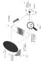
Fig. 3 shows the example of a 2-D checkerboard type grating.
Fig. 4 and Fig. 5 have described the process that produces the shear wave front with an interferometer.
Fig. 6 is another synoptic diagram when the present invention is used in the photoetch instrument.
Fig. 7-11 has described the example of the interference fringe of seeing in the focal plane when application is of the present invention.
Figure 12 has described an embodiment that uses the source module grating of random pattern reflection spot.
Embodiment
Describe the embodiments of the present invention now in detail, the example is described in the drawings.
Fig. 1 has described the part of an EUV photoetch system 100, comprises an EUV light source (not shown in figure 1).This system 100 also comprises imaging optical system (comprising mirror M 4 and M3), and 101, one of a unthreaded hole places graticule platform (RS, not shown) on graticule 102, the picture of pattern will project on the wafer 105, and projection system (PO) 104, mirror M 1 and M4.Then, the extreme ultraviolet ray is projected onto on the wafer 105 that places on the wafer station (WS, not shown).Should see that described graticule 102 reflects in the EUV system, and in the photoetch system under working in long wavelength more, such as under deep UV (ultraviolet light) or the visible wavelength, the normally transmission of this graticule 102.
As further illustrating among Fig. 1, in the present invention, a sensor assembly 106 places on the described wafer station, and a light source module 103 places on the described graticule platform, is used to measure wave front.Described sensor and light source module 106 also can be called a wavefront sensor (WFS).
Fig. 2 is another diagram of described wavefront measuring apparatus of the present invention, can integrate with in the photoetch system particularly in it.As may seeing among Fig. 2, light source module 103 places on the described graticule platform, comprises the grating that two quadratures are placed in one embodiment.Described wavefront sensor (or sensor assembly 106) places on the described wafer station and comprises a 2-D grating 102 and ccd detector 202 that one is positioned at this 2-D grating below.Described projection optics system (PO) 104 carries out normal exposing operation as before.
Described wave front can not measured when carrying out imaging.For measuring wave front, described graticule platform is moved, and one in the grating 203 on the described graticule platform in the light source module 103 is placed in the light path, rather than graticule 102 is own.Described wafer station also is moved, thereby described wavefront sensor is placed a picture that receives described light source module grating 203.Then, the ccd detector under the described 2-D grating 201 202 just receives and measures transmitted ray.Described then graticule platform just is moved with different diffraction grating of placement in light path, thereby measures described wave front with an orthogonal directions of light source module grating 203.
Fig. 3 has described an embodiment of 2-D grating 201 of the present invention.As shown in Figure 3, can use the checkerboard type grating of a spacing through carefully choosing.Such grating can be made in the substrate of for example 100 nanometer thickness, and its raw material is transmission under described exposure wavelength.For instance, the example of this class transmission raw material comprises silicon and silicon nitride under 13.5 nano wave lengths.Like this, described 2-D checkerboard type diffraction grating 201 just we can say to have 50% dutycycle.Elementary interference will be that zeroth order and positive and negative single order are interfered.The randomness that is derived from the diffuse scattering of light source module 103 will be as expecting that elimination is by the spatial variations in the wave front of the unthreaded hole of projection system 104 effectively.It should be noted that as can seeing among Fig. 3, the spacing of 2-D grating 201 is vertical foursquare length.
Described 2-D grating 201 also comprises reflection (or opaque) zone, as can seeing among Fig. 3.These reflector spaces can be made of the material that absorbs EUV light (in this case, being 13.5 nanometer exposure wavelengths), such as nickel, chromium or other metal.
In one embodiment, described checkerboard type grating space is chosen to be 1.6 microns.Should notice that described spacing must careful select, thereby be that a specific shear rate (shear ratio) and numerical aperture are that (as following discussion) suitable angle of generation is interfered on first rank.In a first-selected embodiment, described shear rate is chosen as 1/30
Th, and those skilled in the art should see and the invention is not restricted to these optional network specific digits or size.In addition, in a specific implementations, the Launch numerical aperture that goes out of described system is 0.25 (going into Launch numerical aperture is 0.0625, and enlargement ratio is 4X), and the present invention is not limited to this specific numerical aperture.
As mentioned above, the spacing of described in one embodiment 2-D grating 201 is used to provide one 1/30
ThShear rate, wherein said ccd detector 202 is the perhaps multiple folded ring of light of " a seeing " candy strip (interferogram) in described fringe plane (such as, below the focal plane of described system), as following will further the discussion.Described shear rate (shear ratio) is that to the overlapping of two rings of light measures, wherein shear rate be zero represented complete overlapping.It shall yet further be noted that we wish 202 " seeing " zeroth orders of ccd detector and positive and negative single order diffraction image, and eliminate the positive and negative second order of diffraction image.For this reason, as shown in Figure 3, use a checkerboard type grating to believe it is best with square projection and reflector space.In addition, described first grating 103 is configured and helps eliminate the diffraction exponent number of not wishing to get.Yet, no matter using the projection and the reflector space of what pattern, importantly described 2-D grating is made of regular pattern.Should see that as long as described pattern is regular, then other shape outside the square also is possible, such as circular reflector space or circular projected area.
Those skilled in the art also can appreciate the part tolerance (tolerancing) that relates between sensor assembly 106 and the light source module 103 and can solve by following steps: the 2-D grating 201 of making described sensor assembly 106 earlier, measure its accurate size, correspondingly make described light source module grating 203 then.In a 4X enlargement ratio system, the spacing of the striated pattern of light source module 103 preferably be exactly sensor assembly 106 2-D grating 201 4X doubly.Like this, if the spacing of 2-D grating 201 is 1.6 microns, then the spacing of light source module grating 203 is just preferably 6.4 microns.Yet, if 2-D grating 201 is recorded with its nominal value 1.6 for example 10% deviation being arranged, light source module grating 203 just can manufacture in view of the above has 4X doubly to the spacing of survey checkerboard type grating space.This has just reduced in the manufacture process of two cover gratings simultaneously to its extremely requirement of accuracy.
Another embodiment of described 2-D grating 201 is a crossed grating, make one in two striated patterns with a suitable spacing to place on another so in fact, and wherein each grating all have suitable spacing dimension to obtain a suitable combination diagonal line spacing.Yet, believe that described checkerboard type grating can provide optimal results.
Should see that also the striated pattern that checkerboard type grating or crossed grating can replace two separation is applied in the described light source module 103, though use a 2-D grating can make reading of detector and analytical calculation more complicated in light source module 103.
Also should see, although top discussion mainly is about an EUV photoetch system, its characteristic feature is that the use of reflective optical devices is (such as light source module grating 203, projection optics system 104 and imaging system), when substituting reflection subassembly with suitable transmitted/refracted assembly, the present invention is equally applicable to employed other wavelength light in described photoetch system.
The spacing of described light source module grating 204 also can chosenly make the interference between the positive and negative single order image disappear.
Fig. 4 and Fig. 5 have described in a horizontal shearing interferometer (lateral shearinterferometer) use to a unthreaded hole, to produce reference wave front and shear wave front.(also seeing the entrance pupil 101 among Fig. 1) as shown in Figures 4 and 5, after dispersing from an original light source, wave front 401 in the space some place assemble.A picture of pointolite 402 is present in entrance pupil 101 places.Can place a part printing opacity egative film 415 at entrance pupil 101 places.A pin hole 403 is positioned at entrance pupil 101 places.Wave front of this pin hole generation is 411 transmitted wave 404, comprising a diffraction sphere reference wave 405.Described so horizontal shearing interferometer 410 has just produced one or more pseudo-light sources, and its wave front 411 interferes to produce striped 412.
Fig. 6 is another diagram of described wave front measuring system of the present invention, shows the light source module 103 and the projection system 104 that are positioned at described object plane (graticule 102 planes do not mark among the figure).One places on the described wafer station as shear grating 201, and produces the multiple wave front that is detected as candy strip thereafter in sensor assembly 202.
Fig. 7 has described by ccd detector 202 detected wave front stripeds (412 among Fig. 4).As shown in Figure 7, among the dexter in the above figure, show the shear striped of a single object space slit (single object space slit), wherein this slit is positioned at the place ahead in a non-coherent scattering source, and this light source has filled up maximum numerical aperture and level and smooth any wave front is inhomogeneous.Following right-hand side illustrates the ripple observability function 601 of a zeroth order and single order diffraction pattern.The wave front striped is formed by the zeroth order at PO unthreaded hole place and the interference of positive and negative single order diffraction.50% dutycycle makes that the diffraction pattern of all even-orders is invisible on the described grating 201.Show shear rate in the lower left corner of Fig. 7 and be 0.5 image space shear grating 201.
Fig. 8-11 has described by ccd detector 202 detected exemplary wave fronts by different shear rates.
Further with reference to figure 1 and Figure 10, absorb many picture N at ccd detector 202 places simultaneously and further analyze described wave front by scan described graticule platform with each live width/N.For the grating 203 of one 6.4 micron pitch, and 16 pictures, then described graticule platform is scanned with each 6.4 microns/16=400 nanometer.These pictures can be combined by the principle of phase shifting interferometer to obtain a ratio from a getable better analysis of single picture then.
An ever-present particular problem is in many EUV photoetchs system, the EUV light source can't provide uniform irradiation at the unthreaded hole place of PO, but many plane of polarisations or polarisation point are arranged, this is owing to used fly lens caused in the optical device of EUV light source.This caused the unthreaded hole of PO104 to go into Launch numerical aperture place wave front inhomogeneous, perhaps cause the numerical aperture of underfill PO sometimes.For instance, the particular system of an embodiment of the invention have one be used for described projection optics system 104 go into Launch numerical aperture 0.0625, and output numerical aperture 0.25.Like this, just wish and to eliminate discontented and intensity inequality at the Launch numerical aperture place of going into of PO104.Should notice that problem discussed above can influence the measurement of described wave front by aforementioned wavefront sensor.
Figure 12 has described one and has been used to overcome the solution that these problems propose.As shown in Figure 12, wherein described a class striated pattern, every reflected ray of this grating is not by continuous reflection strip (or line) but is made of a plurality of reflection spots.These reflection spots can be stochastic distribution, as shown in Figure 12, also can arrange by the matrix pattern of a rule.Like this, as from seeing Figure 12, when " from afar " when seeing, the line of the grating 1202 of described light source module seems to be exactly solid line, and is the same as discussed above.Yet, (to describe) when seeing when " from nearby " as 1204 places, they are made of many reflection spots.In EUV uses, remaining raw material will be an extinction.
The same as has been stated, described grid stroke is chosen next directly related with second grid stroke, thereby further utilizes described object plane irradiates light to greatest extent, keeps the striped observability at described detector place, and eliminates positive and negative single order striped.
In one embodiment, corresponding to parameter discussed above (6.4 microns are used for 4X and doubly amplify, and 0.25 goes out Launch numerical aperture, and 0.0625 goes into Launch numerical aperture, 13.5 nanometers light), the diameter of described point is between 70 to 120 nanometers, preferably near 70 nanometers.
The bottom of Figure 12 shows the overall alignment of uniting two quadratures placement gratings that constitute light source module grating 203 of the present invention.As may seeing in Figure 12 bottom, reflection spot can be discharged in two adjacent quadrature patterns, takes advantage of 200 microns for each about 200 microns.
Should appreciate owing to used reflection spot in the present invention, as shown in Figure 10, described single diffraction pattern has become the diffraction pattern within the diffraction pattern.Like this, from the focal plane, each reflection spot all becomes a wave front source.Therefore, intensity is irregular, irregular will the disappearance of intensity that causes by the fly's eye facet of light source (fly ' s eye facets) particularly, and on described focal plane, present the picture of a neat rule of light source.The reflection spot pattern of grating 203 equally also has advantage, and it has been full of 0.0625 numerical aperture of described projection optics system, and the light that incides on the grating 203 that utilized as much as possible.In addition, if the irradiates light at object plane place is a spatial independence, then there are not extra unthreaded hole facet (pupilfacet) or unthreaded hole structure to be introduced into.Reflection spot grating shown in Figure 12 is made on the blank graticule of a standard.Described spot diameter preferably is chosen to be greater than being full of the required value of described numerical aperture, is bordering on uniform unthreaded hole irradiation to provide.
In addition, because the basic detection signal-to-noise ratio of the limited noise of photon only increases according to square root, then can be allowed to the factor be that 2 intensity declines and falls to each point.Should also be noted that for the problem on making and to wish that bigger diameter is arranged.For instance, calculate the point show one 44 nanometer diameter and cause that one 10% decline fall, one 66 nanometer diameter point causes that one 20% decline fall, and one 112 nanometer diameter point causes that then one 50% decline fall.
Like this, reflection spot grating 203 of the present invention is examples of a reflectivity EUV scattering device, and it has 0.4% efficient for a large amount of reflection spots and first raster size in the case, and has the additional object that makes this maximizing efficiency.The definitions of efficiency here is for to compare with lambert's scatterer (Lambertain diffuser), and irradiation power falls into the part in the required numerical aperture after the described device reflection.
A reflection EUV diffractometer of reequiping has been full of the Launch numerical aperture of going into of described projection optics system, eliminating the unthreaded hole facet that causes by illumination subsystem, and utilize to greatest extent described irradiation with under the EUV wavelength with the aberration of a horizontal raster shearing interferometer measurement optical system.Require equivalent with a grating to be placed at before the incoherent expansion light source in the described reticle plane at last.Preceding 2 require the incident irradiates light to be reflected by a diffractometer, and this diffractometer has a pattern that is better than lambert's scatterer.The reflection diffraction device of described repacking can be the integral body with the grating micro-reflector diffraction-limited spot that is form.Independent reflection spot is placed in 50% dutycycle " grating " in this integral body " slit " located and the size of each independent reflection spot and the Launch numerical aperture of going into that shape all can be full of just measured optical system by diffraction.For 0.0625 numerical aperture under 13.5 nano wave lengths, spot diameter should be in 70 nanometers (to 210 nanometers).70 single nano dots can obtain about 0.01 " detectable " EUV photon at EUV ILIAS.Yet, one has 45 stripe pitch is the grating of 6.4 microns the grid stroke and 300 microns long 50% dutycycle of only having a few along the central shaft of every line, can hold enough points to obtain 1,000 " can detect " photon altogether, this has had enough and to spare for EUV ILIAS." grating " line that has been covered with reflection spot can provide bigger signal.Independent (having a few) line can provide an insufficient signal.The regular grating of lambert's scatterer and similar structures can provide a just sufficient signal.
Described reflection spot can have different height so that phase differential to be provided, thus the center bright spot of the random pattern before eliminating.Also serve identical purpose by the random phase that highly causes at random.Yet the spot that is present in the partial coherence irradiation may be a problem concerning some are used.Described reflection spot can be placed under the situation of no phase step regularly, and the placement of such rule may become spot not very low-frequency artificial ripple of trouble so.
When reflection spot was placed in grid stroke at random, spot and center bright spot just appearred in the clause pattern.This center bright spot can add a part and eliminate by making the reflection spot of height at random with the standard variance (that is many times of π of optical path difference) that is multiple times than wavelength.When reflection spot was placed with regular pattern, the overlapping artificial striped in fringe plane can be eliminated (but can generate spot) by making the reflection spot of height at random have the optical path difference that a standard deviation is multiple times than π equally.Yet artificial striped may be less to the influence of fringe analysis.
The person skilled in the art should be appreciated that, under the prerequisite of the spirit of the present invention of defined and scope, can do various changes on form and details in not deviating from as appended claims.Like this, range of the present invention and scope should not be limited to any above-mentioned illustrative embodiments, can only be consistent with following claims and equivalents thereof but should be prescribed.
Claims (61)
1. wave front measuring system comprises:
An electromagnetic radiation source;
An irradiation system is used for described electromagnetic radiation is evenly impinged upon on the object plane;
First grating that is positioned at described object plane is used for regulating described electromagnetic radiation;
A projection optics system is used for a picture of described first grating is projected on the focal plane;
Second grating that is positioned at described focal plane; And
A detecting device that is positioned at after described second grating is used for receiving a candy strip that is produced by described second grating,
Wherein, the reflection, transmission or the refracted ray that be used in described first grating to reflect, transmission or refraction electromagnetic radiation generate diffraction pattern comprise a plurality of points.
2. the system of claim 1, wherein said second grating is a two-dimensional grating.
3. the system of claim 2, wherein said two-dimensional grating is a checkerboard type grating.
4. the system of claim 2, wherein said two-dimensional grating is a crossed grating.
5. power requires 1 system, and wherein said first grating is a reflectivity grating.
6. the system of claim 1, wherein said second grating comprises a regular pattern of absorption region and regional transmission.
7. the system of claim 1, wherein said electromagnetic radiation source is an extreme ultraviolet light (EUV) radiographic source.
8. the system of claim 1, wherein said electromagnetic radiation source is the radiographic source of one 13.5 nanometer.
9. the system of claim 1, wherein said first grating is contained on the graticule platform.
10. the system of claim 1, wherein said second grating is contained on the wafer station.
11. the system of claim 1, wherein said first grating becomes miter angle with respect to described second grating.
12. the system of claim 1, a spacing of wherein said first grating equal the amplification factor that a spacing of described second grating multiply by described projection optics system.
13. the system of claim 1, wherein said first grating is a checkerboard type grating.
14. the system of claim 1, wherein said first grating is a striated pattern.
15. the system of claim 1, also comprise one with the described first grating quadrature and the 3rd grating that can replace described first grating in described object plane, to place.
16. the system of claim 1, wherein said detecting device is a charge-coupled device (CCD) (CCD) detecting device.
17. the system of claim 1, wherein said second grating forms in a slice at nitride silicon based the end.
18. the system of claim 1, wherein said second grating forms on a slice silicon base.
19. the system of claim 1, wherein said first grating forms in a slice at nitride silicon based the end.
20. the system of claim 1, wherein said first grating forms on one of a slice quartz substrate and a slice silicon base.
21. the system of claim 1, wherein said second grating comprises a plurality of absorption regions that formed by metal.
22. the system of claim 1, described first grating has such spacing to make the second order diffraction pattern disappear on the described focal plane.
23. the system of claim 1, wherein said detecting device receive the zeroth order diffraction picture of a unthreaded hole of described projection optics system and described projection optics system described unthreaded hole just/negative single order diffraction image.
24. the system of claim 1, wherein said first grating is full of of described projection optics system and goes into Launch numerical aperture.
25. the system of claim 1, it is irregular that wherein said first grating is eliminated the irradiation of an entrance pupil of described projection optics system.
26. the system of claim 1, wherein said first grating will incide the electromagnetic radiation maximization that can form striped in a fringe plane on the described projection optics system.
27. a wave front measuring system comprises:
An electromagnetic radiation source;
An imaging system is used for described electromagnetic radiation is focused on the object plane;
First grating that is positioned on the graticule platform is used for generating a diffraction pattern on a focal plane;
A projection optics system is used for a picture of described first grating is projected on the described focal plane;
Second grating that is positioned on the wafer station is used for receiving a diffraction image of described first grating; And
Detecting device on described wafer station that is positioned at described focal plane is used for receiving the picture of a unthreaded hole of the described projection optics system by described second grating,
Wherein, the reflection, transmission or the refracted ray that be used in described first grating to reflect, transmission or refraction electromagnetic radiation generate diffraction pattern comprise a plurality of points.
28. the system of claim 27, wherein said second grating is a two-dimensional grating.
29. the system of claim 28, wherein said two-dimensional grating is a checkerboard type grating.
30. the system of claim 28, wherein said two-dimensional grating is one and hands over and grating.
31. the system of claim 27, wherein said first grating is a reflectivity grating.
32. the system of claim 27, wherein said second grating comprises a regular pattern of absorption region and regional transmission.
33. the system of claim 32, wherein said absorption region comprises nickel.
34. the system of claim 27, wherein said electromagnetic radiation source is an extreme ultraviolet light (EUV) radiographic source.
35. the system of claim 27, wherein said electromagnetic radiation source is the radiographic source of one 13.5 nanometer.
36. the system of claim 27, wherein said first grating becomes miter angle with respect to described second grating.
37. the system of claim 27, a spacing of wherein said first grating equal the amplification factor that a spacing of described second grating multiply by described projection optics system.
38. the system of claim 27, wherein said first grating is a checkerboard type grating.
39. the system of claim 27, wherein said first grating is a striated pattern.
40. the system of claim 27 also comprises the 3rd grating that is positioned on the described graticule platform, described the 3rd grating and the described first grating quadrature replace described first grating to place in a light path.
41. the system of claim 27, wherein said detecting device is a CCD detecting device.
42. the system of claim 27, wherein said second grating forms in a slice at nitride silicon based the end.
43. the system of claim 27, wherein said second grating forms on a slice silicon base.
44. the system of claim 27, wherein said first grating forms on a slice quartz substrate.
45. the system of claim 27, wherein said first grating forms on a slice silicon base.
46. the system of claim 27, wherein said second grating comprises a plurality of absorption regions that formed by metal.
47. the system of claim 46, wherein said metal is a nickel.
48. the system of claim 27, wherein said first grating has such dutycycle to make a second order diffraction pattern in described electromagnetic radiation source disappear on the described focal plane.
49. the system of claim 27, a dutycycle of wherein said first grating is 50%.
50. the system of claim 27, wherein said second grating has the feasible second order diffraction pattern from described second grating of such dutycycle to disappear on the fringe plane.
51. the system of claim 27, a dutycycle of wherein said second grating is 50%.
52. the system of claim 27, wherein said detecting device receive the zeroth order diffraction picture of an exit pupil of described projection optics system and described projection optics system described exit pupil just/negative single order diffraction image.
53. the system of claim 24, shearing interferometer of wherein said second optical grating constitution.
54. the system of claim 27, a shear rate of wherein said second grating is about 1/30.
55. the system of claim 27, wherein said second grating has a spacing that is about 1.62 microns.
56. the system of claim 27, wherein said first grating has a spacing that is about 6.4 microns.
57. the system of claim 27, one of wherein said projection optics system goes out Launch numerical aperture and is about 0.25.
58. the system of claim 27 goes into Launch numerical aperture and is about 0.0625 for one of wherein said projection optics system.
59. the system of claim 27, an enlargement factor of wherein said projection optics system is about 4X.
60. a system that is used for the EUV photoetch comprises:
The EUV light source of an emission EUV ray;
An imaging system is used for described EUV ray uniform irradiation on an object plane;
A graticule platform is used for installing a graticule in an object plane;
First grating that is positioned on the graticule platform is used for generating a diffraction pattern on a focal plane;
A projection optics system is used for optically in conjunction with described focal plane and described object plane;
A wafer station;
One second grating in described focal plane, it is positioned on the described wafer station; And
A detecting device that is positioned on the described wafer station is used for receiving the multiple imaging of a unthreaded hole of the described projection optics system by described second grating,
Wherein, the reflection, transmission or the refracted ray that be used in described first grating to reflect, transmission or refraction electromagnetic radiation generate diffraction pattern comprise a plurality of points.
61. a method that is used for measuring the wave front of an optical system comprises:
Generate electromagnetic radiation at a light source;
Described electromagnetic radiation is penetrated on an object plane of described optical system;
On a light path of described optical system, place one first grating, be used on a focal plane of described optical system, producing and regulate a diffraction pattern;
In conjunction with described focal plane and described object plane;
Place a detecting device below the described focal plane and in described focal plane, placing one second grating;
Receive the multiple imaging of a unthreaded hole of the described projection optics system that passes through described second grating; And
From described picture, calculate the wave front parameter,
Wherein, the reflection, transmission or the refracted ray that be used in described first grating to reflect, transmission or refraction electromagnetic radiation generate diffraction pattern comprise a plurality of points.
Applications Claiming Priority (4)
| Application Number | Priority Date | Filing Date | Title |
|---|---|---|---|
| US44005003P | 2003-01-15 | 2003-01-15 | |
| US60/440,050 | 2003-01-15 | ||
| US10/750,986 | 2004-01-05 | ||
| US10/750,986 US7268891B2 (en) | 2003-01-15 | 2004-01-05 | Transmission shear grating in checkerboard configuration for EUV wavefront sensor |
Publications (2)
| Publication Number | Publication Date |
|---|---|
| CN1523448A CN1523448A (en) | 2004-08-25 |
| CN100476586C true CN100476586C (en) | 2009-04-08 |
Family
ID=32600286
Family Applications (1)
| Application Number | Title | Priority Date | Filing Date |
|---|---|---|---|
| CNB2004100019184A Expired - Fee Related CN100476586C (en) | 2003-01-15 | 2004-01-15 | Transmission shear grating in checkerboard configuration for EUV wavefront sensor |
Country Status (7)
| Country | Link |
|---|---|
| US (2) | US7268891B2 (en) |
| EP (1) | EP1439427A3 (en) |
| JP (1) | JP3950858B2 (en) |
| KR (1) | KR100730245B1 (en) |
| CN (1) | CN100476586C (en) |
| SG (1) | SG107675A1 (en) |
| TW (1) | TWI279590B (en) |
Families Citing this family (27)
| Publication number | Priority date | Publication date | Assignee | Title |
|---|---|---|---|---|
| US6867846B2 (en) * | 2003-01-15 | 2005-03-15 | Asml Holding Nv | Tailored reflecting diffractor for EUV lithographic system aberration measurement |
| US7268891B2 (en) * | 2003-01-15 | 2007-09-11 | Asml Holding N.V. | Transmission shear grating in checkerboard configuration for EUV wavefront sensor |
| US7027164B2 (en) * | 2003-01-15 | 2006-04-11 | Asml Holding N.V. | Speckle reduction method and system for EUV interferometry |
| WO2005069080A2 (en) * | 2004-01-16 | 2005-07-28 | Carl Zeiss Smt Ag | Device and method for the optical measurement of an optical system, measurement structure support, and microlithographic projection exposure apparatus |
| JP4083751B2 (en) * | 2004-01-29 | 2008-04-30 | エーエスエムエル ホールディング エヌ.ブイ. | System for calibrating a spatial light modulator array and method for calibrating a spatial light modulator array |
| US20050259269A1 (en) | 2004-05-19 | 2005-11-24 | Asml Holding N.V. | Shearing interferometer with dynamic pupil fill |
| US20060001890A1 (en) * | 2004-07-02 | 2006-01-05 | Asml Holding N.V. | Spatial light modulator as source module for DUV wavefront sensor |
| US7492442B2 (en) * | 2004-08-27 | 2009-02-17 | Asml Holding N.V. | Adjustable resolution interferometric lithography system |
| JP2006332586A (en) * | 2005-04-25 | 2006-12-07 | Canon Inc | Measuring device, device and method for exposing, and device manufacturing method |
| JP4984522B2 (en) * | 2005-12-21 | 2012-07-25 | 株式会社ニコン | Wavefront aberration measuring apparatus, pinhole mask, projection exposure apparatus, and projection optical system manufacturing method |
| DE102006014380A1 (en) * | 2006-03-27 | 2007-10-11 | Carl Zeiss Smt Ag | Microlithography projection objective for imaging radiation from object plane to image plane, has mirrored entry pupil in mirrored entry pupil plane obtained by mirroring entry pupil at object plane |
| US7889315B2 (en) * | 2006-04-13 | 2011-02-15 | Asml Netherlands B.V. | Lithographic apparatus, lens interferometer and device manufacturing method |
| US20080246941A1 (en) * | 2007-04-06 | 2008-10-09 | Katsura Otaki | Wavefront aberration measuring device, projection exposure apparatus, method for manufacturing projection optical system, and method for manufacturing device |
| NL1036305A1 (en) * | 2007-12-21 | 2009-06-23 | Asml Netherlands Bv | Grating for EUV radiation, the method for manufacturing the grating and wavefront measurement system. |
| US8559594B2 (en) | 2008-10-29 | 2013-10-15 | Canon Kabushiki Kaisha | Imaging apparatus and imaging method |
| CN102197303A (en) * | 2008-10-29 | 2011-09-21 | 佳能株式会社 | X-ray imaging device and X-ray imaging method |
| NL2004242A (en) * | 2009-04-13 | 2010-10-14 | Asml Netherlands Bv | Detector module, cooling arrangement and lithographic apparatus comprising a detector module. |
| NL2004322A (en) | 2009-04-13 | 2010-10-14 | Asml Netherlands Bv | Cooling device, cooling arrangement and lithographic apparatus comprising a cooling arrangement. |
| WO2012103933A1 (en) * | 2011-02-01 | 2012-08-09 | Carl Zeiss Smt Gmbh | Method and apparatus for correcting errors in an euv lithography system |
| CN102436058B (en) * | 2011-12-14 | 2013-08-21 | 北京理工大学 | Full spherical catadioptric collimating objective lens applied to deep ultraviolet band |
| DE102012204704A1 (en) * | 2012-03-23 | 2013-09-26 | Carl Zeiss Smt Gmbh | Measuring device for measuring an imaging quality of an EUV objective |
| DE102015216438A1 (en) | 2015-08-27 | 2017-03-02 | Carl Zeiss Smt Gmbh | Sensor arrangement for a lithography system, lithography system and method for operating a lithography system |
| DE102016212477A1 (en) * | 2016-07-08 | 2018-01-11 | Carl Zeiss Smt Gmbh | Measuring method and measuring system for the interferometric measurement of the imaging quality of an optical imaging system |
| DE102017200428B3 (en) | 2017-01-12 | 2018-06-21 | Carl Zeiss Smt Gmbh | Projection exposure apparatus and method for measuring a aberration |
| CN108594586A (en) * | 2018-07-17 | 2018-09-28 | 深圳市光科全息技术有限公司 | Ultrashort out-of-focus projection's light film |
| US11609506B2 (en) | 2021-04-21 | 2023-03-21 | Kla Corporation | System and method for lateral shearing interferometry in an inspection tool |
| CN115309000A (en) * | 2021-05-07 | 2022-11-08 | 中国科学院上海光学精密机械研究所 | Multi-channel objective lens distortion and magnification detection device and method |
Family Cites Families (57)
| Publication number | Priority date | Publication date | Assignee | Title |
|---|---|---|---|---|
| US4490608A (en) | 1980-10-21 | 1984-12-25 | Crosfield Electronics Limited | Position sensor |
| US4413909A (en) | 1981-06-01 | 1983-11-08 | Lockheed Missiles & Space Co., Inc. | Wavefront tilt measuring apparatus |
| JPS5816216A (en) | 1981-07-22 | 1983-01-29 | Canon Inc | Talbot interferometer |
| US4518854A (en) | 1982-06-17 | 1985-05-21 | Itek Corporation | Combined shearing interferometer and Hartmann wavefront sensor |
| US4703434A (en) | 1984-04-24 | 1987-10-27 | The Perkin-Elmer Corporation | Apparatus for measuring overlay error |
| US4707137A (en) * | 1985-10-25 | 1987-11-17 | Laser Magnetic Storage International Company | Device and method for testing the wave front quality of optical components |
| NL8601278A (en) | 1986-05-21 | 1987-12-16 | Philips Nv | DEVICE FOR DETECTING AN ENLARGEMENT ERROR IN AN OPTICAL IMAGE SYSTEM. |
| US5062705A (en) | 1989-09-13 | 1991-11-05 | Matsushita Electric Industrial Co., Ltd. | Apparatus for evaluating a lens |
| JPH03134538A (en) | 1989-10-19 | 1991-06-07 | Matsushita Electric Ind Co Ltd | Evaluating apparatus of lens |
| JP2543200B2 (en) * | 1989-09-13 | 1996-10-16 | 松下電器産業株式会社 | Lens evaluation device |
| DE69133624D1 (en) | 1990-03-27 | 2009-12-03 | Canon Kk | Measuring method and device |
| US5424552A (en) | 1991-07-09 | 1995-06-13 | Nikon Corporation | Projection exposing apparatus |
| DE69225659T2 (en) | 1991-09-24 | 1998-09-24 | Raphael L Levien | Alignment marks |
| US5222050A (en) | 1992-06-19 | 1993-06-22 | Knowles Electronics, Inc. | Water-resistant transducer housing with hydrophobic vent |
| GB2269055B (en) | 1992-07-09 | 1996-06-05 | Flat Antenna Co Ltd | Phase correcting zone plate |
| JP3078163B2 (en) | 1993-10-15 | 2000-08-21 | キヤノン株式会社 | Lithographic reflective mask and reduction projection exposure apparatus |
| KR950033689A (en) | 1994-03-02 | 1995-12-26 | 오노 시게오 | Exposure apparatus and circuit pattern forming method using the same |
| JP3448673B2 (en) | 1994-03-02 | 2003-09-22 | 株式会社ニコン | Projection exposure equipment |
| EP0712012A1 (en) | 1994-11-09 | 1996-05-15 | International Business Machines Corporation | Authentication label and authenticating pattern incorporating diffracting structure and method of fabricating them |
| JPH08316124A (en) | 1995-05-19 | 1996-11-29 | Hitachi Ltd | Method and apparatus for projection exposing |
| US5835217A (en) | 1997-02-28 | 1998-11-10 | The Regents Of The University Of California | Phase-shifting point diffraction interferometer |
| US5920380A (en) | 1997-12-19 | 1999-07-06 | Sandia Corporation | Apparatus and method for generating partially coherent illumination for photolithography |
| US5958629A (en) | 1997-12-22 | 1999-09-28 | Intel Corporation | Using thin films as etch stop in EUV mask fabrication process |
| US6898216B1 (en) | 1999-06-30 | 2005-05-24 | Lambda Physik Ag | Reduction of laser speckle in photolithography by controlled disruption of spatial coherence of laser beam |
| US6072631A (en) | 1998-07-09 | 2000-06-06 | 3M Innovative Properties Company | Diffractive homogenizer with compensation for spatial coherence |
| US6312373B1 (en) * | 1998-09-22 | 2001-11-06 | Nikon Corporation | Method of manufacturing an optical system |
| US6498685B1 (en) | 1999-01-11 | 2002-12-24 | Kenneth C. Johnson | Maskless, microlens EUV lithography system |
| JP2000266914A (en) | 1999-03-12 | 2000-09-29 | Toppan Printing Co Ltd | Light diffuser and display device using it |
| US6163405A (en) | 1999-04-15 | 2000-12-19 | Industrial Technology Research Institute | Structure of a reflection-type light diffuser in a LCD |
| US6360012B1 (en) | 1999-06-25 | 2002-03-19 | Svg Lithography Systems, Inc. | In situ projection optic metrology method and apparatus |
| US6373553B1 (en) | 1999-09-20 | 2002-04-16 | Intel Corp. | Photo-lithographic method to print a line-space pattern with a pitch equal to half the pitch of the mask |
| US6266147B1 (en) | 1999-10-14 | 2001-07-24 | The Regents Of The University Of California | Phase-shifting point diffraction interferometer phase grating designs |
| DE19958201A1 (en) | 1999-12-02 | 2001-06-21 | Infineon Technologies Ag | Lithographic process for structuring layers during the manufacture of integrated circuits comprises guiding radiation emitted by a radiation source and lying in the extreme UV range onto photosensitive layers via a mask |
| GB9928483D0 (en) | 1999-12-03 | 2000-02-02 | Renishaw Plc | Opto-electronic scale reading apparatus |
| US6410193B1 (en) | 1999-12-30 | 2002-06-25 | Intel Corporation | Method and apparatus for a reflective mask that is inspected at a first wavelength and exposed during semiconductor manufacturing at a second wavelength |
| TW550377B (en) | 2000-02-23 | 2003-09-01 | Zeiss Stiftung | Apparatus for wave-front detection |
| US6573997B1 (en) * | 2000-07-17 | 2003-06-03 | The Regents Of California | Hybrid shearing and phase-shifting point diffraction interferometer |
| JP2002055226A (en) | 2000-08-07 | 2002-02-20 | Nippon Sheet Glass Co Ltd | Polarizing element and method for manufacturing the same |
| EP1197803B1 (en) | 2000-10-10 | 2012-02-01 | ASML Netherlands B.V. | Lithographic apparatus |
| JPWO2002042728A1 (en) | 2000-11-27 | 2004-04-02 | 株式会社ニコン | Projection optical system aberration measurement method and apparatus, and exposure method and apparatus |
| US6392792B1 (en) | 2000-12-05 | 2002-05-21 | The Regents Of The University Of California | Method of fabricating reflection-mode EUV diffraction elements |
| JP2002206990A (en) | 2001-01-09 | 2002-07-26 | Canon Inc | Wave front aberration measuring method and projection exposure device |
| EP1231514A1 (en) | 2001-02-13 | 2002-08-14 | Asm Lithography B.V. | Measurement of wavefront aberrations in a lithographic projection apparatus |
| EP1231517A1 (en) | 2001-02-13 | 2002-08-14 | ASML Netherlands B.V. | Lithographic projection apparatus and method of measuring wave front aberrations |
| US6656643B2 (en) | 2001-02-20 | 2003-12-02 | Chartered Semiconductor Manufacturing Ltd. | Method of extreme ultraviolet mask engineering |
| JP2002267842A (en) | 2001-03-12 | 2002-09-18 | Nippon Sheet Glass Co Ltd | Polarization element and method for manufacturing the same |
| US6861273B2 (en) | 2001-04-30 | 2005-03-01 | Euv Llc | Method of fabricating reflection-mode EUV diffusers |
| EP1256843A1 (en) | 2001-05-08 | 2002-11-13 | ASML Netherlands B.V. | Method of calibrating a lithographic apparatus |
| US6813077B2 (en) | 2001-06-19 | 2004-11-02 | Corning Incorporated | Method for fabricating an integrated optical isolator and a novel wire grid structure |
| US7027226B2 (en) | 2001-09-17 | 2006-04-11 | Euv Llc | Diffractive optical element for extreme ultraviolet wavefront control |
| US6665119B1 (en) | 2002-10-15 | 2003-12-16 | Eastman Kodak Company | Wire grid polarizer |
| WO2004057423A1 (en) | 2002-12-19 | 2004-07-08 | Carl Zeiss Smt Ag | Method and system for measuring the reproduction quality of an optical reproduction system |
| US7113335B2 (en) | 2002-12-30 | 2006-09-26 | Sales Tasso R | Grid polarizer with suppressed reflectivity |
| US7268891B2 (en) | 2003-01-15 | 2007-09-11 | Asml Holding N.V. | Transmission shear grating in checkerboard configuration for EUV wavefront sensor |
| US6867846B2 (en) * | 2003-01-15 | 2005-03-15 | Asml Holding Nv | Tailored reflecting diffractor for EUV lithographic system aberration measurement |
| US7027164B2 (en) | 2003-01-15 | 2006-04-11 | Asml Holding N.V. | Speckle reduction method and system for EUV interferometry |
| US7002747B2 (en) | 2003-01-15 | 2006-02-21 | Asml Holding N.V. | Diffuser plate and method of making same |
-
2004
- 2004-01-05 US US10/750,986 patent/US7268891B2/en active Active
- 2004-01-12 SG SG200400111A patent/SG107675A1/en unknown
- 2004-01-13 EP EP04000525A patent/EP1439427A3/en not_active Withdrawn
- 2004-01-14 TW TW093100919A patent/TWI279590B/en not_active IP Right Cessation
- 2004-01-15 KR KR1020040003044A patent/KR100730245B1/en not_active IP Right Cessation
- 2004-01-15 CN CNB2004100019184A patent/CN100476586C/en not_active Expired - Fee Related
- 2004-01-15 JP JP2004008393A patent/JP3950858B2/en not_active Expired - Fee Related
-
2007
- 2007-02-21 US US11/708,618 patent/US7602503B2/en not_active Expired - Lifetime
Also Published As
| Publication number | Publication date |
|---|---|
| US7602503B2 (en) | 2009-10-13 |
| KR100730245B1 (en) | 2007-06-20 |
| TWI279590B (en) | 2007-04-21 |
| US7268891B2 (en) | 2007-09-11 |
| US20070153295A1 (en) | 2007-07-05 |
| KR20040066038A (en) | 2004-07-23 |
| US20040169866A1 (en) | 2004-09-02 |
| SG107675A1 (en) | 2004-12-29 |
| TW200417758A (en) | 2004-09-16 |
| CN1523448A (en) | 2004-08-25 |
| JP3950858B2 (en) | 2007-08-01 |
| EP1439427A3 (en) | 2006-08-30 |
| EP1439427A2 (en) | 2004-07-21 |
| JP2004219423A (en) | 2004-08-05 |
Similar Documents
| Publication | Publication Date | Title |
|---|---|---|
| CN100476586C (en) | Transmission shear grating in checkerboard configuration for EUV wavefront sensor | |
| US7595931B2 (en) | Grating for EUV lithographic system aberration measurement | |
| US6741338B2 (en) | In-situ source metrology instrument and method of use | |
| US7283202B2 (en) | In-situ interferometer arrangement | |
| TWI382202B (en) | Catadioptric optical system for scatterometry | |
| JP4332139B2 (en) | Spatial light modulator as source module for DUV wavefront sensor | |
| US20220317581A1 (en) | Measurement device and measurement method, exposure apparatus and exposure method, and device manufacturing method | |
| JPWO2003088329A1 (en) | Reticle and optical property measurement method | |
| US10216096B2 (en) | Process-sensitive metrology systems and methods | |
| CN108369389A (en) | The method and patterning device and equipment of focusing performance for measuring lithographic equipment, device making method | |
| US8786827B2 (en) | Method and apparatus for measurement of exit pupil transmittance | |
| KR20110016400A (en) | Measurement apparatus, exposure apparatus, and device fabrication method | |
| US7411687B2 (en) | Speckle reduction method and system for EUV interferometry | |
| JP2000315642A (en) | Method and device for measuring deviation in position and distortion due to aberration and reticle | |
| US7081956B1 (en) | Method and device for determining reflection lens pupil transmission distribution and illumination intensity distribution in reflective imaging system | |
| CN101154054B (en) | Substrate exposure apparatus and illumination apparatus | |
| KR20210099078A (en) | Position and orientation data measuring device for carrying out the method and method for replacing a mirror of a projection exposure apparatus | |
| US6977717B1 (en) | Method and device for determining projection lens pupil transmission distribution and illumination intensity distribution in photolithographic imaging system | |
| JP4789970B2 (en) | Speckle reduction method and system for EUV interferometry |
Legal Events
| Date | Code | Title | Description |
|---|---|---|---|
| C06 | Publication | ||
| PB01 | Publication | ||
| C10 | Entry into substantive examination | ||
| SE01 | Entry into force of request for substantive examination | ||
| C14 | Grant of patent or utility model | ||
| GR01 | Patent grant | ||
| C17 | Cessation of patent right | ||
| CF01 | Termination of patent right due to non-payment of annual fee |
Granted publication date: 20090408 Termination date: 20100222 |