CN100477251C - Method for manufacturing organic el element - Google Patents
Method for manufacturing organic el element Download PDFInfo
- Publication number
- CN100477251C CN100477251C CNB200610101652XA CN200610101652A CN100477251C CN 100477251 C CN100477251 C CN 100477251C CN B200610101652X A CNB200610101652X A CN B200610101652XA CN 200610101652 A CN200610101652 A CN 200610101652A CN 100477251 C CN100477251 C CN 100477251C
- Authority
- CN
- China
- Prior art keywords
- organic
- layer
- luminescent
- ink
- mentioned
- Prior art date
- Legal status (The legal status is an assumption and is not a legal conclusion. Google has not performed a legal analysis and makes no representation as to the accuracy of the status listed.)
- Expired - Lifetime
Links
Images


Classifications
-
- H—ELECTRICITY
- H05—ELECTRIC TECHNIQUES NOT OTHERWISE PROVIDED FOR
- H05B—ELECTRIC HEATING; ELECTRIC LIGHT SOURCES NOT OTHERWISE PROVIDED FOR; CIRCUIT ARRANGEMENTS FOR ELECTRIC LIGHT SOURCES, IN GENERAL
- H05B33/00—Electroluminescent light sources
- H05B33/10—Apparatus or processes specially adapted to the manufacture of electroluminescent light sources
-
- H—ELECTRICITY
- H10—SEMICONDUCTOR DEVICES; ELECTRIC SOLID-STATE DEVICES NOT OTHERWISE PROVIDED FOR
- H10K—ORGANIC ELECTRIC SOLID-STATE DEVICES
- H10K50/00—Organic light-emitting devices
- H10K50/80—Constructional details
- H10K50/84—Passivation; Containers; Encapsulations
- H10K50/842—Containers
- H10K50/8426—Peripheral sealing arrangements, e.g. adhesives, sealants
-
- H—ELECTRICITY
- H10—SEMICONDUCTOR DEVICES; ELECTRIC SOLID-STATE DEVICES NOT OTHERWISE PROVIDED FOR
- H10K—ORGANIC ELECTRIC SOLID-STATE DEVICES
- H10K50/00—Organic light-emitting devices
- H10K50/80—Constructional details
- H10K50/84—Passivation; Containers; Encapsulations
- H10K50/844—Encapsulations
-
- H—ELECTRICITY
- H10—SEMICONDUCTOR DEVICES; ELECTRIC SOLID-STATE DEVICES NOT OTHERWISE PROVIDED FOR
- H10K—ORGANIC ELECTRIC SOLID-STATE DEVICES
- H10K59/00—Integrated devices, or assemblies of multiple devices, comprising at least one organic light-emitting element covered by group H10K50/00
- H10K59/30—Devices specially adapted for multicolour light emission
- H10K59/35—Devices specially adapted for multicolour light emission comprising red-green-blue [RGB] subpixels
-
- C—CHEMISTRY; METALLURGY
- C09—DYES; PAINTS; POLISHES; NATURAL RESINS; ADHESIVES; COMPOSITIONS NOT OTHERWISE PROVIDED FOR; APPLICATIONS OF MATERIALS NOT OTHERWISE PROVIDED FOR
- C09K—MATERIALS FOR MISCELLANEOUS APPLICATIONS, NOT PROVIDED FOR ELSEWHERE
- C09K2323/00—Functional layers of liquid crystal optical display excluding electroactive liquid crystal layer characterised by chemical composition
-
- H—ELECTRICITY
- H10—SEMICONDUCTOR DEVICES; ELECTRIC SOLID-STATE DEVICES NOT OTHERWISE PROVIDED FOR
- H10K—ORGANIC ELECTRIC SOLID-STATE DEVICES
- H10K50/00—Organic light-emitting devices
- H10K50/80—Constructional details
- H10K50/86—Arrangements for improving contrast, e.g. preventing reflection of ambient light
- H10K50/865—Arrangements for improving contrast, e.g. preventing reflection of ambient light comprising light absorbing layers, e.g. light-blocking layers
-
- H—ELECTRICITY
- H10—SEMICONDUCTOR DEVICES; ELECTRIC SOLID-STATE DEVICES NOT OTHERWISE PROVIDED FOR
- H10K—ORGANIC ELECTRIC SOLID-STATE DEVICES
- H10K59/00—Integrated devices, or assemblies of multiple devices, comprising at least one organic light-emitting element covered by group H10K50/00
- H10K59/10—OLED displays
- H10K59/12—Active-matrix OLED [AMOLED] displays
-
- H—ELECTRICITY
- H10—SEMICONDUCTOR DEVICES; ELECTRIC SOLID-STATE DEVICES NOT OTHERWISE PROVIDED FOR
- H10K—ORGANIC ELECTRIC SOLID-STATE DEVICES
- H10K59/00—Integrated devices, or assemblies of multiple devices, comprising at least one organic light-emitting element covered by group H10K50/00
- H10K59/10—OLED displays
- H10K59/17—Passive-matrix OLED displays
- H10K59/173—Passive-matrix OLED displays comprising banks or shadow masks
-
- H—ELECTRICITY
- H10—SEMICONDUCTOR DEVICES; ELECTRIC SOLID-STATE DEVICES NOT OTHERWISE PROVIDED FOR
- H10K—ORGANIC ELECTRIC SOLID-STATE DEVICES
- H10K59/00—Integrated devices, or assemblies of multiple devices, comprising at least one organic light-emitting element covered by group H10K50/00
- H10K59/30—Devices specially adapted for multicolour light emission
- H10K59/35—Devices specially adapted for multicolour light emission comprising red-green-blue [RGB] subpixels
- H10K59/353—Devices specially adapted for multicolour light emission comprising red-green-blue [RGB] subpixels characterised by the geometrical arrangement of the RGB subpixels
-
- H—ELECTRICITY
- H10—SEMICONDUCTOR DEVICES; ELECTRIC SOLID-STATE DEVICES NOT OTHERWISE PROVIDED FOR
- H10K—ORGANIC ELECTRIC SOLID-STATE DEVICES
- H10K71/00—Manufacture or treatment specially adapted for the organic devices covered by this subclass
-
- H—ELECTRICITY
- H10—SEMICONDUCTOR DEVICES; ELECTRIC SOLID-STATE DEVICES NOT OTHERWISE PROVIDED FOR
- H10K—ORGANIC ELECTRIC SOLID-STATE DEVICES
- H10K71/00—Manufacture or treatment specially adapted for the organic devices covered by this subclass
- H10K71/10—Deposition of organic active material
- H10K71/12—Deposition of organic active material using liquid deposition, e.g. spin coating
- H10K71/13—Deposition of organic active material using liquid deposition, e.g. spin coating using printing techniques, e.g. ink-jet printing or screen printing
- H10K71/135—Deposition of organic active material using liquid deposition, e.g. spin coating using printing techniques, e.g. ink-jet printing or screen printing using ink-jet printing
-
- H—ELECTRICITY
- H10—SEMICONDUCTOR DEVICES; ELECTRIC SOLID-STATE DEVICES NOT OTHERWISE PROVIDED FOR
- H10K—ORGANIC ELECTRIC SOLID-STATE DEVICES
- H10K71/00—Manufacture or treatment specially adapted for the organic devices covered by this subclass
- H10K71/10—Deposition of organic active material
- H10K71/16—Deposition of organic active material using physical vapour deposition [PVD], e.g. vacuum deposition or sputtering
- H10K71/164—Deposition of organic active material using physical vapour deposition [PVD], e.g. vacuum deposition or sputtering using vacuum deposition
-
- Y—GENERAL TAGGING OF NEW TECHNOLOGICAL DEVELOPMENTS; GENERAL TAGGING OF CROSS-SECTIONAL TECHNOLOGIES SPANNING OVER SEVERAL SECTIONS OF THE IPC; TECHNICAL SUBJECTS COVERED BY FORMER USPC CROSS-REFERENCE ART COLLECTIONS [XRACs] AND DIGESTS
- Y10—TECHNICAL SUBJECTS COVERED BY FORMER USPC
- Y10S—TECHNICAL SUBJECTS COVERED BY FORMER USPC CROSS-REFERENCE ART COLLECTIONS [XRACs] AND DIGESTS
- Y10S428/00—Stock material or miscellaneous articles
- Y10S428/917—Electroluminescent
-
- Y—GENERAL TAGGING OF NEW TECHNOLOGICAL DEVELOPMENTS; GENERAL TAGGING OF CROSS-SECTIONAL TECHNOLOGIES SPANNING OVER SEVERAL SECTIONS OF THE IPC; TECHNICAL SUBJECTS COVERED BY FORMER USPC CROSS-REFERENCE ART COLLECTIONS [XRACs] AND DIGESTS
- Y10—TECHNICAL SUBJECTS COVERED BY FORMER USPC
- Y10T—TECHNICAL SUBJECTS COVERED BY FORMER US CLASSIFICATION
- Y10T428/00—Stock material or miscellaneous articles
- Y10T428/24—Structurally defined web or sheet [e.g., overall dimension, etc.]
- Y10T428/24802—Discontinuous or differential coating, impregnation or bond [e.g., artwork, printing, retouched photograph, etc.]
- Y10T428/24851—Intermediate layer is discontinuous or differential
- Y10T428/24868—Translucent outer layer
-
- Y—GENERAL TAGGING OF NEW TECHNOLOGICAL DEVELOPMENTS; GENERAL TAGGING OF CROSS-SECTIONAL TECHNOLOGIES SPANNING OVER SEVERAL SECTIONS OF THE IPC; TECHNICAL SUBJECTS COVERED BY FORMER USPC CROSS-REFERENCE ART COLLECTIONS [XRACs] AND DIGESTS
- Y10—TECHNICAL SUBJECTS COVERED BY FORMER USPC
- Y10T—TECHNICAL SUBJECTS COVERED BY FORMER US CLASSIFICATION
- Y10T428/00—Stock material or miscellaneous articles
- Y10T428/31504—Composite [nonstructural laminate]
- Y10T428/31855—Of addition polymer from unsaturated monomers
Abstract
The invention provides a method of manufacturing organic el element comprising forming a plurality of pixel electrodes on a substrate consisting first pixel electrodes, second pixel electrodes and third pixel electrodes; forming red color developing layers on the first pixel electrodes; forming green color developing layers on the second pixel electrodes; on the third pixel electrodes, forming blue color developing layers above the red and green color developing layers; and forming counter electrodes on the upper layers of the blue color developing layers.
Description
The application is that application number is that female case application of 97192546.1 is divided an application, and the applying date of this mother's case is on November 25th, 1997, and formerly application number is JP96-313828, and formerly the applying date is on November 25th, 1996.
Technical field
The present invention relates to manufacture method, organic EL and the organic EL display of organic electroluminescent (EL) element.
Background technology
Organic EL is a kind of light-emitting component, its formation is the film that is contained the fluorescence organic compound by negative electrode and anode clamping one deck, by in above-mentioned film, injecting electronics and hole (hole) and make their compound excitons (exciton) that produces, the light of emitting when utilizing this exciton to lose activity (fluorescence or phosphorescence) and luminous.
The feature of this organic EL is that the low-voltage below 10V just can produce 100~100000cd/m
2The surface light emitting of left and right sides high brightness, and by selecting different types of fluorescent material, can produce by the light of blueness to red different colours.
Organic EL is as a kind of device that can realize the cheap panchromatic display element of large tracts of land and noticeable (electronic intelligence Communications Society technical report, the 89th volume, No.106,49 pages, 1989 years).According to this report, use a kind of luminous organic material that can send hyperfluorescence as luminescent layer, can send indigo plant, green, red bright light.This report thinks, uses a kind ofly can send hyperfluorescence with film like, and the few organic pigment of needle pore defect, just can realize the panchromatic demonstration of high brightness.
In addition, Te Kaiping 5-78655 communique proposes, luminescent material is designed to a kind of organic luminous layer that is made of the mixture of organic charged material and luminous organic material, promptly can prevent concentration quenching, thereby can obtain the panchromatic element of high brightness, and can enlarge the selectable range of luminescent material.
In addition, applicating physical communication (Appl. Phys.Lett.), 64 (1994), P.815 report uses polyvinylcarbazole (PVK) as luminescent material, is equivalent to the pigment of 3 primary colors RGB to wherein mixing, and promptly can obtain the luminous of white.Yet, a kind of formation and manufacture method thereof of panchromatic display screen of reality all are not shown under above-mentioned any situation.
In order to realize panchromatic display unit, use the organic film EL element of above-mentioned luminous organic material must in its each pixel, dispose each organic luminous layer that can send 3 primitive color lights., be used to form the polymer of organic luminous layer or its precursor and can not tolerate at patterns such as photoetching processes and form condition in the operation, be difficult to carry out pattern with high precision and form, this is the problem that exists.
In addition, utilizing vacuum deposition method to form under the situation of several layers of organic layer, needing the long time of cost, a kind of manufacturing method efficiently of therefore can not saying so.
Summary of the invention
The purpose of this invention is to provide a kind of method for manufacturing organic EL, organic EL and organic EL display, this method can be carried out pattern with high precision easily and is shaped, and can realize the optimization that film designs simply, and this organic EL has good luminescent properties.
In order to achieve the above object, method for manufacturing organic EL described in the present invention has: the operation that forms pixel capacitors on transparency carrier, the pattern that forms a kind of at least 1 look luminescent layer that is made of organic compound on above-mentioned pixel capacitors forms operation, form operation with the opposed negative electrode of above-mentioned pixel capacitors, it is characterized in that the formation of above-mentioned luminescent layer is carried out according to ink-jetting style.
Above-mentioned organic compound is macromolecular organic compound preferably.In the case, said macromolecular organic compound preferably injects and carries the section bar material in the hole.Above-mentioned macromolecular organic compound like this is inferior ethene (polyphenylene vinylene) of poly and derivative thereof preferably, or has among them either party copolymer.
In addition, itself be luminous organic material at above-mentioned macromolecular organic compound but be not that inject to carry under the situation of section bar material in the hole, can in luminescent layer, add the hole that is different from luminescent material and inject conveying section bar material.
Above-mentioned luminescent layer is 3 looks, among the above-mentioned luminescent layer of this 3 look, preferably has at least 2 looks to carry out pattern according to ink-jetting style and forms.3 above-mentioned looks are red, green and blue, and wherein, preferably red light emitting layer and green light emitting layer carry out pattern formation by ink-jetting style separately, and in the case, above-mentioned blue light-emitting layer preferably forms with vacuum deposition method.In addition, blue light-emitting layer is preferably injected by electronics carries the section bar material to constitute, and for example can be made of the oxyquinoline aluminum complex.
In method for manufacturing organic EL of the present invention, preferably carry lamination to gather into folds the above-mentioned luminescent layer and the hole injection of at least 1 look, in addition, preferably on above-mentioned negative electrode, form layer protecting film.
In the manufacture method of organic E L element of the present invention, above-mentioned transparency carrier preferably has the thin-film transistor that is used to drive each pixel.
In addition, above-mentioned pixel capacitors transparent pixel electrode preferably.
In addition, organic E L element of the present invention is characterised in that it has: transparency carrier, be arranged on pixel capacitors on the above-mentioned transparency carrier, by the luminescent layer of at least 1 look that constitutes at the organic compound that forms pattern on the above-mentioned pixel capacitors by ink-jetting style, the negative electrode that on above-mentioned luminescent layer, forms.
Above-mentioned organic compound is macromolecular organic compound preferably, and above-mentioned macromolecular organic compound preferably injects conveying section bar material in the hole.
In addition, above-mentioned macromolecular organic compound is inferior ethene of poly and derivative thereof preferably, or has among them either party copolymer.Above-mentioned luminescent layer is 3 looks, among the above-mentioned luminescent layer of this 3 look, preferably have at least 2 looks to carry out pattern and form according to ink-jetting style, 3 above-mentioned looks are red, green and blue, wherein, preferably red light emitting layer and green light emitting layer carry out pattern formation by ink-jetting style separately.In the case, being more preferably above-mentioned blue light-emitting layer forms by vacuum deposition method.
Above-mentioned blue light-emitting layer is preferably injected by electronics carries the section bar material to constitute.As such blue light-emitting layer, can enumerate the material that contains the oxyquinoline aluminum complex.
In addition, preferably carry lamination to gather into folds the above-mentioned luminescent layer and the hole injection of at least 1 look, and preferably on above-mentioned negative electrode, form layer protecting film.
In addition, above-mentioned pixel capacitors transparent pixel electrode preferably.
Organic EL display of the present invention is characterised in that it has above-mentioned organic EL.
Description of drawings
Fig. 1 is the sectional view of the 1st embodiment of expression organic EL manufacture method of the present invention.
Fig. 2 is the sectional view of the 2nd embodiment of expression organic EL manufacture method of the present invention.
Fig. 3 is the sectional view of the 3rd embodiment of expression organic EL manufacture method of the present invention.
Fig. 4 is the sectional view of the 4th embodiment of expression organic EL manufacture method of the present invention.
Fig. 5 is the sectional view of the 5th embodiment of expression organic EL manufacture method of the present invention.
Fig. 6 is the sectional view of an example of expression organic EL of the present invention.
Fig. 7 is the sectional view of an example of the expression organic EL display that uses organic EL of the present invention.
Fig. 8 is the accompanying drawing of an example of the expression active matrix organic EL display device that uses organic EL of the present invention.
Fig. 9 is the sectional view of an example of the manufacture method of expression active matrix organic EL display device.
Figure 10 is illustrated in the ink-jet used when the making organic EL of the present invention plane oblique view with the configuration example of printhead.
Figure 11 is illustrated in the ink-jet used when the making organic EL of the present invention sectional view with the nozzle segment of printhead.
Figure 12 is the accompanying drawing of expression another embodiment of organic EL display of the present invention.
Figure 13 is the summary partial cross section figure of expression organic EL display of the present invention.
Figure 14 is the accompanying drawing that expression puts on an example of the driven waveform on the electrode.
Figure 15 is another routine partial cross section figure of expression organic EL of the present invention.
Embodiment
Below the preferred embodiment shown in is with reference to the accompanying drawings at length explained method for manufacturing organic EL of the present invention and organic EL.
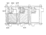
Fig. 1 represents the 1st embodiment of method for manufacturing organic EL of the present invention.This figure also is the accompanying drawing of the panchromatic method for manufacturing organic EL of expression 3 looks.This there is shown a kind of method for manufacturing organic EL, this method has: the operation that forms pixel capacitors 101,102,103 on transparency carrier 104, the pattern that forms a kind of luminescent layer 106,107 of organic compound formation on above-mentioned each pixel capacitors forms operation, form the operation of negative electrode 113, it is characterized in that the formation of above-mentioned luminescent layer is carried out according to ink-jetting style.
Transparency carrier 104 is as support and have the function of the face that takes out as light simultaneously.Therefore, transparency carrier 104 can be selected according to light transmission and thermal stability.As the transparency carrier material, for example can enumerate glass substrate, transparent plastic sheet etc., but consider, preferably glass substrate from the excellent heat resistance aspect.
At first, on transparency carrier 104, form pixel capacitors 101,102,103.As the formation method, for example can enumerate photoetching process, vacuum deposition method, sputtering method, pyrosol method etc., wherein photoetching process preferably.As pixel capacitors, preferably transparent pixel electrode as the material that constitutes transparent pixel electrode, can be enumerated: the complex oxide film of tin oxide film, ITO film, indium oxide and zinc oxide etc.
Be to form next door (baffle plate) 105 then, be used for filling up the gap between above-mentioned each transparent pixel electrode.
Adopt this method, can improve contrast, prevent the colour mixture of luminescent material, prevent light leak between pixel and the pixel etc.
Be not particularly limited as the material that constitutes next door 105, so long as the material that the solvent of EL material is had a durability gets final product, for example can enumerate: the inorganic material of the organic material of acrylic resin, epoxy resin, photosensitive polyimide etc., liquid glass etc. etc.In addition, next door 105 also can be waited and forms the black light barrier by sneak into carbon black in above-mentioned material.
As the formation method in this next door 105, for example can enumerate photoetching process etc.
And then, on each pixel capacitors, to press predetermined pattern and form organic luminous layer, organic luminous layer preferably is provided with the luminescent layer of 3 looks, and preferably at least 1 look is wherein pressed ink-jetting style formation.
According to the embodiment of Fig. 1, on pixel capacitors 101,102, press ink-jetting style respectively and form red light emitting layer 106 and green light emitting layer 107.
Herein, so-called ink-jetting style is meant, a kind of by the luminescent material dissolving or be dispersed in the solvent and the ejection liquid that forms by shower nozzle 110 ejection of inkjet-printing device 109, thus be formed on the process of the pixel of at least a kind of color in redness, green, these 3 kinds of primary colors of blueness or its Neutral colour.
According to said ink-jetting style, can be easily and form meticulous pattern at short notice.In addition, adjust thickness or by adjusting the concentration of prepared Chinese ink by the increase and decrease spray volume, promptly can be easily and freely control the illuminance of luminous harmony and brightness etc.
In addition, be under the situation of following conjugated polymer precursor when organic luminescent material, thereby can make above-mentioned precursor component conjugation (film forming) form luminescent layer by heating or rayed etc. spraying by ink-jetting style after various luminescent materials form patterns.
Then, as shown in Figure 1, on red light emitting layer 106, green light emitting layer 107 and pixel capacitors 103, form blue light-emitting layer 108.According to this method, not only can form 3 primary colors of red, green, blue, and can fill and lead up the red light emitting layer 106 and the vertical discrepancy in elevation of green light emitting layer 107, thereby make its planarization with next door 105.
Do not have particular determination as the method that forms above-mentioned blue light-emitting layer 108, for example can adopt general one-tenth such as sedimentation, warm therapy embrane method, perhaps can adopt ink-jet method to form yet.
In addition, blue light-emitting layer 108 can inject and carries the section bar material to constitute by for example resembling electronics the oxyquinoline aluminum complex.Promote the injection and the conveying of charge carrier in the case, thereby can improve luminous efficiency.And then, by with inject by following hole that the thin layer of carrying material to constitute is long-pending to stack, can make from the electronics of electrode and hole injecting evenly and be transported to luminescent layer, thereby can improve luminous efficiency further.
In addition,, can make hole injection conveying inject conveying and bear by different materials respectively, therefore can carry out optimum design to various materials respectively with electronics injecting under the folded situation of conveying section bar material equivalance with the hole.The formation method of injecting transfer layer as above-mentioned electronics does not have particular determination, for example can use general one-tenth embrane method or ink-jet methods such as sedimentation, wet method.
In addition, as forming the organic compound that electronics injects transfer layer, can enumerate: oxadiazole derivatives such as PBD, OXD-8, DSA, oxyquinoline aluminum complex, Bebq, triazole derivative, azomethine complex, porphine complexes, benzene and oxadiazole complex etc., wherein, can perhaps form electronics injection transfer layer with the mixture more than a kind or 2 kinds wherein by long-pending folding.In addition, also can in above-mentioned organic compound, be doped into following iridescent and usually form electronics injection transfer layer.In addition, above-mentioned electronics injection transfer layer also can have luminous function.
According to present embodiment, 2 looks in the organic luminous layer are pressed ink-jetting style and are formed, 1 look is pressed additive method formation in addition, therefore, even a kind of luminescent material that not too is fit to press ink-jetting style formation, also can be applicable to that other luminous organic materials of ink-jetting style make up and form panchromatic organic EL, therefore can widen scope of design with some.
As the formation method of the luminescent layer except ink-jetting style, for example can enumerate: photoetching process, vacuum deposition method, print process, transfer printing, dip coating, method of spin coating, casting method, capillary tube method, rolling method, excellent Tu Fa etc.
Form negative electrode (opposite electrode) 113 at last, thereby make organic EL of the present invention.As negative electrode 113, preferably metal film electrode as the metal that constitutes negative electrode, for example can be enumerated Mg, Ag, Al, Li etc.In addition, except these materials, some work function materials with smaller also can be used, the alloy that for example can use alkaline-earth metals such as alkali metal or Ca and contain these metals.Such negative electrode 113 can wait with sedimentation and sputtering method and form.
Organic EL of the present invention can be made by above-mentioned operation.That is to say, as shown in Figure 1, on the pixel capacitors 101 and 102 that is arranged on the transparency carrier 104, form red light emitting layer 106, the green light emitting layer 107 that constitutes by organic compound with ink-jetting style by pattern separately, and then on above-mentioned luminescent layer 106,107 and pixel capacitors 103, form blue light-emitting layer 108 with vacuum deposition method.Form negative electrode 113 at last in the above, thereby finished organic EL of the present invention.
Then, as shown in Figure 6, on negative electrode 413, form diaphragm 415.Owing to formed diaphragm 415, therefore can prevent negative electrode 413 and each luminescent layer 406,407,408 deterioration, damage and peel off etc.
As the constituent material of said protection film 415, can enumerate epoxy resin, acrylic resin, liquid glass etc.In addition, as the formation method of diaphragm 415, for example can enumerate: method of spin coating, casting method, dip coating, rod are coated with method, rolling method, capillary tube method etc.
Luminescent layer preferably is made of organic compound, more preferably is made of macromolecular organic compound.By forming the luminescent layer that constitutes by organic compound, can be issued to the surface light emitting of high brightness in the condition of low-voltage.In addition, because luminescent material can be selected in wide region, therefore can reasonably design the EL light-emitting component.
Particularly the film forming of macromolecular organic compound is good, and the luminescent layer that is made of macromolecular organic compound has utmost point favorable durability.In addition, these macromolecular organic compounds have the band gap of visible region and higher conductivity, and wherein, the high molecular this tendency of conjugated system is remarkable especially.
As the organic light emission layer material, can use macromolecular organic compound itself, perhaps use can be by heating the precursor etc. of the conjugated polymer organic compound of conjugation (film forming).
Using under the situation of conjugation (film forming) precursor before as luminescent material, as the ejection liquid of ink-jet, its viscosity etc. are adjusted easily, can carry out accurate pattern-forming, and can easily control the characteristics of luminescence of luminescent layer and the proterties of filming.
Be used to form the macromolecular organic compound of luminescent layer, preferably the hole is injected and is carried the section bar material.Can promote the injection and the conveying of charge carrier like this, thereby improve luminous efficiency.
As the organic compound that can form luminescent layer, for example can enumerate: PPV (poly-(to inferior phenylethylene)) or derivatives thereof, PTV (poly-(2, the inferior ethene of the inferior thiophene of 5-)) the inferior thiophene of poly-alkyl, PFV (poly-(2 such as, the inferior ethene of the inferior furans of 5-)), poly (arylene ether) ethene, pyrazoline dimer, quinolizine (quinolidine) carboxylic acid, perchloric acid benzopyralium salt, benzene such as poly, poly alkyl fluorene open pyrans quinolizine, rubrene, phenanthroline europium complex etc., can use the mixture more than a kind or 2 kinds wherein.
The PPV or derivatives thereof that wherein preferably belongs to the conjugated polymer organic compound.In PPV or derivatives thereof conjugation (film forming) the precursor water soluble or organic solvent before, therefore be suitable for carrying out pattern and form with ink-jetting style.In addition, owing to be macromolecule, therefore can obtain high-quality and film that its durability is good on a kind of optics.In addition, the PPV or derivatives thereof has strong fluorescence, and it is a kind of macromolecule of conductivity, so the non-localized electronics of the electricity of the π on its two keys on polymer chain, therefore the PPV film has the function that transfer layer is injected in the hole, can obtain a kind of high performance organic EL.
In addition, under the situation of using macromolecule organic light emission layer material, the organic EL composition also can contain at least a kind of fluorchrome.Can change the characteristics of luminescence of luminescent layer like this, for example can improve the luminous efficiency of luminescent layer effectively, perhaps as the effective means that changes the very big wavelength of light absorption (illuminant colour).
That is to say that fluorchrome does not just use as the luminescent layer material, and use as the dye material of bearing lighting function.For example,, can almost entirely transfer on the fluorchrome molecule again in conjunction with the energy of the exciton that generates by the charge carrier on such conjugated system macromolecular organic compound molecule such as PPV.In the case, the light that sends only is to be produced by the high fluorchrome molecule of a kind of fluorescence quantum efficiency, so the electric current quantum efficiency of EL element has also improved.And, by in the organic EL composition, adding fluorchrome, can therefore can be effective as the means that are used to change glow color so that the spectrum that luminescent layer sends becomes the spectrum of fluorescence molecule simultaneously.
In addition, so-called herein electric current quantum efficiency is one and is used to investigate the yardstick of luminescent properties according to lighting function that it can define by following formula.
η
εThe electric energy of the energy/input of=photon of emitting
So, change the very big wavelength of light absorption by the doping fluorescent pigment, can make its light that sends 3 kinds of for example red, blue, green primary colors, consequently can obtain a kind of panchromatic display unit.
In addition, by the doping fluorescent pigment, can improve the luminous efficiency of EL element significantly.
As the fluorchrome that is applicable in the red light emitting layer, can use the DCM that belongs to the laser pigment or the derivative of rhodamine or rhodamine, Yi is Ji compounds such as perylenes.Therefore these fluorchromes are low-molecular-weight, dissolve in the solvent, and the intermiscibility of they and PPV etc. are good, and form a kind of even and stable luminescent layer easily.As rhodamine derivatives fluorescent pigment, for example can enumerate: rhodamine B, rhodamine B alkali, rhodamine 6G, rhodamine 101 perchlorate etc., these pigments also can be the mixtures more than 2 kinds.
In addition, as the fluorchrome that is applicable in the green light emitting layer, can enumerate: quinoline a word used for translation ketone, rubrene, DCJT and their derivative.Therefore these fluorchromes and above-mentioned red fluorescence pigment similarly are low-molecular-weight, dissolve in the solvent, and in addition, they are good with the intermiscibility of PPV, therefore formation luminescent layer easily.
As the fluorchrome that is applicable to blue light-emitting layer, can enumerate distyryl biphenyl and derivative thereof.These fluorchromes are also the same with above-mentioned red fluorescence pigment to be soluble in the aqueous solution, and good with the intermiscibility of PPV, therefore forms luminescent layer easily.
In addition, other can be enumerated: the coumarin derivative of cumarin and coumarin-1, cumarin-6, coumarin-7, cumarin 120, cumarin 138, cumarin 152, cumarin 153, cumarin 311, cumarin 314, cumarin 334, cumarin 337, cumarin 343 etc. as the fluorchrome that is applicable in the blue light-emitting layer.
In addition, other can be enumerated: tetraphenylbutadiene (TPB) or TPB derivative, DPVBi etc. as the luminescent material that is applicable in the blue light-emitting layer.These luminescent materials are also the same with above-mentioned red fluorescence pigment etc. to be low-molecular-weight, therefore dissolve in the solvent, and they is good with the intermiscibility of PPV etc., therefore formation luminescent layer easily.
Above fluorchrome and luminescent material can use the mixture more than a kind or 2 kinds wherein.
The ink-jet of using in method for manufacturing organic EL of the present invention is shown among Figure 10 and Figure 11 with the structure of shower nozzle.
When this ink-jet had the nozzle plate 11 of stainless steel for example and oscillating plate 13 with shower nozzle 10, the two was joined together by isolated component (storage plate) 15.
Between nozzle plate 11 and oscillating plate 13, form a plurality of spaces 19 and reservoir 21 by isolated component 15.The inside of each space 19 and reservoir 21 is full of composition of the present invention, and each space 19 is interconnected by supply port 23 with hopper 21.
In addition, being provided with one on nozzle plate 11 is used for from the composition in space 19 nozzle bore 25 with the jet-like ejection.On the other hand, on oscillating plate 13, form a hole 27 that is used for composition is infeeded reservoir 21.
In addition, with oscillating plate 13 on the surface of a surperficial relative side in space 19, be bonded with piezoelectric element 29 accordingly with the position in above-mentioned space 19.
This piezoelectric element 29 is between the pair of electrodes 31, in case feed electric current, the just outstanding laterally deflection of piezoelectric element 29, simultaneously, the oscillating plate 13 that is bonded together with piezoelectric element 29 also becomes integral body deflection laterally.So just increased the volume in space 19.Therefore, suitable with the space 19 interior that part of volumes that increase composition just passes through supply port 23 by in reservoir 21 inflow spaces 19.
Then, in case remove the electric current that feeds piezoelectric element 29, this piezoelectric element 29 and oscillating plate 13 just recover its original state immediately.Therefore this time space 19 also returns to original volume, makes the pressure of composition of 19 inside, space rise, thereby causes composition to be sprayed to substrate by nozzle bore 25.
In addition, be provided with hydrophobic layer 26, so that prevent the crooked and spray orifice obstruction of the flight approach of composition at the peripheral position of nozzle bore 25.
That is to say,, for example be provided with the hydrophobic layer 26 that the electrodeposited coating by the eutectoid of Ni-tetrafluoroethene constitutes as shown in Figure 11 at the peripheral position of nozzle bore 25.
Act on such shower nozzle,, so just formed pixel by forming each organic luminous layer by the predetermined pattern ejection composition corresponding with red, blue, green 3 urine form and aspect.
In method for manufacturing organic EL of the present invention, the luminous organic material composition as being applicable to ink-jetting style can use the composition with following characteristic.
The nozzle that is used to spray above-mentioned composition is arranged on ink-jet with shower nozzle, and therefore, said composition is preferably 30 °~170 °, more preferably 35 °~65 ° with respect to the contact angle of the material of the nozzle face 251 that constitutes said nozzle.Because therefore the contact angle that said composition has above-mentioned scope can suppress the bending of said composition flight approach, thereby can form accurate pattern.
That is to say that when 30 ℃ of this contact angle less thaies, composition increases with respect to the wetability of nozzle face constituent material, therefore when the ejection said composition, said composition is sometimes asymmetricly attached to around the nozzle bore.In the case, there is graviational interaction in composition attached to nozzle bore each other with the composition that is ejected, because said composition is subjected to uneven active force when ejection, therefore the what is called flight bending of target location has taken place to reach, and the crooked frequency of flight increases also.In addition, if above 170 °, then the interaction between composition and the nozzle bore is minimum, and therefore the meniscus shape instability at nozzle tip place becomes difficult to composition spray volume and ejection control regularly.
So-called herein flight bending is meant that when composition was sprayed by said nozzle, the hit location of composition drop was for the skew more than 50 μ m take place in the target location.In addition, the crooked frequency of so-called flight is meant that the composition drop begins the time of frequency ejection when the above-mentioned flight of generation is crooked with 7200Hz.If the flight curved major is because the wetability of nozzle bore is inhomogeneous or owing to cause that nozzle bore obstruction etc. takes place adhering to of composition solid composition, this phenomenon can be eliminated by the method for cleaning shower nozzle.The crooked frequency of this flight is high more, just must carry out frequent more cleaning to shower nozzle, and therefore so a kind of meeting composition that the crooked frequency of flight is increased can be described as a kind of composition that causes by the manufacturing efficient reduction of the EL element of ink-jetting style.With regard to realistic scale, the crooked frequency of flight must be more than 1000 seconds.
Owing to can prevent such flight bending, therefore can form high meticulous pattern, and can carry out accurately.
In addition, the viscosity of above-mentioned composition is preferably 1cp~20cp, more preferably 2cp~4cp.When the viscosity deficiency 1cp of composition, above-mentioned precursor and the fluorchrome content in said material is too small, thereby makes the luminescent layer that forms can not bring into play luminous power fully.On the other hand, when surpassing 20cp, composition can not if do not take the measure of change device specifications such as enlarged nozzle aperture, then be difficult to carry out pattern-forming successfully from the nozzle bore ejection.In addition, when viscosity was excessive, the solid constituent in the composition was separated out easily, thereby made the blocked generation frequency of nozzle bore increase.
In addition, the surface tension of above-mentioned composition is preferably 20dyne/cm~70dyne/cm, more preferably 25dyne/cm~40dyne/cm.By surface tension is in the above-mentioned scope, just can suppress the flight bending, and the crooked frequency that will fly is suppressed to than low degree with the situation of above-mentioned contact angle the samely.If the not enough 20dyne/cm of surface tension, then composition increases the wetability of nozzle constituent material, thereby can produce the flight bending with the situation of above-mentioned contact angle the samely, and the crooked frequency of flight is increased.In addition, if surface tension above 70dyne/cm, then in the meniscus shape instability at nozzle tip place, therefore becomes difficult to composition spray volume and ejection control regularly.
In addition, luminous organic material composition as the manufacture method that is applicable to the organic E L of the present invention element, as long as can satisfy at least one number range in above-mentioned contact angle, viscosity and the surface tension, preferably can satisfy the composition of the characteristic condition of 2 above combination in any in the above-mentioned parameter, be more preferably the composition that can satisfy all characteristics.
Fig. 2 illustrates the embodiment 2 of method for manufacturing organic EL of the present invention.
In the present embodiment, on transparent base 204, form pixel capacitors 201,202,203 and next door 205 similarly to Example 1, press ink-jetting style then and form red light emitting layer 206, green light emitting layer 207.
Be with the foregoing description 1 difference, on pixel capacitors 203, form the hole and inject transfer layer 208, and then area folded blue light-emitting layer 210 on this layer.Inject transfer layer 208 by so long-pending folded hole, promoted to come as mentioned above the injection and the conveying in the hole of self-electrode, thereby can improve luminous efficiency.
Like this, in method for manufacturing organic EL of the present invention, preferably carry lamination to gather into folds the luminescent layer and the hole injection of at least 1 look.So just luminous efficiency can be improved, and the stability of thin-film component itself can be further improved.
In addition, inject the near interface of transfer layer in long-pending folded luminescent layer and hole, two-layer in separately the part of contained material also can exist mutually to his layer one side infiltration and the state that spreads.
The preferably non-luminous layer of transfer layer 208 is injected in the hole.So just can make blue light-emitting layer 210 on pixel capacitors 203, become illuminating part, thereby can make panchromatic organic EL with comparalive ease.
The formation method that transfer layer 208 is injected in above-mentioned hole is not particularly limited, and for example can form by ink-jetting style.So just can dispose this hole and inject transfer layer 208 according to the good predetermined pattern of precision.
Constituent material as hole transporting layer 208, for example can enumerate: phthalocyanines complex, porphines compounds, NPD, TAD, polyanilines etc. such as the aromatic diamine compounds of TPD etc., MTDATA, quinoline a word used for translation ketone, bisstil anthracene derivant, PVK (polyvinylcarbazole), CuPc wherein are preferably PVK.By using PVK, can form non-luminous hole and inject transfer layer.
And then, similarly form blue light-emitting layer 210 and negative electrode 211 with the foregoing description 1, so promptly can obtain organic EL of the present invention.The constituent material of blue light-emitting layer 210, negative electrode 211 and formation method are same as the previously described embodiments.
Fig. 3 illustrates the embodiment 3 of the organic E L of the present invention manufacturing method.
In the present embodiment, pixel capacitors 301,302,303 and next door 305 are set on transparent base 304 similarly to Example 1, by ink-jetting style red light emitting layer 306 and green light emitting layer 307 are set then.
On the entire area above red light emitting layer 306, green light emitting layer 307 and the pixel capacitors 303, form the hole then and inject transfer layer 308.As mentioned above, by the hole being injected transfer layer 308 and luminescent layer 306 and 307 long-pending gathering into folds, can promote the injection and the conveying in hole, thereby can improve luminous efficiency.
In addition,, inject transfer layer 308, non-luminous layer preferably is set as the hole according to reason same as described above.
The formation method of above-mentioned hole being injected transfer layer 308 is not particularly limited, and for example can enumerate: ink-jetting style, vacuum deposition method, dip coating, method of spin coating, casting method, capillary tube method, rolling method, excellent Tu Fa etc.Can form by vacuum deposition method in the present embodiment.In addition, the constituent material as hole injection transfer layer can use and the foregoing description 2 identical materials.
Inject formation blue light-emitting layer 309 and negative electrode 311 on the transfer layer 308 then in the hole, can obtain organic EL of the present invention like this.The constituent material of negative electrode 311 and formation method are same as the previously described embodiments.
Fig. 4 illustrates the embodiment 4 of organic EL manufacture method of the present invention.
In the present embodiment, on transparent base 804, form pixel capacitors 801,802,803 and next door 805 similarly to Example 1, on pixel capacitors 801,802,803, press pattern with ink-jetting style separately then and form luminescent layer 806,806 and 808.So just can be easily and easily to spray volume, the ejection number of times of for example each luminescent layer material with form pattern and regulate, and can be easily the proterties of films such as the characteristics of luminescence of each luminescent layer, thickness be controlled.
On each luminescent layer 806,807,808, form electronics then and inject transfer layer 811.Electronics injects transfer layer 811 can make the electronics from negative electrode easily inject, and in addition, because luminous component away from negative electrode, therefore can prevent the electrode delustring, and can contact preferably with negative electrode formation.Inject transfer layer 811 as electronics, can use the oxyquinoline aluminum complex of undoped.Above-mentioned electronics injects transfer layer 811 and can form by vacuum deposition method.
In addition, the formation method of electronics being injected transfer layer 811 is unqualified, and for example it can be ink-jet method, vacuum deposition method, dip coating, method of spin coating, casting method, capillary tube method, rolling method, excellent Tu Fa etc.
And then form negative electrode 813 in the above, thereby obtained organic EL of the present invention.The constituent material of negative electrode 813 and formation method are same as the previously described embodiments.
Fig. 5 illustrates the embodiment 5 of the organic E L of the present invention manufacturing method.
In the present embodiment, pixel capacitors 801,802 and 803 is set at first similarly to Example 1 on transparent base 804.Form one deck with whirl coating on the entire area above it again and for example inject transfer layer 815 by the hole that PVK constitutes.Need just can all not apply the hole like this and inject transfer layer 815 and make its film forming, therefore can improve manufacturing efficient through pattern-forming.
In addition, the formation method of the hole being injected transfer layer 815 is unqualified, and for example it can be ink-jet method, vacuum deposition method, dip coating, method of spin coating, casting method, capillary tube method, rolling method, excellent Tu Fa etc.
In addition, according to above-mentioned same reason, the preferably non-luminous layer of transfer layer 815 is injected in the hole.
Inject in the hole then and form luminescent layer 806,807 and 808 on the transfer layer 815.Wherein have at least the luminescent layer of 1 look preferably to use ink-jet printing apparatus 809, form pattern according to ink-jet method.
And then on luminescent layer, form negative electrode 813, thereby obtained organic E L element of the present invention.The constituent material of negative electrode 813 and formation method are same as the previously described embodiments.
In addition, the next door is not set in the manufacture method of present embodiment, but, just can carries out the coating of R, G, B accurately respectively, thereby can improve manufacturing efficient as long as according to method for manufacturing organic EL of the present invention.But also can the next door similarly be set to form each pixel respectively with the foregoing description.
Though organic EL of the present invention can be made by aforesaid method, is not limited to these methods, for example it also can have following formation.
Figure 15 is the partial cross section figure of expression another example of organic EL of the present invention.
The organic EL of present embodiment is that the folded reflector 62 of area, transparent and electrically conductive film (ITO film) 63, hole are injected transfer layer 64, organic luminous layer 65, metal level 66, transparent and electrically conductive film (ITO film) 67 and constituted in turn on transparency carrier 61.Material and formation method to each layer describes below, but the item identical with the various embodiments described above then omitted its explanation, and their difference only is described.
The organic EL of present embodiment directly is provided with the reflector 62 that one deck is made of the metallic film of Al etc. on transparency carrier 61.
In addition, as negative electrode and the long-pending metal level 660 minutes thin (about 10~50A) that is stacked on the luminescent layer 65, so it has light transmission, can see through the coloured light that is sent by luminescent layer 65.On the other hand, because it is very thin, so its resistance value height, conductivity is good inadequately, can not give full play to the function as negative electrode, so amass the conductive film (ITO film) 67 of folded layer of transparent on metal level 66.In addition, if such metal level 66 is made of for example Al-Li alloy etc., can adopts sedimentation or sputtering method to wait in the case and form.
Owing to have such formation, the electric current that is injected by electrode just sees through according to the direction shown in the figure arrow at the light that luminescent layer 65 converts to.Therefore, need just light can not taken out, thereby can obtain the more demonstration of high brightness by transparency carrier 61.
Fig. 7 represents an example of organic E L display unit of the present invention.
In the present embodiment, on glass plate 501, form a kind of bus (gate line) 511 of Al system by the lithographic imagery method, the thin-film transistor that does not illustrate among the formation figure in the above then, and then form 504 etc. ITO transparent pixel electrode.Press ink-jetting style then similarly to Example 1 and form luminescent layer 502 (red), 503 (green), and then press vacuum deposition method formation blue light-emitting layer 505.Form negative electrode 506 with vacuum deposition method then, so just made the organic EL same with the foregoing description 1.
To protect base material 507 to be fitted in regularly on the transparency carrier 501 afterwards by perimeter seal 509.
Then, this display unit is placed in the inert gas atmosphere such as argon gas, imports inert gases 512 by sealing of hole 513, at last with sealing material 508 with sealing of hole 513 sealings.Owing to be encapsulated into inert gas 512, can prevent that therefore organic EL is subjected to moisture etc. from the pollutant of outside and the influence of environmental change, thereby can keep the luminescent properties of organic EL display.Sealing material 508 preferably is made of the material that can not see through inert gas 512.
Fig. 8 illustrates an example of the active matrix organic EL display device that uses organic EL of the present invention.The organic EL display of this embodiment is by matrix-shaped configurations, and has the visual configurations shown that many light-emitting pixels that the illuminating part by R, G, B forms constitute separately.
As shown in the drawing, on the substrate (not shown), form many holding wire (signal electrode) 601 and gate lines (grid) 602 by mutually orthogonal arrangement, in each pixel, all has the thin-film transistor (TFT) 604 that is connected with gate line 602 with holding wire 601, this TFT604 and the luminescent layer that forms by organic EL 605,606 long-pending the stacking that are connected in the above.In addition, in organic luminous layer, have at least the luminescent layer of 1 look to form by ink-jetting style.
Fig. 9 is the sectional view of expression active matrix organic EL display device of the present invention.
At first on transparency carrier 904, form the gate line that do not illustrate among predetermined thin-film transistor 915 and the figure, holding wire etc.On each pixel capacitors (ITO) 901,902,903, form the hole that is covered with each pixel capacitors then and inject transfer layer 911 with these thin-film transistor 915 elements such as predetermined function such as grade.Inject conveying section bar material as the hole, can use the material same with the foregoing description.In addition, the formation method that transfer layer 911 is injected in the hole is not particularly limited, and it can form by above-mentioned any method.
And then form each luminescent layer 906 (red), 907 (green), 908 (baskets) by pattern.The formation of luminescent layer can use inkjet-printing device 910 to form the wherein luminescent layer of at least 1 look according to ink-jetting style.
In the foregoing description of active matrix organic EL display device of the present invention, though be to use thin-film transistor as switch element, unqualified to this, also can use switch element, the diode of other kinds, for example switch element such as MIM.Also can adopt passive drive, static drive (still image, local display) etc. in addition.
In addition, pixel only is not limited to can be equipped with a plurality of switch elements with a switch element for a pixel.
Figure 12 illustrates the example that is equipped with the organic EL display of a plurality of switch elements for a pixel.In the case, switching thin-film transistor 142 is according to the current potential of scan electrode 131, the current potential of signal electrode 132 is conveyed to current film transistor 143, and this current film transistor 143 plays a kind of control action for the conducting of public electrode 133 and pixel capacitors 141.
Explain an example of passive matrix (simple matrix) the type organic EL display that uses organic EL of the present invention below with reference to the accompanying drawings.
Figure 13 is the summary part amplification sectional view of organic EL display of the present invention.
As shown in the figure, in the organic EL display of present embodiment, when making organic EL, thin rectangular scan electrode 53 and signal electrode 54 mutually orthogonal configuration by organic EL 52.
The driving of such passive matrix can be undertaken by following mode, just selects scan electrode 53 in turn with pulse mode, when selecting this scan electrode 53, selects simultaneously to apply voltage with the corresponding signal electrode 54 of each pixel and to it.Such selection can be controlled by controller 55.
Should illustrate that under the situation of passive drive type, negative electrode (cathode) must form pattern, so that each bar line is separated.For example, in the 3rd embodiment of the present invention, when to form thickness be thin negative electrode about 0.2 μ m, this negative electrode was separated by the next door, so just becomes the state that forms pattern naturally.
Negative electrode can carry out pattern according to for example mask deposition method, laser cutting method and form.
An example that applies the driven waveform of voltage to scan electrode 13 and signal electrode 14 has been shown among Figure 14.In the drive waveforms shown in this figure, applying to the pixel of selecting is enough to make its luminous voltage V
SIn addition, according to the pulse amplitude waveform that is consistent with gradation, can control the display density of pixel.On the other hand, then be applied to voltage Vn below the lasing threshold voltage for non-selected pixel.
In Figure 14, Tf represents the operating time.In the case, be 1/100 to drive by duty ratio.In addition, the light that the blue light-emitting layer 808 of the organic EL display that is made of the organic EL of the foregoing description 4 is sent, when driving voltage was 20V, its brightness was 100cd/m
2
(embodiment)
[manufacturing of organic EL]
(embodiment 1)
As shown in Figure 1, on glass substrate 104, form ITO transparent pixel electrode 101,102 and 103, thereby form 100 μ m spacings and the thick pattern of 0.1 μ m by photoetching process.
Bury the space between the ITO transparent pixel electrode then, form a kind of next door 105 that has shading concurrently and prevent two kinds of effects of ink loss with photoetching process again.The wide of this next door 105 is 20 μ m, and thick is 2.0 μ m.
And then, utilize the shower nozzle 110 ejection tables 1 of ink-jet printing apparatus 109 and the redness shown in the table 2, green various luminescent materials to form pattern, then in nitrogen atmosphere under 150 ℃ temperature heat treated 4 hours, make the precursor polymeric in the composition become macromolecule whereby, thereby form each luminescent layer 106 (red) and 107 (green).
Utilize condensation aromatic compound that a kind of interpolation has a perylene to carry out vacuum deposition as the hydroxyquinoline aluminum of dopant then, the electronics that forms one deck 0.1 μ m whereby injects the blue light-emitting layer 108 of carrying stratotype.
At last with sedimentation form a layer thickness be the Mg-Ag electrode 113 of 0.8 μ m as negative electrode, thereby made organic EL.
(embodiment 2)
Similarly to Example 1, by the ITO transparent pixel electrode 201,202 and 203 that on glass substrate 204, forms shown in Figure 2, bury the space between the ITO transparent pixel electrode then, and then form the barrier wall (next door) 205 that has shading concurrently and prevent the photosensitive polyimide of two kinds of effects of ink loss.
And then use an ink-jet printing apparatus 209 similarly to Example 1, press the various luminescent materials of the redness shown in pattern coating table 1 and the table 2, green, heat treated 4 hours in nitrogen atmosphere and under 150 ℃ the temperature then, make the precursor polymeric in the composition become macromolecule whereby, thereby form each luminescent layer 206 (red) and 207 (green).
Use above-mentioned ink-jet printing apparatus 209 then, on transparent pixel electrode 203, press pattern and form the hole injection transfer layer that one deck is made of polyvinylcarbazole (PVK).Then apply one deck pyrazoline dimer in the above, thereby formed blue light-emitting layer 210.
At last with sedimentation form a layer thickness be the Al-Li electrode 211 of 0.8 μ m as negative electrode, thereby made organic EL.
(embodiment 3)
At first similarly to Example 1, by ITO transparent pixel electrode 801,802,803 and the next door 805 of on glass substrate 804, forming shown in Figure 4.
In the luminescent material shown in table 1 and the table 2, sneak into organic hole then and inject conveying section bar material, use an inkjet-printing device 809 to form each luminescent layer 806 (red), 807 (green) and 808 (indigo plants).
Use a kind of oxyquinoline aluminum complex of undoped to carry out vacuum deposition then, having formed a layer thickness is the electronics injection transfer layer 811 of 0.1 μ m.
Form the AL-Li electrode 813 that a layer thickness is 0.2 μ m with sedimentation at last, thereby made organic EL.
(embodiment 4)
Similarly to Example 1, by each ITO transparent pixel electrode 301,302,303 and next door 305 of on glass substrate 304, forming shown in Figure 3.
Use an ink-jet printing apparatus 310 then similarly to Example 1, press the various luminescent materials of the redness shown in pattern coating table 1 and the table 2, green, heat treated 4 hours in nitrogen atmosphere and under 150 ℃ the temperature then, make the precursor polymeric in the composition become macromolecule whereby, thereby form each luminescent layer 306 (red) and 307 (green).
On the entire area on luminescent layer 306,307 and the transparent pixel electrode 303, form one deck then and inject transfer layer 308 by the hole that polyvinylcarbazole (PVK) constitutes with coating process.
Then inject on the transfer layer 308 and form the blue light-emitting layer 309 that one deck is made of the distyrene derivative with vacuum deposition method in the hole.
At last with sedimentation form a layer thickness be the Al-Li electrode 311 of 0.8 μ m as negative electrode, thereby made organic E L element.At this moment, as mentioned above, negative electrode 311 is separated by next door 305 and naturally by its insulation, and each pixel capacitors 301,302,303 is common to constitute pattern states thereby make.
(embodiment 5)
At first similarly to Example 1, by ITO transparent pixel electrode 801,802,803 and the next door 805 of on glass substrate 804, forming shown in Figure 4.
And then use the macromolecule luminous organic material shown in ink-jet printing apparatus 809 ejection tables 1 and the table 2, apply luminescent material of all kinds by pattern, heat treated 4 hours in nitrogen atmosphere and under 150 ℃ the temperature then, make the precursor polymeric in the composition become macromolecule whereby, can send redness, green and blue each luminescent layer 806 (red), 807 (green) and 808 (indigo plants) thereby form.
Use a kind of oxyquinoline aluminum complex of undoped to carry out vacuum deposition then, having formed a layer thickness is the electronics injection transfer layer 811 of 0.1 μ m.
At last with sedimentation form a layer thickness be the Al-Li electrode 812 of 0.8 μ m as negative electrode, thereby made organic EL.
2. to the evaluation of the luminescent properties and the film properties of luminescent layer
Luminescent properties and film properties for the luminescent layer of the organic EL that makes in the foregoing description 1~5 are estimated as follows.
1. luminous beginning voltage
Apply predetermined voltage to element, observing 1cd/m
2Luminosity the time the voltage that applies be defined as luminous beginning voltage [Vth].
2. luminescent lifetime
, apply certain electric current by reference waveform and make it luminous continuously as 100% with the initial stage brightness after the stabilization processes, measure the variation of its brightness, 50% o'clock the timing definition that begins to be lower than initial stage brightness with its brightness is a luminescent lifetime.
Should illustrate that drive condition is: room temperature: 40 ℃; Humidity: 23%; Current value: 20mA/cm
2
3. luminosity
At current value is 20mA/cm
2The time brightness that records.
4. absorb very big wavelength
Measure the very big wavelength of absorption of each luminescent layer.
5. become membrane stability
With luminescent layer at 200 ℃ down after the heating 60 minutes, situation about taking place with defectives such as the crackle of microscopic examination luminescent layer or distortion.
Estimate and carry out in the following manner.
◎ ... very good
Zero ... well
* ... bad
Institute obtains and the results are shown in table 3 and the table 4.
Shown in table 3 and table 4, in any embodiment of embodiment 1~5, the luminescent properties of each luminescent layer and the film properties of luminescent layer are all good.Particularly under the situation that luminescent layer is made of macromolecular organic compound, do not observe defective fully in each luminescent layer, this explanation has formed very good film.
Abovely explained organic EL of the present invention with composition and method for manufacturing organic EL, but the present invention is not subjected to the qualification of these embodiment, for example, can be arranged in the operation that forms any functional intermediate layer between each layer yet according to illustrated each embodiment.In addition, also without limits for the fluorchrome that adds in order to change luminescent properties.
In addition, also can form one deck for example by 1,2 between each layer, the layer that 4-triazole derivative (TAZ) constitutes can improve luminosity and luminescent lifetime etc. so further as resilient coating.
In addition, in method for manufacturing organic EL of the present invention, be easy to adhere to, can have and the surface of resin protection film, pixel capacitors and bottom be carried out surface-treated operations such as plasma treatment, UV processing, coupling in order to make the EL material.In addition, method for manufacturing organic EL of the present invention also can be applied in the manufacture method of inorganic EL element.
In addition, organic E L display unit of the present invention can be applied to local display or simultaneously luminous comprehensively still image shows, for example the field of low amount of information such as picture, literal, famous brand perhaps, also can be used as the light source with point, line, surface shape and uses.
As mentioned above, according to method for manufacturing organic EL of the present invention,, can reasonably design the EL light-emitting component by in relative broad range, selecting luminescent material.For example, by luminescent material and fluorchrome are made up etc., can obtain various display lights.
In addition, by using luminous organic material, can launch the design of relevant high brightness and long-life various EL element.
In addition, by injecting transfer layer and electronics injects transfer layer in organic luminous layer, the hole of pressing that the ink-jetting style according pattern forms and arranging at least 1 look, can be arbitrarily and critically set the size or the pattern of light-emitting component.
Using under a kind of situation of precursor as luminescent material that can make its conjugation (film forming), the degree of freedom of condition enactments such as viscosity is increased, can easily adjust the condition of ink-jet that be suitable as with ejection liquid by being heating and curing.
In addition, according to method for manufacturing organic EL of the present invention, therefore condition such as can at random adjust thickness, count can easily control the luminescent properties of luminescent layer.
In addition,, shower nozzle is freely moved on transparency carrier, therefore, to the size of substrate without limits, can form the element of any size according to ink-jetting style.In addition, owing to can the position of the material configuration of necessary amount in appointment will be only limited to, therefore can farthest avoid the refuse of degree of generation liquid etc.Thereby can make the full color display of big picture at an easy rate.


Claims (2)
1. a method of making organic electroluminescent device comprises the following steps:
Form a plurality of pixel electrodes on substrate, described a plurality of pixel electrodes comprise first pixel electrode, second pixel electrode and the 3rd pixel electrode;
By ink-jet method, on described first pixel electrode, form red light emitting layer;
By ink-jet method, on described second pixel electrode, form green light emitting layer;
On described the 3rd pixel electrode, described red light emitting layer and described green light emitting layer, form blue light-emitting layer;
On described blue light-emitting layer, form opposite electrode.
2. the method for manufacturing organic electroluminescent device as claimed in claim 1 is characterized in that, carries out the step that forms described blue light-emitting layer by vacuum deposition method.
Applications Claiming Priority (2)
| Application Number | Priority Date | Filing Date | Title |
|---|---|---|---|
| JP31382896A JP3899566B2 (en) | 1996-11-25 | 1996-11-25 | Manufacturing method of organic EL display device |
| JP313828/1996 | 1996-11-25 |
Related Parent Applications (1)
| Application Number | Title | Priority Date | Filing Date |
|---|---|---|---|
| CNB2003101102998A Division CN100392891C (en) | 1996-11-25 | 1997-11-25 | Method of manufacturing organic el element, organic el element, and organic el display device |
Publications (2)
| Publication Number | Publication Date |
|---|---|
| CN1897295A CN1897295A (en) | 2007-01-17 |
| CN100477251C true CN100477251C (en) | 2009-04-08 |
Family
ID=18046006
Family Applications (5)
| Application Number | Title | Priority Date | Filing Date |
|---|---|---|---|
| CNA2006101016534A Pending CN1905157A (en) | 1996-11-25 | 1997-11-25 | Organic EL element and method of manufacturing organic EL element, and organic EL display device |
| CN2006101016623A Expired - Lifetime CN1953239B (en) | 1996-11-25 | 1997-11-25 | Method of manufacturing organic el element, organic el element, and organic el display device |
| CNB971925461A Expired - Lifetime CN1138458C (en) | 1996-11-25 | 1997-11-25 | Organic EL elements and its producing method and organic EL display device |
| CNB2003101102998A Expired - Lifetime CN100392891C (en) | 1996-11-25 | 1997-11-25 | Method of manufacturing organic el element, organic el element, and organic el display device |
| CNB200610101652XA Expired - Lifetime CN100477251C (en) | 1996-11-25 | 1997-11-25 | Method for manufacturing organic el element |
Family Applications Before (4)
| Application Number | Title | Priority Date | Filing Date |
|---|---|---|---|
| CNA2006101016534A Pending CN1905157A (en) | 1996-11-25 | 1997-11-25 | Organic EL element and method of manufacturing organic EL element, and organic EL display device |
| CN2006101016623A Expired - Lifetime CN1953239B (en) | 1996-11-25 | 1997-11-25 | Method of manufacturing organic el element, organic el element, and organic el display device |
| CNB971925461A Expired - Lifetime CN1138458C (en) | 1996-11-25 | 1997-11-25 | Organic EL elements and its producing method and organic EL display device |
| CNB2003101102998A Expired - Lifetime CN100392891C (en) | 1996-11-25 | 1997-11-25 | Method of manufacturing organic el element, organic el element, and organic el display device |
Country Status (8)
| Country | Link |
|---|---|
| US (7) | US6863961B2 (en) |
| EP (4) | EP1376716B1 (en) |
| JP (1) | JP3899566B2 (en) |
| KR (4) | KR100495744B1 (en) |
| CN (5) | CN1905157A (en) |
| DE (2) | DE69727212T2 (en) |
| TW (1) | TW553579U (en) |
| WO (1) | WO1998024271A1 (en) |
Families Citing this family (481)
| Publication number | Priority date | Publication date | Assignee | Title |
|---|---|---|---|---|
| US5989945A (en) * | 1996-05-15 | 1999-11-23 | Seiko Epson Corporation | Thin film device provided with coating film, liquid crystal panel and electronic device, and method for making the thin film device |
| JP3899566B2 (en) * | 1996-11-25 | 2007-03-28 | セイコーエプソン株式会社 | Manufacturing method of organic EL display device |
| US6462722B1 (en) | 1997-02-17 | 2002-10-08 | Seiko Epson Corporation | Current-driven light-emitting display apparatus and method of producing the same |
| WO1998036407A1 (en) | 1997-02-17 | 1998-08-20 | Seiko Epson Corporation | Display device |
| JP3520396B2 (en) | 1997-07-02 | 2004-04-19 | セイコーエプソン株式会社 | Active matrix substrate and display device |
| JP3541625B2 (en) * | 1997-07-02 | 2004-07-14 | セイコーエプソン株式会社 | Display device and active matrix substrate |
| US6843937B1 (en) * | 1997-07-16 | 2005-01-18 | Seiko Epson Corporation | Composition for an organic EL element and method of manufacturing the organic EL element |
| GB9715907D0 (en) | 1997-07-29 | 1997-10-01 | Cambridge Consultants | Electroluminescent device production process |
| US6380672B1 (en) | 1997-08-21 | 2002-04-30 | Seiko Epson Corporation | Active matrix display device |
| JP3830238B2 (en) | 1997-08-29 | 2006-10-04 | セイコーエプソン株式会社 | Active matrix type device |
| GB9718516D0 (en) | 1997-09-01 | 1997-11-05 | Cambridge Display Tech Ltd | Methods of Increasing the Efficiency of Organic Electroluminescent Devices |
| JP3633229B2 (en) * | 1997-09-01 | 2005-03-30 | セイコーエプソン株式会社 | LIGHT EMITTING DEVICE MANUFACTURING METHOD AND MULTICOLOR DISPLAY DEVICE MANUFACTURING METHOD |
| WO1999012395A1 (en) * | 1997-09-02 | 1999-03-11 | Seiko Epson Corporation | Method of producing organic el element and organic el element |
| CH692682A5 (en) * | 1997-10-06 | 2002-09-13 | Enz Electronic Ag | Display device. |
| EP1027723B1 (en) | 1997-10-14 | 2009-06-17 | Patterning Technologies Limited | Method of forming an electric capacitor |
| GB2376565B (en) * | 1997-10-14 | 2003-02-05 | Patterning Technologies Ltd | Method of forming an electronic device |
| JP3206646B2 (en) * | 1998-01-22 | 2001-09-10 | 日本電気株式会社 | Multicolor light emitting organic EL panel and manufacturing method thereof |
| GB9803763D0 (en) * | 1998-02-23 | 1998-04-15 | Cambridge Display Tech Ltd | Display devices |
| CN100530759C (en) | 1998-03-17 | 2009-08-19 | 精工爱普生株式会社 | Thin film pattering substrate and surface treatment |
| JP3646510B2 (en) | 1998-03-18 | 2005-05-11 | セイコーエプソン株式会社 | Thin film forming method, display device, and color filter |
| US7090890B1 (en) | 1998-04-13 | 2006-08-15 | The Trustees Of Princeton University | Modification of polymer optoelectronic properties after film formation by impurity addition or removal |
| GB9813326D0 (en) | 1998-06-19 | 1998-08-19 | Cambridge Display Tech Ltd | Backlit displays |
| CN100432788C (en) * | 1998-07-24 | 2008-11-12 | 精工爱普生株式会社 | Display device |
| JP3692844B2 (en) * | 1998-07-24 | 2005-09-07 | セイコーエプソン株式会社 | Electroluminescent device and electronic device |
| JP4258860B2 (en) * | 1998-09-04 | 2009-04-30 | セイコーエプソン株式会社 | Device with light transmission means |
| EP1041861B1 (en) * | 1998-09-17 | 2004-12-29 | Seiko Epson Corporation | Method for manufacturing electroluminescence device |
| JP2000227770A (en) | 1998-12-01 | 2000-08-15 | Sanyo Electric Co Ltd | Color el display device |
| JP2000227771A (en) | 1998-12-01 | 2000-08-15 | Sanyo Electric Co Ltd | Color el display device |
| JP2000228284A (en) * | 1998-12-01 | 2000-08-15 | Sanyo Electric Co Ltd | Color el display device |
| EP1074054A2 (en) | 1998-12-17 | 2001-02-07 | Seiko Epson Corporation | Light-emitting device |
| US6066357A (en) * | 1998-12-21 | 2000-05-23 | Eastman Kodak Company | Methods of making a full-color organic light-emitting display |
| JP3900724B2 (en) * | 1999-01-11 | 2007-04-04 | セイコーエプソン株式会社 | Organic EL element manufacturing method and organic EL display device |
| GB2347015A (en) * | 1999-02-19 | 2000-08-23 | Cambridge Display Tech Ltd | Organic electroluminescent displays |
| US6366025B1 (en) | 1999-02-26 | 2002-04-02 | Sanyo Electric Co., Ltd. | Electroluminescence display apparatus |
| US7821065B2 (en) | 1999-03-02 | 2010-10-26 | Semiconductor Energy Laboratory Co., Ltd. | Semiconductor device comprising a thin film transistor comprising a semiconductor thin film and method of manufacturing the same |
| JP2000277260A (en) | 1999-03-23 | 2000-10-06 | Seiko Epson Corp | Light emitting device |
| CN1310930A (en) | 1999-03-29 | 2001-08-29 | 精工爱普生株式会社 | Composition, method for preparing film, and functional element and method for preparing the same |
| US6512504B1 (en) * | 1999-04-27 | 2003-01-28 | Semiconductor Energy Laborayory Co., Ltd. | Electronic device and electronic apparatus |
| JP2000323276A (en) * | 1999-05-14 | 2000-11-24 | Seiko Epson Corp | Manufacture of organic el element, organic el element, and ink composition |
| GB2351840A (en) | 1999-06-02 | 2001-01-10 | Seiko Epson Corp | Multicolour light emitting devices. |
| TW527735B (en) * | 1999-06-04 | 2003-04-11 | Semiconductor Energy Lab | Electro-optical device |
| US8853696B1 (en) * | 1999-06-04 | 2014-10-07 | Semiconductor Energy Laboratory Co., Ltd. | Electro-optical device and electronic device |
| US7288420B1 (en) * | 1999-06-04 | 2007-10-30 | Semiconductor Energy Laboratory Co., Ltd. | Method for manufacturing an electro-optical device |
| WO2000076008A1 (en) * | 1999-06-09 | 2000-12-14 | Cambridge Display Technology Limited | Method of producing organic light-emissive devices |
| JP3951109B2 (en) | 1999-06-10 | 2007-08-01 | セイコーエプソン株式会社 | Light emitting device |
| TW512543B (en) | 1999-06-28 | 2002-12-01 | Semiconductor Energy Lab | Method of manufacturing an electro-optical device |
| TW556357B (en) * | 1999-06-28 | 2003-10-01 | Semiconductor Energy Lab | Method of manufacturing an electro-optical device |
| TW504941B (en) * | 1999-07-23 | 2002-10-01 | Semiconductor Energy Lab | Method of fabricating an EL display device, and apparatus for forming a thin film |
| US7014521B1 (en) | 1999-08-05 | 2006-03-21 | Canon Kabushiki Kaisha | Display panel having a color filter and a protective layer of heat melted material and method of manufacturing the display panel |
| JP4226159B2 (en) | 1999-08-06 | 2009-02-18 | シャープ株式会社 | Manufacturing method of organic LED display |
| KR20020066321A (en) * | 1999-09-03 | 2002-08-14 | 듀폰 디스플레이즈, 인크. | Encapsulation of organic electronic devices |
| JP2001092413A (en) * | 1999-09-24 | 2001-04-06 | Semiconductor Energy Lab Co Ltd | El element display device and electronic device |
| JP4854840B2 (en) * | 1999-10-12 | 2012-01-18 | 株式会社半導体エネルギー研究所 | Method for manufacturing light emitting device |
| TW480722B (en) | 1999-10-12 | 2002-03-21 | Semiconductor Energy Lab | Manufacturing method of electro-optical device |
| TW468283B (en) * | 1999-10-12 | 2001-12-11 | Semiconductor Energy Lab | EL display device and a method of manufacturing the same |
| TW471011B (en) * | 1999-10-13 | 2002-01-01 | Semiconductor Energy Lab | Thin film forming apparatus |
| JP2001196162A (en) | 1999-10-25 | 2001-07-19 | Seiko Epson Corp | Light emitting device |
| US6587086B1 (en) | 1999-10-26 | 2003-07-01 | Semiconductor Energy Laboratory Co., Ltd. | Electro-optical device |
| JP4590663B2 (en) | 1999-10-29 | 2010-12-01 | セイコーエプソン株式会社 | Manufacturing method of color filter |
| JP4776769B2 (en) * | 1999-11-09 | 2011-09-21 | 株式会社半導体エネルギー研究所 | Method for manufacturing light emitting device |
| CN1293642C (en) * | 1999-11-29 | 2007-01-03 | 皇家菲利浦电子有限公司 | Organic electroluminescent device and method of manufacturing thereof |
| CN1187846C (en) * | 1999-11-29 | 2005-02-02 | 皇家菲利浦电子有限公司 | Organic electrotuminescent device and method of manufacturing thereof |
| JP4477726B2 (en) * | 1999-12-09 | 2010-06-09 | シャープ株式会社 | Manufacturing method of organic LED element |
| KR100387166B1 (en) * | 1999-12-15 | 2003-06-12 | 닛뽄덴끼 가부시끼가이샤 | Organic Electroluminescence Device |
| US20020001026A1 (en) * | 2000-02-01 | 2002-01-03 | Nobuyuki Ishikawa | Production of organic luminescence device |
| TW495808B (en) | 2000-02-04 | 2002-07-21 | Semiconductor Energy Lab | Thin film formation apparatus and method of manufacturing self-light-emitting device using thin film formation apparatus |
| TWI282697B (en) * | 2000-02-25 | 2007-06-11 | Seiko Epson Corp | Organic electroluminescence device |
| TW495809B (en) | 2000-02-28 | 2002-07-21 | Semiconductor Energy Lab | Thin film forming device, thin film forming method, and self-light emitting device |
| JP2001244066A (en) | 2000-03-01 | 2001-09-07 | Seiko Epson Corp | Light emitting device |
| TW495812B (en) | 2000-03-06 | 2002-07-21 | Semiconductor Energy Lab | Thin film forming device, method of forming a thin film, and self-light-emitting device |
| DE10012205A1 (en) * | 2000-03-13 | 2001-09-27 | Siemens Ag | Light emitting diode for mobile phone and electronic displays has optoelectronic active layer applied as a solution and dried while being vibrated |
| US6936485B2 (en) * | 2000-03-27 | 2005-08-30 | Semiconductor Energy Laboratory Co., Ltd. | Method of manufacturing a light emitting device |
| TWI226205B (en) | 2000-03-27 | 2005-01-01 | Semiconductor Energy Lab | Self-light emitting device and method of manufacturing the same |
| TW490997B (en) * | 2000-03-31 | 2002-06-11 | Seiko Epson Corp | Method of manufacturing organic EL element, and organic EL element |
| JP2001341296A (en) | 2000-03-31 | 2001-12-11 | Seiko Epson Corp | Method for forming thin film by ink jet, ink jet unit, organic el element, and method for manufacturing the same |
| TW512646B (en) | 2000-03-31 | 2002-12-01 | Seiko Epson Corp | Organic EL device and production method thereof |
| JP3882523B2 (en) * | 2000-04-10 | 2007-02-21 | セイコーエプソン株式会社 | Organic electroluminescence device |
| JP4053209B2 (en) * | 2000-05-01 | 2008-02-27 | 三星エスディアイ株式会社 | Manufacturing method of organic EL display |
| US6692845B2 (en) * | 2000-05-12 | 2004-02-17 | Semiconductor Energy Laboratory Co., Ltd. | Light-emitting device |
| TW536836B (en) * | 2000-05-22 | 2003-06-11 | Semiconductor Energy Lab | Light emitting device and electrical appliance |
| JP4683766B2 (en) * | 2000-05-22 | 2011-05-18 | 株式会社半導体エネルギー研究所 | Active matrix light emitting device |
| TW538246B (en) * | 2000-06-05 | 2003-06-21 | Semiconductor Energy Lab | Display panel, display panel inspection method, and display panel manufacturing method |
| US7339317B2 (en) | 2000-06-05 | 2008-03-04 | Semiconductor Energy Laboratory Co., Ltd. | Light-emitting device having triplet and singlet compound in light-emitting layers |
| JP2001357974A (en) * | 2000-06-13 | 2001-12-26 | Tdk Corp | Manufacturing method of organic el element and organic el element |
| JP2002008868A (en) | 2000-06-16 | 2002-01-11 | Seiko Epson Corp | Surface light emitting device |
| JP4026336B2 (en) * | 2000-08-11 | 2007-12-26 | セイコーエプソン株式会社 | Manufacturing method of organic EL device |
| JP2002056989A (en) | 2000-08-11 | 2002-02-22 | Seiko Epson Corp | Light-emission device |
| JP4675005B2 (en) * | 2000-08-18 | 2011-04-20 | 株式会社半導体エネルギー研究所 | Light emitting device, electronic equipment |
| US6905784B2 (en) | 2000-08-22 | 2005-06-14 | Semiconductor Energy Laboratory Co., Ltd. | Light emitting device |
| US7430025B2 (en) | 2000-08-23 | 2008-09-30 | Semiconductor Energy Laboratory Co., Ltd. | Portable electronic device |
| DE60107093T2 (en) | 2000-08-30 | 2005-03-31 | Cambridge Display Technology Ltd. | FORMULATION FOR DEPOSITING A CONJUGATED POLYMER LAYER |
| US7153592B2 (en) * | 2000-08-31 | 2006-12-26 | Fujitsu Limited | Organic EL element and method of manufacturing the same, organic EL display device using the element, organic EL material, and surface emission device and liquid crystal display device using the material |
| MY141175A (en) | 2000-09-08 | 2010-03-31 | Semiconductor Energy Lab | Light emitting device, method of manufacturing the same, and thin film forming apparatus |
| US6617186B2 (en) | 2000-09-25 | 2003-09-09 | Dai Nippon Printing Co., Ltd. | Method for producing electroluminescent element |
| JP4318455B2 (en) * | 2000-10-12 | 2009-08-26 | 三洋電機株式会社 | Color filter forming method, light emitting element layer forming method, color display device manufacturing method using the same, or color display device |
| JP3972354B2 (en) * | 2000-10-17 | 2007-09-05 | セイコーエプソン株式会社 | Active matrix substrate and method of manufacturing liquid crystal display device |
| US6980272B1 (en) * | 2000-11-21 | 2005-12-27 | Sarnoff Corporation | Electrode structure which supports self alignment of liquid deposition of materials |
| KR100358503B1 (en) * | 2000-11-25 | 2002-10-30 | 주식회사 엘리아테크 | An Organic Electro-Luminescence Display Panel And Fabricating Method Thereof |
| JP3628997B2 (en) | 2000-11-27 | 2005-03-16 | セイコーエプソン株式会社 | Method for manufacturing organic electroluminescence device |
| CN100502030C (en) * | 2000-11-27 | 2009-06-17 | 精工爱普生株式会社 | Organic electroluminescent device, and electronic devices therewith |
| JP4021177B2 (en) | 2000-11-28 | 2007-12-12 | セイコーエプソン株式会社 | Organic electroluminescence device manufacturing method, organic electroluminescence device, and electronic apparatus |
| WO2002045868A2 (en) * | 2000-12-06 | 2002-06-13 | Cambridge University Technical Services Limited | Patterned deposition using compressed carbon dioxide |
| JP3876684B2 (en) * | 2000-12-21 | 2007-02-07 | セイコーエプソン株式会社 | Color filter manufacturing method, color filter manufacturing device, liquid crystal device manufacturing method, liquid crystal device manufacturing device, EL device manufacturing method, EL device manufacturing device, material ejection method, head control device, electronic apparatus |
| JP2002190389A (en) * | 2000-12-22 | 2002-07-05 | Nippon Steel Chem Co Ltd | Method and device for manufacturing organic el element |
| TW518909B (en) * | 2001-01-17 | 2003-01-21 | Semiconductor Energy Lab | Luminescent device and method of manufacturing same |
| JP4139085B2 (en) * | 2001-02-15 | 2008-08-27 | 三星エスディアイ株式会社 | Organic EL device and manufacturing method thereof |
| US20060082627A9 (en) * | 2001-02-27 | 2006-04-20 | Bright Christopher J | Formulation and method for depositing a material on a substrate |
| US8232116B2 (en) | 2001-02-28 | 2012-07-31 | Cambridge Display Technology Limited | Method for fabricating a polymer L.E.D. |
| US6791115B2 (en) | 2001-03-09 | 2004-09-14 | Seiko Epson Corporation | Light emitting device, display device and electronic instrument |
| US6787063B2 (en) | 2001-03-12 | 2004-09-07 | Seiko Epson Corporation | Compositions, methods for producing films, functional elements, methods for producing functional elements, methods for producing electro-optical devices and methods for producing electronic apparatus |
| CN1465100A (en) * | 2001-04-26 | 2003-12-31 | 皇家菲利浦电子有限公司 | Organic electroluminescent device and a method of manufacturing thereof |
| WO2002089211A1 (en) * | 2001-04-26 | 2002-11-07 | Koninklijke Philips Electronics N.V. | Electroluminescent device and method for manufacturing thereof |
| US20040195966A1 (en) * | 2001-05-14 | 2004-10-07 | Conway Natasha M J | Method of providing a layer including a metal or silicon or germanium and oxygen on a surface |
| JP3969698B2 (en) * | 2001-05-21 | 2007-09-05 | 株式会社半導体エネルギー研究所 | Method for manufacturing light emitting device |
| US7199515B2 (en) | 2001-06-01 | 2007-04-03 | Semiconductor Energy Laboratory Co., Ltd. | Organic light emitting element and light emitting device using the element |
| JP2002367787A (en) * | 2001-06-05 | 2002-12-20 | Tohoku Pioneer Corp | Organic el display device and its manufacturing method |
| US20020197393A1 (en) * | 2001-06-08 | 2002-12-26 | Hideaki Kuwabara | Process of manufacturing luminescent device |
| JP4683772B2 (en) | 2001-06-15 | 2011-05-18 | 株式会社半導体エネルギー研究所 | Method for manufacturing light emitting device |
| JP2003017248A (en) | 2001-06-27 | 2003-01-17 | Sony Corp | Electroluminescent element |
| CN100343702C (en) * | 2001-07-04 | 2007-10-17 | 精工爱普生株式会社 | Method and device for forming film photoelectric device and its making method |
| JP2003022892A (en) | 2001-07-06 | 2003-01-24 | Semiconductor Energy Lab Co Ltd | Manufacturing method of light emitting device |
| JP5057619B2 (en) * | 2001-08-01 | 2012-10-24 | 株式会社半導体エネルギー研究所 | Method for manufacturing semiconductor device |
| GB2379083A (en) | 2001-08-20 | 2003-02-26 | Seiko Epson Corp | Inkjet printing on a substrate using two immiscible liquids |
| EP1419540A2 (en) | 2001-08-25 | 2004-05-19 | Cambridge Display Technology Limited | Electroluminescent device |
| EP1422682B1 (en) * | 2001-08-29 | 2011-07-13 | Seiko Epson Corporation | Electrooptical device and electronic apparatus |
| JP4522698B2 (en) * | 2001-08-30 | 2010-08-11 | シャープ株式会社 | Manufacturing method of organic EL device |
| DK200101287A (en) | 2001-08-31 | 2003-03-01 | Bang & Olufsen As | Readout unit and method for its manufacture |
| JP2003086383A (en) | 2001-09-10 | 2003-03-20 | Seiko Epson Corp | Light-emitting device |
| GB2379415A (en) * | 2001-09-10 | 2003-03-12 | Seiko Epson Corp | Monitoring the deposition of organic polymer droplets onto a substrate |
| US20030166311A1 (en) * | 2001-09-12 | 2003-09-04 | Seiko Epson Corporation | Method for patterning, method for forming film, patterning apparatus, film formation apparatus, electro-optic apparatus and method for manufacturing the same, electronic equipment, and electronic apparatus and method for manufacturing the same |
| US6569706B2 (en) * | 2001-09-19 | 2003-05-27 | Osram Opto Semiconductors Gmbh | Fabrication of organic light emitting diode using selective printing of conducting polymer layers |
| US6680578B2 (en) | 2001-09-19 | 2004-01-20 | Osram Opto Semiconductors, Gmbh | Organic light emitting diode light source |
| US6590157B2 (en) * | 2001-09-21 | 2003-07-08 | Eastman Kodak Company | Sealing structure for highly moisture-sensitive electronic device element and method for fabrication |
| US6861810B2 (en) * | 2001-10-23 | 2005-03-01 | Fpd Systems | Organic electroluminescent display device driving method and apparatus |
| US10211268B1 (en) | 2012-09-28 | 2019-02-19 | Imaging Systems Technology, Inc. | Large area OLED display |
| US7808451B1 (en) * | 2001-10-23 | 2010-10-05 | Imaging Systems Technology, Inc. | Organic electroluminescent display device method and apparatus |
| US8698706B1 (en) | 2001-10-23 | 2014-04-15 | Imaging Systems Technology, Inc. | Organic electroluminescent display device driving method and apparatus |
| US8278828B1 (en) | 2001-10-23 | 2012-10-02 | Imaging Systems Technology | Large area organic LED display |
| JP4009817B2 (en) | 2001-10-24 | 2007-11-21 | セイコーエプソン株式会社 | LIGHT EMITTING DEVICE AND ELECTRONIC DEVICE |
| GB2381643A (en) | 2001-10-31 | 2003-05-07 | Cambridge Display Tech Ltd | Display drivers |
| GB2381644A (en) | 2001-10-31 | 2003-05-07 | Cambridge Display Tech Ltd | Display drivers |
| JP4269134B2 (en) | 2001-11-06 | 2009-05-27 | セイコーエプソン株式会社 | Organic semiconductor device |
| TWI264121B (en) | 2001-11-30 | 2006-10-11 | Semiconductor Energy Lab | A display device, a method of manufacturing a semiconductor device, and a method of manufacturing a display device |
| US6953735B2 (en) | 2001-12-28 | 2005-10-11 | Semiconductor Energy Laboratory Co., Ltd. | Method for fabricating a semiconductor device by transferring a layer to a support with curvature |
| JP4066661B2 (en) * | 2002-01-23 | 2008-03-26 | セイコーエプソン株式会社 | Organic EL device manufacturing apparatus and droplet discharge apparatus |
| US6921148B2 (en) * | 2002-01-30 | 2005-07-26 | Seiko Epson Corporation | Liquid drop discharge head, discharge method and discharge device; electro optical device, method of manufacture thereof, and device for manufacture thereof; color filter, method of manufacture thereof, and device for manufacture thereof; and device incorporating backing, method of manufacture thereof, and device for manufacture thereof |
| EP1338431A3 (en) | 2002-02-08 | 2003-10-01 | Fuji Photo Film Co., Ltd. | Visible image receiving material having surface hydrophilicity |
| JP2003266738A (en) * | 2002-03-19 | 2003-09-24 | Seiko Epson Corp | Head unit for ejector and ejector comprising it, method for fabricating liquid crystal display, method for fabricating organic el device, method for fabricating electron emitter, method for fabricating pdp device, method for fabricating electrophoretic device, method for producing color filter, method for producing organic el, method for forming spacer, method for forming metal wiring, method for forming lens, method for forming resist, and method for forming light diffuser |
| US20050252602A1 (en) * | 2002-03-20 | 2005-11-17 | Tomomi Tateishi | Organic thin-film device and its production method |
| GB0207134D0 (en) | 2002-03-27 | 2002-05-08 | Cambridge Display Tech Ltd | Method of preparation of organic optoelectronic and electronic devices and devices thereby obtained |
| JP2005527954A (en) * | 2002-05-27 | 2005-09-15 | コーニンクレッカ フィリップス エレクトロニクス エヌ ヴィ | Method for providing pattern layer on substrate surface |
| US6858464B2 (en) | 2002-06-19 | 2005-02-22 | Semiconductor Energy Laboratory Co., Ltd. | Method of manufacturing light emitting device |
| KR100478524B1 (en) | 2002-06-28 | 2005-03-28 | 삼성에스디아이 주식회사 | Electroluminescence display device using mixture of high molecular and low molecular emitting material as emitting material |
| US7176617B2 (en) * | 2002-07-01 | 2007-02-13 | Seiko Epson Corporation | Composition, method of forming film, film formation device, electro-optical device, method of manufacturing the same, organic electroluminescent device, method of manufacturing the same, device and method of manufacturing the same, and electronic apparatus |
| TWI276366B (en) | 2002-07-09 | 2007-03-11 | Semiconductor Energy Lab | Production apparatus and method of producing a light-emitting device by using the same apparatus |
| JP2004055159A (en) * | 2002-07-16 | 2004-02-19 | Dainippon Screen Mfg Co Ltd | Method for manufacturing organic el element, and organic el element displaying device |
| JP4852224B2 (en) * | 2002-07-30 | 2012-01-11 | セイコーエプソン株式会社 | Organic EL device manufacturing equipment |
| JP4165692B2 (en) * | 2002-08-05 | 2008-10-15 | 大日本印刷株式会社 | Method for manufacturing electroluminescent device |
| GB0218202D0 (en) * | 2002-08-06 | 2002-09-11 | Avecia Ltd | Organic light emitting diodes |
| JP3729262B2 (en) | 2002-08-29 | 2005-12-21 | セイコーエプソン株式会社 | ELECTROLUMINESCENT DEVICE AND ELECTRONIC DEVICE |
| DE60332638D1 (en) | 2002-09-03 | 2010-07-01 | Cambridge Display Tech Ltd | Method for producing an optical device |
| US7098060B2 (en) * | 2002-09-06 | 2006-08-29 | E.I. Du Pont De Nemours And Company | Methods for producing full-color organic electroluminescent devices |
| JP4440523B2 (en) * | 2002-09-19 | 2010-03-24 | 大日本印刷株式会社 | Organic EL display device by inkjet method, color filter manufacturing method, manufacturing device |
| KR100490539B1 (en) | 2002-09-19 | 2005-05-17 | 삼성에스디아이 주식회사 | Organic electroluminescence device and manufacturing method thereof |
| JP4701580B2 (en) * | 2002-09-30 | 2011-06-15 | セイコーエプソン株式会社 | ELECTRO-OPTICAL DEVICE, ITS MANUFACTURING METHOD, AND ELECTRONIC DEVICE |
| GB0224121D0 (en) * | 2002-10-16 | 2002-11-27 | Microemissive Displays Ltd | Method of patterning a functional material on to a substrate |
| JP3997888B2 (en) | 2002-10-25 | 2007-10-24 | セイコーエプソン株式会社 | Electro-optical device, method of manufacturing electro-optical device, and electronic apparatus |
| EP1416028A1 (en) | 2002-10-30 | 2004-05-06 | Covion Organic Semiconductors GmbH | New method for the production of monomers useful in the manufacture of semiconductive polymers |
| CN101694871B (en) * | 2002-11-11 | 2012-12-05 | 株式会社半导体能源研究所 | Process for fabricating light emitting device |
| US20040096570A1 (en) * | 2002-11-15 | 2004-05-20 | Michael Weaver | Structure and method of fabricating organic devices |
| US6982179B2 (en) * | 2002-11-15 | 2006-01-03 | University Display Corporation | Structure and method of fabricating organic devices |
| US6891326B2 (en) * | 2002-11-15 | 2005-05-10 | Universal Display Corporation | Structure and method of fabricating organic devices |
| US7611754B2 (en) | 2002-11-27 | 2009-11-03 | Ulvac, Inc. | Industrial microdeposition system including masking to reduce the impact of droplet alignment and droplet volume tolerances and errors |
| GB0227778D0 (en) | 2002-11-28 | 2003-01-08 | Cambridge Display Tech Ltd | Droplet-deposition related methods and apparatus |
| US20040108061A1 (en) * | 2002-12-06 | 2004-06-10 | Eastman Kodak Company | Apparatus and method for making a light-emitting display |
| CN1320022C (en) * | 2002-12-25 | 2007-06-06 | 株式会社半导体能源研究所 | Polymer, electroluminescent device, and light emitting device |
| US7112113B2 (en) * | 2002-12-25 | 2006-09-26 | Semiconductor Energy Laboratory Co., Ltd. | Manufacturing method of display device |
| JP4830254B2 (en) * | 2003-01-23 | 2011-12-07 | セイコーエプソン株式会社 | Method for manufacturing organic EL device and electronic device |
| CN100401342C (en) * | 2003-01-27 | 2008-07-09 | 东芝松下显示技术有限公司 | Method of manufacturing organic EL display |
| JP4595946B2 (en) * | 2003-01-28 | 2010-12-08 | セイコーエプソン株式会社 | LIGHT EMITTING BODY, ITS MANUFACTURING METHOD, ELECTRO-OPTICAL DEVICE, AND ELECTRONIC DEVICE |
| JP3966283B2 (en) | 2003-01-28 | 2007-08-29 | セイコーエプソン株式会社 | LIGHT EMITTING BODY, ITS MANUFACTURING METHOD AND DEVICE, ELECTRO-OPTICAL DEVICE, AND ELECTRONIC DEVICE |
| US7275812B2 (en) * | 2003-01-29 | 2007-10-02 | Fujifilm Corporation | Ink jet head and recording apparatus using the same |
| US20040151829A1 (en) * | 2003-01-31 | 2004-08-05 | Eastman Kodak Company | Optimizing OLED emission |
| JP4311050B2 (en) * | 2003-03-18 | 2009-08-12 | セイコーエプソン株式会社 | Functional droplet ejection head drive control method and functional droplet ejection apparatus |
| EP1606120A1 (en) | 2003-03-27 | 2005-12-21 | E.I. Dupont De Nemours And Company | Processes and donor elements for transferring thermally sensitive materials to substrates |
| JP2004304009A (en) * | 2003-03-31 | 2004-10-28 | Canon Inc | Organic thin film transistor |
| JP2004298787A (en) * | 2003-03-31 | 2004-10-28 | Seiko Epson Corp | Plotting system, electro-optical apparatus and electronic equipment |
| US7018007B2 (en) | 2003-04-16 | 2006-03-28 | Osram Opto Semiconductors Gmbh | Ink-jet pocket printing |
| JP4120455B2 (en) * | 2003-04-22 | 2008-07-16 | セイコーエプソン株式会社 | Pattern forming method and device manufacturing method |
| JP3823981B2 (en) * | 2003-05-12 | 2006-09-20 | セイコーエプソン株式会社 | PATTERN AND WIRING PATTERN FORMING METHOD, DEVICE AND ITS MANUFACTURING METHOD, ELECTRO-OPTICAL DEVICE, ELECTRONIC DEVICE, AND ACTIVE MATRIX SUBSTRATE MANUFACTURING METHOD |
| ATE401672T1 (en) | 2003-05-12 | 2008-08-15 | Cambridge Entpr Ltd | PREPARATION OF A POLYMERIC DEVICE |
| GB0311234D0 (en) | 2003-05-16 | 2003-06-18 | Isis Innovation | Organic phosphorescent material and organic optoelectronic device |
| JP4103830B2 (en) * | 2003-05-16 | 2008-06-18 | セイコーエプソン株式会社 | Pattern forming method and pattern forming apparatus, device manufacturing method, and active matrix substrate manufacturing method |
| US6998492B2 (en) * | 2003-05-16 | 2006-02-14 | Semiconductor Energy Laboratory Co., Ltd. | Organometallic complex and light-emitting element containing the same |
| DE112004000838T5 (en) * | 2003-05-21 | 2006-03-30 | Dow Global Technologies, Inc., Midland | Mixture of viscosity modifier and luminescent compound |
| JP4651918B2 (en) * | 2003-05-21 | 2011-03-16 | 東北パイオニア株式会社 | Manufacturing method of organic EL panel |
| DE602004013003T2 (en) | 2003-05-30 | 2009-06-18 | Merck Patent Gmbh | Semiconducting polymer |
| JP2005019955A (en) * | 2003-05-30 | 2005-01-20 | Seiko Epson Corp | Method for forming thin film pattern and method for manufacturing corresponding devices, electro-optic device and electronic instrument |
| KR20060009021A (en) | 2003-06-04 | 2006-01-27 | 가부시키가이샤 미마키 엔지니어링 | Ink jet printer using uv ink |
| TWI237413B (en) * | 2003-06-06 | 2005-08-01 | Chi Mei Optoelectronics Corp | Organic electro-luminescent device array and fabrication method thereof |
| EP1491568A1 (en) | 2003-06-23 | 2004-12-29 | Covion Organic Semiconductors GmbH | Semiconductive Polymers |
| KR100527194B1 (en) | 2003-06-24 | 2005-11-08 | 삼성에스디아이 주식회사 | organic electroluminescence device employing doped hole transfer layer and/or hole injection layer |
| US7153539B2 (en) * | 2003-06-24 | 2006-12-26 | Eastman Kodak Company | Apparatus and method of color tuning a light-emitting display |
| US20040265481A1 (en) * | 2003-06-27 | 2004-12-30 | Yoshihiro Kobayashi | Method for manufacturing electroluminescent element |
| US7438944B2 (en) | 2003-07-11 | 2008-10-21 | Seiko Epson Corporation | Droplet information measuring method and apparatus therefor, film pattern forming method, device manufacturing method, droplet discharge apparatus, electro-optical apparatus, and electronic apparatus |
| JP3757960B2 (en) * | 2003-07-11 | 2006-03-22 | セイコーエプソン株式会社 | Droplet ejection device, electro-optical device manufacturing method, and electronic device manufacturing method |
| JP2006528371A (en) * | 2003-07-18 | 2006-12-14 | コーニンクレッカ フィリップス エレクトロニクス エヌ ヴィ | Thin film patterning configuration |
| US7275972B2 (en) | 2003-08-22 | 2007-10-02 | 3M Innovative Properties Company | Method of making an electroluminescent device having a patterned emitter layer and non-patterned emitter layer |
| US20050048314A1 (en) * | 2003-08-28 | 2005-03-03 | Homer Antoniadis | Light emitting polymer devices with improved efficiency and lifetime |
| DE10340711A1 (en) | 2003-09-04 | 2005-04-07 | Covion Organic Semiconductors Gmbh | Electronic device containing organic semiconductors |
| JP2005085604A (en) * | 2003-09-09 | 2005-03-31 | Seiko Epson Corp | Method for forming thin film of organometallic compound, organometallic thin film, method for manufacturing organic electronic device equipped with the same, organic electronic device and method for manufacturing organic electroluminescence, organic electroluminescence, and electronic equipment |
| KR100543003B1 (en) | 2003-09-15 | 2006-01-20 | 삼성에스디아이 주식회사 | Full color organic electroluminescent device and method for manufacturing the same |
| TW200521599A (en) * | 2003-10-14 | 2005-07-01 | Seiko Epson Corp | Electro-optical device, its manufacturing method and electronic instrument |
| JP2005123083A (en) * | 2003-10-17 | 2005-05-12 | Dainippon Screen Mfg Co Ltd | Coating composition and method for manufacturing organic el element |
| JP4390113B2 (en) | 2003-11-10 | 2009-12-24 | ケンブリッジ ディスプレイ テクノロジー リミテッド | Dibenzosilol polymer and method for producing the same |
| US20050100657A1 (en) * | 2003-11-10 | 2005-05-12 | Macpherson Charles D. | Organic material with a region including a guest material and organic electronic devices incorporating the same |
| JP3915806B2 (en) * | 2003-11-11 | 2007-05-16 | セイコーエプソン株式会社 | Electro-optical device and electronic apparatus |
| KR20050050487A (en) * | 2003-11-25 | 2005-05-31 | 삼성에스디아이 주식회사 | Full color organic electroluminescent device |
| KR100659530B1 (en) | 2003-11-26 | 2006-12-19 | 삼성에스디아이 주식회사 | Full color orgraic electroluminescence display device |
| CN1894796B (en) | 2003-12-15 | 2010-09-01 | 株式会社半导体能源研究所 | Process for fabricating thin film integrated circuit device, noncontact thin film integrated circuit device and its fabrication process |
| GB0329364D0 (en) | 2003-12-19 | 2004-01-21 | Cambridge Display Tech Ltd | Optical device |
| US7271076B2 (en) * | 2003-12-19 | 2007-09-18 | Semiconductor Energy Laboratory Co., Ltd. | Manufacturing method of thin film integrated circuit device and manufacturing method of non-contact type thin film integrated circuit device |
| KR100970253B1 (en) * | 2003-12-19 | 2010-07-16 | 삼성전자주식회사 | Method of manufacturing light emitting device |
| US7566010B2 (en) * | 2003-12-26 | 2009-07-28 | Semiconductor Energy Laboratory Co., Ltd. | Securities, chip mounting product, and manufacturing method thereof |
| KR100663028B1 (en) * | 2003-12-30 | 2006-12-28 | 엘지.필립스 엘시디 주식회사 | Organic Electro Luminescence Device and the fabrication method of thereof |
| GB0401613D0 (en) | 2004-01-26 | 2004-02-25 | Cambridge Display Tech Ltd | Organic light emitting diode |
| KR101127888B1 (en) * | 2004-02-06 | 2012-03-21 | 가부시키가이샤 한도오따이 에네루기 켄큐쇼 | Method for manufacturing thin film integrated circuit, and element substrate |
| JP2005268202A (en) * | 2004-02-16 | 2005-09-29 | Seiko Epson Corp | Organic electroluminescence apparatus, its manufacturing method and electronic apparatus |
| KR100712096B1 (en) * | 2004-02-19 | 2007-04-27 | 삼성에스디아이 주식회사 | fabricating method of organic light emitting display device |
| JP3994998B2 (en) * | 2004-03-03 | 2007-10-24 | セイコーエプソン株式会社 | LIGHT EMITTING DEVICE, LIGHT EMITTING DEVICE MANUFACTURING METHOD, AND ELECTRONIC DEVICE |
| JP4281584B2 (en) * | 2004-03-04 | 2009-06-17 | セイコーエプソン株式会社 | Manufacturing method of semiconductor device |
| US7067841B2 (en) | 2004-04-22 | 2006-06-27 | E. I. Du Pont De Nemours And Company | Organic electronic devices |
| JP2005317439A (en) * | 2004-04-30 | 2005-11-10 | Seiko Epson Corp | Display panel and display device |
| TWI262538B (en) * | 2004-04-30 | 2006-09-21 | Sharp Kk | Component placement substrate and production method thereof |
| DE102004023420A1 (en) * | 2004-05-12 | 2005-12-08 | Lisa Dräxlmaier GmbH | Method for producing a combined piezo / luminescent film and actuating element with such a piezo / luminescent film |
| US7510672B2 (en) | 2004-05-18 | 2009-03-31 | Merck Patent Gmbh | Formulation for ink-jet printing comprising semiconducting polymers |
| KR101215279B1 (en) | 2004-05-21 | 2012-12-26 | 가부시키가이샤 한도오따이 에네루기 켄큐쇼 | The lighting device |
| US20050264179A1 (en) * | 2004-05-27 | 2005-12-01 | Sigma Laboratories Of Arizona, Inc. | Large-area electroluminescent light-emitting devices |
| JP2006013139A (en) * | 2004-06-25 | 2006-01-12 | Seiko Epson Corp | Organic el device and manufacturing method therefor, and electronic equipment |
| US20060001021A1 (en) * | 2004-06-30 | 2006-01-05 | Motorola, Inc. | Multiple semiconductor inks apparatus and method |
| GB2416621A (en) | 2004-07-27 | 2006-02-01 | Cambridge Display Tech Ltd | Laminated interconnects for opto-electronic device modules |
| JP4103865B2 (en) * | 2004-07-27 | 2008-06-18 | セイコーエプソン株式会社 | Manufacturing method of organic EL display device |
| US20060022174A1 (en) * | 2004-07-27 | 2006-02-02 | General Electric Company | Electroactive chemical composition and method of coating |
| GB2447637B (en) | 2004-08-04 | 2009-11-18 | Cambridge Display Tech Ltd | Organic Electroluminescent Device |
| TWI233319B (en) * | 2004-08-10 | 2005-05-21 | Ind Tech Res Inst | Full-color organic electroluminescence device and display panel using the same |
| KR20060019099A (en) * | 2004-08-26 | 2006-03-03 | 삼성전자주식회사 | Organic light emitting display and fabricating method therefor |
| JP4158755B2 (en) * | 2004-09-30 | 2008-10-01 | セイコーエプソン株式会社 | Method for producing functional film, method for producing thin film transistor |
| KR100770578B1 (en) * | 2004-11-30 | 2007-10-26 | 주식회사 대우일렉트로닉스 | Organic electro luminescence device |
| GB0427266D0 (en) | 2004-12-13 | 2005-01-12 | Cambridge Display Tech Ltd | Phosphorescent OLED |
| US20060132028A1 (en) * | 2004-12-16 | 2006-06-22 | Lexmark International, Inc. | Electroluminescent display construction using printing technology |
| EP1826836A4 (en) | 2004-12-17 | 2009-05-13 | Sharp Kk | Process for producing organic electroluminescence display and apparatus therefor |
| GB0428445D0 (en) | 2004-12-29 | 2005-02-02 | Cambridge Display Tech Ltd | Blue-shifted triarylamine polymer |
| GB0428444D0 (en) | 2004-12-29 | 2005-02-02 | Cambridge Display Tech Ltd | Conductive polymer compositions in opto-electrical devices |
| US20060145598A1 (en) * | 2004-12-30 | 2006-07-06 | Macpherson Charles D | Electronic devices and process for forming the same |
| US7268006B2 (en) | 2004-12-30 | 2007-09-11 | E.I. Du Pont De Nemours And Company | Electronic device including a guest material within a layer and a process for forming the same |
| WO2006072066A2 (en) | 2004-12-30 | 2006-07-06 | E.I. Dupont De Nemours And Company | Organic electronic devices and methods |
| JP2006196298A (en) * | 2005-01-13 | 2006-07-27 | Toshiba Matsushita Display Technology Co Ltd | Method for manufacturing organic el display device |
| JP4548121B2 (en) | 2005-01-14 | 2010-09-22 | セイコーエプソン株式会社 | Method for manufacturing light emitting device |
| KR101108148B1 (en) * | 2005-02-03 | 2012-02-09 | 삼성모바일디스플레이주식회사 | An organic electroluminescent device and a method for preparing the same |
| JP4311360B2 (en) | 2005-02-25 | 2009-08-12 | セイコーエプソン株式会社 | LIGHT EMITTING ELEMENT, LIGHT EMITTING DEVICE, AND ELECTRONIC DEVICE |
| TWI361018B (en) | 2005-04-18 | 2012-03-21 | Sony Corp | Display device and a method of manufacturing the s |
| JP4793071B2 (en) * | 2005-04-18 | 2011-10-12 | ソニー株式会社 | Display device and manufacturing method of display device |
| US7510951B2 (en) | 2005-05-12 | 2009-03-31 | Lg Chem, Ltd. | Method for forming high-resolution pattern with direct writing means |
| KR100833017B1 (en) * | 2005-05-12 | 2008-05-27 | 주식회사 엘지화학 | Method for preparing a high resolution pattern with direct writing means |
| DE102005022903A1 (en) | 2005-05-18 | 2006-11-23 | Merck Patent Gmbh | Solutions of organic semiconductors |
| GB0510382D0 (en) | 2005-05-20 | 2005-06-29 | Cambridge Display Tech Ltd | Ink jet printing compositions in opto-electrical devices |
| JP4736544B2 (en) * | 2005-06-01 | 2011-07-27 | セイコーエプソン株式会社 | Electro-optical device and electronic apparatus |
| JP4613700B2 (en) * | 2005-06-01 | 2011-01-19 | セイコーエプソン株式会社 | Electro-optical device and electronic apparatus |
| GB0514476D0 (en) * | 2005-07-14 | 2005-08-17 | Cambridge Display Tech Ltd | Conductive polymer compositions in opto-electrical devices |
| US20070096640A1 (en) * | 2005-08-19 | 2007-05-03 | Gang Yu | Methods for producing full color organic electroluminescent devices |
| GB0517195D0 (en) | 2005-08-23 | 2005-09-28 | Cambridge Display Tech Ltd | Molecular electronic device structures and fabrication methods |
| WO2007023272A1 (en) | 2005-08-23 | 2007-03-01 | Cambridge Display Technology Limited | Organic electronic device structures and fabrication methods |
| JP2007103349A (en) * | 2005-09-08 | 2007-04-19 | Seiko Epson Corp | Method of forming film pattern, and manufacturing method for organic electroluminescent device, color filter substrate and liquid crystal display device |
| GB0518968D0 (en) | 2005-09-16 | 2005-10-26 | Cdt Oxford Ltd | Organic light-emitting device |
| JP4483757B2 (en) | 2005-09-30 | 2010-06-16 | セイコーエプソン株式会社 | Organic EL device and optical device |
| US20070090758A1 (en) * | 2005-10-21 | 2007-04-26 | Kwasny David M | Electroluminescent panel |
| JP2007122914A (en) | 2005-10-25 | 2007-05-17 | Sharp Corp | Manufacturing method of organic electroluminescence display and manufacturing apparatus used therefor |
| US7990047B2 (en) * | 2005-10-28 | 2011-08-02 | Samsung Electronics Co., Ltd. | Organic light emitting diode display and method of manufacturing the same |
| KR101143006B1 (en) | 2005-10-28 | 2012-05-08 | 삼성전자주식회사 | Organic light emitting diode display and method for manufacturing thereof |
| JP2008010805A (en) * | 2005-11-11 | 2008-01-17 | Sumitomo Chemical Co Ltd | Organic electroluminescence element |
| KR100661642B1 (en) * | 2005-11-28 | 2006-12-26 | 삼성전자주식회사 | Method of making display device and display device therefrom |
| JP2007188862A (en) | 2005-12-13 | 2007-07-26 | Canon Inc | Organic el light-emitting device and its manufacturing method |
| GB2433509A (en) | 2005-12-22 | 2007-06-27 | Cambridge Display Tech Ltd | Arylamine polymer |
| GB0526185D0 (en) | 2005-12-22 | 2006-02-01 | Cambridge Display Tech Ltd | Electronic device |
| GB0526393D0 (en) | 2005-12-23 | 2006-02-08 | Cdt Oxford Ltd | Light emissive device |
| KR100900550B1 (en) | 2006-01-16 | 2009-06-02 | 삼성전자주식회사 | Display device and manufacturing method of the same |
| GB2434915A (en) | 2006-02-03 | 2007-08-08 | Cdt Oxford Ltd | Phosphoescent OLED for full colour display |
| CN100462846C (en) * | 2006-02-15 | 2009-02-18 | 虹创科技股份有限公司 | Thin film pattern layer producing method |
| US9214636B2 (en) * | 2006-02-28 | 2015-12-15 | Idemitsu Kosan Co., Ltd. | Organic electroluminescence device |
| US20070215883A1 (en) * | 2006-03-20 | 2007-09-20 | Dixon Michael J | Electroluminescent Devices, Subassemblies for use in Making Electroluminescent Devices, and Dielectric Materials, Conductive Inks and Substrates Related Thereto |
| US7922553B2 (en) | 2006-04-05 | 2011-04-12 | Sharp Kabushiki Kaisha | Organic electroluminescent display device and production method thereof |
| TW200739982A (en) * | 2006-04-06 | 2007-10-16 | Nat Univ Chung Cheng | Method for manufacturing full-color organic light-emitting diode array based on microcontact printing technology |
| WO2007117668A2 (en) | 2006-04-07 | 2007-10-18 | Qd Vision, Inc. | Methods and articles including nanomaterial |
| GB2437113B (en) | 2006-04-12 | 2008-11-26 | Cambridge Display Tech Ltd | Light-emissive display and method of manufacturing the same |
| WO2007120877A2 (en) * | 2006-04-14 | 2007-10-25 | Qd Vision, Inc. | Transfer surface for manufacturing a light emitting device |
| JP4795268B2 (en) * | 2006-04-20 | 2011-10-19 | キヤノン株式会社 | Organic light emitting device |
| JP4904903B2 (en) * | 2006-04-20 | 2012-03-28 | 大日本印刷株式会社 | Method for manufacturing organic electroluminescence device |
| GB2440934B (en) | 2006-04-28 | 2009-12-16 | Cdt Oxford Ltd | Opto-electrical polymers and devices |
| US7911134B2 (en) * | 2006-06-05 | 2011-03-22 | E. I. Du Pont De Nemours And Company | Process for forming an organic light-emitting diode and devices made by the process |
| WO2008108798A2 (en) | 2006-06-24 | 2008-09-12 | Qd Vision, Inc. | Methods for depositing nanomaterial, methods for fabricating a device, and methods for fabricating an array of devices |
| WO2008111947A1 (en) * | 2006-06-24 | 2008-09-18 | Qd Vision, Inc. | Methods and articles including nanomaterial |
| WO2008105792A2 (en) * | 2006-06-24 | 2008-09-04 | Qd Vision, Inc. | Methods for depositing nanomaterial, methods for fabricating a device, methods for fabricating an array of devices and compositions |
| KR101418618B1 (en) | 2006-08-01 | 2014-07-14 | 캠브리지 디스플레이 테크놀로지 리미티드 | Opto-electrical devices and methods of manufacturing the same |
| GB2441354B (en) | 2006-08-31 | 2009-07-29 | Cambridge Display Tech Ltd | Display drive systems |
| GB2455215B (en) | 2006-08-31 | 2009-09-30 | Cambridge Display Tech Ltd | Method for fabricating an organic electronic device |
| GB0617167D0 (en) | 2006-08-31 | 2006-10-11 | Cdt Oxford Ltd | Compounds for use in opto-electrical devices |
| GB0618698D0 (en) | 2006-09-22 | 2006-11-01 | Cambridge Display Tech Ltd | Molecular electronic device fabrication methods and structures |
| TWI378740B (en) * | 2006-10-04 | 2012-12-01 | Ritdisplay Corp | Full-color organic light emitting diode display panel and method thereof |
| JP4605134B2 (en) * | 2006-10-05 | 2011-01-05 | セイコーエプソン株式会社 | Liquid arrangement method, color filter manufacturing method, organic EL display device manufacturing method |
| GB0620045D0 (en) | 2006-10-10 | 2006-11-22 | Cdt Oxford Ltd | Otpo-electrical devices and methods of making the same |
| DE102007029915B4 (en) * | 2006-12-20 | 2017-03-30 | Lg Display Co., Ltd. | Organic electroluminescent device and method of making the same |
| US20100035377A1 (en) * | 2006-12-22 | 2010-02-11 | Cbrite Inc. | Transfer Coating Method |
| WO2008080066A1 (en) * | 2006-12-22 | 2008-07-03 | Cbrite Inc. | Hemispherical coating method for micro-elements |
| US20080166566A1 (en) * | 2006-12-29 | 2008-07-10 | Shiva Prakash | Process for forming an organic light-emitting diode and devices made by the process |
| US20080218068A1 (en) * | 2007-03-05 | 2008-09-11 | Cok Ronald S | Patterned inorganic led device |
| JP4529988B2 (en) * | 2007-03-08 | 2010-08-25 | セイコーエプソン株式会社 | Light emitting device and electronic device |
| GB2448175B (en) | 2007-04-04 | 2009-07-22 | Cambridge Display Tech Ltd | Thin film transistor |
| TWI343648B (en) | 2007-04-19 | 2011-06-11 | Au Optronics Corp | Organic electroluminescent structure and method of making the same |
| JP2008271317A (en) * | 2007-04-23 | 2008-11-06 | Sumitomo Chemical Co Ltd | Illumination light communication system and transmitter for illumination light communication |
| KR100872396B1 (en) * | 2007-05-03 | 2008-12-08 | 한국기계연구원 | Luminous advertisement sheet and manufacturing method thereof |
| CN101055922B (en) * | 2007-05-09 | 2012-04-25 | 友达光电股份有限公司 | Organize EL structure and its making method |
| KR100858824B1 (en) * | 2007-05-31 | 2008-09-17 | 삼성에스디아이 주식회사 | An organic light emitting device and a method for preparing the same |
| JP2008311059A (en) * | 2007-06-14 | 2008-12-25 | Rohm Co Ltd | Organic electroluminescent element and its manufacturing method |
| JP5773646B2 (en) * | 2007-06-25 | 2015-09-02 | キユーデイー・ビジヨン・インコーポレーテツド | Compositions and methods comprising depositing nanomaterials |
| TW200907469A (en) * | 2007-08-14 | 2009-02-16 | Ind Tech Res Inst | Display panel and fabricating method thereof |
| GB2454867B (en) | 2007-11-09 | 2010-02-03 | Cambridge Display Tech Ltd | Electroluminescent devices comprising bus bar |
| US20090130296A1 (en) * | 2007-11-15 | 2009-05-21 | Universal Display Corporation | Fabrication of Organic Electronic Devices by Ink-Jet Printing at Low Temperatures |
| GB2454890B (en) | 2007-11-21 | 2010-08-25 | Limited Cambridge Display Technology | Light-emitting device and materials therefor |
| KR20100105673A (en) | 2007-12-14 | 2010-09-29 | 이 아이 듀폰 디 네모아 앤드 캄파니 | Backplane structures for electronic devices |
| GB2455726A (en) * | 2007-12-18 | 2009-06-24 | Motorola Inc | Printable organic composition for organic electronics |
| GB2455747B (en) | 2007-12-19 | 2011-02-09 | Cambridge Display Tech Ltd | Electronic devices and methods of making the same using solution processing techniques |
| US7888169B2 (en) * | 2007-12-26 | 2011-02-15 | Organicid, Inc. | Organic semiconductor device and method of manufacturing the same |
| US8154700B2 (en) * | 2007-12-28 | 2012-04-10 | E.I. Du Pont De Nemours And Company | Electronic device having electrodes and organic active regions and processes of forming the same |
| JP4725577B2 (en) * | 2007-12-28 | 2011-07-13 | カシオ計算機株式会社 | Manufacturing method of display device |
| GB2456788B (en) | 2008-01-23 | 2011-03-09 | Cambridge Display Tech Ltd | White light emitting material |
| KR100922759B1 (en) * | 2008-02-26 | 2009-10-21 | 삼성모바일디스플레이주식회사 | Organic light emitting device |
| GB0803950D0 (en) | 2008-03-03 | 2008-04-09 | Cambridge Display Technology O | Solvent for printing composition |
| KR100994114B1 (en) * | 2008-03-11 | 2010-11-12 | 삼성모바일디스플레이주식회사 | Evaporating method for forming thin film |
| GB2458454B (en) | 2008-03-14 | 2011-03-16 | Cambridge Display Tech Ltd | Electronic devices and methods of making the same using solution processing techniques |
| TWI363442B (en) * | 2008-04-11 | 2012-05-01 | Hon Hai Prec Ind Co Ltd | Method and device for manufacturing patterned thin-film layer |
| GB2459895B (en) | 2008-05-09 | 2011-04-27 | Cambridge Display Technology Limited | Organic light emissive device |
| TW201005813A (en) * | 2008-05-15 | 2010-02-01 | Du Pont | Process for forming an electroactive layer |
| JP2010034484A (en) * | 2008-07-01 | 2010-02-12 | Nippon Hoso Kyokai <Nhk> | Organic electroluminescent element |
| GB2462410B (en) | 2008-07-21 | 2011-04-27 | Cambridge Display Tech Ltd | Compositions and methods for manufacturing light-emissive devices |
| GB2462122B (en) | 2008-07-25 | 2013-04-03 | Cambridge Display Tech Ltd | Electroluminescent materials |
| GB2462314B (en) | 2008-08-01 | 2011-03-16 | Cambridge Display Tech Ltd | Organic light-emiting materials and devices |
| GB0814161D0 (en) | 2008-08-01 | 2008-09-10 | Cambridge Display Tech Ltd | Blue-light emitting material |
| GB0814971D0 (en) | 2008-08-15 | 2008-09-24 | Cambridge Display Tech Ltd | Opto-electrical devices and methods of manufacturing the same |
| GB2462844B (en) | 2008-08-21 | 2011-04-20 | Cambridge Display Tech Ltd | Organic electroluminescent device |
| GB2462688B (en) | 2008-08-22 | 2012-03-07 | Cambridge Display Tech Ltd | Opto-electrical devices and methods of manufacturing the same |
| GB2463040B (en) | 2008-08-28 | 2012-10-31 | Cambridge Display Tech Ltd | Light-emitting material |
| GB2463077B (en) | 2008-09-02 | 2012-11-07 | Sumitomo Chemical Co | Electroluminescent material and device |
| GB2463493B (en) | 2008-09-15 | 2012-11-14 | Cambridge Display Tech Ltd | An improved method for ink jet printing organic electronic devices |
| GB2464111B (en) | 2008-10-02 | 2011-06-15 | Cambridge Display Tech Ltd | Organic electroluminescent device |
| JP2012505298A (en) * | 2008-10-13 | 2012-03-01 | 日東電工株式会社 | Printable luminescent composition |
| KR20100043011A (en) | 2008-10-17 | 2010-04-27 | 세이코 엡슨 가부시키가이샤 | Organic electroluminescent device, method for producing organic electroluminescent device, and electronic apparatus |
| EP2192636A1 (en) | 2008-11-26 | 2010-06-02 | Rijksuniversiteit Groningen | Modulatable light-emitting diode |
| GB2466843A (en) | 2009-01-12 | 2010-07-14 | Cambridge Display Tech Ltd | Interlayer formulation for flat films |
| GB2466842B (en) | 2009-01-12 | 2011-10-26 | Cambridge Display Tech Ltd | Interlayer formulation for flat films |
| JP4664446B2 (en) | 2009-02-10 | 2011-04-06 | パナソニック株式会社 | Manufacturing method of organic EL display |
| JP2012519941A (en) | 2009-03-06 | 2012-08-30 | イー・アイ・デュポン・ドウ・ヌムール・アンド・カンパニー | Method for forming electroactive layer |
| EP2406813A4 (en) | 2009-03-09 | 2012-07-25 | Du Pont | Process for forming an electroactive layer |
| WO2010104857A2 (en) | 2009-03-09 | 2010-09-16 | E. I. Du Pont De Nemours And Company | Process for forming an electroactive layer |
| GB0906554D0 (en) | 2009-04-16 | 2009-05-20 | Cambridge Display Tech Ltd | Organic electroluminescent device |
| GB2469500B (en) | 2009-04-16 | 2012-06-06 | Cambridge Display Tech Ltd | Method of forming a polymer |
| GB2469497B (en) | 2009-04-16 | 2012-04-11 | Cambridge Display Tech Ltd | Polymers comprising fluorene derivative repeat units and their preparation |
| GB2469498B (en) | 2009-04-16 | 2012-03-07 | Cambridge Display Tech Ltd | Polymer and polymerisation method |
| JP5371544B2 (en) * | 2009-05-21 | 2013-12-18 | パナソニック株式会社 | Organic electroluminescence display device and manufacturing method thereof |
| WO2011004421A1 (en) * | 2009-07-06 | 2011-01-13 | パイオニア株式会社 | Display device and method for manufacturing the same |
| CN102574827A (en) | 2009-08-27 | 2012-07-11 | 耶德研究和发展有限公司 | Oligo- and polyfurans, preparation and uses thereof |
| JP2011119212A (en) | 2009-11-03 | 2011-06-16 | Seiko Epson Corp | Method for manufacturing organic el device, organic el device, and electronic apparatus |
| JP5326999B2 (en) * | 2009-11-04 | 2013-10-30 | セイコーエプソン株式会社 | Organic EL device, method for manufacturing organic EL device, electronic device |
| GB2475247B (en) | 2009-11-10 | 2012-06-13 | Cambridge Display Tech Ltd | Organic optoelectronic device and method |
| GB2475246B (en) | 2009-11-10 | 2012-02-29 | Cambridge Display Tech Ltd | Organic opto-electronic device and method |
| JP5515661B2 (en) * | 2009-11-16 | 2014-06-11 | ソニー株式会社 | Manufacturing method of organic EL display device |
| KR101084177B1 (en) | 2009-11-30 | 2011-11-17 | 삼성모바일디스플레이주식회사 | OLED display apparatus and Method thereof |
| US8288187B2 (en) | 2010-01-20 | 2012-10-16 | Universal Display Corporation | Electroluminescent devices for lighting applications |
| TWI466351B (en) * | 2010-02-05 | 2014-12-21 | Sony Corp | Organic el display and method of manufacturing the same |
| GB2479120A (en) | 2010-03-26 | 2011-10-05 | Cambridge Display Tech Ltd | Organic electrolumunescent device having conductive layer connecting metal over well defining layer and cathode |
| JP5678487B2 (en) * | 2010-04-09 | 2015-03-04 | ソニー株式会社 | Organic EL display device |
| GB2480323A (en) | 2010-05-14 | 2011-11-16 | Cambridge Display Tech Ltd | OLED hole transport layer |
| GB2484253B (en) | 2010-05-14 | 2013-09-11 | Cambridge Display Tech Ltd | Organic light-emitting composition and device |
| GB2487342B (en) | 2010-05-14 | 2013-06-19 | Cambridge Display Tech Ltd | Host polymer comprising conjugated repeat units and non-conjugated repeat units for light-emitting compositions, and organic light-emitting devices |
| US9105847B2 (en) * | 2010-06-24 | 2015-08-11 | Joled Inc. | Organic EL display and method of manufacturing the same |
| GB2499969A (en) | 2010-06-25 | 2013-09-11 | Cambridge Display Tech Ltd | Composition comprising an organic semiconducting material and a triplet-accepting material |
| CN103069605A (en) | 2010-06-25 | 2013-04-24 | 剑桥显示技术有限公司 | Organic light-emitting composition, device and method |
| US10744759B2 (en) | 2010-06-29 | 2020-08-18 | CARDINAL HEALTH SWITZERLAND 515 GmbH | First drop dissimilarity in drop-on-demand inkjet devices and methods for its correction |
| JP5471937B2 (en) * | 2010-07-27 | 2014-04-16 | セイコーエプソン株式会社 | LIGHT EMITTING ELEMENT, DISPLAY DEVICE, AND ELECTRONIC DEVICE |
| JP5418435B2 (en) * | 2010-07-27 | 2014-02-19 | セイコーエプソン株式会社 | Display device and electronic device |
| KR20130058732A (en) * | 2010-09-02 | 2013-06-04 | 쇼와 덴코 가부시키가이샤 | Electroluminescent element, electroluminescent element manufacturing method, display device, and illumination device |
| GB2483269A (en) | 2010-09-02 | 2012-03-07 | Cambridge Display Tech Ltd | Organic Electroluminescent Device containing Fluorinated Compounds |
| GB2484537A (en) | 2010-10-15 | 2012-04-18 | Cambridge Display Tech Ltd | Light-emitting composition |
| GB2485001A (en) | 2010-10-19 | 2012-05-02 | Cambridge Display Tech Ltd | OLEDs |
| TWI514050B (en) * | 2010-12-06 | 2015-12-21 | Hon Hai Prec Ind Co Ltd | Backlight film and manufacturing method and equipment for the same |
| CN102537753B (en) * | 2010-12-09 | 2016-05-04 | 鸿富锦精密工业(深圳)有限公司 | Reflection diaphragm and manufacture method thereof and former |
| KR101839930B1 (en) | 2010-12-29 | 2018-04-27 | 삼성디스플레이 주식회사 | Organic light emitting display apparatus and method of manufacturing organic light emitting display apparatus |
| JP5819069B2 (en) * | 2011-01-20 | 2015-11-18 | 株式会社Joled | Organic EL display device |
| GB201122316D0 (en) | 2011-12-23 | 2012-02-01 | Cambridge Display Tech Ltd | Polymer, polymer composition and organic light-emitting device |
| GB2494096B (en) | 2011-01-31 | 2013-12-18 | Cambridge Display Tech Ltd | Polymer |
| CN103339167B (en) | 2011-01-31 | 2018-01-12 | 剑桥显示技术有限公司 | Polymer |
| CN102934241B (en) * | 2011-02-28 | 2015-09-02 | 松下电器产业株式会社 | The manufacture method of infrared light-emitting component |
| JP5759760B2 (en) * | 2011-03-16 | 2015-08-05 | 株式会社Joled | Display device and electronic device |
| JP5766483B2 (en) | 2011-03-30 | 2015-08-19 | 株式会社Joled | Ink composition for reversal printing, printing method using the same, and method for producing display device |
| GB201105582D0 (en) | 2011-04-01 | 2011-05-18 | Cambridge Display Tech Ltd | Organic light-emitting device and method |
| JP5760630B2 (en) | 2011-04-18 | 2015-08-12 | セイコーエプソン株式会社 | ORGANIC EL DEVICE, ITS MANUFACTURING METHOD, AND ELECTRONIC DEVICE |
| GB201107905D0 (en) | 2011-05-12 | 2011-06-22 | Cambridge Display Tech Ltd | Light-emitting material, composition and device |
| WO2012157211A1 (en) | 2011-05-13 | 2012-11-22 | ソニー株式会社 | Organic el multi-color light-emitting device |
| JP5644677B2 (en) * | 2011-05-31 | 2014-12-24 | セイコーエプソン株式会社 | Organic EL device |
| GB201110564D0 (en) | 2011-06-22 | 2011-08-03 | Cambridge Display Tech Ltd | Polymer and optoelectronic device |
| GB2505834A (en) | 2011-07-04 | 2014-03-12 | Cambridge Display Tech Ltd | Organic light emitting composition, device and method |
| GB201111742D0 (en) | 2011-07-08 | 2011-08-24 | Cambridge Display Tech Ltd | Solution |
| GB201113563D0 (en) | 2011-08-05 | 2011-09-21 | Cambridge Display Tech Ltd | Light emitting polymers and devices |
| GB201210131D0 (en) | 2011-11-02 | 2012-07-25 | Cambridge Display Tech Ltd | Light emitting composition and device |
| US20140335639A1 (en) * | 2011-12-15 | 2014-11-13 | Panasonic Corporation | Method for producing organic el display panel |
| GB201200619D0 (en) | 2012-01-16 | 2012-02-29 | Cambridge Display Tech Ltd | Polymer |
| JP5321700B2 (en) * | 2012-01-17 | 2013-10-23 | 三菱化学株式会社 | Organic electroluminescence device, organic EL lighting, and organic EL display device |
| TWI574987B (en) | 2012-01-31 | 2017-03-21 | 劍橋顯示科技有限公司 | Polymer |
| JP6302186B2 (en) * | 2012-08-01 | 2018-03-28 | 株式会社半導体エネルギー研究所 | Display device |
| KR101927848B1 (en) | 2012-09-17 | 2018-12-12 | 삼성디스플레이 주식회사 | Organic electroluminescent display and method of manufacturing the same |
| JP2014072120A (en) | 2012-10-01 | 2014-04-21 | Seiko Epson Corp | Organic el device, method for manufacturing organic el device, and electronic apparatus |
| WO2014054596A1 (en) * | 2012-10-02 | 2014-04-10 | 三菱化学株式会社 | Organic electroluminescent element, organic el lighting and organic el display device |
| WO2014061019A1 (en) | 2012-10-17 | 2014-04-24 | Yeda Research And Development Co. Ltd. | Soluble conjugated oligomers |
| JP6310856B2 (en) | 2012-11-15 | 2018-04-11 | 株式会社Joled | Organic EL multicolor light emitting device |
| KR101996434B1 (en) | 2012-11-30 | 2019-07-05 | 삼성디스플레이 주식회사 | Method for manufacturing organic light emitting display apparatus |
| GB2508410A (en) | 2012-11-30 | 2014-06-04 | Cambridge Display Tech Ltd | Polymer and organic electronic device |
| US9352561B2 (en) | 2012-12-27 | 2016-05-31 | Kateeva, Inc. | Techniques for print ink droplet measurement and control to deposit fluids within precise tolerances |
| US11141752B2 (en) | 2012-12-27 | 2021-10-12 | Kateeva, Inc. | Techniques for arrayed printing of a permanent layer with improved speed and accuracy |
| KR101733904B1 (en) | 2012-12-27 | 2017-05-08 | 카티바, 인크. | Techniques for print ink volume control to deposit fluids within precise tolerances |
| US9832428B2 (en) | 2012-12-27 | 2017-11-28 | Kateeva, Inc. | Fast measurement of droplet parameters in industrial printing system |
| US11673155B2 (en) | 2012-12-27 | 2023-06-13 | Kateeva, Inc. | Techniques for arrayed printing of a permanent layer with improved speed and accuracy |
| US9700908B2 (en) | 2012-12-27 | 2017-07-11 | Kateeva, Inc. | Techniques for arrayed printing of a permanent layer with improved speed and accuracy |
| KR20150120376A (en) | 2013-02-20 | 2015-10-27 | 가부시키가이샤 한도오따이 에네루기 켄큐쇼 | Peeling method, semiconductor device, and peeling apparatus |
| GB2514818B (en) | 2013-06-05 | 2015-12-16 | Cambridge Display Tech Ltd | Polymer and organic electronic device |
| KR20150005264A (en) * | 2013-07-05 | 2015-01-14 | 삼성디스플레이 주식회사 | Organic light emitting display device and method of manufacturing the same |
| CN105793957B (en) | 2013-12-12 | 2019-05-03 | 株式会社半导体能源研究所 | Stripping means and stripping off device |
| KR102007618B1 (en) | 2013-12-12 | 2019-10-21 | 카티바, 인크. | Ink-based layer fabrication using halftoning to control thickness |
| CN103915571A (en) * | 2014-01-27 | 2014-07-09 | 上海天马有机发光显示技术有限公司 | AMOLED display panel and film manufacturing method and display device |
| DE102014008722A1 (en) | 2014-06-18 | 2015-12-24 | Merck Patent Gmbh | Compositions for electronic devices |
| US10644246B2 (en) | 2014-06-25 | 2020-05-05 | Merck Patent Gmbh | Materials for organic electroluminescent devices |
| FR3023120A1 (en) * | 2014-06-25 | 2016-01-01 | Dracula Technologies | ELECTROLUMINESCENT DEVICE AND METHOD FOR MANUFACTURING THE SAME |
| CN104167431B (en) * | 2014-08-12 | 2018-05-25 | 京东方科技集团股份有限公司 | OLED display device and apply its OLED display |
| WO2016047144A1 (en) * | 2014-09-25 | 2016-03-31 | 株式会社Joled | Method for manufacturing organic el display panel |
| KR102510747B1 (en) | 2015-02-13 | 2023-03-15 | 이데미쓰 고산 가부시키가이샤 | Organic EL light-emitting devices and electronic devices |
| CN104701458B (en) | 2015-03-24 | 2019-01-04 | 京东方科技集团股份有限公司 | A kind of organic luminescent device and preparation method thereof, display device |
| CN105139766A (en) * | 2015-10-10 | 2015-12-09 | 卫明 | Cold-light display screen |
| KR102426711B1 (en) * | 2015-11-18 | 2022-07-29 | 삼성디스플레이 주식회사 | Flexible display apparatus |
| CN105739210A (en) * | 2016-03-29 | 2016-07-06 | 京东方科技集团股份有限公司 | Array substrate, display panel, manufacturing method of display panel and display device |
| US10002762B2 (en) * | 2016-09-09 | 2018-06-19 | International Business Machines Corporation | Multi-angled deposition and masking for custom spacer trim and selected spacer removal |
| US11466021B2 (en) | 2016-12-05 | 2022-10-11 | Merck Patent Gmbh | Materials for organic electroluminescent devices |
| KR20190086028A (en) | 2016-12-05 | 2019-07-19 | 메르크 파텐트 게엠베하 | Materials for organic electroluminescent devices |
| WO2018127465A1 (en) | 2017-01-04 | 2018-07-12 | Merck Patent Gmbh | Materials for organic electroluminescent devices |
| US11407766B2 (en) | 2017-01-30 | 2022-08-09 | Merck Patent Gmbh | Materials for organic electroluminescent devices |
| TW201835075A (en) | 2017-02-14 | 2018-10-01 | 德商麥克專利有限公司 | Materials for organic electroluminescent devices |
| KR102525822B1 (en) | 2017-07-06 | 2023-04-26 | 삼성디스플레이 주식회사 | Display device and manufacturing method thereof |
| WO2019081391A1 (en) | 2017-10-24 | 2019-05-02 | Merck Patent Gmbh | Materials for organic electroluminescent devices |
| JP6407499B1 (en) * | 2017-11-28 | 2018-10-17 | 堺ディスプレイプロダクト株式会社 | Organic EL light emitting device and method for manufacturing the same |
| KR102486552B1 (en) | 2018-01-15 | 2023-01-10 | 삼성디스플레이 주식회사 | Display device and method for manufacturing the display device |
| TWI811290B (en) | 2018-01-25 | 2023-08-11 | 德商麥克專利有限公司 | Materials for organic electroluminescent devices |
| EP3570329B1 (en) | 2018-05-14 | 2022-12-14 | Samsung Display Co., Ltd. | Display device |
| US20220336754A1 (en) | 2018-06-07 | 2022-10-20 | Merck Patent Gmbh | Organic electroluminescence devices |
| US20190378768A1 (en) * | 2018-06-12 | 2019-12-12 | Sharp Kabushiki Kaisha | Display panel producing system and method of producing display panel |
| TWI678009B (en) * | 2018-06-22 | 2019-11-21 | 友達光電股份有限公司 | Display panel and manufacturing method thereof |
| CN112384595A (en) | 2018-07-09 | 2021-02-19 | 默克专利有限公司 | Material for organic electroluminescent device |
| EP3877373B1 (en) | 2018-11-06 | 2023-01-11 | Merck Patent GmbH | 5,6-diphenyl-5,6-dihydro-dibenz[c,e][1,2]azaphosphorine and 6-phenyl-6h-dibenzo[c,e][1,2]thiazine-5,5-dioxide derivatives and related compounds as organic electroluminescent materials for oleds |
| US20220006030A1 (en) | 2018-11-15 | 2022-01-06 | Merck Patent Gmbh | Materials for organic electroluminescent devices |
| GB2579807A (en) | 2018-12-14 | 2020-07-08 | Sumitomo Chemical Co | Composition and organic light-emitting device |
| TW202039493A (en) | 2018-12-19 | 2020-11-01 | 德商麥克專利有限公司 | Materials for organic electroluminescent devices |
| GB2581141A (en) | 2019-01-31 | 2020-08-12 | Sumitomo Chemical Co | Light-emitting composition |
| TW202122558A (en) | 2019-09-03 | 2021-06-16 | 德商麥克專利有限公司 | Materials for organic electroluminescent devices |
| CN110649180B (en) * | 2019-09-30 | 2021-10-26 | 武汉天马微电子有限公司 | Display panel manufacturing method, display panel and display device |
| EP4097090A1 (en) | 2020-01-29 | 2022-12-07 | Merck Patent GmbH | Benzimidazole derivatives |
| CN112133734B (en) * | 2020-09-29 | 2022-08-30 | 湖北长江新型显示产业创新中心有限公司 | Display panel and display device |
| WO2022101171A1 (en) | 2020-11-10 | 2022-05-19 | Merck Patent Gmbh | Sulfurous compounds for organic electroluminescent devices |
| KR20230116023A (en) | 2020-12-02 | 2023-08-03 | 메르크 파텐트 게엠베하 | Heterocyclic compounds for organic electroluminescent devices |
| CN116710454A (en) | 2021-01-25 | 2023-09-05 | 默克专利有限公司 | Nitrogen-containing compounds for organic electroluminescent devices |
| CN116964054A (en) | 2021-03-02 | 2023-10-27 | 默克专利有限公司 | Compound for organic electroluminescent device |
| WO2022194799A1 (en) | 2021-03-18 | 2022-09-22 | Merck Patent Gmbh | Heteroaromatic compounds for organic electroluminescent devices |
| CN112909069A (en) * | 2021-03-26 | 2021-06-04 | 武汉天马微电子有限公司 | Display module and display device |
| WO2023213837A1 (en) | 2022-05-06 | 2023-11-09 | Merck Patent Gmbh | Cyclic compounds for organic electroluminescent devices |
| WO2024061942A1 (en) | 2022-09-22 | 2024-03-28 | Merck Patent Gmbh | Nitrogen-containing compounds for organic electroluminescent devices |
| WO2024061948A1 (en) | 2022-09-22 | 2024-03-28 | Merck Patent Gmbh | Nitrogen-containing hetreocycles for organic electroluminescent devices |
Family Cites Families (141)
| Publication number | Priority date | Publication date | Assignee | Title |
|---|---|---|---|---|
| US36711A (en) * | 1862-10-21 | Improvement in plows | ||
| US2520439A (en) * | 1945-10-08 | 1950-08-29 | Phillips Petroleum Co | Wet grinding process |
| US3792308A (en) | 1970-06-08 | 1974-02-12 | Matsushita Electric Ind Co Ltd | Electrophoretic display device of the luminescent type |
| US4015166A (en) * | 1972-09-06 | 1977-03-29 | Matsushita Electric Industrial Co., Ltd. | X-Y matrix type electroluminescent display panel |
| US3956032A (en) * | 1974-09-24 | 1976-05-11 | The United States Of America As Represented By The United States National Aeronautics And Space Administration | Process for fabricating SiC semiconductor devices |
| US4007462A (en) | 1975-12-24 | 1977-02-08 | Recognition Equipment Incorporated | Light absorption printing process |
| US4569305A (en) | 1981-10-09 | 1986-02-11 | Ferco S.R.L. | Apparatus to provide the application of glue on preselected zones of printed circuit boards |
| JPS5975205A (en) | 1982-10-25 | 1984-04-27 | Seiko Epson Corp | Manufacture of color filter |
| US4792817A (en) | 1983-08-29 | 1988-12-20 | Diagraph Corporation | Ink jet printing systems |
| JPS6140418A (en) | 1984-07-31 | 1986-02-26 | Mitsubishi Motors Corp | Manufacture of turbine housing for turbo supercharger |
| US4683146A (en) | 1984-04-16 | 1987-07-28 | Canon Kabushiki Kaisha | Process for producing deposition films |
| JPS6178165A (en) | 1984-09-25 | 1986-04-21 | Sanyo Electric Co Ltd | Manufacture of thin-film transistor |
| US4687352A (en) | 1984-12-29 | 1987-08-18 | Brother Kogyo Kabushiki Kaisha | Printer with an image reader |
| US4757235A (en) * | 1985-04-30 | 1988-07-12 | Nec Corporation | Electroluminescent device with monolithic substrate |
| JPS6231174A (en) | 1985-08-02 | 1987-02-10 | Mitsubishi Electric Corp | Field effect transistor |
| JPH0711631B2 (en) | 1985-10-09 | 1995-02-08 | 三菱電機株式会社 | Liquid crystal display manufacturing method |
| EP0218117A3 (en) | 1985-10-11 | 1989-11-23 | Allied Corporation | Cyclosilazane polymers as dielectric films in integrated circuit fabrication technology |
| JP2549840B2 (en) | 1986-03-25 | 1996-10-30 | セイコーエプソン株式会社 | LCD panel |
| JPS62295028A (en) | 1986-06-16 | 1987-12-22 | Toshiba Corp | Liquid crystal display element |
| JPS6315527A (en) | 1986-07-08 | 1988-01-22 | Fujitsu Ltd | Logic circuit |
| US4891110A (en) | 1986-11-10 | 1990-01-02 | Zenith Electronics Corporation | Cataphoretic process for screening color cathode ray tubes |
| US4983880A (en) * | 1986-12-19 | 1991-01-08 | Gte Products Corporation | Edge breakdown protection in ACEL thin film display |
| US5131248A (en) * | 1987-08-28 | 1992-07-21 | Ihui Ho | Structure of key and lock barrel for lock set |
| JPH01140188A (en) | 1987-11-26 | 1989-06-01 | Komatsu Ltd | Thin film el display panel |
| JP2653099B2 (en) | 1988-05-17 | 1997-09-10 | セイコーエプソン株式会社 | Active matrix panel, projection display and viewfinder |
| US5132248A (en) | 1988-05-31 | 1992-07-21 | The United States Of America As Represented By The United States Department Of Energy | Direct write with microelectronic circuit fabrication |
| JP2578655B2 (en) | 1988-12-27 | 1997-02-05 | カヤバ工業株式会社 | Electric power steering device |
| GB8909011D0 (en) | 1989-04-20 | 1989-06-07 | Friend Richard H | Electroluminescent devices |
| JPH03109526A (en) | 1989-06-20 | 1991-05-09 | Japan Synthetic Rubber Co Ltd | Active matrix substrate for liquid crystal display device |
| JPH0333824A (en) | 1989-06-30 | 1991-02-14 | Idemitsu Kosan Co Ltd | Film formation of liquid crystal material |
| JPH03102324A (en) | 1989-09-18 | 1991-04-26 | Sanyo Electric Co Ltd | Production of thin-film transistor |
| JPH03126921A (en) | 1989-10-12 | 1991-05-30 | Sony Corp | Liquid crystal display device |
| JP2807510B2 (en) | 1989-11-29 | 1998-10-08 | 大日本印刷株式会社 | Method for manufacturing transfer sheet and liquid crystal display element |
| US5066512A (en) | 1989-12-08 | 1991-11-19 | International Business Machines Corporation | Electrostatic deposition of lcd color filters |
| JPH03192334A (en) | 1989-12-22 | 1991-08-22 | Matsushita Electric Ind Co Ltd | Liquid crystal display panel |
| DE69110922T2 (en) * | 1990-02-23 | 1995-12-07 | Sumitomo Chemical Co | Organic electroluminescent device. |
| JP2734464B2 (en) | 1990-02-28 | 1998-03-30 | 出光興産株式会社 | Electroluminescence device and method of manufacturing the same |
| JPH03269995A (en) | 1990-03-16 | 1991-12-02 | Ricoh Co Ltd | Manufacture of electric field luminescence element |
| JP3069139B2 (en) | 1990-03-16 | 2000-07-24 | 旭化成工業株式会社 | Dispersion type electroluminescent device |
| US5326692B1 (en) | 1992-05-13 | 1996-04-30 | Molecular Probes Inc | Fluorescent microparticles with controllable enhanced stokes shift |
| US5041190A (en) | 1990-05-16 | 1991-08-20 | Xerox Corporation | Method of fabricating channel plates and ink jet printheads containing channel plates |
| US5202261A (en) | 1990-07-19 | 1993-04-13 | Miles Inc. | Conductive sensors and their use in diagnostic assays |
| US5250439A (en) | 1990-07-19 | 1993-10-05 | Miles Inc. | Use of conductive sensors in diagnostic assays |
| US5477352A (en) * | 1990-10-31 | 1995-12-19 | Sharp Kaushiki Kaisha | Liquid crystal display device with liquid crystal dispersed or impregnated in a perfluoro-type polymer of perfluoroalkyl acrylate or methacrylate |
| US5347154A (en) | 1990-11-15 | 1994-09-13 | Seiko Instruments Inc. | Light valve device using semiconductive composite substrate |
| US5206749A (en) | 1990-12-31 | 1993-04-27 | Kopin Corporation | Liquid crystal display having essentially single crystal transistors pixels and driving circuits |
| JPH04253033A (en) | 1991-01-30 | 1992-09-08 | Sanyo Electric Co Ltd | Liquid crystal display device |
| AU2250392A (en) * | 1991-06-12 | 1993-01-12 | Case Western Reserve University | Process for the controlled growth of single-crystal films of silicon carbide polytypes on silicon carbide wafers |
| KR930005559B1 (en) | 1991-06-14 | 1993-06-23 | 삼성전관 주식회사 | Plane display devices |
| KR940000143B1 (en) | 1991-06-25 | 1994-01-07 | 재단법인 한국전자통신연구소 | Method of making large tft-lcd panel |
| JPH05116941A (en) | 1991-10-30 | 1993-05-14 | Matsushita Electric Ind Co Ltd | Production of electric conductive transparent film |
| US5214350A (en) | 1991-09-11 | 1993-05-25 | Zenith Electronics | Identification of image displays and their component parts |
| JP3262815B2 (en) | 1991-10-21 | 2002-03-04 | 触媒化成工業株式会社 | Smooth glass substrate and method for manufacturing the same |
| US5276380A (en) | 1991-12-30 | 1994-01-04 | Eastman Kodak Company | Organic electroluminescent image display device |
| US5294870A (en) * | 1991-12-30 | 1994-03-15 | Eastman Kodak Company | Organic electroluminescent multicolor image display device |
| EP0589049B1 (en) | 1992-03-25 | 2000-01-12 | Kanegafuchi Chemical Industry Co., Ltd. | Thin polysilicon film and production thereof |
| JP2781492B2 (en) | 1992-04-01 | 1998-07-30 | シャープ株式会社 | Color electroluminescence display device |
| DE4212501C1 (en) | 1992-04-14 | 1993-08-05 | Fraunhofer-Gesellschaft Zur Foerderung Der Angewandten Forschung Ev, 8000 Muenchen, De | Deposition of silicon nitride polymer layer on substrate - using linear or cyclic silazane in gas, giving good quality and high coating ratio |
| JP2760459B2 (en) | 1992-04-20 | 1998-05-28 | シャープ株式会社 | Active matrix type substrate |
| US5439519A (en) | 1992-04-28 | 1995-08-08 | Tokyo Ohka Kogyo Co., Ltd. | Solution applying apparatus |
| DE69326745T2 (en) | 1992-06-01 | 2000-04-27 | Advanced Tech Incubator | LIGHT CONTROL ELEMENT FOR HIGH-RESOLUTION OPTICAL SYSTEMS AND METHOD FOR THE PRODUCTION THEREOF |
| JP2964780B2 (en) | 1992-06-10 | 1999-10-18 | 富士ゼロックス株式会社 | Oriented multilayer ferroelectric thin film and method for producing the same |
| US5997122A (en) | 1992-06-30 | 1999-12-07 | Canon Kabushiki Kaisha | Ink jet recording apparatus capable of performing liquid droplet diameter random variable recording and ink jet recording method using ink for liquid droplet random variable recording |
| GB9215929D0 (en) | 1992-07-27 | 1992-09-09 | Cambridge Display Tech Ltd | Electroluminescent devices |
| US5510066A (en) | 1992-08-14 | 1996-04-23 | Guild Associates, Inc. | Method for free-formation of a free-standing, three-dimensional body |
| US5652067A (en) | 1992-09-10 | 1997-07-29 | Toppan Printing Co., Ltd. | Organic electroluminescent device |
| JP3033067B2 (en) | 1992-10-05 | 2000-04-17 | 富士ゼロックス株式会社 | Method for manufacturing multilayer ferroelectric conductive film |
| JPH06204168A (en) | 1992-12-28 | 1994-07-22 | Canon Inc | Semiconductor device |
| JPH06281958A (en) | 1993-03-25 | 1994-10-07 | Sony Corp | Liquid crystal display device |
| JPH06281917A (en) | 1993-03-29 | 1994-10-07 | Dainippon Printing Co Ltd | Polymer distributed liquid crystal display device and manufacture of the same |
| JP2991270B2 (en) | 1993-04-26 | 1999-12-20 | キヤノン株式会社 | Manufacturing method of color filter |
| AU7256594A (en) | 1993-07-09 | 1995-02-06 | Regents Of The University Of California, The | Electroluminescent diodes utilizing blends of polymers |
| US5565216A (en) | 1993-07-21 | 1996-10-15 | Carson Products Company | Hair relaxer compositions |
| JP3724592B2 (en) | 1993-07-26 | 2005-12-07 | ハイニックス セミコンダクター アメリカ インコーポレイテッド | Method for planarizing a semiconductor substrate |
| JP2790163B2 (en) | 1993-07-29 | 1998-08-27 | 富士通株式会社 | Method for forming silicon oxide film, method for manufacturing semiconductor device, and method for manufacturing flat display device |
| JP2814049B2 (en) | 1993-08-27 | 1998-10-22 | 株式会社半導体エネルギー研究所 | Semiconductor device and manufacturing method thereof |
| JP3534445B2 (en) | 1993-09-09 | 2004-06-07 | 隆一 山本 | EL device using polythiophene |
| US5410806A (en) | 1993-09-15 | 1995-05-02 | Lsi Logic Corporation | Method for fabricating conductive epoxy grid array semiconductors packages |
| JPH07101068A (en) | 1993-10-05 | 1995-04-18 | Citizen Watch Co Ltd | Manufacture of ink jet printer head |
| JP3279091B2 (en) | 1993-10-07 | 2002-04-30 | 松下電器産業株式会社 | Organic electrolyte lithium secondary battery and method for producing separator thereof |
| JPH07122475A (en) | 1993-10-22 | 1995-05-12 | Toshiba Corp | Resist coating equipment |
| JPH07134288A (en) | 1993-11-10 | 1995-05-23 | Dainippon Printing Co Ltd | Liquid crystal optical element and its production |
| TW417034B (en) | 1993-11-24 | 2001-01-01 | Canon Kk | Color filter, method for manufacturing it, and liquid crystal panel |
| JP2860869B2 (en) | 1993-12-02 | 1999-02-24 | 株式会社半導体エネルギー研究所 | Semiconductor device and manufacturing method thereof |
| JP3017912B2 (en) | 1993-12-13 | 2000-03-13 | シャープ株式会社 | Electrode substrate for liquid crystal display device and liquid crystal display device |
| JPH07169567A (en) * | 1993-12-16 | 1995-07-04 | Idemitsu Kosan Co Ltd | Organic el element |
| JPH07192867A (en) | 1993-12-27 | 1995-07-28 | Idemitsu Kosan Co Ltd | Organic el element |
| JP3463362B2 (en) * | 1993-12-28 | 2003-11-05 | カシオ計算機株式会社 | Method of manufacturing electroluminescent device and electroluminescent device |
| US5399390A (en) | 1994-01-27 | 1995-03-21 | Motorola, Inc. | Liquid crystal display with polymeric substrate |
| US6134059A (en) | 1994-01-28 | 2000-10-17 | Canon Kabushiki Kaisha | Color filter, production process thereof, and liquid crystal panel |
| JP3813217B2 (en) | 1995-03-13 | 2006-08-23 | パイオニア株式会社 | Method for manufacturing organic electroluminescence display panel |
| JPH07294916A (en) * | 1994-04-21 | 1995-11-10 | Toray Ind Inc | Display unit |
| US5424560A (en) * | 1994-05-31 | 1995-06-13 | Motorola, Inc. | Integrated multicolor organic led array |
| JP3246189B2 (en) | 1994-06-28 | 2002-01-15 | 株式会社日立製作所 | Semiconductor display device |
| US5935331A (en) | 1994-09-09 | 1999-08-10 | Matsushita Electric Industrial Co., Ltd. | Apparatus and method for forming films |
| US5665857A (en) | 1994-09-12 | 1997-09-09 | Motorola | Conjugated polymer with built-in fluorescent centers and method of manufacture |
| JPH08122768A (en) | 1994-10-19 | 1996-05-17 | Sony Corp | Display device |
| JP3431700B2 (en) | 1994-11-14 | 2003-07-28 | 理想科学工業株式会社 | Stencil making method and stencil making machine for stencil printing |
| US5707745A (en) * | 1994-12-13 | 1998-01-13 | The Trustees Of Princeton University | Multicolor organic light emitting devices |
| US5684365A (en) * | 1994-12-14 | 1997-11-04 | Eastman Kodak Company | TFT-el display panel using organic electroluminescent media |
| US5550066A (en) | 1994-12-14 | 1996-08-27 | Eastman Kodak Company | Method of fabricating a TFT-EL pixel |
| JPH08188658A (en) | 1995-01-13 | 1996-07-23 | Sekisui Chem Co Ltd | Process for treating surface of substrate |
| JPH08188663A (en) | 1995-01-13 | 1996-07-23 | Sekisui Chem Co Ltd | Process for treating surface of substrate |
| US5610932A (en) | 1995-01-25 | 1997-03-11 | Physical Sciences, Inc. | Solid state dye laser host |
| US5804917A (en) * | 1995-01-31 | 1998-09-08 | Futaba Denshi Kogyo K.K. | Organic electroluminescent display device and method for manufacturing same |
| JP3208638B2 (en) | 1995-01-31 | 2001-09-17 | 双葉電子工業株式会社 | Organic electroluminescent display device and method of manufacturing the same |
| TW334474B (en) | 1995-02-01 | 1998-06-21 | Sumitomo Kagaku Kk | Method for making a polymeric fluorescent substrate and organic electrolumninescent element |
| US5693428A (en) * | 1995-02-06 | 1997-12-02 | Sanyo Electric Co., Ltd. | Organic electroluminescent device |
| JP3401356B2 (en) | 1995-02-21 | 2003-04-28 | パイオニア株式会社 | Organic electroluminescent display panel and method of manufacturing the same |
| US5693962A (en) * | 1995-03-22 | 1997-12-02 | Motorola | Full color organic light emitting diode array |
| US5771562A (en) | 1995-05-02 | 1998-06-30 | Motorola, Inc. | Passivation of organic devices |
| KR100303134B1 (en) | 1995-05-09 | 2002-11-23 | 엘지.필립스 엘시디 주식회사 | Lcd and fabricating method for fabricating the same |
| JP3124722B2 (en) | 1995-07-31 | 2001-01-15 | キヤノン株式会社 | Method and apparatus for manufacturing color filter, method of reducing color mixture between partitioned areas of color filter, method of improving accuracy of ink application position to partitioned area of color filter, and coloring unevenness of partitioned area of color filter Reduction method |
| US5593788A (en) | 1996-04-25 | 1997-01-14 | Eastman Kodak Company | Organic electroluminescent devices with high operational stability |
| US5652019A (en) * | 1995-10-10 | 1997-07-29 | Rockwell International Corporation | Method for producing resistive gradients on substrates and articles produced thereby |
| JPH09123513A (en) | 1995-11-06 | 1997-05-13 | Fuji Xerox Co Ltd | Conductive polymer thin film and manufacture thereof, driving method for the conductive polymer thin film, method and apparatus for image forming |
| US5830272A (en) | 1995-11-07 | 1998-11-03 | Sputtered Films, Inc. | System for and method of providing a controlled deposition on wafers |
| US5688551A (en) * | 1995-11-13 | 1997-11-18 | Eastman Kodak Company | Method of forming an organic electroluminescent display panel |
| US6195142B1 (en) | 1995-12-28 | 2001-02-27 | Matsushita Electrical Industrial Company, Ltd. | Organic electroluminescence element, its manufacturing method, and display device using organic electroluminescence element |
| US5989945A (en) | 1996-05-15 | 1999-11-23 | Seiko Epson Corporation | Thin film device provided with coating film, liquid crystal panel and electronic device, and method for making the thin film device |
| JP3036436B2 (en) * | 1996-06-19 | 2000-04-24 | セイコーエプソン株式会社 | Method of manufacturing active matrix type organic EL display |
| US5779799A (en) | 1996-06-21 | 1998-07-14 | Micron Technology, Inc. | Substrate coating apparatus |
| US6104311A (en) * | 1996-08-26 | 2000-08-15 | Addison Technologies | Information storage and identification tag |
| JP3899566B2 (en) * | 1996-11-25 | 2007-03-28 | セイコーエプソン株式会社 | Manufacturing method of organic EL display device |
| WO1998024273A1 (en) | 1996-11-27 | 1998-06-04 | Tdk Corporation | Organic el element and method of producing the same |
| US6013982A (en) * | 1996-12-23 | 2000-01-11 | The Trustees Of Princeton University | Multicolor display devices |
| GB9701680D0 (en) | 1997-01-28 | 1997-03-19 | Cambridge Display Tech Ltd | Viscosity modification of precursor solutions |
| US5972419A (en) | 1997-06-13 | 1999-10-26 | Hewlett-Packard Company | Electroluminescent display and method for making the same |
| GB9718516D0 (en) * | 1997-09-01 | 1997-11-05 | Cambridge Display Tech Ltd | Methods of Increasing the Efficiency of Organic Electroluminescent Devices |
| US6087196A (en) | 1998-01-30 | 2000-07-11 | The Trustees Of Princeton University | Fabrication of organic semiconductor devices using ink jet printing |
| CN1115572C (en) | 1998-02-18 | 2003-07-23 | 精工爱普生株式会社 | Method of fabricating distributed reflection multilayer mirror |
| US6137221A (en) | 1998-07-08 | 2000-10-24 | Agilent Technologies, Inc. | Organic electroluminescent device with full color characteristics |
| JP4434411B2 (en) | 2000-02-16 | 2010-03-17 | 出光興産株式会社 | Active drive type organic EL light emitting device and manufacturing method thereof |
| TW484238B (en) * | 2000-03-27 | 2002-04-21 | Semiconductor Energy Lab | Light emitting device and a method of manufacturing the same |
| TW490997B (en) | 2000-03-31 | 2002-06-11 | Seiko Epson Corp | Method of manufacturing organic EL element, and organic EL element |
| US6515310B2 (en) * | 2000-05-06 | 2003-02-04 | Semiconductor Energy Laboratory Co., Ltd. | Light-emitting device and electric apparatus |
| JP3815269B2 (en) | 2000-07-07 | 2006-08-30 | セイコーエプソン株式会社 | Organic EL display and manufacturing method thereof, perforated substrate, electro-optical device and manufacturing method thereof, and electronic apparatus |
| DE60107093T2 (en) * | 2000-08-30 | 2005-03-31 | Cambridge Display Technology Ltd. | FORMULATION FOR DEPOSITING A CONJUGATED POLYMER LAYER |
| JP3876684B2 (en) * | 2000-12-21 | 2007-02-07 | セイコーエプソン株式会社 | Color filter manufacturing method, color filter manufacturing device, liquid crystal device manufacturing method, liquid crystal device manufacturing device, EL device manufacturing method, EL device manufacturing device, material ejection method, head control device, electronic apparatus |
| CN1465100A (en) | 2001-04-26 | 2003-12-31 | 皇家菲利浦电子有限公司 | Organic electroluminescent device and a method of manufacturing thereof |
| JP4766218B2 (en) * | 2001-07-09 | 2011-09-07 | セイコーエプソン株式会社 | Organic EL array exposure head, manufacturing method thereof, and image forming apparatus using the same |
-
1996
- 1996-11-25 JP JP31382896A patent/JP3899566B2/en not_active Expired - Lifetime
-
1997
- 1997-11-25 KR KR10-2004-7011649A patent/KR100495744B1/en not_active IP Right Cessation
- 1997-11-25 WO PCT/JP1997/004283 patent/WO1998024271A1/en active IP Right Grant
- 1997-11-25 TW TW91215877U patent/TW553579U/en not_active IP Right Cessation
- 1997-11-25 CN CNA2006101016534A patent/CN1905157A/en active Pending
- 1997-11-25 KR KR10-1998-0705629A patent/KR100498847B1/en not_active IP Right Cessation
- 1997-11-25 CN CN2006101016623A patent/CN1953239B/en not_active Expired - Lifetime
- 1997-11-25 EP EP20030077509 patent/EP1376716B1/en not_active Expired - Lifetime
- 1997-11-25 CN CNB971925461A patent/CN1138458C/en not_active Expired - Lifetime
- 1997-11-25 EP EP97913435A patent/EP0880303B1/en not_active Expired - Lifetime
- 1997-11-25 EP EP20020002979 patent/EP1211916B1/en not_active Expired - Lifetime
- 1997-11-25 CN CNB2003101102998A patent/CN100392891C/en not_active Expired - Lifetime
- 1997-11-25 US US09/101,083 patent/US6863961B2/en not_active Expired - Lifetime
- 1997-11-25 DE DE69727212T patent/DE69727212T2/en not_active Expired - Lifetime
- 1997-11-25 EP EP20030077510 patent/EP1376717A3/en not_active Withdrawn
- 1997-11-25 DE DE1997636494 patent/DE69736494T2/en not_active Expired - Lifetime
- 1997-11-25 KR KR10-2004-7011651A patent/KR100493131B1/en not_active IP Right Cessation
- 1997-11-25 KR KR10-2004-7011648A patent/KR100498852B1/en not_active IP Right Cessation
- 1997-11-25 CN CNB200610101652XA patent/CN100477251C/en not_active Expired - Lifetime
-
2000
- 2000-12-08 US US09/731,915 patent/US6838192B2/en not_active Expired - Lifetime
-
2001
- 2001-07-10 US US09/901,097 patent/US20020136823A1/en not_active Abandoned
- 2001-10-24 US US09/983,414 patent/US6833156B2/en not_active Expired - Lifetime
-
2002
- 2002-06-12 US US10/166,704 patent/US6821553B2/en not_active Expired - Lifetime
-
2004
- 2004-10-04 US US10/956,123 patent/US7662425B2/en not_active Expired - Fee Related
-
2009
- 2009-12-31 US US12/651,267 patent/US8614545B2/en not_active Expired - Fee Related
Also Published As
Similar Documents
| Publication | Publication Date | Title |
|---|---|---|
| CN100477251C (en) | Method for manufacturing organic el element | |
| CN103360862B (en) | Functional layer is formed with ink, the manufacture method of light-emitting component, light-emitting device and electronic equipment | |
| JP3900724B2 (en) | Organic EL element manufacturing method and organic EL display device | |
| US20020079832A1 (en) | Electroluminescent device and a method of manufacturing thereof | |
| US20120021547A1 (en) | Ink-jet ink for organic electroluminescent devices and method for producing organic electroluminescent devices | |
| EP0982974B1 (en) | Organic el element manufacturing process | |
| KR20030031430A (en) | Method of manufacturing organic electroluminescent device | |
| CN101330133B (en) | Electroluminescent device |
Legal Events
| Date | Code | Title | Description |
|---|---|---|---|
| C06 | Publication | ||
| PB01 | Publication | ||
| C10 | Entry into substantive examination | ||
| SE01 | Entry into force of request for substantive examination | ||
| C14 | Grant of patent or utility model | ||
| GR01 | Patent grant | ||
| CX01 | Expiry of patent term |
Granted publication date: 20090408 |