CN100483781C - Organic light emitter and indicator adopting same - Google Patents
Organic light emitter and indicator adopting same Download PDFInfo
- Publication number
- CN100483781C CN100483781C CNB021051313A CN02105131A CN100483781C CN 100483781 C CN100483781 C CN 100483781C CN B021051313 A CNB021051313 A CN B021051313A CN 02105131 A CN02105131 A CN 02105131A CN 100483781 C CN100483781 C CN 100483781C
- Authority
- CN
- China
- Prior art keywords
- light
- zone
- electron transfer
- emitting
- adjacent
- Prior art date
- Legal status (The legal status is an assumption and is not a legal conclusion. Google has not performed a legal analysis and makes no representation as to the accuracy of the status listed.)
- Expired - Fee Related
Links
Images


Classifications
-
- H—ELECTRICITY
- H10—SEMICONDUCTOR DEVICES; ELECTRIC SOLID-STATE DEVICES NOT OTHERWISE PROVIDED FOR
- H10K—ORGANIC ELECTRIC SOLID-STATE DEVICES
- H10K50/00—Organic light-emitting devices
- H10K50/10—OLEDs or polymer light-emitting diodes [PLED]
- H10K50/11—OLEDs or polymer light-emitting diodes [PLED] characterised by the electroluminescent [EL] layers
- H10K50/125—OLEDs or polymer light-emitting diodes [PLED] characterised by the electroluminescent [EL] layers specially adapted for multicolour light emission, e.g. for emitting white light
-
- H—ELECTRICITY
- H10—SEMICONDUCTOR DEVICES; ELECTRIC SOLID-STATE DEVICES NOT OTHERWISE PROVIDED FOR
- H10K—ORGANIC ELECTRIC SOLID-STATE DEVICES
- H10K50/00—Organic light-emitting devices
- H10K50/10—OLEDs or polymer light-emitting diodes [PLED]
- H10K50/11—OLEDs or polymer light-emitting diodes [PLED] characterised by the electroluminescent [EL] layers
- H10K50/12—OLEDs or polymer light-emitting diodes [PLED] characterised by the electroluminescent [EL] layers comprising dopants
-
- H—ELECTRICITY
- H10—SEMICONDUCTOR DEVICES; ELECTRIC SOLID-STATE DEVICES NOT OTHERWISE PROVIDED FOR
- H10K—ORGANIC ELECTRIC SOLID-STATE DEVICES
- H10K50/00—Organic light-emitting devices
- H10K50/10—OLEDs or polymer light-emitting diodes [PLED]
- H10K50/14—Carrier transporting layers
-
- H—ELECTRICITY
- H10—SEMICONDUCTOR DEVICES; ELECTRIC SOLID-STATE DEVICES NOT OTHERWISE PROVIDED FOR
- H10K—ORGANIC ELECTRIC SOLID-STATE DEVICES
- H10K50/00—Organic light-emitting devices
- H10K50/10—OLEDs or polymer light-emitting diodes [PLED]
- H10K50/14—Carrier transporting layers
- H10K50/15—Hole transporting layers
-
- H—ELECTRICITY
- H10—SEMICONDUCTOR DEVICES; ELECTRIC SOLID-STATE DEVICES NOT OTHERWISE PROVIDED FOR
- H10K—ORGANIC ELECTRIC SOLID-STATE DEVICES
- H10K50/00—Organic light-emitting devices
- H10K50/10—OLEDs or polymer light-emitting diodes [PLED]
- H10K50/14—Carrier transporting layers
- H10K50/16—Electron transporting layers
-
- H—ELECTRICITY
- H10—SEMICONDUCTOR DEVICES; ELECTRIC SOLID-STATE DEVICES NOT OTHERWISE PROVIDED FOR
- H10K—ORGANIC ELECTRIC SOLID-STATE DEVICES
- H10K50/00—Organic light-emitting devices
- H10K50/80—Constructional details
- H10K50/86—Arrangements for improving contrast, e.g. preventing reflection of ambient light
-
- H—ELECTRICITY
- H10—SEMICONDUCTOR DEVICES; ELECTRIC SOLID-STATE DEVICES NOT OTHERWISE PROVIDED FOR
- H10K—ORGANIC ELECTRIC SOLID-STATE DEVICES
- H10K59/00—Integrated devices, or assemblies of multiple devices, comprising at least one organic light-emitting element covered by group H10K50/00
- H10K59/10—OLED displays
- H10K59/12—Active-matrix OLED [AMOLED] displays
-
- H—ELECTRICITY
- H10—SEMICONDUCTOR DEVICES; ELECTRIC SOLID-STATE DEVICES NOT OTHERWISE PROVIDED FOR
- H10K—ORGANIC ELECTRIC SOLID-STATE DEVICES
- H10K59/00—Integrated devices, or assemblies of multiple devices, comprising at least one organic light-emitting element covered by group H10K50/00
- H10K59/10—OLED displays
- H10K59/17—Passive-matrix OLED displays
-
- H—ELECTRICITY
- H10—SEMICONDUCTOR DEVICES; ELECTRIC SOLID-STATE DEVICES NOT OTHERWISE PROVIDED FOR
- H10K—ORGANIC ELECTRIC SOLID-STATE DEVICES
- H10K59/00—Integrated devices, or assemblies of multiple devices, comprising at least one organic light-emitting element covered by group H10K50/00
- H10K59/30—Devices specially adapted for multicolour light emission
- H10K59/38—Devices specially adapted for multicolour light emission comprising colour filters or colour changing media [CCM]
Abstract
An organic compound film is composed of a hole transporting region, a first mixed region, a light emitting region, a second mixed region, and an electron transporting region that are connected to one another. With the organic compound film thus structured, the blue organic light emitting device obtained is free from interfaces between layers which are present in the conventional laminate structure. When pigment doping is added to this device structure, a white organic light emitting device is obtained. A blue or white organic light emitting device having high light emission efficiency and long lifetime is provided by this method. When this organic light emitting device is combined with color conversion layers or color filters, a full color display device that consumes less power and lasts long can be obtained.
Description
Background of invention
1. invention field
The present invention relates to a kind of display unit that adopts organic light-emitting devices, this organic light-emitting devices has an anode, a negative electrode and a film, and this film comprises a kind of organic compound (after this being called organic compound thin film) by utilizing electric field transmitted light.More specifically, the present invention relates to a kind of full color display, this display unit adopts blue organic light-emitting devices or the white organic light-emitting devices that has higher smooth emission effciency and higher useful life than conventional apparatus. and this term of display unit is meant a kind of image display device that utilizes organic light-emitting devices as light emitting devices in this specification.Flexible printed circuit), TAB (tape automated bonding) band or TCP (carrier band encapsulation) be attached on the organic light-emitting devices be included in also having in the display unit definition equally: a module, wherein connector such as anisotropic conductive film (FPC:; A module, wherein printed substrate is provided to the top of TAB band or TCP; And a module, wherein IC (integrated circuit) is directly mounted on the organic light-emitting devices by COG (at chip on glass).
2. the explanation of correlation technique
Organic light-emitting devices is radiative a kind of device when applying electric field. optical sender reason wherein is illustrated as follows.Voltage is applied on the organic compound thin film that is clipped between the electrode, the hole that is injected into the anode that causes on the organic compound thin film combine again with the electronics that is injected into from negative electrode and, when the molecule that is excited thus (after this being called as the molecule exciton) when turning back to ground state, release energy with photoemissive form.
Existence is from two types molecule exciton of organic compound; A kind of is single exciton, and another kind is a triplet exciton. this specification comprises singly exciting and causes that light emission and triple exciting cause that light launches two kinds of situations.
As above-mentioned organic light-emitting devices in, its organic compound thin film normally has thickness less than 1 micron film.In addition, organic light-emitting devices does not need to be used in backlight in traditional liquid crystal display, because it is a self-light emitting devices and organic compound thin film emission light itself.Therefore organic light-emitting devices is extremely useful to the display unit of making extremely thin and lightweight, and this is its a big advantage.
When the organic compound film thickness is about the 100-200 nanometer, for example,, inject charge carrier in tens nanosecond afterwards in conjunction with occurring in again based on the mobility of charge carrier rate in the organic compound thin film.Consider from charge carrier to be attached to photoemissive process again, organic light-emitting devices is launched light at any time in several microseconds.Thereby response also is an advantage of organic light-emitting devices fast.
Because being charge carrier, organic light-emitting devices injects type, so it can and produce noise hardly by a direct voltage drive.About driving voltage, one piece of report make referrals to by employing have uniform thickness be about the extremely thin film of 100 nanometers as organic compound thin film, select to have and can reduce charge carrier and be injected into the electrode material that stops of organic compound and further introduce heterostructure (double-decker), when 5.5V, can obtain 100cd/m
2Enough brightness (list of references 1:C.W.Tang and S.A.WanSlyke, " Organic Electroluminescentdiodes ", Applied Physics Letters, vol.51, no.12,913-915 (1987)).
Thinner by comprising, lighter, fast the response and DC low-voltage drive these characteristics, organic light-emitting devices is causing concern as panel display apparatus of future generation.In addition, by its self-photoemissive type and wideer field-of-view angle, organic light-emitting devices has better definition and is considered to especially be applied on the display screen of portable set the most effective.
Another characteristics of organic light-emitting devices are the versicolor light of emission. the good color that changes stems from the diversity of organic compound.In other words, shades of colour stems from flexibility, can develop the versicolor material of emission by a kind of molecule of design (for example, introducing a kind of substituting group) whereby.
On these viewpoints, can be confident in saying that the most promising application of organic light-emitting devices is panchromatic flat-panel monitor.In the characteristic of having considered organic light-emitting devices, designed the whole bag of tricks and shown panchromatic.At present, there are three kinds of main method utilizing organic light-emitting devices to make full color display.
One of these main method are to utilize shadow shield (shadow mask) technology to form the organic light-emitting devices of red-emitting, the organic light-emitting devices of transmitting green light and the organic light-emitting devices of emission blue light separately.Red, green and blue is the three primary colors of light, and pixel of each formation of three types organic light-emitting devices.After this method is called independent forming method.Another method in the main method converts blue light to three primary colors that green light and red light obtain light by adopting blue organic light-emitting devices as photo-emission source and by the color conversion layer (CCM) that is made of organic fluorescence materials. after this method is called the CCM method.Last a kind of method is by transmitting trichromatic a kind of method that white light obtains light by the colour filter (CF) that is used for liquid crystal indicator etc., and this white light is from the white organic light-emitting devices as light source.After this this method is called as the CF method.
Separately most effective aspect the light that forming method is launched obtaining, because this method does not suffer in the CCM method (conversion efficiency does not almost reach 100%) loss at light conversion layer, or the loss of the light absorption that in the CF method, causes by colour filter.Forming method is a method that causes people's interest separately in this regard, because this method makes display unit have benefited from the characteristic of the luminous organic light-emitting devices of oneself fully.
Yet also there are some problems in forming method separately.For example, through finding that the shadow shield that is used for the method is difficult to deal with small-sized pixel.In addition, whenever making when the organic light-emitting devices that forms a color proceeds to the organic light emission that forms another color, this shadow shield must change the position.The operation that changes the shadow shield position quite bothers and causes not satisfied productivity ratio.
A more serious problem of forming method is separately: at present, characteristic (light emission effciency and useful life) changes between red emission device, green emission device and blue emission device.
About the light emission effciency, for example in the light three primary colors of panchromatic demonstration each, the efficient that has proposed subsistence level (equals power efficiency, its unit is lm/W) suggestion (list of references 2:Yoshiharu Sato, " Journal of Organic Molecules andBioelectronics Division of The Japan Society of Applied Physics ", vol.11, no.1,86-99 (2000)).According to list of references 2, exist many report green emission devices and blue emission device to demonstrate the light emission effciency that exceeds its corresponding desirable value.On the other hand, the light emission effciency of red emission device is well below its desirable value.Therefore, under current situation, the low light emission effciency of red emission device is to adopt the obstacle of the full color display of independent forming method.
About useful life (brightness reduction in time), conform to the useful life of the organic light-emitting devices of another color the useful life of the organic light-emitting devices of a color is rare.This means the color balance between the three primary colors that can lose light as time goes by, thereby cause inaccurate color and irregular brightness, these are deadly defects of display.
On the other hand, though the advantage of CCM method and CF method is that these methods do not have the above-mentioned fatal problem of independent forming method owing to small loss or light absorption cause the efficient of being on duty mutually when light emitted obtaining.
CCM method and CF method be owing to adopted monochromatic organic light-emitting devices (in the CCM method for blue, be white in the CF method), so the careful operation of the organic light-emitting devices that does not need to adopt shadow shield to form different colours separately.And color conversion layer and colour filter can form by traditional photolithography technology, and need not complicated technology.In addition, CCM method and CF method do not produce inaccurate color and irregular brightness as time goes by, because it only adopts one type organic light-emitting devices, brightness are changed in time equably.
From the above, if might obtain to have high brightness more and the blue or white organic light-emitting devices of long life more, then CCM method and CF method can be unusual effective methods making on the full color display.
Yet blue organic light-emitting devices and white organic light-emitting devices have several problems, the first, and the two common problem is that the life-span is short.
Because based on the development of the blue light emitting material of distyrene arlydene (distyryl arylene-based), blue organic light-emitting devices has been obtained the development that is index in recent years. when initial brightness is set to 100cd/m
2And when device is driven by stabling current, the half-life that this material makes brightness reach 20,000 hours becomes possible (list of references 3:Masatoshi Aketagawa, " Monthly Display, Oct.1998; Special Issue on Organic EL Display, 100-104 ").
Although this is progressive, the organic emitter of blue light need be launched has the more blue light of high brightness, so that adopting CCM method (owing to the loss that causes because of color conversion layer) to obtain bright green glow and ruddiness when realizing panchromatic demonstration.Become shorter the useful life of organic light-emitting devices, because device is at brightness emission light more.Therefore, when adopting the CCM method, useful life must be longer.For example, if the identical green organic light-emitting devices with long life of condition can continue 50,000 hours, and blue organic light-emitting devices is required to reach so long useful life.
More serious for white organic light-emitting devices short this problem in useful life.One piece of report report is except a sample, when initial brightness is set to 100cd/m
2And device is during by constant current driven, the half-life of the white organic light-emitting devices brightness that forms by low molecular weight material be tens hours the order of magnitude (list of references 4:Yasuhisa Kishikami, " MonthlyDisplay ", Sep.2000,20-25).
The light emission effciency is low to be another problem of white organic light-emitting devices.In the CF method that white organic light-emitting devices combines with colour filter, because the light of most of emission is absorbed by colour filter, so the light emission effciency is low inevitably.Also demanding smooth emission effciency in the CCM method that adopts blue organic light-emitting devices is because because color conversion layer causes the loss of light.
Summary of the invention
The present invention is in view of creating as mentioned above, thereby an object of the present invention is to provide a kind of blue or white organic light-emitting devices with high light emission effciency and long life.Another object of the present invention is to combine with CCM method or CF method by above-mentioned organic light-emitting devices, provides a kind of and has high efficiency more, the full color display of long life and better productivity ratio more than conventional apparatus.
The purpose that the present invention also has is to provide a kind of electrical equipment cheaply by adopting above-mentioned display unit to make electrical equipment, and this electrical equipment is than the littler electric energy of traditional electrical equipment consumption and continue the longer life-span.
In list of references 1 disclosed organic light-emitting devices, basically, adopt a kind of have low work function and metastable Mg:Ag alloy by negative electrode, charge carrier stopping of organic compound thin film of injection is minimized, and so more electronics is injected into. and this makes that injecting a large amount of charge carriers to organic compound thin film becomes possibility.
In addition, adopt the single heterojunction structure to be index ground and improve the charge carrier efficient of combination again, the hole transfer layer that in this structure, forms by the aromatic diamine compound reach the electron transfer light-emitting layer that forms by three (8-quinolinolate)-aluminium (after this being called as Alq) by layering as organic compound thin film.It is explained as follows.
Under the situation that organic compound thin film only is made up of the Alq individual layer in organic light-emitting devices,,, the most of electronics that is injected into from negative electrode just do not arrive anode so combining with the hole for example because Alq has the ability of transmission electronic.Therefore the light emission effciency is extremely low.Briefly, must employing can be with the amount transmission electronic of balance and the material in hole (after this being called as bipolar materials), so that the individual layer organic light-emitting devices can be launched light (promptly so that under low voltage drive unit) expeditiously, and Alq does not satisfy this requirement.
On the other hand, when the single heterojunction structure that adopts as list of references 1, electronics being blocked at the interface and being trapped in the electron transfer light-emitting layer between hole transfer layer and electron transfer light-emitting layer that is injected into from negative electrode.Therefore the combination again of charge carrier occurs in the electron transfer light-emitting layer efficiently, causes light emission efficiently.
We can say that organic light-emitting devices in the list of references 1 is characterized in that the function of hole transfer layer and electron transfer light-emitting layer separates, wherein the former designated transporting holes and the designated transmission electronic of the latter and launch light.The advantage that this function is separated is the increase of a kind of degree freely of MOLECULE DESIGN etc., because having removed a kind of organic material from, this function separation possesses (reach from electrode as light emission, carrier transport and inject charge carrier) various functions (for example, the function separation no longer needs a kind of suitable bipolar materials of searching) simultaneously.In other words, combine by the splendid material of simply that the light emission characteristics is splendid material and carrier transport ability and can obtain high light emission effciency like a cork.
Being applied on traditional blue organic light-emitting devices and the white organic light-emitting devices of similar layer structure is used. for example, the basic structure of blue organic light-emitting devices is a double-heterostructure, in this structure shown in list of references 3 light-emitting layer be sandwiched between hole transfer layer and the electron transfer layer.The Bai Youji emitter often adopts has the layer structure on barrier layer, and pigment is spread in except the situation in the individual layer of high molecular weight material.In other words, when using low-molecular-weight material, layer structure with barrier layer is used (list of references 5:Junji Kido, Masato Kimura, Katsutoshi Nagai, " Multilayer White Light-Emitting Organic Electroluminescent Device ", Science, vol.267, no.3,1332-1334 (1995)). the barrier layer means a kind of layer that is made of a kind of material, this material has energy difference (after this being called as the excitation energy magnitude) big between the highest molecular orbit that occupies (HOMO) and the minimum molecular orbit that occupies (LUMO), and this material has the function that prevents hole or electron transfer and prevent the diffusion of molecule exciton.
But as above Shuo Ming layer structure forms by the joint between the different material, has therefore formed an interface (after this being called as organic interface) at corresponding interlayer.By forming one of problem that organic interface causes is to the organic light-emitting devices influence in useful life.In other words, because the inhibition carrier moving reaches the synthetic accumulation at the organic interface electric charge, brightness is lowered.
Though there is not the theory of this reduction mechanism of clear and definite explanation, a but report report, by between anode and hole transfer layer, inserting a hole injection layer also by AC driving rather than DC driven with square wave, the reduction of brightness can be limited (list of references 6:S.A.VanSlyke, C.H.Chen, and C.W.Tang, " Organic electoluminescent deviceswith improved stability ", Applied Physics Letters, vol.69, no.15,2160-2162 (1996)).This is to by being avoided the electric charge accumulation can limit the experimental test of this viewpoint of reduction of brightness by inserting hole injection layer and AC driving.
When the motion of charge carrier was blocked at the organic interface place, driving voltage can be raised very high.It also is significant addressing this problem from light emission effciency angle, because reduce the improvement that driving voltage can cause the light emission effciency.
In order to overcome this problem, importantly consider to stop the reason of carrier moving and improve reason at the organic interface place.As by forming the model that an organic interface stops charge carrier operation, the present inventor has expected following two mechanism.
A mechanism relates to the form of organic interface.Normally a kind of amorphous film of organic compound film in organic light-emitting devices, it is by by intermolecular power, mainly is that dipole interacts and the organic compound molecule assembled forms.When heterostructure was constructed by adopting this molecular aggregates, the different size of molecule and shape may greatly influence the interface (that is organic interface) of heterostructure.
Especially, if the material construction that this heterostructure has big molecular dimension difference by employing, then might be very poor in the joint consistency at organic interface place.Its conceptual schematic view is shown in Fig. 1.In Fig. 1, comprise the ground floor 111 of micromolecule 101 and comprise that the second layer 112 of big molecule 1 02 is divided into layer. in this case, the organic interface place 113 between layer 111 and 112 has formed bad conforming regional 114.
Therefore bad conforming regional 114 can be taken as and stop stopping (or energy stops) of carrier moving as shown in Figure 1 may oppose to the reduction of driving voltage. and the result is that the light emission effciency may be lowered.Can not surmount the reduction that carrier accumulation that this energy stops becomes electric charge and can impel above-mentioned brightness.
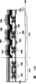
Another mechanism relates to the process of building heterostructure (that is, forming organic interface).Organic light-emitting devices with heterostructure is made by that multichamber type (in line style) evaporation equipment as shown in Figure 2 usually, so that avoid polluting when forming equivalent layer.
Be an evaporation equipment that is used to form double-heterostructure as example shown in Fig. 2 of conceptual schematic view, described double-heterostructure is made up of hole transfer layer, light-emitting layer and electron transfer layer.First light, the substrate with anode (for example by indium tin oxide (after this being called as ITO)) is introduced into feed compartment. at the indoor ultraviolet irradiation substrate that under vacuum atmosphere, utilizes of ultraviolet irradiation with the cleaning anode surface.Especially when anode be during as ito anode, in pretreatment chamber, to carry out oxidation processes.So the level of layer structure is formed.The hole transfer layer is formed in vaporization chamber 201, and light-emitting layer in vaporization chamber 202 to 204 (the red, green and blue layer in Fig. 2) is formed, and is formed at vaporization chamber 205 electron transfer layers.Negative electrode is formed by the evaporation in the vaporization chamber 206. and last, in closed chamber, seal and from discharge chamber, take out substrate, so that obtain organic light-emitting devices.Reference symbol 215 to 216 expression evaporation sources.
So online type evaporation equipment is characterised in that different layers is formed by the evaporation in different chamber 201 to 205.In other words this equipment so is configured to, so that the mixing of each layer material is almost completely avoided.
Though be lowered to 10 usually in the evaporation equipment pressure inside
-4To 10
-5Pascal, but still have the gas componant (for example oxygen and steam) of small quantity.Allegedly have under the vacuum degree of this degree, the gas componant of these small quantities in seconds is easy to form monomolecular adsorption layer.
Thereby when utilizing device fabrication shown in Figure 2 to have the organic light-emitting devices of layer structure, problem is the time interval long between the formation of the formation of a layer and another layer.In order at large to set forth, the undesirable adsorption layer that is caused by the gas componant (after this being called as impurity layer) of small quantity may form in the time interval between cambium layer, especially when substrate is transmitted through second transfer chamber.
One of them concept nature signal as shown in Figure 3.In Fig. 3, in the time of above the second layer is placed to ground floor, by first organic compound, 301 formed ground floors 311 and between by second organic compound, the 302 formed second layers 312, impurity layer 313 is formed by the impurity 303 (as steam or oxygen) of small quantity.
When impurity layer by this way when (promptly at the organic interface place) forms between these layers, it serves as extrinsic region, when organic light emitting devices is done, this areas captured charge carrier, thereby stop the motion of charge carrier. therefore, thereby driving voltage may be raised and reduce the light emission effciency. in addition, the existence of catching the extrinsic region of charge carrier causes the accumulation of electric charge, thereby may impel above-mentioned brightness to reduce.
In order to solve the problems referred to above (form that degenerates of organic interface and the formation of impurity layer) that occur in the organic interface place, the present inventor has designed connected structure as shown in Figure 4.
Fig. 4 is by the sectional drawing of zone 411, zone 412 and the organic compound film formed of Mixed Zone 413. and regional 411 are made up of micromolecule 401.Zone 412 is made up of big molecule 402. Mixed Zone 413 comprise micromolecule 401 and big molecule 402 the two. obviously from Fig. 4 as seen in Fig. 1, do not have organic interface 113, do not have bad consistency zone 114 yet.Thereby this problem of degradation form of organic interface can be solved.
It is very simple and apparent how to solve the problem that forms impurity layer.When connected structure as shown in Figure 4 is manufactured when coming out, the zone of micromolecule 401 411 is formed by evaporation, and is deposited in addition by the big molecule 402 of co-evaporated and forms Mixed Zone 413.After Mixed Zone 413 was done, the deposit of the micromolecule 401 that causes by evaporation is ended and only had by what evaporation caused macromolecularly was deposited on continuation. and this causes one or both materials not formed the situation of organic interface by deposit continuously by evaporation.Thereby, adopt evaporation equipment as shown in Figure 2 not exist in the time interval that exists usually when making organic light-emitting devices.In brief, there is not the time that allows to form impurity layer.
By utilizing such connected structure, do not form organic interface, thereby the motion of charge carrier is unaffected in light emission effciency and useful life steady and organic light-emitting devices.In addition, the same in traditional layer structure that coexists, the function separation is guaranteed.
Contrast with the traditional layer structure that only is different material easy engagement (heterojunction), connected structure of the present invention can be called as the knot of mixing, and it can provide a kind of organic light-emitting devices based on novel concept.
So adopt this viewpoint, the present inventor has further designed scheme and has obtained indigo plant or white organic light-emitting devices, organic interface in this device laminate structure is cancelled basically, and these layers show transmission charge carrier and radiative function separately simultaneously.
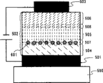
Fig. 5 A and Fig. 5 B are the conceptual schematic view that is incorporated into the blue organic light-emitting devices that double-heterostructure obtains by the knot that will mix.Though anode 501 is placed on the substrate 500 at this, structure can be reversed into negative electrode 503 and is placed on the substrate.By 502 expressions are organic compound films.
Device among Fig. 5 A has by the formed hole of hole material for transfer transport zone 504, by the formed light emitting area 505 of blue light emitting material and by the formed electron transfer of electron transfer material zone 506.As a feature of the present invention, this device also is equipped with the first mixed Mixed Zone 507 of wherein hole material for transfer and blue light emitting material and wherein electron transfer material and the second mixed Mixed Zone 508 of blue light emitting material.
Device among Fig. 5 B has by the formed hole of hole material for transfer transport zone 514, by blue light emitting material 519 being doped to the light emitting area 515 that obtains on the host material, and by the formed electron transfer of electron transfer material zone 516.As a feature of the present invention, this device also is equipped with the first mixed Mixed Zone 517 of wherein hole material for transfer and host material and wherein electron transfer material and the second mixed Mixed Zone 518 of host material.
Fig. 6 A and Fig. 6 B are the conceptual schematic view that is incorporated into the white organic light-emitting devices that double-heterostructure obtains by the knot that will mix.Though anode 501 is placed on the substrate 500 at this, structure can be reversed into negative electrode 503 and is placed on the substrate.By 502 expressions are organic compound thin film.
Device among Fig. 6 A has by the formed hole of hole material for transfer transport zone 504, by the formed light emitting area 505 of blue light emitting material and by the formed electron transfer of electron transfer material zone 506.As a feature of the present invention, this device also is equipped with the first mixed Mixed Zone 507 of wherein hole material for transfer and blue light emitting material and wherein electron transfer material and the second mixed Mixed Zone 508 of blue light emitting material.In order to make this device emission white light, be doped second light-emitting material 601 by blue light emitting material formed regional 505, this material emission has than blue light long wavelength's light more.From the preferred colors of second light-emitting material, 601 emissions is yellow to crocus basically.
Be partly rather than fully to be doped with second light-emitting material 601 as desired by blue light emitting material formed regional 505.This is because in order to obtain white light, also must be removed from the blue light of blue light emitting material.
Another selection of Fig. 6 A is that Mixed Zone 507 or 508 is doped with second light-emitting material 601.As its a example, Fig. 6 B is depicted as the device that first Mixed Zone 507 wherein is doped second light-emitting material.
Having introduced the knot that mixes therein also can adopt second light-emitting material and the 3rd light-emitting material as dopant except blue light emitting material to the white organic light-emitting devices of double-heterostructure.Second light-emitting material emission has that more long wavelength's light and the emission of the 3rd light-emitting material have more long wavelength's light of the light launched than second light-emitting material than blue light. consider the three primary colors of light, preferably second light-emitting material and the 3rd light-emitting material transmitting green light and ruddiness respectively.
In this case, being second light-emitting material ideally is used to be doped to different Mixed Zone (that is, first Mixed Zone be doped a kind of material and second Mixed Zone has been doped another kind of material) with the 3rd light-emitting material.In example shown in Figure 7, first Mixed Zone 507 has been doped second light-emitting material 701 and second Mixed Zone 508 has been doped the 3rd light-emitting material 702.
Relate to by the knot that will mix by the end of present explanation and to be incorporated into the apparatus structure that double-heterostructure obtains.Following be noted that is incorporated into the apparatus structure that the single heterojunction structure obtains by the knot that will mix.Fig. 8 A and Fig. 8 B are the conceptual schematic view that is incorporated into the blue organic light-emitting devices that the single heterojunction structure obtains by the knot that will mix.Though be placed on the substrate 800 at this anode 801, structure can be reversed into negative electrode 803 and is placed on the substrate.By 802 expressions are organic compound films.
Device among Fig. 8 A has by the formed hole of hole material for transfer transport zone 804 and by the formed electron transfer of electron transfer material zone 805.As a feature of the present invention, this device also is equipped with wherein hole material for transfer and the mixed Mixed Zone 806 of electron transfer material.Hole material for transfer or electron transfer material emission blue light.
Device among Fig. 8 B has by the formed hole of hole material for transfer transport zone 804 and by the formed electron transfer of electron transfer material zone 805.As a feature of the present invention, this device also is equipped with wherein hole material for transfer and the mixed Mixed Zone 806 of electron transfer material.This Mixed Zone 806 has been doped blue light emitting material 807.
Fig. 9 A and Fig. 9 B are the conceptual schematic view that is incorporated into the white organic light-emitting devices that the single heterojunction structure obtains by the knot that will mix.Though be placed on the substrate 800 at this anode 801, structure can be reversed into negative electrode 803 and is placed on this substrate.By 802 expressions are organic compound films.
Device among Fig. 9 A has by the formed hole of hole material for transfer transport zone 804 and by the formed electron transfer of electron transfer material zone 805.As a feature of the present invention, this device also is equipped with wherein hole material for transfer and the mixed Mixed Zone 806 of electron transfer material.Hole material for transfer or electron transfer material emission blue light.In order to make this device emission white light, be doped second light-emitting material 901 by blue light emitting material formed regional 806, this material emission has than blue light long wavelength's light more.From the preferred colors of second light-emitting material, 901 emissions is yellow to crocus basically.
Be as desired, this is because in order to obtain white light partly rather than fully to be doped with second light-emitting material 901. by blue light emitting material formed regional 805, also must be removed from the blue light of blue light emitting material emission.
Another selection of Fig. 9 A is that hole transport zone 804 or electron transfer zone 805 are doped with second light-emitting material 901.As its a example, Fig. 9 B is depicted as the device that electron transfer zone 805 wherein is doped second light-emitting material.
The white organic light-emitting devices that obtains by the knot of introducing mixing also can adopt second light-emitting material and the 3rd light-emitting material as dopant except blue light emitting material.Second light-emitting material emission has that more long wavelength's light and the emission of the 3rd light-emitting material have more long wavelength's light of the light launched than second light-emitting material than blue light.Consider the three primary colors of light, preferably second light-emitting material and the 3rd light-emitting material difference transmitting green light and ruddiness.
In this case, being second light-emitting material ideally is used to be doped to different carrier transport zone (that is, hole transport zone be doped a kind of material and the electron transfer zone has been doped another kind of material) with the 3rd light-emitting material.In example shown in Figure 10, hole transport zone 804 has been doped second light-emitting material 1001 and electron transfer zone 805 has been doped the 3rd light-emitting material 1002.
Though in any figure of Fig. 5 A to 10, do not show, may be inserted between anode and the organic compound film by being used to improve material (after this being called as hole-injecting material) the formed hole injection zone that injects in the hole.Equally, may be inserted between negative electrode and the organic compound film by being used to improve material (after this being called as the electronics injection material) the formed electron injection region territory that electronics injects.
Hole-injecting material and electronics injection material have the reduction charge carrier and are injected into the ability that organic compound film is hampered and keeps off from electroplax.Thereby hole injection zone and electron injection region territory have makes the motion of charge carrier from the electrode to the organic compound thin film steadily to prevent the effect of electric charge accumulation.For fear of forming aforesaid impurity layer, under not free situation at interval before or after the organic compound, injection material is formed film.
Above-mentioned indigo plant or white organic light-emitting devices can be obtained high light emission effciency and long useful life.Therefore, by this organic light-emitting devices is combined with CCM method or CF method, can obtain a kind of full color display, it has the light emission effciency higher than traditional display unit, longer useful life and better productivity ratio.
Brief description of drawings
In appended accompanying drawing:
Figure 1 shows that the state diagram of an organic interface.
Figure 2 shows that evaporation equipment figure.
Figure 3 shows that the formation figure of impurity layer.
Figure 4 shows that the state diagram of mixed zone.
Fig. 5 A and 5B are depicted as the structure chart of blue organic light-emitting devices.
Fig. 6 A and 6B are depicted as the structure chart of white organic light-emitting devices.
Figure 7 shows that a kind of structure chart of white organic light-emitting devices.
Fig. 8 A and 8B are depicted as the structure chart of blue organic light-emitting devices.
Fig. 9 A and 9B are depicted as the structure chart of white organic light-emitting devices.
Figure 10 shows that a kind of structure chart of white organic light-emitting devices.
Figure 11 shows that evaporation equipment figure.
Be respectively display unit that adopts color conversion layer and the schematic diagram that adopts the display unit of colour filter shown in Figure 12 A and the 12B.
Figure 13 A and 13B are depicted as the cross-section structure of display unit.
Figure 14 shows that a kind of cross-section structure of display unit.
Be respectively superstructure and its cross-section structure of display unit shown in Figure 15 A and the 15B.
Figure 16 shows that a kind of cross-section structure of display unit.
Figure 17 A to 17C is depicted as display unit figure, and wherein Figure 17 A is depicted as its superstructure and Figure 17 B and 17C and is depicted as its section structure.
Figure 18 A and 18B are depicted as the structure chart of display unit.
Figure 19 A and 19B are depicted as the structure chart of display unit.
Figure 20 A to 20C is depicted as the structure chart of display unit.
Figure 21 A to 21F is depicted as the instantiation figure of electrical equipment.
Figure 22 A and 22B are depicted as the instantiation figure of electrical equipment.
Shown in Figure 23 is the structure chart of display unit; And
Shown in Figure 24 is the evaporation source of concrete organic compound.
Detailed description of preferred embodiments
Implementing pattern of the present invention will be illustrated below.Generally, if the male or female of organic light-emitting devices is transparent in to take out the light of being launched, then this is enough.In the organic light-emitting devices of this embodiment pattern, on substrate, form transparent anode so that light is taken out by anode.Yet the present invention also is applicable to other structure and can forms negative electrode on substrate so that by negative electrode light taking-up or light can be removed from the opposite of substrate.
When implementation was of the present invention, the process of making organic light-emitting devices must be carried out design to avoid the formation of impurity layer.Therefore a kind of method of organic light-emitting devices constructed in accordance at first is described.
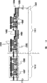
Figure 11 A is the top view of evaporation equipment.This equipment is the single chamber form, is configured to vaporization chamber and has a plurality of evaporation sources in vacuum tank at this indoor vacuum tank 1110.In a plurality of evaporation sources, storing material respectively, as hole-injecting material, hole material for transfer, electron transfer material, electronics injection material, barrier material, light-emitting material be used to form the material of negative electrode with difference in functionality.
In having the evaporation equipment of this vaporization chamber, have anode (by ITO or similar formation) if substrate be introduced into feed compartment. anode is a kind of oxide such as ITO, then oxidation processes is carried out (though do not express, evaporation equipment can be equipped with the ultraviolet irradiation chamber with the cleaning anode surface) in Figure 11 A in pretreatment chamber.All materials that constitute organic light-emitting devices all will stand evaporation in vacuum tank 1110.Negative electrode can be formed in vacuum tank 1110, perhaps can be formed in independent vaporization chamber.Briefly, if the layer of negative electrode front forms by evaporation in vacuum tank 1110, then this is enough.At last, in closed chamber, seal and substrate is removed in discharge chamber to obtain organic light-emitting devices.
The program that adopts the evaporation equipment of this single chamber form to make organic light-emitting devices of the present invention is illustrated with reference to Figure 11 B (sectional drawing of vacuum tank 1110).Is to utilize the vacuum chamber 1110 with three evaporation sources (organic compound evaporation source a1116, organic compound evaporation source b1117 and organic compound evaporation source c1118) to form the process of organic compound films (organic compound thin film 502 shown in Fig. 5 A) as a simplified example shown in Figure 11 B, and this organic compound film comprises hole material for transfer 1121, electron transfer material 1122 and blue light emitting material 1123.
At first, the substrate 1101 with anode 1102 is introduced into vacuum tank 1110 and fixes (usually, substrate is rotated during evaporating) by fixed pedestal 1111.Secondly, the pressure in the vacuum tank 1110 is lowered and (is preferably 10
-4Pascal or lower) and subsequently container a1112 be heated with evaporation hole material for transfer 1121. when reach given evaporation rate (unit:
 ) time, flashboard a 1114 is opened with start vaporizer.
After hole transport zone 1103 reaches given thickness, the evaporation of blue light emitting material 1123 be activated and meanwhile hole material for transfer 1121 be evaporated to form first Mixed Zone 1105 (corresponding to the state shown in Figure 11 B) always.Flashboard a 1114 is fully closed the light emitting area that comprises blue light emitting material 1123 with the evaporation that finishes hole material for transfer 1121 and formation then.At this moment, container b 1113 is heated under flashboard b 1115 pent situations.
After light emitting area reaches a given thickness, flashboard b 1115 is opened and the evaporation of electron transfer material 1122 is activated to form second Mixed Zone. and last, the evaporation of blue light emitting material 1123 finishes and comprises that the electron transfer zone of electron transfer material 1122 is formed. and all aforesaid operations carry out under without any the situation in the time interval in succession, therefore all do not have the formation of impurity layer in any zone.
The concrete shape of organic compound evaporation source a 1116, organic compound evaporation source b 1117 and organic compound evaporation source c 1118 as shown in figure 24.Have and adopted cell (cell) under a kind of situation or adopted the conduction heater, and adopt the situation of conduction heater in Figure 24, to be shown.Briefly, container a 1112, container b 1113 and container c 2411 constitutes the conduction heaters, and comprise hole material for transfer 1121 container a 1112, comprise electron transfer material 1122 container b 1113, comprise that the container c 2411 of blue light emitting material is clipped in the middle by electrode a 2401, electrode b 2402 and electrode c 2403 respectively.Then, container a 1112, container b 1113 and container c 2411 are by the streaming current heating evaporation.The flashboard c 2412 that is used for organic compound evaporation source c 1118 also is shown at this.
All organic light-emitting devices that illustrate in " summary of the invention " can be made by using this method.For example, comprise blue light emitting material as with respect to the equipment of the material of living away from home of host material the time making shown in Fig. 5 B, the evaporation source that is used for evaporating host material can be added to the element of Figure 11 B.Host material is used to form the Mixed Zone and forms light emitting area, and is evaporated so that be entrained on the host material with small quantity at (during forming light emitting area) light-emitting material during the evaporation host material.
Under the situation about being formed in hole injection zone or electron injection region territory, the evaporation source of every kind of injection material is placed in the same vacuum tank 1110.For example, if the hole injection zone is formed between anode 1102 and hole transport zone 1103 by evaporation in Figure 11 B, then after hole-injecting material is deposited on anode 1102 by evaporation under the situation without any the time interval, hole material for transfer 1121 just is evaporated immediately.Avoided the formation of impurity thus.
Below cited be preferable material as hole-injecting material, hole material for transfer, electron transfer material, electronics injection material and light-emitting material.But the material that can be used for organic light-emitting devices of the present invention is not restricted to this.
For hole-injecting material, in the boundary line of organic compound, especially phthalocyanine (after this is called as H
2Pc) based compound, copper phthalocyanine (after this being called as CuPc) are often used.In condensate, can be used by in the conjugated system conductive polymer, carrying out the material that chemical doping obtains.These polymeric examples comprise the polyethylene dioxy base thiophene (after this polyethylene dioxythiophene is called as PEDOT) that is doped with polystyrolsulfon acid (after this being called as PSS) and are doped with iodine or the polyaniline or the polypyrrole of other lewis acid (Lewis acid).Condensate as insulator also is effectively with regard to anode planesization, and often adopts polyimides (after this being called as PI).Effectively hole-injecting material can find in inorganic compound that also the example comprises the film of gold, platinum or other metalloid and the extremely thin film of aluminum oxide (after this being called as aluminium oxide).
As the widely used material of hole material for transfer is aromatic amino (aromatic amine-based) (that is, those have phenyl ring-nitrogen key) compound.Wherein, what especially be widely used is: 4,4 '-it is two that (hexichol amido)-biphenyl is (after this, TAD); Its derivative, promptly 4,4 '-it is two that [N-(3-aminomethyl phenyl)-N-phenyl-amido]-biphenyl is (after this, TPD); And 4,4 '-two-[N-(1-naphthyl)-N-phenyl-amido]-biphenyl (α-NPD) after this. what also be used has a star burst aromatic amine compound, comprising: 4,4 ', 4 "-three (N, N-diphenyl-amido)-triphenylamine is (after this, TDATA); And 4,4 ', 4 "-three [N-(3-aminomethyl phenyl)-N-phenyl-amido]-triphenylamine (after this, MTDATA).
Metal complex is through being often used as electron transfer material.Example wherein comprises: have the metal complex of quinoline backbone or benzoquinoline backbone, Alq as the aforementioned, three (4-methyl-8-quinolinolate) aluminium (after this, Almq) and two (10-hydroxy benzos [h]-quinolinolate) beryllium (after this, Bebq); And be that (2-methyl-8-quinolinolate)-(4-hydroxyl-xenyl)-aluminium (after this for a kind of ligand complex two of mixing, BAlq). example comprises that also tool has the metal complex of oxazolyl and thiazolyl ligand, as two [2-(2-hydroxyphenyl)-benzoxazoles] zinc (Zn (BOX) after this,
2) and two [2-(2-hydroxyphenyl)-benzothiazole] zinc (Zn (BTZ) after this,
2). having other material higher than metal complex metastatic electron ability is: oxadiazole derivative such as 2-(4-xenyl)-5-(4-tert-butyl-phenyl)-1,3, and the 4-oxadiazole is (after this, PBD) and 1, two [5 (the p-tert-butyl-phenyls)-1,3 of 3-, 4-oxadiazole-2-i1] benzene is (after this, OXD-7); Triazole derivative such as 3-(4-tert-butyl-phenyl) 4-phenyl-5-(4-xenyl)--1,2, (after this, TAZ) and 3-(4-tert-butyl-phenyl)-4-(4-ethylphenyl)-5-(4-xenyl)-1,2, the 4-triazole is (after this, p-EtTAZ) for the 4-triazole; And phenanthroline derivative such as bathophenanthroline (after this, BPhen) and bathocuproin (after this, BCP).
Above given electron transfer can be used as the electronics injection material.In addition, extremely thin insulator film comprises that the metal halide of alkalescence such as the metal oxide such as the lithia of lithium fluoride and alkalescence often are used.Alkalinous metal complex such as acetylacetone,2,4-pentanedione lithium (lithium acetylacetonate) (Li (acac) after this) and 8-quinolinolate-lithium (Liq) also be effective after this.
Except above-mentioned Alq, Almq, BeBq, BAlq, the Zn (BOX) of comprising
2And Zn (BTZ)
2Metal complex beyond, can be various fluorescent pigments as the material of effective light-emitting material.The example of fluorescent pigment is included as 4,4 ' blue-two (2,2-biphenyl-vinyl)-biphenyl (after this, DPVBi) and (p-dimethylamino styryl)-the 4H-pyrans (after this, DCM) for the 4-of reddish orange (dicyano methylene)-2-methyl-6-.Ternary light-emitting material also can be used and its main flow is to have platinum or the iridium complex as important meals. and known ternary light-emitting material comprises three (2-phenylpyridine) iridium (Ir (ppy) after this,
3) and 2,3,7,8,12,13,17,18-octaethyl-21H, 23H-porphyrin-platinum (after this, PtOEP).
Have that the above-mentioned material of corresponding function is combined forms organic light-emitting devices of the present invention, have whereby than the higher smooth emission effciency of conventional apparatus and more the organic light-emitting devices of long life can be manufactured come out.
Such organic light-emitting devices be used to make full color display and Figure 12 A and 12B each all schematically demonstrate the structure of thus obtained display unit.Figure 12 A has shown the CCM method, and its medium blue organic light-emitting devices combines with color conversion layer.Figure 12 B has shown the CF method, and wherein white organic light-emitting devices combines with colour filter.In Figure 12 A, the color conversion layer of B → B is always necessary.
[embodiment 1]
This embodiment demonstrates an instantiation of device, and this device has this spline structure, in this structure the hole injection zone be inserted in Fig. 5 A between the anode 501 and organic compound film 502 in the illustrational blue organic light-emitting devices.
At first, be deposited to the thickness of about 100 nanometers so that on glass substrate 500, form anode 501 by sputtering ITO.The glass substrate 500 that has an anode 501 is introduced into the vacuum tank shown in Figure 11 A and 11B.In this embodiment, in order to be necessary by five evaporation sources of five kinds of materials of evaporation deposition (four kinds of organic compounds and a kind of metal that forms negative electrode).
At first, be deposited to the thickness of 20 nanometers so that form the hole injection zone as the MTDATA of hole-injecting material by evaporation. when the evaporation that reaches 20 nanometers and MTDATA when film thickness is terminated, as the evaporation of the spiral shell dimer (spiro dimer) (after this being called as S-TAD) of the TAD of hole material for transfer immediately with
 Evaporation rate be activated.Do not allow the time interval to avoid the formation of aforesaid impurity at this.
The hole transport zone 504 that includes only S-TAD with
 Evaporation rate be formed into the thickness of 20 nanometers after, when keeping the S-TAD evaporation rate, as the evaporation of the spiral shell dimer (spiro dimer) (after this being called as S-DPVBi) of the DPVBi of light-emitting material with
Evaporation rate be activated. therefore formed first
Evaporation rate be formed into the thickness of 20 nanometers after, when keeping the S-TAD evaporation rate, as the evaporation of the spiral shell dimer (spiro dimer) (after this being called as S-DPVBi) of the DPVBi of light-emitting material with
Evaporation rate be activated. therefore formed first Mixed Zone 507 by co-evaporated, wherein the ratio of S-TAD and S-DPVBi is 1:1.The thickness in zone 507 is set to 10 nanometers.
In first Mixed Zone 507 was formed, the evaporation of S-TAD was terminated and the evaporation of S-DPVBi is continuing to form light emitting area 505.Light emitting area will have the thickness of 20 nanometers.Subsequently, along with the evaporation of S-DPVBi is continuing, as the evaporation of the Alq of electron transfer material with
 Evaporation rate be activated.Formed second
 Mixed Zone 508 by co-evaporated thus, the ratio of S-DPVBi and Alq is 1:1 in this zone.The thickness in zone 508 is set to 10 nanometers.
In second Mixed Zone 508 was formed, the evaporation of S-DPVBi was terminated and the evaporation of Alq is that the electron transfer zone 506. of 40 nanometers is last continuing to have thickness with formation, is about 400 nanometers as negative electrode 503 by the evaporation deposition ytterbium to thickness.The blue organic light-emitting devices that is derived from S-DPVBi obtains therefrom.
[embodiment 2]
This embodiment demonstrates an instantiation of device, and this device has this spline structure, in this structure the electron injection region territory be inserted in Fig. 5 B between the negative electrode 513 and organic compound film 512 in the illustrational blue organic light-emitting devices.
At first, be deposited to the thickness of about 100 nanometers so that on glass substrate 510, form anode 511 by sputtering method ITO.The glass substrate 510 that has an anode 511 is introduced into the vacuum tank shown in Figure 11 A and 11B. in this embodiment, and in order to be necessary by six evaporation sources of six kinds of materials of evaporation deposition (five kinds of organic compounds and a kind of metal that forms negative electrode).
At first, the hole transport zone 514 that includes only TPD is formed into the thickness of 30 nanometers. then keep TPD with
 Evaporation rate the time, as the evaporation of the BAlq of light-emitting material host material also with
 Evaporation rate be activated. in other words, comprise that the city, first
 mixed zone 517 by 1:1 percentage of T PD and BAlq is formed by co-evaporated. the thickness of first area 517 is 10 nanometers.
When first Mixed Zone 517 is formed, the evaporation of TPD is terminated and thickness that the evaporation of BAlq is continuing to form light emitting area 515. light emitting areas always is 20 nanometers. at this moment, light emitting area 515 is doped the perylene (perylene) of 5wt%, and perylene is the blue fluorescent pigment as light-emitting material 519.
When light emitting area 515 finished, the evaporation of perylene was terminated and the evaporation of Balq is still continuing. meanwhile, as the evaporation of the Alq of electron transfer material with
 Evaporation rate be activated. in other words, comprise that second
 Mixed Zone 518 in the BAlq of 1:1 ratio and Alq is formed by evaporation. the thickness of second Mixed Zone is 10 nanometers.
When finish second Mixed Zone 518, the evaporation of BAlq be terminated and the evaporation of Alq continue with formation have thickness be 30 nanometers electron transfer zone 516. in addition, be formed as the Li (acac) of electronics injection material that to have thickness be that the film of 2 nanometers is with as the electron injection region territory.
At last, being deposited to the thickness of about 150 nanometers as negative electrode by evaporation aluminium. the blue organic light-emitting devices that is derived from perylene obtains therefrom.
[embodiment 3]
The present embodiment demonstrate as Fig. 6 A an instantiation of illustrational white organic light-emitting devices.
At first, be deposited to the thickness of about 100 nanometers by sputtering method ITO and be introduced into vacuum tank shown in Figure 11 A and 11B so that on glass substrate 500, form glass substrate 500 that anode 501. has anode 501. in this embodiment, in order to be necessary by five evaporation sources of five kinds of materials of evaporation deposition (four kinds of organic compounds and a kind of metal that forms negative electrode).
At first, the hole transport zone 504 that includes only α-NPD is formed into the thickness of 30 nanometers. then, keep α-NPD with
 Evaporation rate the time, as the Zn (BTZ) of blue light emitting material (in fact this color is the Bluish white whiter than blueness)
2Evaporation with
Evaporation rate the time, as the Zn (BTZ) of blue light emitting material (in fact this color is the Bluish white whiter than blueness)
2Evaporation with
 Evaporation rate be activated. in other words, comprise α-NPD and Zn (BTZ) in the 1:1 ratio
2First
Evaporation rate be activated. in other words, comprise α-NPD and Zn (BTZ) in the 1:1 ratio
2First Mixed Zone 507 be formed by co-evaporated. the thickness of first area 507 is 10 nanometers.
When finished first Mixed Zone 507, the evaporation of α-NPD was terminated and Zn (BTZ)
2The thickness that always continuing to form light emitting area 505. light emitting areas of evaporation be 20 nanometers.At this moment, last 10 nanometers of light emitting area 505 (promptly between thickness is 10 nanometers and 20 nanometer height on the light emitting area of 20 nanometers) are doped weight and account for 5% DCM, and DCM is the reddish orange fluorescent pigment as second light-emitting material 601.
When light emitting area 505 finished, the evaporation of DCM is terminated and Zn (BTZ)
2Evaporation still continuing. meanwhile, as the evaporation of the BAlq of electron transfer material with
 Evaporation rate be activated. in other words, comprise Zn (BTZ) in the 1:1 ratio
2Be formed by evaporation with second
Evaporation rate be activated. in other words, comprise Zn (BTZ) in the 1:1 ratio
2Be formed by evaporation with second Mixed Zone 508 of BAlq.The thickness of second Mixed Zone is 10 nanometers.
When finish second Mixed Zone 508, Zn (BTZ)
2Evaporation be terminated and the evaporation of BAlq is continuing to have the electron transfer zone 506 that thickness is 30 nanometers with formation.At last, aluminium: lithium alloy is deposited to the thickness of about 150 nanometers as negative electrode by evaporation. and white organic light-emitting devices obtains therefrom.
[embodiment 4]
The present embodiment demonstrate as Fig. 7 an instantiation of illustrational white organic light-emitting devices.
At first, be deposited to the thickness of about 100 nanometers by sputtering method ITO and be introduced into vacuum tank shown in Figure 11 A and 11B so that on glass substrate 500, form glass substrate 500 that anode 501. has anode 501.In this embodiment, in order to be necessary by six evaporation sources of six kinds of materials of evaporation deposition (five kinds of organic compounds and a kind of metal that forms negative electrode).
At first, the hole transport zone 504 that includes only α-NPD is formed into the thickness of 30 nanometers. then, keep α-NPD with
 Evaporation rate the time, as the evaporation of the S-DPVBi of blue light emitting material also with
 Evaporation rate be activated. in other words, comprise that with regard to evaporation rate first
 Mixed Zone 507 in the α-NPD of 1:1 ratio and S-DPVBi is formed by co-evaporated.The thickness of first Mixed Zone is 10 nanometers.At this moment, add weight and account for 0.5% N, N '-dimethylquinacridone (being called as " Dmq ") is as second light-emitting material 701, and it is a green fluorescence pigment.
When finished first Mixed Zone 507, the evaporation of α-NPD was terminated and the evaporation of S-DPVBi is continuing to form light emitting area 505.The thickness of light emitting area is 20 nanometers.Then, as the evaporation of the Alq of electron transfer material with
 Evaporation rate be activated, continue the evaporation of S-DPVBi simultaneously.Formed by co-evaporated thus is second
 Mixed Zone 508, and the ratio of S-DPVBi and Alq is 1:1 with regard to evaporation rate in this Mixed Zone.The thickness in zone 508 is set to 10 nanometers.At this moment, weight accounts for 0.5% and is added to this zone as the 3rd light-emitting material 702 for the DCM of reddish orange fluorescent pigment.
When finished second Mixed Zone 508, the evaporation of S-DPVBi was terminated and the evaporation of Alq is continuing to have the electron transfer zone 506 that thickness is 30 nanometers with formation.At last, aluminium: lithium alloy is deposited to the thickness of about 150 nanometers as negative electrode by evaporation.White organic light-emitting devices obtains therefrom.
[embodiment 5]
This embodiment demonstrates an instantiation of device, and this device has this spline structure, in this structure the electron injection region territory be inserted in Fig. 8 A between the negative electrode 803 and organic compound film 802 in the illustrational blue organic light-emitting devices.
At first, be deposited to the thickness of about 100 nanometers so that on glass substrate 800, form anode 801 by sputtering method ITO.The glass substrate 800 that has an anode 801 is introduced into the vacuum tank shown in Figure 11 A and 11B.In this embodiment, in order to be necessary by four evaporation sources of four kinds of materials of evaporation deposition (three kinds of organic compounds and a kind of metal that forms negative electrode).
At first, the hole transport zone 804 that includes only α-NPD with
 Evaporation rate be formed into after the thickness of 40 nanometers, keep α-NPD with
 Evaporation rate the time, as the evaporation of the BCP of electron transfer material also with
 Evaporation rate be activated.Formed by co-evaporated thus is
 Mixed Zone 806, and the ratio of α-NPD and BCP is 1:1 with regard to evaporation rate in this Mixed Zone 806.The thickness in zone 806 is set to 20 nanometers.
806 when finishing in the Mixed Zone, and the evaporation of α-NPD is terminated and the evaporation of BCP is the electron transfer zone 805 of 20 nanometers continuing to form thickness.In addition, being activated to form thickness under the situation in the no time interval as the evaporation of the Alq of electronics injection material is the electron injection region territory of 40 nanometers.
At last, aluminium: lithium alloy is deposited to the thickness of about 150 nanometers as negative electrode 803 by evaporation.The blue organic light-emitting devices that is derived from α-NPD obtains therefrom.Attention: if blue fluorescent pigment such as perylene are added to Mixed Zone 806, then the form shown in Fig. 8 B is possible.
[embodiment 6]
The present embodiment demonstrate as Fig. 9 B an instantiation of illustrational white organic light-emitting devices.
At first, ITO is deposited to the thickness of about 100 nanometers so that form anode 801 on glass substrate 800 by sputtering method.The glass substrate 800 that has an anode 801 is introduced into the vacuum tank shown in Figure 11 A and 11B. in this embodiment, and in order to be necessary by four evaporation sources of four kinds of materials of evaporation deposition (three kinds of organic compounds and a kind of metal that forms negative electrode).At first, the hole transport zone 804 that includes only α-NPD with
 Evaporation rate be formed into after the thickness of 40 nanometers, when keeping the evaporation rate of α-NPD, as the evaporation of the BAlq of electron transfer material also with
 Evaporation rate be activated.Formed by co-evaporated thus is
 Mixed Zone 806, and the ratio of α-NPD and BAlq is 1:1 with regard to evaporation rate in this Mixed Zone 806.The thickness in zone 806 is set to 20 nanometers.
806 when finishing in the Mixed Zone, the evaporation of α-NPD be terminated and the evaporation of BAlq to continue with formation thickness be the electron transfer zone 805 of 40 nanometers always.At this moment, preceding 10 nanometers in electron transfer zone 805 (promptly between thickness is 0 nanometer and 10 nanometer height on the electron transfer zone of 40 nanometers) are doped weight and account for 5% rubrene, and rubrene is the yellow fluorescence pigment as second light-emitting material 901.
At last, aluminium: lithium alloy is deposited to the thickness of about 150 nanometers as negative electrode 803 by evaporation.White organic light-emitting devices obtains therefrom.
[embodiment 7]
The present embodiment demonstrate as Figure 10 an instantiation of illustrational white organic light-emitting devices.
At first, be deposited to the thickness of about 100 nanometers by sputtering method ITO and be introduced into vacuum tank shown in Figure 11 A and 11B so that on glass substrate 800, form glass substrate 800 that anode 801. has anode 801.In this embodiment, in order to be necessary by five evaporation sources of five kinds of materials of evaporation deposition (four kinds of organic compounds and a kind of metal that forms negative electrode).
At first, the hole transport zone 804 that includes only α-NPD with
 Evaporation rate be formed into the thickness of 40 nanometers.At this moment, last 10 nanometers in electron transfer zone 804 (promptly between thickness is 30 nanometers and 40 nanometer height on the hole transport zone of 40 nanometers) are doped weight and account for 5% DMq, and DMq is the green fluorescence pigment as second light-emitting material 1001.
Secondly, after hole transport zone 804 is formed, in the evaporation rate that keeps α-NPD, as the evaporation of the BAlq of electron transfer material also with
 Evaporation rate be activated.Formed by co-evaporated thus is
 Mixed Zone 806, and the ratio of α-NPD and BAlq is 1:1 with regard to evaporation rate in this Mixed Zone 806.The thickness in zone 806 is set to 30 nanometers.
After finish Mixed Zone 806, the evaporation of α-NPD be terminated and the evaporation of BAlq to continue with formation thickness be the electron transfer zone 805 of 40 nanometers always.At this moment, preceding 10 nanometers in electron transfer zone 805 (promptly between thickness is 0 nanometer and 10 nanometer height on the electron transfer zone of 40 nanometers) are doped weight and account for 5% DCM, and DCM is the reddish orange fluorescent pigment as the 3rd light-emitting material 1002.
At last, aluminium: lithium alloy is deposited to about 150 nanometers by evaporation thickness obtains therefrom as negative electrode 803. white organic light-emitting devices.
[embodiment 8]
This embodiment explanation comprises the display unit according to organic light-emitting devices of the present invention.Figure 13 A and 13B are the sectional drawings that adopts the active matrix display devices of organic light-emitting devices of the present invention.
Be used as active device at this thin-film transistor (after this being called as TFT), but this active device can be a MOS transistor.The TFT of a shown example of conduct is that (planar transistor more specifically), but also can use bottom gate TFT (reverse interleaved typically TFT) to replace to top grid (top gate) TFT.
In Figure 13 A, substrate of 1301 expressions.At this used substrate visible light thoroughly, light is obtained by substrate surface like this.Specifically, glass substrate, quartz substrate, crystal glass or plastic (comprising plastic film) can be used.Substrate 1301 is meant that substrate adds at the formed dielectric film of substrate surface.
On substrate 1301, be equipped with pixel portion 1311 and drive circuit 1312.Pixel portion 1311 will at first be carried out explanation.
Be preferably the p channel TFT at this Current Control TFT 1302.Though also can replace, if Current Control TFT is connected to the anode of organic light-emitting devices shown in Figure 13 A and 13B, then in that to reduce aspect the current drain p channel TFT as Current Control TFT more successful with the n channel TFT.Switching TFT can be n channel TFT or p channel TFT.
The drain electrode of Current Control TFT 1302 is electrically connected to pixel electrode 1303.In this embodiment, have work function and be the material that 4.5 to 5.5eV electric conducting material is used as pixel electrode 1303, therefore, pixel electrode 1303 plays the anode of organic light-emitting devices.The material of transmissive light, typically, the compound of indium oxide, tin oxide, zinc oxide or these oxides (for example, ITO) is used as pixel electrode 1303.Organic compound film 1304 is formed on the pixel electrode 1303.
The layer of being made up of pixel electrode 1303, organic compound film 1304 and negative electrode 1305 is capped layer protecting film 1306.It is in order to protect organic light-emitting devices to avoid oxygen and moisture that diaphragm 1306 is provided.The material that is suitable for diaphragm 1306 comprises silicon nitride, silicon oxynitride, aluminium oxide, tantalum oxide and carbon (particularly, being diamond-like-carbon).
By 1320 expressions is color conversion layer shown in Figure 12 A and the 12B or colour filter.In the example shown here, described layer or colour filter are formed in the indenture that is obtained by processing substrate 1301.When organic compound film 1304 emission blue lights, color conversion layer be used and when organic compound film 1304 is launched white lights colour filter be used.
Secondly, drive circuit 1312 will be carried out explanation.Drive circuit 1312 is zones that are used to control the timing signal (gate signal and data-signal) that is about to be sent to pixel portion 1311, and is equipped with shift register, buffer and latch and analogue quantity switch (transmission gate) or level shifter. the cmos circuit that the elementary cell of these circuit is made up of n channel TFT 1307 and p channel TFT 1308 in Figure 13 A.
Known circuit structure can be applied to shift register, buffer and latch and analog switch (transmission gate) or level shifter.Though pixel portion 1311 is provided on the identical substrate with drive circuit 1312 in Figure 13 A and 13B, IC or LSI can be electrically connected rather than drive circuit 1312 is placed on the substrate.
Pixel electrode in Figure 13 A and 13B (anode) 1303 is electrically connected to Current Control TFT1302, but can change into negative electrode is connected to Current Control TFT.In this case, pixel electrode can be formed by the material of negative electrode 1305, and negative electrode can be formed by the material of pixel electrode (anode) 1303.Current Control TFT is preferably the n channel TFT in this case.
Display unit shown in Figure 13 A is by a kind of technology manufacturing, and the formation of pixel electrode 1303 is prior to the formation of wiring circuit 1309 in this technology.Yet this technology may make the rough surface of pixel electrode 1303. pixel electrode 1303 coarse surfaces may make the characteristics degrade of organic light-emitting devices, because it is the device of a current drives type.
Therefore pixel electrode 1303 can be formed after wiring circuit 1309 forms so that obtain display unit shown in Figure 13 B.In this case, the injection of comparing with the structure of Figure 13 A from the electric current of pixel electrode 1303 improves.
In Figure 13 A and 13B, a preceding taper embankment structure (forward-tapered bankstructure) is if 1310 will to be placed on the pixel of pixel portion 1311 separate. and this embankment structure is reverse taper, then contacting and can be avoided between embankment structure and pixel electrode for example.The example as shown in figure 14.Components identical is represented by identical symbol therewith in Figure 13 A and 13B.
In Figure 14, the wiring circuit also serves as separating part and assigns to form wiring circuit and partitioned portion 1410.In the shape of wiring circuit shown in Figure 14 and partitioned portion 1410 (promptly, structure with cocked bead) can obtain thus, be about to constitute the metal of wiring circuit with than this metal (for example, a kind of metal nitride) layers of material that etch rate is low, the lamination that obtains of etching then.This shape can prevent the short circuit between negative electrode 1405 and pixel electrode 1403 or the wiring circuit.Different with common active matrix display devices, in the device of the negative electrode on the pixel 1405 in Figure 14, be made into bar (similar) with the negative electrode in passive matrix device.
Figure 15 A and 15B are presented at the external form of the active matrix display devices of Figure 13 B illustrated.Figure 15 A is its top view and the sectional drawing got for the P-P ' line in Figure 15 A of Figure 15 B. the symbol among Figure 13 A and the 13B is used to Figure 15 A and 15B.
In Figure 15 A, 1501 remarked pixel parts, the drive circuit of the drive circuit of 1502 expression gate signal sides and 1503 expression data-signal sides.The signal that is about to be sent to the drive circuit 1503 of the drive circuit 1502 of gate signal side and data-signal side is with 1505 to be transfused to through input wires circuit 1504 from TAB (tape automated bonding, tape automated bonding).Though do not show in the drawings, TAB is with 1505 can be replaced by TCP (tape carrierpackage, carrier band encapsulation), and this TCP obtains by IC (integrated circuit) is provided to TAB.
By 1506 represented be coating member, it is provided at the top of the display unit shown in Figure 13 B and bonding by the seal member 1507 that resin constituted.As long as coating member 1506 does not see through the oxygen G﹠W, it can be any material. in this embodiment, shown in Figure 15 B, formed carbon film (diamond-like-carbon particularly) 1506b and 1506c are formed coating member 1506 respectively by plastic components 1506a and in the front surface of plastic components 1506a and rear surface.
Shown in Figure 15 B, the seal member 1508 that is made of resin is stamped in seal member 1507 linings, so that organic light-emitting devices is sealed in the airtight space 1509 fully.Airtight space 1509 can be by inert gas (typically, nitrogen or inactive gas), resin or inert fluid (for example, liquid fluorocarbon, its representative instance is perfluor alkane (perfluoroalkane)) filled. it also is effective putting into adsorbent or deoxidier in described space.
On the display surface (showing face) of the display unit shown in the present embodiment, can be provided with a polarization plates by the image that spectators watched.This polarization plates has the effect that reduces from outside reflection of incident light, thereby prevents that display surface from showing spectators' reflection image.Generally, circularly polarizing plate is used. and still, preferably make polarization plates have the structure of less internal reflection, be reflected and propagate backward in polarization plates with the light that prevents to be launched from organic compound film by regulating refractive index.
Any organic light-emitting devices according to the present invention can be used as the organic light-emitting devices in the display unit that is included in the present embodiment.
[embodiment 9]
The present embodiment shows an active matrix display devices, as an example that comprises according to the display unit of organic light-emitting devices of the present invention. different with embodiment 8, in the display unit of this embodiment, the opposite that only is formed with the substrate of source apparatus from it obtains (after this being called as upwards emission). and Figure 16 is its a sectional drawing.
Be used as active device at this thin-film transistor (after this being called as TFT), but this active device can be a MOS transistor.The TFT of a shown example of conduct be a top grid TFT (planar transistor more specifically), but also can use bottom gate TFT (reverse interleaved typically TFT) replacement.
The substrate 1601 of the present embodiment, be formed in Current Control TFT1602 in the pixel portion 1611 and drive circuit 1612 and the embodiment 8 those and have identical structure.
First electrode 1603 that is connected to Current Control TFT1602 drain electrode is used as anode in the present embodiment, therefore preferably formed by the electric conducting material with big work function. and the typical example of electric conducting material comprises nickel, palladium, tungsten, gold, silver and other metallike mutually.In the present embodiment, be that first electrode 1603 is light tight ideally.Be that electrode is formed by the material of high reflection light even more ideally.
Organic compound film 1604 is formed on first electrode 1603.Second electrode 1605 that provides on organic compound film 1604, second electrode 1605 serves as negative electrode in the present embodiment.Thereby, be to the material ideal of second electrode 1605 that to have work function be 2.5 to 3.5eV electric conducting material. typically, yet comprise the conducting film of alkaline element or alkali earth metal or be used by the conducting film that comprises aluminium or by the lamination that obtains by a kind of film higher slice aluminium in above-mentioned conducting film or silverskin., the material institute that has light transmission and be second electrode 1605 is indispensable because in the present embodiment upwards emission be used.Therefore, when metal was used as second electrode, this metal preferably was formed in the extremely thin film that thickness is about 20 nanometers.
The layer of being made up of first electrode 1603, organic compound film 1604 and second electrode 1605 is capped layer protecting film 1606.Diaphragm 1606 is provided with wetting in order to protect organic light-emitting devices to avoid oxygen.In the present embodiment, as long as can be used as diaphragm by any material of printing opacity.
First electrode (anode) 1603 is electrically connected to Current Control TFT 1602 in Figure 16, but negative electrode can replace and is connected to Current Control TFT.In this case, first electrode can be formed by the material of negative electrode, and second electrode can be formed by the material of anode. and Current Control TFT is preferably the n channel TFT in this case.
By 1607 represented be coating member and bonding by the seal member 1608 that resin constituted. as long as coating member 1607 printing opacities but not oxygen flow and water, then it can be any material.In this embodiment, glass is used.Airtight space 1609 can be filled by inert gas (typically, nitrogen or inactive gas), resin or inert fluid (for example, liquid fluorocarbon, its representative instance is perfluor alkane perfluoro alkane).It also is effective putting into adsorbent or deoxidier in described space.
By 1620 expressions is color conversion layer shown in Figure 12 A and the 12B or colour filter.In the example shown here, described layer or colour filter are provided in the coating member 1607.When organic compound film 1604 emission blue lights, color conversion layer be used and when organic compound film 1604 is launched white lights colour filter be used.
In the present embodiment, 1602 and organic compound film between distance bigger than embodiment 8.Therefore when 1602 form by pattern simply, the color of light may be mixed (may be subjected to the influence from the light of neighbor). so black matrix" 1621 is used to weaken the influence of the light of being launched from neighbor in the present embodiment.
The signal that is about to be sent to the drive circuit of the drive circuit of gate signal side and data-signal side is with 1614 to be transfused to through input wires circuit 1613 from TAB (tape automated bonding).Though do not show in the drawings, TAB can be by providing the IC TCP that (integrated circuit) obtains (carrier band encapsulation) to replace by being with to TAB with 1614.
The display surface of the display unit shown in the present embodiment (by spectators watched will display image face) on can be provided with a polarization plates.This polarization plates has the effect that reduces from outside reflection of incident light, thereby prevents that display surface from showing spectators' reflection.Generally, circularly polarizing plate is used.But, preferably make polarization plates have the structure of less internal reflection by regulating refractive index, be reflected and propagate backward in polarization plates with the light that prevents to be launched from organic compound film.
Any organic light-emitting devices according to the present invention can be used as the organic light-emitting devices in the display unit that is included in the present embodiment.
[embodiment 10]
Passive matrix display device of the present embodiment explanation is as an example that comprises according to the display unit of organic light-emitting devices of the present invention.Figure 17 A is that top view and Figure 17 B of display unit is the sectional drawing of being got along the P-P ' line of Figure 17 A.
In Figure 17 A, by 1701 the expression be substrate, formed by plastic components at this this substrate. used plastic components is polyimides, polyamide, acrylic resin, epoxy resin, PES (polyethylene sulfile), PC (polycarbonate), PET (PETG) or PEN (PEN) plate or film.
In Figure 17 B, 1710 expression seal members and 1711 expressions utilize seal member 1710 to be adhered to the coating member of plastic components 1701.The preferred material that the rectifiable resin of light (photo-curableresin) can be used to seal member 1710. seal members is a kind of material that allows a small amount of gas leakage and absorb small amount of moisture. coating member is preferably by making with substrate 1701 identical materials, and glass (comprising silica glass) or plastics can be used.At this, plastic material is used to coating member.
1720 represented be those color conversion layers or colour filter shown in Figure 12 A and 12B.In the example shown here, described layer or colour filter are formed in the indenture that is obtained by process substrate 1701.When organic compound film 1713 emission blue lights, color conversion layer be used and when organic compound film 1713 is launched white lights colour filter be used.
Figure 17 C is that the zoomed-in view .1713 of the structure 1712 of pixel region represents organic compound film.Shown in Figure 17 C, the lower level of embankment 1704 is narrower than higher level, thereby described embankment can be from physically separate with data wire 1703.Isolated with extraneous air by the pixel portion 1714 that seal member 1710 is surrounded by the seal member 1715 that forms by resin.Degenerating of organic compound film is prevented from thus.
According to of the present invention by above-mentioned display unit of constructing in, pixel portion 1714 is made up of scan line 1702, data wire 1703, embankment 1704 and organic compound film 1713.Therefore display unit can be made by a very simple technology.
On the display surface of the display unit shown in the present embodiment face of display image (spectators watched will), can be provided with a polarization plates.This polarization plates has the effect that reduces from outside reflection of incident light, thereby prevents that display surface from showing the reflection to spectators.Generally, circularly polarizing plate is used.But, preferably make polarization plates have the structure of less internal reflection by regulating refractive index, be reflected and propagate backward in polarization plates with the light that prevents to be launched from organic compound film.
Any organic light-emitting devices according to the present invention can be used as the organic light-emitting devices in the display unit that is included in the present embodiment.
[embodiment 11]
The present embodiment demonstration is attached on the display unit shown in the embodiment 10 printed substrate this device is fabricated into an example in the module.
In the module shown in Figure 18 A, TAB is with 1804 to be attached to substrate 1801 (comprising pixel portion 1802 and wiring circuit 1803a and 1803b at this), and printed substrate 1805 is with 1804 to be attached to substrate through TAB.
The functional-block diagram of printed substrate 1805 is shown in Figure 18 B. has been provided with drive circuit 1808 effects of the drive circuit 1807 of I/O port (inputing or outputing port) 1806 and 1809, data-signal side at least and gate signal side in printed substrate 1805 IC.
In this technical descriptioon, be formed with on its surface on the substrate of pixel portion and module that printed substrate that TAB band by as above will play drive circuit functionality is attached on the substrate to be constructed is called the module with external drive circuit especially by TAB band being attached to have.
Any organic light-emitting devices according to the present invention can be used as the organic light-emitting devices in the display unit that is included in the present embodiment.
[embodiment 12]
The present embodiment demonstration is attached on the display unit shown in embodiment 8,9 or 10 printed substrate this device is fabricated into an example in the module.
In the module shown in Figure 19 A, TAB is attached to substrate 1901 (comprising the drive circuit 1903 of pixel portion 1902, data-signal side, drive circuit 1904 and the wiring circuit 1903a and the 1903b of gate signal side at this) with 1905, and printed substrate 1906 is attached to substrate through TAB with 1905. and the functional-block diagram of printed substrate 1906 is shown in Figure 19 B.
Shown in Figure 19 B, I/O port one 907 at least and 1910 and the IC of the function of control unit 1908 in printed substrate 1906, have been provided.Provide memory cell 1909 at this, but it is always unessential.Control unit 1908 is the parts with control Driver Circuit and image correcting data function.
In this technical descriptioon, be formed with the module of being constructed on the substrate of organic light-emitting devices above being attached to by the printed substrate that will play controller function and be called module especially with peripheral control unit.
Any organic light-emitting devices according to the present invention can be used as the organic light-emitting devices in the display unit that is included in the present embodiment.
[embodiment 13]
The present embodiment has shown an example of display unit, and in this display unit, organic light-emitting devices is driven under constant voltage according to gray scale demonstration digit time (digital time gray scale display).Display unit of the present invention can provide uniform image in digit time in the gray scale demonstration, thereby very useful.
Figure 20 A shows the circuit structure of the pixel with organic light-emitting devices.On behalf of transistor and Cs, Tr represent holding capacitor.In this circuit, when grid line was selected, electric current advanced Tr1 and voltage to be accumulated in the Cs by the determined amount of signal from the source linear flow.Then by the gate source voltage (V of Tr2
Gs) electric current controlled flows to Tr2 and organic light-emitting devices.
When Tr1 was no longer selected, Tr1 was transferred to OFF so that keep the voltage (V of Cs
Gs).Thereby electric current continues to depend on V
GsAmount flow.
Figure 20 B shows the chart that is used to drive this circuit according to gray scale demonstration digit time.In digit time, gray scale showed, a frame was divided into a plurality of subframes.Figure 20 B shows 6 gray scales, and one of them frame is divided into six subframes.In this case, the ratio of the light emissioning cycle of subframe is 32:16:8:4:2:1.
Figure 20 C is schematically illustrated in the drive circuit on the substrate of the present embodiment.Gate driver is provided on the identical substrate with Source drive. and in this embodiment, image element circuit and driver are configured to digital driving.Thereby the fluctuation of TFT characteristic does not influence device and device can show uniform image.
[embodiment 14]
The present embodiment explanation active matrix constant current drive circuit, this circuit is driven by constant current being flow to organic light-emitting devices of the present invention. and the circuit structure of drive circuit is as shown in figure 23.
The grid of Tr3 and Tr4 all are connected to the first scan line Gj.Tr3 has source and drain electrode, and in source and the drain electrode one is connected to holding wire Si and in them another is connected to the source of Tr2.Tr4 has source and drain electrode, and in source and the drain electrode one is connected to the source of Tr2 and in them another is connected to the grid of Tr1.Briefly, the source of Tr3 or drain electrode are connected to source or the drain electrode of Tr4.
The source of Tr1 is connected to power line Vi, and the drain electrode of Tr1 is connected on the source of Tr2.The drain electrode that the grid of Tr2 are connected to the second scan line Pj.Tr2 is connected to the pixel electrode of organic light-emitting devices 2311.Organic light-emitting layer that organic light-emitting devices 2311 has pixel electrode, opposite electrode and inserted between pixel electrode and opposite electrode.Opposite electrode receives constant voltage from the power supply of light expelling plate outside.
Tr3 can be n channel TFT or p channel TFT, yet and its be equally applicable to Tr4., Tr3 must have identical polarity with Tr4.Tr1 can be n channel TFT or p channel TFT.Tr2 can be n channel TFT or p channel TFT.In the pixel electrode of light emitting devices and the opposite electrode one serves as anode and another serves as negative electrode.When Tr2 is the p channel TFT, be ideally adopt pixel electrode as anode and opposite electrode as negative electrode.On the other hand, when Tr2 is the n channel TFT, be that pixel electrode is used as negative electrode and adopts opposite electrode as anode ideally.
In pixel shown in Figure 23, the electric current that is about to be fed into holding wire Si is controlled by the power supply of signal-line driving circuit.
Take the foregoing circuit structure to make constant current driven become possibility, wherein by a constant current is flow to organic light-emitting devices, it is constant that brightness is held always.The organic light-emitting devices that has the Mixed Zone according to the present invention is than traditional organic light-emitting devices longer service life, and when aforesaid constant current driven is used, has longer useful life. so this circuit structure is effective.
[embodiment 15]
The display unit of the present invention that has been illustrated in the above-described embodiment has the advantage in the useful life of low-energy-consumption and length.Thereby, can be as the electrical equipment of its display unit etc. than the littler electric energy of conventional apparatus consumption and durable with those display unit.These advantages are especially particularly useful as the electrical equipment such as the portable set of power supply for using battery, because low power consumption directly causes convenience (consumption of battery frequency diminishes).
Above-mentioned display unit is self luminous so that eliminate as used needs backlight in the LCD, and have thin and lightweight thickness less than 1 micron organic compound. use these display unit as the electrical equipment of its display unit thereby thinner and lighter than traditional electrical equipment. this is direct bringing convenience property (in light weight and compact when carrying) and for electrical equipment, especially portable set is very useful also.In addition, thin (not accounting for volume) is useful for electrical equipment with regard to transportation (a large amount of electrical equipment can be transported in large quantities) and the installation (saving space) just undoubtedly.
Because being characterised in that in bright place, self-luminous, above-mentioned display unit have than better visibility of liquid crystal indicator and wideer visual angle. therefore use these display unit with regard to the easiness of watching display, also to have advantage as the electrical equipment of its display unit.
Generally, the electrical equipment that adopts display unit of the present invention promptly approaches/light and higher visibility except the advantage with traditional organic light-emitting devices, also has the new feature of low energy consumption and long life, and is therefore very useful.
The present embodiment has shown uses the example of display unit of the present invention as the electrical equipment of display unit.Instantiation wherein is shown in Figure 21 A to 21F and Figure 22 A and 22B.The organic light-emitting devices that is included in the electrical equipment of the present embodiment can be according to any organic light-emitting devices of the present invention. the display unit that is included in the present embodiment can be the illustrational any configuration of Figure 13 A to 20C.
Figure 21 A shows the display that adopts organic light-emitting devices.This display is made up of shell 2101a, base for supporting 2102a and display unit 2103a. and the display unit of the application of the invention is as display unit 2103a, and this display may approach and be in light weight and durable.Thereby transportation is simplified, installs that time space is saved and useful life is elongated.
Figure 21 B shows a video camera, and it is made up of main body 2101b, display unit 2102b, audio frequency input unit 2103b, console switch 2104b, battery 2105b and image receiving unit 2106b.By adopting display unit of the present invention as display unit 2102b, video camera may be in light weight and be consumed littler energy. thereby battery consumption descends and to carry video camera inconvenient no longer so.
Figure 21 C shows a digital camera, and it is made up of main body 2101c, display unit 2102c, ocular unit 2103c and console switch 2104c.By adopting display unit of the present invention as display unit 2102c, digital camera may be in light weight and be consumed littler energy.Thereby battery consumption descends and carries digital camera inconvenience no longer so.
Figure 21 D shows the image-reproducing means that is equipped with recording medium.This device is made up of main body 2101d, recording medium (as CD, LD or DVD) 2102d, console switch 2103d, display unit (A) 2104d and display unit (B) 2105d.The main displays image information of display unit (A) 2104d and the main videotex information of display unit (B) 2105d. by adopting display unit of the present invention as display unit (A) 2104d and display unit (B) 2105d, image-reproducing means consumption still less energy and may be in light weight and durable. the image-reproducing means that is equipped with recording medium can be compact disc player, game machine or similar device.
Figure 21 E shows portable (movably) computer, and it is made up of main body 2101e, display unit 2102e, image receiving unit 2103e, console switch 2104e and holding tank 2105e.By adopting display unit of the present invention as display unit 2102e, portable computer may be in light weight and be consumed littler energy.Thereby battery consumption descends and carries computer inconvenience no longer so.Portable computer can be with information stores in the recording medium that obtains by integrated flash memory or nonvolatile memory and can reappear institute's canned data.
Figure 21 F shows a personal computer, and it is made up of main body 2101f, shell 2102f, display unit 2103f and keyboard 2104f.By adopting display unit of the present invention as display unit 2103f, personal computer may be in light weight and be consumed littler energy.Especially notebook or other personal computer that carries for needs, display unit of the present invention is a very big advantage with regard to battery consumption and lightweight.
These electrical equipment show with the increasing frequency information that transmits by electronic communication line such as internet and by wireless telecommunications such as electric wave especially animation information at present.Because organic light-emitting devices has the speed of response very fast, so they are applicable to that animation shows.
Figure 22 A shows a cell phone, it is made up of main body 2201a, audio output unit 2202a, audio frequency input unit 2203a, display unit 2204a, console switch 2205a and antenna 2206a. and by adopting display unit of the present invention as display unit 2204a, cell phone may be in light weight and be consumed littler energy.Thereby battery consumption descends and carries that cell phone is easy to and the main body compactness.
Figure 22 B displaying sound (particularly, automobile audio), it is made up of main body 2201b, display unit 2202b and console switch 2203b and 2204b. and by adopting display unit of the present invention as display unit 2202b, sound equipment may be in light weight and be consumed littler energy.Though automobile audio is used as an example in the present embodiment, it can be a home audio.
Effectively by provide optical sensor to give electrical equipment shown in Figure 21 A to 21F and Figure 22 A and 22B is modulated light emitted brightness according to the brightness of the employed environment of electrical equipment function to electrical equipment as the measure of acquisition environment brightness. if the light emitted brightness and the contrast-ratio of ambient brightness are 100 to 150, and then the user can effortlessly identify image or text message.By this function, when environment brightness of image when bright can be enhanced obtaining better vision, and can be lowered with the minimizing energy consumption when environment brightness of image when dark.
Adopting organic light-emitting devices of the present invention also is very effective as the display unit of light source, because display unit is thin and in light weight and can work consuming under the situation of less energy.Especially white organic light-emitting devices can be used as the backlight or preceding light in light source such as the liquid crystal indicator.Thereby it is thin and in light weight and can work under the situation that consumes less energy also to have the electrical equipment of this liquid crystal indicator.
When LCD is used as display unit according to the electrical equipment of the present embodiment shown in Figure 21 A to 21F and Figure 22 A and Figure 22 B, if those LCD adopt light emitting devices of the present invention as backlight or preceding light, then electrical equipment still may approach and is in light weight and can consume littler energy.
By carrying out the present invention, consume less energy and have that more the display unit of long life can be obtained. in addition, can obtain to consume the durable electrical equipment that less energy just shows bright image as the display unit of electrical equipment by using this display unit.
Claims (15)
1. blue organic light-emitting devices that comprises the organic compound film that is placed between anode and the negative electrode, described organic compound film comprises:
The hole transport zone that comprise hole material for transfer adjacent with described anode;
First Mixed Zone that comprise hole material for transfer and blue light emitting material adjacent with described hole transport zone;
The light emitting area that comprise blue light emitting material adjacent with described first Mixed Zone;
Second Mixed Zone that comprise blue light emitting material and electron transfer material adjacent with described light emitting area;
The electron transfer zone that comprise electron transfer material adjacent with described second Mixed Zone.
2. blue organic light-emitting devices that comprises the organic compound film that is placed between anode and the negative electrode, described organic compound film comprises:
The hole transport zone that comprise hole material for transfer adjacent with described anode;
First Mixed Zone that comprise hole material for transfer and host material adjacent with described hole transport zone;
Be added the light emitting area of the host material of blue light emitting material with adjacent the comprising in described first Mixed Zone;
Second Mixed Zone that comprise host material and electron transfer material adjacent with described light emitting area; And
The electron transfer zone that comprise electron transfer material adjacent with described second Mixed Zone.
3. white organic light-emitting devices that comprises the organic compound film that is placed between anode and the negative electrode, described organic compound film comprises:
The hole transport zone that comprise hole material for transfer adjacent with described anode;
First Mixed Zone that comprise hole material for transfer and first light-emitting material adjacent with described hole transport zone;
The light emitting area that comprise first light-emitting material adjacent with described first Mixed Zone;
Second Mixed Zone that comprise first light-emitting material and electron transfer material adjacent with described light emitting area;
The electron transfer zone that comprise electron transfer material adjacent with described second Mixed Zone; And
Be included in second light-emitting material in the part of described light emitting area,
Wherein said second light-emitting material is launched than the light emitted wavelength of first light-emitting material long wavelength's light more.
4. white organic light-emitting devices that comprises the organic compound film that is placed between anode and the negative electrode, described organic compound film comprises:
The hole transport zone that comprise hole material for transfer adjacent with described anode;
First Mixed Zone that comprise hole material for transfer and first light-emitting material adjacent with described hole transport zone;
The light emitting area that comprise first light-emitting material adjacent with described first Mixed Zone;
Second Mixed Zone that comprise first light-emitting material and electron transfer material adjacent with described light emitting area;
The electron transfer zone that comprise electron transfer material adjacent with described second Mixed Zone; And
Be included in second light-emitting material in the part in the zone that comprises first Mixed Zone,
Wherein said second light-emitting material is launched than the light emitted wavelength of first light-emitting material long wavelength's light more.
5. white organic light-emitting devices that comprises the organic compound film that is placed between anode and the negative electrode, described organic compound film comprises:
The hole transport zone that comprise hole material for transfer adjacent with described anode;
First Mixed Zone that comprise hole material for transfer and first light-emitting material adjacent with described hole transport zone;
The light emitting area that comprise first light-emitting material adjacent with described first Mixed Zone;
Second Mixed Zone that comprise first light-emitting material and electron transfer material adjacent with described light emitting area;
The electron transfer zone that comprise electron transfer material adjacent with described second Mixed Zone; And
Be included in second light-emitting material in the part in the zone that comprises second Mixed Zone, and
Wherein said second light-emitting material is launched than the light emitted wavelength of first light-emitting material long wavelength's light more.
6. white organic light-emitting devices that comprises the organic compound film that is placed between anode and the negative electrode, described organic compound film comprises:
The hole transport zone that comprise hole material for transfer adjacent with described anode;
First Mixed Zone that on the transport zone of described hole, comprises the hole material for transfer and first light-emitting material;
With the adjacent light emitting area that comprises first light-emitting material in be confused first Mixed Zone;
Second Mixed Zone that comprise first light-emitting material and electron transfer material adjacent with described light emitting area;
The electron transfer zone that comprise electron transfer material adjacent with described second Mixed Zone;
Be included in second light-emitting material in described first Mixed Zone; And
Be included in the 3rd light-emitting material in described second Mixed Zone,
Wherein second light-emitting material is launched than the light emitted wavelength of first light-emitting material long wavelength's light more;
Wherein the 3rd light-emitting material is launched than the light emitted wavelength of second light-emitting material long wavelength's light more.
7. white organic light-emitting devices that comprises the organic compound film that is placed between anode and the negative electrode, described organic compound film comprises:
The hole transport zone that comprise hole material for transfer adjacent with described anode;
First Mixed Zone that on the transport zone of described hole, comprises the hole material for transfer and first light-emitting material;
The light emitting area that comprise first light-emitting material adjacent with described first Mixed Zone;
Second Mixed Zone that comprise first light-emitting material and electron transfer material adjacent with described light emitting area;
The electron transfer zone that comprise electron transfer material adjacent with described second Mixed Zone;
Be included in second light-emitting material in described second Mixed Zone; And
Be included in the 3rd light-emitting material in described first Mixed Zone,
Wherein second light-emitting material is launched than the light emitted wavelength of first light-emitting material long wavelength's light more;
Wherein the 3rd light-emitting material is launched than the light emitted wavelength of second light-emitting material long wavelength's light more.
8. blue organic light-emitting devices that comprises the organic compound film that is placed between anode and the negative electrode, described organic compound film comprises:
The hole transport zone that comprise hole material for transfer adjacent with described anode;
The Mixed Zone that comprise hole material for transfer and electron transfer material adjacent with described hole transport zone; And
The electron transfer zone that comprise electron transfer material adjacent with described Mixed Zone,
One in wherein said hole material for transfer and the described electron transfer material is blue light emitting material.
9. blue organic light-emitting devices that comprises the organic compound film that is placed between anode and the negative electrode, described organic compound film comprises:
The hole transport zone that comprise hole material for transfer adjacent with described anode;
The Mixed Zone that comprise hole material for transfer and electron transfer material adjacent with described hole transport zone; And
The electron transfer zone that comprise electron transfer material adjacent with described Mixed Zone,
Wherein blue light emitting material is added to the Mixed Zone.
10. white organic light-emitting devices that comprises the organic compound film that is placed between anode and the negative electrode, described organic compound film comprises:
The hole transport zone that comprise hole material for transfer adjacent with described anode;
The Mixed Zone that comprise hole material for transfer and electron transfer material adjacent with described hole transport zone;
The electron transfer zone that comprise electron transfer material adjacent with described Mixed Zone; And
Be included in the dopant in the described Mixed Zone,
One in wherein said hole material for transfer and the electron transfer material is blue light emitting material, and
Wherein dopant emission has than the light emitted wavelength of blue light emitting material long wavelength's light more.
11. a white organic light-emitting devices that comprises the organic compound film that is placed between anode and the negative electrode, described organic compound film comprises:
The hole transport zone that comprise hole material for transfer adjacent with described anode;
The Mixed Zone that comprise hole material for transfer and electron transfer material adjacent with described hole transport zone;
The electron transfer zone that comprise electron transfer material adjacent with described Mixed Zone; And
One in wherein said hole material for transfer and the electron transfer material is blue light emitting material, and
Be included in the dopant in the part of described blue light emitting material,
Wherein dopant emission has than the light emitted wavelength of blue light emitting material long wavelength's light more.
12. a white organic light-emitting devices that comprises the organic compound film that is placed between anode and the negative electrode, described organic compound film comprises:
The hole transport zone that comprise hole material for transfer adjacent with described anode;
The Mixed Zone that comprise hole material for transfer and electron transfer material adjacent with described hole transport zone;
The electron transfer zone that comprise electron transfer material adjacent with described Mixed Zone;
Be included in first dopant in the transport zone of described hole; And
Be included in second dopant in the described electron transfer zone,
Wherein in hole material for transfer and the electron transfer material is a blue light emitting material,
Wherein first dopant emission has than the light emitted wavelength of blue light emitting material long wavelength's light more; With
Wherein second dopant emission has than the light emitted wavelength of first dopant long wavelength's light more.
13. a white organic light-emitting devices that comprises the organic compound film that is placed between anode and the negative electrode, described organic compound film comprises:
The hole transport zone that comprise hole material for transfer adjacent with described anode;
The Mixed Zone that comprise hole material for transfer and electron transfer material adjacent with described hole transport zone;
The electron transfer zone that comprise electron transfer material adjacent with described Mixed Zone;
Be included in first dopant in the described electron transfer zone; And
Be included in second dopant in the transport zone of described hole,
Wherein in hole material for transfer and the electron transfer material is a blue light emitting material,
Wherein first dopant emission has than the light emitted wavelength of blue light emitting material long wavelength's light more; With
Wherein second dopant emission has than the light emitted wavelength of first dopant long wavelength's light more.
14. a full color display comprises:
According to the described blue organic light-emitting devices of the arbitrary claim in the claim 1,2,8 and 9; And
The parts that comprise fluorescent material, described fluorescent material have the blue light that absorption launches from blue organic light-emitting devices and the ability of transmitting green light or ruddiness.
15. a full color display comprises:
According to the described white organic light-emitting devices of the arbitrary claim among claim 3-7 and the 10-13; And
Colour filter.
16. the full color display according to claim 14 or 15, described full color display are included in in the group of being made up of video camera, digital camera, portable computer, personal computer and cell phone one.
Applications Claiming Priority (2)
| Application Number | Priority Date | Filing Date | Title |
|---|---|---|---|
| JP2001045883 | 2001-02-22 | ||
| JP45883/01 | 2001-02-22 |
Publications (2)
| Publication Number | Publication Date |
|---|---|
| CN1372434A CN1372434A (en) | 2002-10-02 |
| CN100483781C true CN100483781C (en) | 2009-04-29 |
Family
ID=18907594
Family Applications (1)
| Application Number | Title | Priority Date | Filing Date |
|---|---|---|---|
| CNB021051313A Expired - Fee Related CN100483781C (en) | 2001-02-22 | 2002-02-22 | Organic light emitter and indicator adopting same |
Country Status (7)
| Country | Link |
|---|---|
| US (2) | US7399991B2 (en) |
| JP (1) | JP4263415B2 (en) |
| KR (4) | KR20020068963A (en) |
| CN (1) | CN100483781C (en) |
| MY (1) | MY129746A (en) |
| SG (1) | SG118118A1 (en) |
| TW (1) | TWI233312B (en) |
Families Citing this family (189)
| Publication number | Priority date | Publication date | Assignee | Title |
|---|---|---|---|---|
| DE69201235T2 (en) * | 1991-05-08 | 1995-08-24 | Baxter Int | CONTAINER FOR IRRADIATION OF BLOOD PRODUCTS. |
| KR20010104215A (en) * | 2000-05-12 | 2001-11-24 | 야마자끼 순페이 | A method of manufacturing a light emitting device |
| SG148030A1 (en) * | 2000-12-28 | 2008-12-31 | Semiconductor Energy Lab | Luminescent device |
| TW545080B (en) * | 2000-12-28 | 2003-08-01 | Semiconductor Energy Lab | Light emitting device and method of manufacturing the same |
| TW518909B (en) * | 2001-01-17 | 2003-01-21 | Semiconductor Energy Lab | Luminescent device and method of manufacturing same |
| CN100430515C (en) | 2001-02-01 | 2008-11-05 | 株式会社半导体能源研究所 | Sediment appts. and sediment method |
| SG118110A1 (en) | 2001-02-01 | 2006-01-27 | Semiconductor Energy Lab | Organic light emitting element and display device using the element |
| SK9782003A3 (en) * | 2001-02-02 | 2004-01-08 | Schering Corp | 3,4-Di-substituted cyclobutene-1,2-diones as CXC chemokine receptor antagonists |
| TWI225312B (en) * | 2001-02-08 | 2004-12-11 | Semiconductor Energy Lab | Light emitting device |
| US20030010288A1 (en) * | 2001-02-08 | 2003-01-16 | Shunpei Yamazaki | Film formation apparatus and film formation method |
| US7432116B2 (en) | 2001-02-21 | 2008-10-07 | Semiconductor Energy Laboratory Co., Ltd. | Method and apparatus for film deposition |
| SG118118A1 (en) * | 2001-02-22 | 2006-01-27 | Semiconductor Energy Lab | Organic light emitting device and display using the same |
| TW577179B (en) | 2001-10-09 | 2004-02-21 | Semiconductor Energy Lab | Switching element, display device, light emitting device using the switching element, and semiconductor device |
| JP4202012B2 (en) * | 2001-11-09 | 2008-12-24 | 株式会社半導体エネルギー研究所 | Light emitting device and current memory circuit |
| TWI258317B (en) | 2002-01-25 | 2006-07-11 | Semiconductor Energy Lab | A display device and method for manufacturing thereof |
| JP4046267B2 (en) * | 2002-03-26 | 2008-02-13 | 株式会社半導体エネルギー研究所 | Display device |
| JP4060113B2 (en) * | 2002-04-05 | 2008-03-12 | 株式会社半導体エネルギー研究所 | Light emitting device |
| KR100464864B1 (en) * | 2002-04-25 | 2005-01-06 | 엘지.필립스 엘시디 주식회사 | Organic Electroluminescent Device and Method for Fabricating the same |
| US6931132B2 (en) * | 2002-05-10 | 2005-08-16 | Harris Corporation | Secure wireless local or metropolitan area network and related methods |
| TW554641B (en) * | 2002-08-19 | 2003-09-21 | Univ Nat Taiwan | Manufacturing method of organic graded junction |
| US8704211B2 (en) * | 2004-06-30 | 2014-04-22 | General Electric Company | High integrity protective coatings |
| US8691371B2 (en) * | 2002-09-11 | 2014-04-08 | General Electric Company | Barrier coating and method |
| US7699482B2 (en) * | 2002-09-25 | 2010-04-20 | Fujifilm Corporation | Light-emitting element |
| JP2004179142A (en) * | 2002-09-30 | 2004-06-24 | Sanyo Electric Co Ltd | Light emitting element |
| JP4252297B2 (en) | 2002-12-12 | 2009-04-08 | 株式会社日立製作所 | LIGHT EMITTING ELEMENT AND DISPLAY DEVICE USING THE LIGHT EMITTING ELEMENT |
| US7063900B2 (en) | 2002-12-23 | 2006-06-20 | General Electric Company | White light-emitting organic electroluminescent devices |
| CN101510589B (en) | 2002-12-26 | 2013-01-23 | 株式会社半导体能源研究所 | Organic light emitting element |
| JP4251874B2 (en) * | 2003-01-21 | 2009-04-08 | 三洋電機株式会社 | Electroluminescence display device |
| JPWO2004068913A1 (en) * | 2003-01-28 | 2006-05-25 | 株式会社半導体エネルギー研究所 | Light emitting device and manufacturing method thereof |
| JP4531342B2 (en) * | 2003-03-17 | 2010-08-25 | 株式会社半導体エネルギー研究所 | White organic light emitting device and light emitting device |
| TWI363573B (en) * | 2003-04-07 | 2012-05-01 | Semiconductor Energy Lab | Electronic apparatus |
| US7862906B2 (en) | 2003-04-09 | 2011-01-04 | Semiconductor Energy Laboratory Co., Ltd. | Electroluminescent element and light-emitting device |
| KR100943273B1 (en) * | 2003-05-07 | 2010-02-23 | 삼성전자주식회사 | Method and apparatus for converting a 4-color, and organic electro-luminescent display device and using the same |
| US7037601B2 (en) * | 2003-05-28 | 2006-05-02 | Eastman Kodak Company | White light-emitting device structures |
| US6875524B2 (en) * | 2003-08-20 | 2005-04-05 | Eastman Kodak Company | White light-emitting device with improved doping |
| JP2005100921A (en) * | 2003-08-22 | 2005-04-14 | Sony Corp | Organic el element and display |
| KR101246247B1 (en) * | 2003-08-29 | 2013-03-21 | 가부시키가이샤 한도오따이 에네루기 켄큐쇼 | Electroluminescent device and light-emitting device including the same |
| US8048251B2 (en) | 2003-10-28 | 2011-11-01 | Semiconductor Energy Laboratory Co., Ltd. | Method of manufacturing optical film |
| JP4485184B2 (en) * | 2003-12-15 | 2010-06-16 | 株式会社半導体エネルギー研究所 | LIGHT EMITTING DEVICE AND ELECTRONIC DEVICE |
| JP4131238B2 (en) * | 2003-12-26 | 2008-08-13 | ソニー株式会社 | Display panel and display device |
| US20050147844A1 (en) * | 2004-01-05 | 2005-07-07 | Eastman Kodak Company | White oled devices with color filter arrays |
| JP2007532690A (en) * | 2004-04-19 | 2007-11-15 | チバ スペシャルティ ケミカルズ ホールディング インコーポレーテッド | New organic luminescence device |
| US7622200B2 (en) | 2004-05-21 | 2009-11-24 | Semiconductor Energy Laboratory Co., Ltd. | Light emitting element |
| KR100669718B1 (en) * | 2004-07-29 | 2007-01-16 | 삼성에스디아이 주식회사 | Organic electroluminescence device |
| JP4238194B2 (en) * | 2004-09-17 | 2009-03-11 | セイコーエプソン株式会社 | ORGANIC ELECTROLUMINESCENT DEVICE, METHOD FOR PRODUCING ORGANIC ELECTROLUMINESCENT DEVICE, ELECTRONIC DEVICE |
| KR100656496B1 (en) | 2004-09-21 | 2006-12-11 | 삼성에스디아이 주식회사 | full color OLED and fabricating method of the same |
| US7803468B2 (en) | 2004-09-29 | 2010-09-28 | Fujifilm Corporation | Organic electroluminescent element |
| KR100637177B1 (en) * | 2004-10-11 | 2006-10-23 | 삼성에스디아이 주식회사 | Organic electroluminescent device |
| US7754346B2 (en) | 2004-11-10 | 2010-07-13 | Fujifilm Corporation | Organic electroluminescent device |
| US7439670B2 (en) * | 2005-02-03 | 2008-10-21 | Eastman Kodak Company | Making multicolor OLED displays |
| KR20060094685A (en) * | 2005-02-25 | 2006-08-30 | 삼성전자주식회사 | Display device and method of manufacturing the same |
| JP4915544B2 (en) | 2005-05-11 | 2012-04-11 | パナソニック株式会社 | Organic electroluminescence device |
| JP5046553B2 (en) * | 2005-05-20 | 2012-10-10 | 株式会社半導体エネルギー研究所 | Light emitting element |
| CN100452937C (en) * | 2005-07-07 | 2009-01-14 | 友达光电股份有限公司 | Organic electric-excitation illuminating element and displaying apparatus |
| JP4834341B2 (en) * | 2005-07-15 | 2011-12-14 | 東芝モバイルディスプレイ株式会社 | Organic EL element and organic EL display device |
| KR100713989B1 (en) | 2005-07-15 | 2007-05-04 | 삼성에스디아이 주식회사 | White organic light-emitting devices and method for preparing the same |
| KR100672535B1 (en) * | 2005-07-25 | 2007-01-24 | 엘지전자 주식회사 | Organic electroluminescence device and method for fabricating the same |
| EP1793264A1 (en) * | 2005-12-05 | 2007-06-06 | Semiconductor Energy Laboratory Co., Ltd. | Liquid crystal display device |
| WO2007072766A1 (en) * | 2005-12-22 | 2007-06-28 | Semiconductor Energy Laboratory Co., Ltd. | Display device |
| EP1804114B1 (en) * | 2005-12-28 | 2014-03-05 | Semiconductor Energy Laboratory Co., Ltd. | Display device |
| EP1832915B1 (en) * | 2006-01-31 | 2012-04-18 | Semiconductor Energy Laboratory Co., Ltd. | Display device with improved contrast |
| EP1816508A1 (en) * | 2006-02-02 | 2007-08-08 | Semiconductor Energy Laboratory Co., Ltd. | Display device |
| EP1826606B1 (en) * | 2006-02-24 | 2012-12-26 | Semiconductor Energy Laboratory Co., Ltd. | Display device |
| EP1826605A1 (en) * | 2006-02-24 | 2007-08-29 | Semiconductor Energy Laboratory Co., Ltd. | Display device |
| US7714145B2 (en) * | 2006-05-15 | 2010-05-11 | Ken-Tsung Wong | 2-2′-disubstituted 9,9′-spirobifluorene-base triaryldiamines and their application |
| CN101461073B (en) | 2006-06-01 | 2013-01-02 | 株式会社半导体能源研究所 | Light-emitting element, light-emitting device and an electronic device |
| WO2008069153A1 (en) * | 2006-12-04 | 2008-06-12 | Semiconductor Energy Laboratory Co., Ltd. | Light-emitting element, light-emitting device, and electronic device |
| US9397308B2 (en) * | 2006-12-04 | 2016-07-19 | Semiconductor Energy Laboratory Co., Ltd. | Light emitting element, light emitting device, and electronic device |
| KR101374891B1 (en) * | 2007-02-09 | 2014-03-25 | 삼성디스플레이 주식회사 | Display device |
| EP1973386B8 (en) * | 2007-03-23 | 2016-01-13 | Semiconductor Energy Laboratory Co., Ltd. | Light-emitting device and electronic device |
| KR101375331B1 (en) * | 2007-06-22 | 2014-03-18 | 삼성디스플레이 주식회사 | White organic light emitting device and display apparatus and lighting apparatus comprising the same |
| DE102007053069A1 (en) * | 2007-09-27 | 2009-04-02 | Osram Opto Semiconductors Gmbh | Light-emitting component with wavelength converter and manufacturing method |
| TWI479710B (en) | 2007-10-19 | 2015-04-01 | Semiconductor Energy Lab | Light-emitting device |
| CN101978784B (en) * | 2008-03-18 | 2012-12-05 | 株式会社半导体能源研究所 | Light-emitting element, light-emitting device and electronic device |
| WO2009116547A1 (en) | 2008-03-18 | 2009-09-24 | Semiconductor Energy Laboratory Co., Ltd. | Light-emitting element, light-emitting device and electronic device |
| JP4930499B2 (en) * | 2008-03-31 | 2012-05-16 | ウシオ電機株式会社 | Optical sensor |
| JP5315850B2 (en) * | 2008-08-13 | 2013-10-16 | 富士ゼロックス株式会社 | Organic electroluminescence device and display device |
| JP5329342B2 (en) | 2008-09-01 | 2013-10-30 | 株式会社半導体エネルギー研究所 | Light emitting element |
| JP5325707B2 (en) * | 2008-09-01 | 2013-10-23 | 株式会社半導体エネルギー研究所 | Light emitting element |
| WO2010026859A1 (en) * | 2008-09-05 | 2010-03-11 | Semiconductor Energy Laboratory Co., Ltd. | Light-emitting element, light-emitting device, and electronic device |
| US8581237B2 (en) * | 2008-12-17 | 2013-11-12 | Semiconductor Energy Laboratory Co., Ltd. | Light-emitting element |
| EP2200407B1 (en) * | 2008-12-17 | 2017-11-22 | Semiconductor Energy Laboratory Co., Ltd. | Light-Emitting element, light emitting device, and electronic device |
| KR101496846B1 (en) * | 2008-12-24 | 2015-03-02 | 삼성디스플레이 주식회사 | Display device comprising organic light emitting transistor and method of fabricating the same |
| TWI528862B (en) * | 2009-01-21 | 2016-04-01 | 半導體能源研究所股份有限公司 | Light-emitting element, light-emitting device, and electronic device |
| JPWO2012105333A1 (en) * | 2011-01-31 | 2014-07-03 | コニカミノルタ株式会社 | Method for manufacturing organic electroluminescent element and organic electroluminescent element |
| JP5969216B2 (en) | 2011-02-11 | 2016-08-17 | 株式会社半導体エネルギー研究所 | Light emitting element, display device, lighting device, and manufacturing method thereof |
| WO2012111680A1 (en) * | 2011-02-16 | 2012-08-23 | Semiconductor Energy Laboratory Co., Ltd. | Light-emitting body, light-emitting layer, and light-emitting device |
| JP2012186091A (en) * | 2011-03-07 | 2012-09-27 | Seiko Epson Corp | Light-emitting element, light-emitting device, display device, and electronic apparatus |
| JP5902515B2 (en) * | 2011-03-14 | 2016-04-13 | 株式会社半導体エネルギー研究所 | Continuous film forming apparatus and continuous film forming method |
| TWI562424B (en) | 2011-03-25 | 2016-12-11 | Semiconductor Energy Lab Co Ltd | Light-emitting panel, light-emitting device, and method for manufacturing the light-emitting panel |
| KR101917752B1 (en) | 2011-05-11 | 2018-11-13 | 가부시키가이샤 한도오따이 에네루기 켄큐쇼 | Light-emitting element, light-emitting module, light-emmiting panel, and light-emitting device |
| CN102214800B (en) * | 2011-05-20 | 2013-07-24 | 电子科技大学 | White-light organic luminescent device and manufacturing method thereof |
| KR101917753B1 (en) | 2011-06-24 | 2018-11-13 | 가부시키가이샤 한도오따이 에네루기 켄큐쇼 | Display device |
| US9142598B2 (en) | 2011-06-24 | 2015-09-22 | Semiconductor Energy Laboratory Co., Ltd. | Light-emitting panel, light-emitting device using the light-emitting panel, and method for manufacturing the light-emitting panel |
| WO2013008765A1 (en) | 2011-07-08 | 2013-01-17 | Semiconductor Energy Laboratory Co., Ltd. | Light-emitting module, light-emitting device, and method for manufacturing the light-emitting module |
| KR101953724B1 (en) | 2011-08-26 | 2019-03-04 | 가부시키가이샤 한도오따이 에네루기 켄큐쇼 | Light-emitting module, light-emitting device, method of manufacturing the light-emitting module, and method of manufacturing the light-emitting device |
| US8698137B2 (en) | 2011-09-14 | 2014-04-15 | Semiconductor Energy Laboratory Co., Ltd. | Semiconductor device |
| KR20130049728A (en) | 2011-11-04 | 2013-05-14 | 가부시키가이샤 한도오따이 에네루기 켄큐쇼 | Light-emitting module and light-emitting device |
| US9721998B2 (en) | 2011-11-04 | 2017-08-01 | Semiconductor Energy Laboratory Co., Ltd. | Display device and driving method thereof |
| KR20230035438A (en) | 2012-04-20 | 2023-03-13 | 가부시키가이샤 한도오따이 에네루기 켄큐쇼 | Light-emitting element, light-emitting device, electronic appliance, and lighting device |
| KR101929040B1 (en) * | 2012-05-31 | 2018-12-13 | 엘지디스플레이 주식회사 | Organic Light Emitting Display Device and Manufacturing Method the same |
| KR102091687B1 (en) | 2012-07-05 | 2020-03-20 | 가부시키가이샤 한도오따이 에네루기 켄큐쇼 | Light-emitting device and method for fabricating the same |
| KR102173801B1 (en) | 2012-07-12 | 2020-11-04 | 가부시키가이샤 한도오따이 에네루기 켄큐쇼 | Display device and method for manufacturing display device |
| KR102046157B1 (en) * | 2012-12-21 | 2019-12-03 | 삼성디스플레이 주식회사 | Organic light emitting diode display and manufacturing method thereof |
| JP6104649B2 (en) | 2013-03-08 | 2017-03-29 | 株式会社半導体エネルギー研究所 | Light emitting device |
| US9224980B2 (en) | 2013-03-28 | 2015-12-29 | Semiconductor Energy Laboratory Co., Ltd. | Light-emitting device |
| US9245935B2 (en) | 2013-04-02 | 2016-01-26 | Semiconductor Energy Laboratory Co., Ltd. | Light-emitting device |
| CN108987574B (en) | 2014-02-11 | 2023-05-09 | 株式会社半导体能源研究所 | Display device and electronic device |
| CN111244141B (en) | 2014-05-30 | 2023-10-13 | 株式会社半导体能源研究所 | Light emitting device, display device, and electronic apparatus |
| JP2016029464A (en) | 2014-07-18 | 2016-03-03 | 株式会社半導体エネルギー研究所 | Display device |
| KR102380645B1 (en) | 2014-07-31 | 2022-03-31 | 가부시키가이샤 한도오따이 에네루기 켄큐쇼 | Display device and electronic device |
| JP6602585B2 (en) | 2014-08-08 | 2019-11-06 | 株式会社半導体エネルギー研究所 | Display device and electronic device |
| WO2016038508A1 (en) | 2014-09-12 | 2016-03-17 | Semiconductor Energy Laboratory Co., Ltd. | Display device |
| KR102360783B1 (en) * | 2014-09-16 | 2022-02-10 | 삼성디스플레이 주식회사 | display device |
| JP6564665B2 (en) | 2014-10-02 | 2019-08-21 | 株式会社半導体エネルギー研究所 | Input device and input / output device |
| WO2016055897A1 (en) | 2014-10-08 | 2016-04-14 | Semiconductor Energy Laboratory Co., Ltd. | Display device |
| EP3010057B1 (en) | 2014-10-13 | 2020-04-29 | LG Display Co., Ltd. | Organic light emitting display device |
| KR102500994B1 (en) | 2014-10-17 | 2023-02-16 | 가부시키가이샤 한도오따이 에네루기 켄큐쇼 | Touch panel |
| JP2016095502A (en) | 2014-11-11 | 2016-05-26 | 株式会社半導体エネルギー研究所 | Display system and display device |
| WO2016083928A1 (en) | 2014-11-28 | 2016-06-02 | Semiconductor Energy Laboratory Co., Ltd. | Image processing device, display system, and electronic device |
| US9933872B2 (en) | 2014-12-01 | 2018-04-03 | Semiconductor Energy Laboratory Co., Ltd. | Touch panel |
| TWI635622B (en) * | 2015-06-10 | 2018-09-11 | 隆達電子股份有限公司 | Light-emitting structure, lamp and backlight module |
| CN108369788B (en) | 2015-09-08 | 2020-08-18 | 株式会社半导体能源研究所 | Display device and electronic apparatus |
| US10424632B2 (en) | 2015-11-30 | 2019-09-24 | Semiconductor Energy Laboratory Co., Ltd. | Display device and electronic device |
| US10573667B2 (en) | 2015-12-11 | 2020-02-25 | Semiconductor Energy Laboratory Co., Ltd. | Display device |
| KR102617041B1 (en) | 2015-12-28 | 2023-12-26 | 가부시키가이샤 한도오따이 에네루기 켄큐쇼 | devices, television systems, and electronic devices |
| KR102512069B1 (en) * | 2015-12-31 | 2023-03-21 | 삼성디스플레이 주식회사 | Blue organic light emitting device and display device including the same |
| TWI718208B (en) | 2016-06-30 | 2021-02-11 | 日商半導體能源研究所股份有限公司 | Display device, working method thereof and electronic device |
| KR20180034783A (en) * | 2016-09-27 | 2018-04-05 | 삼성디스플레이 주식회사 | Organic electroluminescence display device |
| KR20190086758A (en) | 2016-11-30 | 2019-07-23 | 가부시키가이샤 한도오따이 에네루기 켄큐쇼 | Display and electronic devices |
| WO2019021147A1 (en) | 2017-07-27 | 2019-01-31 | 株式会社半導体エネルギー研究所 | Display panel, display device, input/output device, and information processing device |
| US20210020868A1 (en) | 2018-05-11 | 2021-01-21 | Semiconductor Energy Laboratory Co., Ltd. | Display device and fabrication method thereof |
| JP7432509B2 (en) | 2018-07-20 | 2024-02-16 | 株式会社半導体エネルギー研究所 | display device |
| WO2020245694A1 (en) | 2019-06-07 | 2020-12-10 | 株式会社半導体エネルギー研究所 | Composite device |
| WO2021064509A1 (en) | 2019-10-04 | 2021-04-08 | 株式会社半導体エネルギー研究所 | Display device |
| KR20210056259A (en) | 2019-11-08 | 2021-05-18 | 가부시키가이샤 한도오따이 에네루기 켄큐쇼 | Light-emitting device, electronic device, and lighting device |
| CN116569673A (en) | 2020-12-04 | 2023-08-08 | 株式会社半导体能源研究所 | Display device, display module, and method for manufacturing display device |
| US20240049562A1 (en) | 2020-12-18 | 2024-02-08 | Semiconductor Energy Laboratory Co., Ltd. | Display device and method for manufacturing display device |
| US20240049543A1 (en) | 2020-12-24 | 2024-02-08 | Semiconductor Energy Laboratory Co., Ltd. | Display device |
| US20220208939A1 (en) | 2020-12-24 | 2022-06-30 | Semiconductor Energy Laboratory Co., Ltd. | Display device |
| CN116670746A (en) | 2020-12-25 | 2023-08-29 | 株式会社半导体能源研究所 | Display device and method for manufacturing display device |
| US20240057378A1 (en) | 2020-12-29 | 2024-02-15 | Semiconductor Energy Laboratory Co., Ltd. | Method for fabricating display device |
| JPWO2022153145A1 (en) | 2021-01-14 | 2022-07-21 | ||
| TW202232796A (en) * | 2021-01-14 | 2022-08-16 | 日商半導體能源研究所股份有限公司 | display device |
| WO2022153118A1 (en) | 2021-01-14 | 2022-07-21 | 株式会社半導体エネルギー研究所 | Manufacturing method for display device |
| US20240065054A1 (en) | 2021-01-14 | 2024-02-22 | Semiconductor Energy Laboratory Co., Ltd. | Display device and method for fabricating display device |
| TW202234695A (en) | 2021-01-14 | 2022-09-01 | 日商半導體能源研究所股份有限公司 | display device |
| JP2022115080A (en) | 2021-01-27 | 2022-08-08 | 株式会社半導体エネルギー研究所 | Display device |
| JPWO2022162491A1 (en) | 2021-01-28 | 2022-08-04 | ||
| CN116724349A (en) | 2021-01-28 | 2023-09-08 | 株式会社半导体能源研究所 | Display device |
| KR20230136118A (en) | 2021-01-28 | 2023-09-26 | 가부시키가이샤 한도오따이 에네루기 켄큐쇼 | display device |
| US20240090253A1 (en) | 2021-01-28 | 2024-03-14 | Semiconductor Energy Laboratory Co., Ltd. | Display device |
| TW202232797A (en) | 2021-02-05 | 2022-08-16 | 日商半導體能源研究所股份有限公司 | semiconductor device |
| WO2022172114A1 (en) | 2021-02-12 | 2022-08-18 | 株式会社半導体エネルギー研究所 | Apparatus for manufacturing light-emitting device |
| WO2022175789A1 (en) | 2021-02-19 | 2022-08-25 | 株式会社半導体エネルギー研究所 | Display device |
| US20240099068A1 (en) | 2021-02-19 | 2024-03-21 | Semiconductor Energy Laboratory Co., Ltd. | Display device, display module, and electronic device |
| KR20230154464A (en) | 2021-03-11 | 2023-11-08 | 가부시키가이샤 한도오따이 에네루기 켄큐쇼 | Display device, display module, electronic device, and method of manufacturing display device |
| WO2022189908A1 (en) | 2021-03-11 | 2022-09-15 | 株式会社半導体エネルギー研究所 | Display device |
| KR20230160843A (en) | 2021-03-24 | 2023-11-24 | 가부시키가이샤 한도오따이 에네루기 켄큐쇼 | Display device, display module, electronic device, and method of manufacturing display device |
| CN117044396A (en) | 2021-03-25 | 2023-11-10 | 株式会社半导体能源研究所 | Display device, method for manufacturing display device, display module, and electronic apparatus |
| WO2022200906A1 (en) | 2021-03-25 | 2022-09-29 | 株式会社半導体エネルギー研究所 | Light emitting device manufacturing apparatus |
| JPWO2022208231A1 (en) | 2021-03-31 | 2022-10-06 | ||
| CN117099149A (en) | 2021-04-08 | 2023-11-21 | 株式会社半导体能源研究所 | Display device, electronic apparatus, and method for manufacturing display device |
| CN117044393A (en) | 2021-04-08 | 2023-11-10 | 株式会社半导体能源研究所 | Apparatus for manufacturing light emitting device |
| KR20230166105A (en) | 2021-04-08 | 2023-12-06 | 가부시키가이샤 한도오따이 에네루기 켄큐쇼 | display device |
| JPWO2022214916A1 (en) | 2021-04-08 | 2022-10-13 | ||
| JPWO2022219447A1 (en) | 2021-04-16 | 2022-10-20 | ||
| CN117121086A (en) | 2021-04-22 | 2023-11-24 | 株式会社半导体能源研究所 | Display device |
| JPWO2022224085A1 (en) | 2021-04-22 | 2022-10-27 | ||
| JPWO2022224091A1 (en) | 2021-04-23 | 2022-10-27 | ||
| WO2022224073A1 (en) | 2021-04-23 | 2022-10-27 | 株式会社半導体エネルギー研究所 | Display device and method for manufacturing display device |
| TW202244884A (en) | 2021-04-30 | 2022-11-16 | 日商半導體能源研究所股份有限公司 | display device |
| JPWO2022263964A1 (en) | 2021-06-17 | 2022-12-22 | ||
| KR20240027739A (en) | 2021-06-30 | 2024-03-04 | 가부시키가이샤 한도오따이 에네루기 켄큐쇼 | Display device and method of manufacturing the display device |
| US20230006140A1 (en) | 2021-06-30 | 2023-01-05 | Semiconductor Energy Laboratory Co., Ltd. | Manufacturing method of display device |
| KR20240027016A (en) | 2021-06-30 | 2024-02-29 | 가부시키가이샤 한도오따이 에네루기 켄큐쇼 | Semiconductor device and method of driving the semiconductor device |
| KR20240026500A (en) | 2021-06-30 | 2024-02-28 | 가부시키가이샤 한도오따이 에네루기 켄큐쇼 | Display device and method of manufacturing the display device |
| JPWO2023281352A1 (en) | 2021-07-08 | 2023-01-12 | ||
| CN117581638A (en) | 2021-07-08 | 2024-02-20 | 株式会社半导体能源研究所 | Display device |
| CN117561809A (en) | 2021-07-16 | 2024-02-13 | 株式会社半导体能源研究所 | Display device |
| KR20240034778A (en) | 2021-07-16 | 2024-03-14 | 가부시키가이샤 한도오따이 에네루기 켄큐쇼 | Manufacturing equipment for light emitting devices |
| JPWO2023002291A1 (en) | 2021-07-20 | 2023-01-26 | ||
| CN117678218A (en) | 2021-07-20 | 2024-03-08 | 株式会社半导体能源研究所 | Display device correction method and display device correction system |
| JPWO2023002316A1 (en) | 2021-07-21 | 2023-01-26 | ||
| CN117796145A (en) | 2021-08-12 | 2024-03-29 | 株式会社半导体能源研究所 | Display device |
| CN116774454A (en) | 2022-03-18 | 2023-09-19 | 株式会社半导体能源研究所 | Optical device and electronic device |
| US20230309346A1 (en) | 2022-03-25 | 2023-09-28 | Semiconductor Energy Laboratory Co., Ltd. | Imaging device, display apparatus, and method for manufacturing display apparatus |
| US20230354643A1 (en) | 2022-04-28 | 2023-11-02 | Semiconductor Energy Laboratory Co., Ltd. | Display device and electronic device |
| US20240114755A1 (en) | 2022-09-02 | 2024-04-04 | Semiconductor Energy Laboratory Co., Ltd. | Display apparatus, display module, and electronic device |
Family Cites Families (97)
| Publication number | Priority date | Publication date | Assignee | Title |
|---|---|---|---|---|
| US680372A (en) * | 1900-09-06 | 1901-08-13 | Orlando W Brown | Mechanical movement. |
| US3654525A (en) | 1965-10-23 | 1972-04-04 | Donald Leonard Maricle | Electrochemiluminescent device including one of naphthacene, perylene and 5, 6, 11, 12-tetraphenyl-naphthacene in aprotic solvent |
| WO1990002215A1 (en) | 1988-08-19 | 1990-03-08 | Regents Of The University Of Minnesota | Preparation of superconductive ceramic oxides using ozone |
| JPH02261889A (en) * | 1989-03-31 | 1990-10-24 | Toshiba Corp | Organic electroluminescent element |
| DE69027697T2 (en) | 1989-03-31 | 1997-01-23 | Toshiba Kawasaki Kk | Organic electroluminescent device |
| JP2773297B2 (en) | 1989-09-28 | 1998-07-09 | 日本電気株式会社 | Organic thin film EL device |
| US5017863A (en) | 1989-10-20 | 1991-05-21 | Digital Equipment Corporation | Electro-emissive laser stimulated test |
| US5170990A (en) | 1989-12-01 | 1992-12-15 | Canon Kabushiki Kaisha | Vacuum valve and a vacuum treating apparatus in which said vacuum valve is used |
| JPH03190088A (en) * | 1989-12-20 | 1991-08-20 | Sanyo Electric Co Ltd | Organic el element |
| JP3069139B2 (en) | 1990-03-16 | 2000-07-24 | 旭化成工業株式会社 | Dispersion type electroluminescent device |
| US5271089A (en) | 1990-11-02 | 1993-12-14 | Nec Corporation | Speech parameter encoding method capable of transmitting a spectrum parameter at a reduced number of bits |
| JP3016896B2 (en) | 1991-04-08 | 2000-03-06 | パイオニア株式会社 | Organic electroluminescence device |
| JPH04357694A (en) * | 1991-06-03 | 1992-12-10 | Denki Kagaku Kogyo Kk | Thin organic film el element |
| JPH05182762A (en) | 1991-12-27 | 1993-07-23 | Fuji Electric Co Ltd | Organic thin film luminous element |
| DE69420656T2 (en) | 1993-03-26 | 2000-05-31 | Sumitomo Electric Industries | ORGANIC ELECTROLUMININCENT ELEMENTS |
| JP2937015B2 (en) | 1993-07-28 | 1999-08-23 | 住友電気工業株式会社 | Organic electroluminescence device |
| JPH07278800A (en) | 1994-04-06 | 1995-10-24 | Vacuum Metallurgical Co Ltd | Device for forming coated film and method therefor |
| US5513499A (en) | 1994-04-08 | 1996-05-07 | Ebara Technologies Incorporated | Method and apparatus for cryopump regeneration using turbomolecular pump |
| US5834130A (en) | 1994-05-26 | 1998-11-10 | Sumitomo Electric Industries, Ltd. | Organic electroluminescent device |
| US5678098A (en) * | 1994-06-09 | 1997-10-14 | Fuji Photo Film Co., Ltd. | Method and apparatus for controlling exposure of camera |
| US5486406A (en) | 1994-11-07 | 1996-01-23 | Motorola | Green-emitting organometallic complexes for use in light emitting devices |
| JP3505257B2 (en) | 1995-02-24 | 2004-03-08 | 三洋電機株式会社 | Organic electroluminescence device |
| JPH08330073A (en) | 1995-03-27 | 1996-12-13 | Matsushita Electric Ind Co Ltd | Organic luminous element and manufacture thereof |
| US5719467A (en) | 1995-07-27 | 1998-02-17 | Hewlett-Packard Company | Organic electroluminescent device |
| EP0835597B1 (en) | 1996-04-25 | 2003-02-19 | Koninklijke Philips Electronics N.V. | Organic electroluminescent device |
| WO1998008360A1 (en) | 1996-08-19 | 1998-02-26 | Tdk Corporation | Organic electroluminescent device |
| DE19638770A1 (en) * | 1996-09-21 | 1998-03-26 | Philips Patentverwaltung | Organic electroluminescent device with Exciplex |
| US5747183A (en) | 1996-11-04 | 1998-05-05 | Motorola, Inc. | Organic electroluminescent light emitting material and device using same |
| JPH10162955A (en) * | 1996-11-28 | 1998-06-19 | Seiko Precision Kk | Manufacture of organic el element |
| JPH10233288A (en) | 1996-12-20 | 1998-09-02 | Tdk Corp | Organic el element |
| US6091195A (en) * | 1997-02-03 | 2000-07-18 | The Trustees Of Princeton University | Displays having mesa pixel configuration |
| US5817431A (en) | 1996-12-23 | 1998-10-06 | Motorola, Inc. | Electron injecting materials for organic electroluminescent devices and devices using same |
| US5895932A (en) | 1997-01-24 | 1999-04-20 | International Business Machines Corporation | Hybrid organic-inorganic semiconductor light emitting diodes |
| US5989737A (en) | 1997-02-27 | 1999-11-23 | Xerox Corporation | Organic electroluminescent devices |
| US5925472A (en) | 1997-03-31 | 1999-07-20 | Xerox Corporation | Electroluminescent devices |
| US6121727A (en) | 1997-04-04 | 2000-09-19 | Mitsubishi Chemical Corporation | Organic electroluminescent device |
| JPH10289784A (en) | 1997-04-14 | 1998-10-27 | Mitsubishi Chem Corp | Organic electroluminescnet element |
| US5925980A (en) * | 1997-05-01 | 1999-07-20 | Motorola, Inc. | Organic electroluminescent device with graded region |
| JP2930056B2 (en) | 1997-05-30 | 1999-08-03 | 日本電気株式会社 | Organic electroluminescent device material and organic electroluminescent device using the same |
| US6130001A (en) * | 1997-07-15 | 2000-10-10 | Motorola, Inc. | Organic electroluminescent device with continuous organic medium |
| JPH1185059A (en) | 1997-09-05 | 1999-03-30 | Casio Comput Co Ltd | Display element, manufacture of display element and method for driving display device |
| US5853905A (en) | 1997-09-08 | 1998-12-29 | Motorola, Inc. | Efficient single layer electroluminescent device |
| US6030715A (en) | 1997-10-09 | 2000-02-29 | The University Of Southern California | Azlactone-related dopants in the emissive layer of an OLED |
| US6413656B1 (en) | 1998-09-14 | 2002-07-02 | The University Of Southern California | Reduced symmetry porphyrin molecules for producing enhanced luminosity from phosphorescent organic light emitting devices |
| US6368730B1 (en) | 1997-10-13 | 2002-04-09 | Matsushita Electric Industrial Co., Ltd. | Electroluminescent device |
| JP3980156B2 (en) * | 1998-02-26 | 2007-09-26 | 株式会社半導体エネルギー研究所 | Active matrix display device |
| JPH11329734A (en) | 1998-03-10 | 1999-11-30 | Mitsubishi Chemical Corp | Organic electroluminescence element |
| US6284050B1 (en) | 1998-05-18 | 2001-09-04 | Novellus Systems, Inc. | UV exposure for improving properties and adhesion of dielectric polymer films formed by chemical vapor deposition |
| US6275649B1 (en) | 1998-06-01 | 2001-08-14 | Nihon Shinku Gijutsu Kabushiki Kaisha | Evaporation apparatus |
| US6558817B1 (en) | 1998-09-09 | 2003-05-06 | Minolta Co., Ltd. | Organic electroluminescent element |
| US6097147A (en) | 1998-09-14 | 2000-08-01 | The Trustees Of Princeton University | Structure for high efficiency electroluminescent device |
| JP3287344B2 (en) | 1998-10-09 | 2002-06-04 | 株式会社デンソー | Organic EL device |
| JP3782245B2 (en) | 1998-10-28 | 2006-06-07 | Tdk株式会社 | Manufacturing apparatus and manufacturing method of organic EL display device |
| US6048573A (en) * | 1998-11-13 | 2000-04-11 | Eastman Kodak Company | Method of making an organic light-emitting device |
| US6384529B2 (en) * | 1998-11-18 | 2002-05-07 | Eastman Kodak Company | Full color active matrix organic electroluminescent display panel having an integrated shadow mask |
| US6759144B2 (en) | 1998-12-16 | 2004-07-06 | Samsung Sdi Co., Ltd. | Organic electroluminescence device |
| JP3285085B2 (en) * | 1998-12-16 | 2002-05-27 | 日本電気株式会社 | Organic electroluminescent device |
| JP4505067B2 (en) | 1998-12-16 | 2010-07-14 | 淳二 城戸 | Organic electroluminescent device |
| JP3159259B2 (en) | 1999-01-13 | 2001-04-23 | 日本電気株式会社 | Organic electroluminescence device |
| JP2000196140A (en) | 1998-12-28 | 2000-07-14 | Sharp Corp | Organic electroluminescence element and fabrication thereof |
| US6468676B1 (en) | 1999-01-02 | 2002-10-22 | Minolta Co., Ltd. | Organic electroluminescent display element, finder screen display device, finder and optical device |
| US6228228B1 (en) | 1999-02-23 | 2001-05-08 | Sarnoff Corporation | Method of making a light-emitting fiber |
| US6541909B1 (en) | 1999-03-02 | 2003-04-01 | Nec Corporation | Organic electroluminescent device with doped transport layer(s) and production method |
| JP3885412B2 (en) | 1999-05-25 | 2007-02-21 | 松下電器産業株式会社 | Organic electroluminescence device |
| JP3838816B2 (en) | 1999-06-03 | 2006-10-25 | Tdk株式会社 | Compound for organic EL device and organic EL device |
| JP2001052870A (en) * | 1999-06-03 | 2001-02-23 | Tdk Corp | Organic electroluminescent element |
| KR100683050B1 (en) | 1999-06-28 | 2007-02-15 | 모토로라 인코포레이티드 | Organic electroluminescent device |
| US6392339B1 (en) * | 1999-07-20 | 2002-05-21 | Xerox Corporation | Organic light emitting devices including mixed region |
| US6310360B1 (en) | 1999-07-21 | 2001-10-30 | The Trustees Of Princeton University | Intersystem crossing agents for efficient utilization of excitons in organic light emitting devices |
| JP2001052866A (en) * | 1999-08-05 | 2001-02-23 | Fuji Electric Co Ltd | Fluorescence conversion filter and organic light- emitting element equipped with the filter |
| US6458475B1 (en) | 1999-11-24 | 2002-10-01 | The Trustee Of Princeton University | Organic light emitting diode having a blue phosphorescent molecule as an emitter |
| US6372154B1 (en) | 1999-12-30 | 2002-04-16 | Canon Kabushiki Kaisha | Luminescent ink for printing of organic luminescent devices |
| US6432255B1 (en) | 2000-01-31 | 2002-08-13 | Applied Materials, Inc. | Method and apparatus for enhancing chamber cleaning |
| US6580213B2 (en) * | 2000-01-31 | 2003-06-17 | Semiconductor Energy Laboratory Co., Ltd. | Light-emitting device and method of manufacturing the same |
| US6237529B1 (en) | 2000-03-03 | 2001-05-29 | Eastman Kodak Company | Source for thermal physical vapor deposition of organic electroluminescent layers |
| KR20010104215A (en) * | 2000-05-12 | 2001-11-24 | 야마자끼 순페이 | A method of manufacturing a light emitting device |
| US6528824B2 (en) | 2000-06-29 | 2003-03-04 | Semiconductor Energy Laboratory Co., Ltd. | Light emitting device |
| US6392250B1 (en) * | 2000-06-30 | 2002-05-21 | Xerox Corporation | Organic light emitting devices having improved performance |
| KR100360308B1 (en) | 2000-07-03 | 2002-11-18 | 한국화학연구원 | Organic compounds comprising acetylene group, Vacuum deposition polymerization method using the compounds, Thin film prepared by the method, and Electroluminous element employing the film |
| TW451601B (en) | 2000-08-07 | 2001-08-21 | Ind Tech Res Inst | The fabrication method of full color organic electroluminescent device |
| JP2002146516A (en) | 2000-11-07 | 2002-05-22 | Sony Corp | Vapor deposition method for organic thin film |
| TW463522B (en) | 2000-11-07 | 2001-11-11 | Helix Technology Inc | Manufacturing method for organic light emitting diode |
| US6803720B2 (en) | 2000-12-15 | 2004-10-12 | Universal Display Corporation | Highly stable and efficient OLEDs with a phosphorescent-doped mixed layer architecture |
| TW545080B (en) | 2000-12-28 | 2003-08-01 | Semiconductor Energy Lab | Light emitting device and method of manufacturing the same |
| SG148030A1 (en) | 2000-12-28 | 2008-12-31 | Semiconductor Energy Lab | Luminescent device |
| TW518909B (en) | 2001-01-17 | 2003-01-21 | Semiconductor Energy Lab | Luminescent device and method of manufacturing same |
| TW519770B (en) | 2001-01-18 | 2003-02-01 | Semiconductor Energy Lab | Light emitting device and manufacturing method thereof |
| US6614175B2 (en) * | 2001-01-26 | 2003-09-02 | Xerox Corporation | Organic light emitting devices |
| CN100430515C (en) * | 2001-02-01 | 2008-11-05 | 株式会社半导体能源研究所 | Sediment appts. and sediment method |
| SG118110A1 (en) * | 2001-02-01 | 2006-01-27 | Semiconductor Energy Lab | Organic light emitting element and display device using the element |
| US20030010288A1 (en) | 2001-02-08 | 2003-01-16 | Shunpei Yamazaki | Film formation apparatus and film formation method |
| TWI225312B (en) | 2001-02-08 | 2004-12-11 | Semiconductor Energy Lab | Light emitting device |
| US7432116B2 (en) | 2001-02-21 | 2008-10-07 | Semiconductor Energy Laboratory Co., Ltd. | Method and apparatus for film deposition |
| SG118118A1 (en) * | 2001-02-22 | 2006-01-27 | Semiconductor Energy Lab | Organic light emitting device and display using the same |
| US6727644B2 (en) * | 2001-08-06 | 2004-04-27 | Eastman Kodak Company | Organic light-emitting device having a color-neutral dopant in an emission layer and in a hole and/or electron transport sublayer |
| US6730615B2 (en) * | 2002-02-19 | 2004-05-04 | Intel Corporation | High reflector tunable stress coating, such as for a MEMS mirror |
| US7291365B2 (en) * | 2004-05-27 | 2007-11-06 | Eastman Kodak Company | Linear laser light beam for making OLEDS |
-
2002
- 2002-02-18 SG SG200200836A patent/SG118118A1/en unknown
- 2002-02-20 MY MYPI20020560A patent/MY129746A/en unknown
- 2002-02-20 TW TW091102964A patent/TWI233312B/en not_active IP Right Cessation
- 2002-02-20 JP JP2002043419A patent/JP4263415B2/en not_active Expired - Fee Related
- 2002-02-20 US US10/081,558 patent/US7399991B2/en not_active Expired - Fee Related
- 2002-02-22 KR KR1020020009596A patent/KR20020068963A/en active Search and Examination
- 2002-02-22 CN CNB021051313A patent/CN100483781C/en not_active Expired - Fee Related
-
2007
- 2007-09-24 US US11/859,841 patent/US7663149B2/en not_active Expired - Fee Related
-
2008
- 2008-09-12 KR KR1020080090517A patent/KR20080091419A/en active Search and Examination
-
2009
- 2009-06-01 KR KR1020090048034A patent/KR20090077877A/en not_active Application Discontinuation
- 2009-11-09 KR KR1020090107402A patent/KR20090128359A/en active Search and Examination
Also Published As
| Publication number | Publication date |
|---|---|
| MY129746A (en) | 2007-04-30 |
| KR20090077877A (en) | 2009-07-16 |
| SG118118A1 (en) | 2006-01-27 |
| JP2002324673A (en) | 2002-11-08 |
| US7399991B2 (en) | 2008-07-15 |
| KR20090128359A (en) | 2009-12-15 |
| JP4263415B2 (en) | 2009-05-13 |
| US20080197769A1 (en) | 2008-08-21 |
| TWI233312B (en) | 2005-05-21 |
| US7663149B2 (en) | 2010-02-16 |
| CN1372434A (en) | 2002-10-02 |
| KR20020068963A (en) | 2002-08-28 |
| KR20080091419A (en) | 2008-10-13 |
| US20020113546A1 (en) | 2002-08-22 |
Similar Documents
| Publication | Publication Date | Title |
|---|---|---|
| CN100483781C (en) | Organic light emitter and indicator adopting same | |
| CN100481483C (en) | Organic luminous element and display equipment using the same | |
| US6010796A (en) | Electroluminescent device | |
| CN1732714B (en) | Light emitting device | |
| CN1881564B (en) | Luminescent device and method of manufacturing same | |
| KR100944311B1 (en) | Light emitting device and display device using the same | |
| US7456425B2 (en) | Light emitting device | |
| CN100525564C (en) | Light emitting element and light emitting device using the same | |
| US20050221121A1 (en) | Organic light-emitting element, image display device and production method thereof | |
| JP2009135516A (en) | Highly stable and efficient oleds with phosphorescent-doped mixed layer architecture | |
| CN102738410A (en) | Light emitting element and light emitting device | |
| TW201215225A (en) | Light emitting element | |
| US7948160B2 (en) | Optical device and manufacturing method of the optical device | |
| US20050057177A1 (en) | Color tunable panel of organic electroluminescent display | |
| US20050057176A1 (en) | Color tunable panel of organic electroluminscent display | |
| EP0818943B1 (en) | Electroluminescent device | |
| CN101661998B (en) | Composite material, light emitting element, light emitting device and electronic appliance using the composite material | |
| JP3862053B2 (en) | Electroluminescent device and method for manufacturing electroluminescent device |
Legal Events
| Date | Code | Title | Description |
|---|---|---|---|
| C06 | Publication | ||
| PB01 | Publication | ||
| C10 | Entry into substantive examination | ||
| SE01 | Entry into force of request for substantive examination | ||
| C14 | Grant of patent or utility model | ||
| GR01 | Patent grant | ||
| CF01 | Termination of patent right due to non-payment of annual fee |
Granted publication date: 20090429 Termination date: 20180222 |
|
| CF01 | Termination of patent right due to non-payment of annual fee |