CN100492127C - Reflection-type liquid crystal display device and fabrication process thereof - Google Patents
Reflection-type liquid crystal display device and fabrication process thereof Download PDFInfo
- Publication number
- CN100492127C CN100492127C CNB2007100082389A CN200710008238A CN100492127C CN 100492127 C CN100492127 C CN 100492127C CN B2007100082389 A CNB2007100082389 A CN B2007100082389A CN 200710008238 A CN200710008238 A CN 200710008238A CN 100492127 C CN100492127 C CN 100492127C
- Authority
- CN
- China
- Prior art keywords
- substrate
- liquid crystal
- film
- crystal layer
- crystal display
- Prior art date
- Legal status (The legal status is an assumption and is not a legal conclusion. Google has not performed a legal analysis and makes no representation as to the accuracy of the status listed.)
- Expired - Fee Related
Links
Images


Classifications
-
- G—PHYSICS
- G02—OPTICS
- G02F—OPTICAL DEVICES OR ARRANGEMENTS FOR THE CONTROL OF LIGHT BY MODIFICATION OF THE OPTICAL PROPERTIES OF THE MEDIA OF THE ELEMENTS INVOLVED THEREIN; NON-LINEAR OPTICS; FREQUENCY-CHANGING OF LIGHT; OPTICAL LOGIC ELEMENTS; OPTICAL ANALOGUE/DIGITAL CONVERTERS
- G02F1/00—Devices or arrangements for the control of the intensity, colour, phase, polarisation or direction of light arriving from an independent light source, e.g. switching, gating or modulating; Non-linear optics
- G02F1/01—Devices or arrangements for the control of the intensity, colour, phase, polarisation or direction of light arriving from an independent light source, e.g. switching, gating or modulating; Non-linear optics for the control of the intensity, phase, polarisation or colour
- G02F1/13—Devices or arrangements for the control of the intensity, colour, phase, polarisation or direction of light arriving from an independent light source, e.g. switching, gating or modulating; Non-linear optics for the control of the intensity, phase, polarisation or colour based on liquid crystals, e.g. single liquid crystal display cells
- G02F1/133—Constructional arrangements; Operation of liquid crystal cells; Circuit arrangements
- G02F1/1333—Constructional arrangements; Manufacturing methods
- G02F1/1337—Surface-induced orientation of the liquid crystal molecules, e.g. by alignment layers
- G02F1/133707—Structures for producing distorted electric fields, e.g. bumps, protrusions, recesses, slits in pixel electrodes
-
- G—PHYSICS
- G02—OPTICS
- G02F—OPTICAL DEVICES OR ARRANGEMENTS FOR THE CONTROL OF LIGHT BY MODIFICATION OF THE OPTICAL PROPERTIES OF THE MEDIA OF THE ELEMENTS INVOLVED THEREIN; NON-LINEAR OPTICS; FREQUENCY-CHANGING OF LIGHT; OPTICAL LOGIC ELEMENTS; OPTICAL ANALOGUE/DIGITAL CONVERTERS
- G02F1/00—Devices or arrangements for the control of the intensity, colour, phase, polarisation or direction of light arriving from an independent light source, e.g. switching, gating or modulating; Non-linear optics
- G02F1/01—Devices or arrangements for the control of the intensity, colour, phase, polarisation or direction of light arriving from an independent light source, e.g. switching, gating or modulating; Non-linear optics for the control of the intensity, phase, polarisation or colour
- G02F1/13—Devices or arrangements for the control of the intensity, colour, phase, polarisation or direction of light arriving from an independent light source, e.g. switching, gating or modulating; Non-linear optics for the control of the intensity, phase, polarisation or colour based on liquid crystals, e.g. single liquid crystal display cells
- G02F1/133—Constructional arrangements; Operation of liquid crystal cells; Circuit arrangements
- G02F1/1333—Constructional arrangements; Manufacturing methods
- G02F1/1337—Surface-induced orientation of the liquid crystal molecules, e.g. by alignment layers
-
- G—PHYSICS
- G02—OPTICS
- G02F—OPTICAL DEVICES OR ARRANGEMENTS FOR THE CONTROL OF LIGHT BY MODIFICATION OF THE OPTICAL PROPERTIES OF THE MEDIA OF THE ELEMENTS INVOLVED THEREIN; NON-LINEAR OPTICS; FREQUENCY-CHANGING OF LIGHT; OPTICAL LOGIC ELEMENTS; OPTICAL ANALOGUE/DIGITAL CONVERTERS
- G02F1/00—Devices or arrangements for the control of the intensity, colour, phase, polarisation or direction of light arriving from an independent light source, e.g. switching, gating or modulating; Non-linear optics
- G02F1/01—Devices or arrangements for the control of the intensity, colour, phase, polarisation or direction of light arriving from an independent light source, e.g. switching, gating or modulating; Non-linear optics for the control of the intensity, phase, polarisation or colour
- G02F1/13—Devices or arrangements for the control of the intensity, colour, phase, polarisation or direction of light arriving from an independent light source, e.g. switching, gating or modulating; Non-linear optics for the control of the intensity, phase, polarisation or colour based on liquid crystals, e.g. single liquid crystal display cells
- G02F1/133—Constructional arrangements; Operation of liquid crystal cells; Circuit arrangements
- G02F1/1333—Constructional arrangements; Manufacturing methods
- G02F1/1335—Structural association of cells with optical devices, e.g. polarisers or reflectors
- G02F1/133553—Reflecting elements
-
- G—PHYSICS
- G02—OPTICS
- G02F—OPTICAL DEVICES OR ARRANGEMENTS FOR THE CONTROL OF LIGHT BY MODIFICATION OF THE OPTICAL PROPERTIES OF THE MEDIA OF THE ELEMENTS INVOLVED THEREIN; NON-LINEAR OPTICS; FREQUENCY-CHANGING OF LIGHT; OPTICAL LOGIC ELEMENTS; OPTICAL ANALOGUE/DIGITAL CONVERTERS
- G02F1/00—Devices or arrangements for the control of the intensity, colour, phase, polarisation or direction of light arriving from an independent light source, e.g. switching, gating or modulating; Non-linear optics
- G02F1/01—Devices or arrangements for the control of the intensity, colour, phase, polarisation or direction of light arriving from an independent light source, e.g. switching, gating or modulating; Non-linear optics for the control of the intensity, phase, polarisation or colour
- G02F1/13—Devices or arrangements for the control of the intensity, colour, phase, polarisation or direction of light arriving from an independent light source, e.g. switching, gating or modulating; Non-linear optics for the control of the intensity, phase, polarisation or colour based on liquid crystals, e.g. single liquid crystal display cells
- G02F1/133—Constructional arrangements; Operation of liquid crystal cells; Circuit arrangements
- G02F1/1333—Constructional arrangements; Manufacturing methods
- G02F1/1343—Electrodes
- G02F1/13439—Electrodes characterised by their electrical, optical, physical properties; materials therefor; method of making
-
- G—PHYSICS
- G02—OPTICS
- G02F—OPTICAL DEVICES OR ARRANGEMENTS FOR THE CONTROL OF LIGHT BY MODIFICATION OF THE OPTICAL PROPERTIES OF THE MEDIA OF THE ELEMENTS INVOLVED THEREIN; NON-LINEAR OPTICS; FREQUENCY-CHANGING OF LIGHT; OPTICAL LOGIC ELEMENTS; OPTICAL ANALOGUE/DIGITAL CONVERTERS
- G02F1/00—Devices or arrangements for the control of the intensity, colour, phase, polarisation or direction of light arriving from an independent light source, e.g. switching, gating or modulating; Non-linear optics
- G02F1/01—Devices or arrangements for the control of the intensity, colour, phase, polarisation or direction of light arriving from an independent light source, e.g. switching, gating or modulating; Non-linear optics for the control of the intensity, phase, polarisation or colour
- G02F1/13—Devices or arrangements for the control of the intensity, colour, phase, polarisation or direction of light arriving from an independent light source, e.g. switching, gating or modulating; Non-linear optics for the control of the intensity, phase, polarisation or colour based on liquid crystals, e.g. single liquid crystal display cells
- G02F1/137—Devices or arrangements for the control of the intensity, colour, phase, polarisation or direction of light arriving from an independent light source, e.g. switching, gating or modulating; Non-linear optics for the control of the intensity, phase, polarisation or colour based on liquid crystals, e.g. single liquid crystal display cells characterised by the electro-optical or magneto-optical effect, e.g. field-induced phase transition, orientation effect, guest-host interaction or dynamic scattering
- G02F1/139—Devices or arrangements for the control of the intensity, colour, phase, polarisation or direction of light arriving from an independent light source, e.g. switching, gating or modulating; Non-linear optics for the control of the intensity, phase, polarisation or colour based on liquid crystals, e.g. single liquid crystal display cells characterised by the electro-optical or magneto-optical effect, e.g. field-induced phase transition, orientation effect, guest-host interaction or dynamic scattering based on orientation effects in which the liquid crystal remains transparent
- G02F1/1393—Devices or arrangements for the control of the intensity, colour, phase, polarisation or direction of light arriving from an independent light source, e.g. switching, gating or modulating; Non-linear optics for the control of the intensity, phase, polarisation or colour based on liquid crystals, e.g. single liquid crystal display cells characterised by the electro-optical or magneto-optical effect, e.g. field-induced phase transition, orientation effect, guest-host interaction or dynamic scattering based on orientation effects in which the liquid crystal remains transparent the birefringence of the liquid crystal being electrically controlled, e.g. ECB-, DAP-, HAN-, PI-LC cells
-
- G—PHYSICS
- G02—OPTICS
- G02F—OPTICAL DEVICES OR ARRANGEMENTS FOR THE CONTROL OF LIGHT BY MODIFICATION OF THE OPTICAL PROPERTIES OF THE MEDIA OF THE ELEMENTS INVOLVED THEREIN; NON-LINEAR OPTICS; FREQUENCY-CHANGING OF LIGHT; OPTICAL LOGIC ELEMENTS; OPTICAL ANALOGUE/DIGITAL CONVERTERS
- G02F1/00—Devices or arrangements for the control of the intensity, colour, phase, polarisation or direction of light arriving from an independent light source, e.g. switching, gating or modulating; Non-linear optics
- G02F1/01—Devices or arrangements for the control of the intensity, colour, phase, polarisation or direction of light arriving from an independent light source, e.g. switching, gating or modulating; Non-linear optics for the control of the intensity, phase, polarisation or colour
- G02F1/13—Devices or arrangements for the control of the intensity, colour, phase, polarisation or direction of light arriving from an independent light source, e.g. switching, gating or modulating; Non-linear optics for the control of the intensity, phase, polarisation or colour based on liquid crystals, e.g. single liquid crystal display cells
- G02F1/133—Constructional arrangements; Operation of liquid crystal cells; Circuit arrangements
- G02F1/1333—Constructional arrangements; Manufacturing methods
- G02F1/1337—Surface-induced orientation of the liquid crystal molecules, e.g. by alignment layers
- G02F1/133776—Surface-induced orientation of the liquid crystal molecules, e.g. by alignment layers having structures locally influencing the alignment, e.g. unevenness
-
- G—PHYSICS
- G02—OPTICS
- G02F—OPTICAL DEVICES OR ARRANGEMENTS FOR THE CONTROL OF LIGHT BY MODIFICATION OF THE OPTICAL PROPERTIES OF THE MEDIA OF THE ELEMENTS INVOLVED THEREIN; NON-LINEAR OPTICS; FREQUENCY-CHANGING OF LIGHT; OPTICAL LOGIC ELEMENTS; OPTICAL ANALOGUE/DIGITAL CONVERTERS
- G02F1/00—Devices or arrangements for the control of the intensity, colour, phase, polarisation or direction of light arriving from an independent light source, e.g. switching, gating or modulating; Non-linear optics
- G02F1/01—Devices or arrangements for the control of the intensity, colour, phase, polarisation or direction of light arriving from an independent light source, e.g. switching, gating or modulating; Non-linear optics for the control of the intensity, phase, polarisation or colour
- G02F1/13—Devices or arrangements for the control of the intensity, colour, phase, polarisation or direction of light arriving from an independent light source, e.g. switching, gating or modulating; Non-linear optics for the control of the intensity, phase, polarisation or colour based on liquid crystals, e.g. single liquid crystal display cells
- G02F1/133—Constructional arrangements; Operation of liquid crystal cells; Circuit arrangements
- G02F1/136—Liquid crystal cells structurally associated with a semi-conducting layer or substrate, e.g. cells forming part of an integrated circuit
- G02F1/1362—Active matrix addressed cells
- G02F1/136227—Through-hole connection of the pixel electrode to the active element through an insulation layer
-
- G—PHYSICS
- G02—OPTICS
- G02F—OPTICAL DEVICES OR ARRANGEMENTS FOR THE CONTROL OF LIGHT BY MODIFICATION OF THE OPTICAL PROPERTIES OF THE MEDIA OF THE ELEMENTS INVOLVED THEREIN; NON-LINEAR OPTICS; FREQUENCY-CHANGING OF LIGHT; OPTICAL LOGIC ELEMENTS; OPTICAL ANALOGUE/DIGITAL CONVERTERS
- G02F2201/00—Constructional arrangements not provided for in groups G02F1/00 - G02F7/00
- G02F2201/12—Constructional arrangements not provided for in groups G02F1/00 - G02F7/00 electrode
- G02F2201/123—Constructional arrangements not provided for in groups G02F1/00 - G02F7/00 electrode pixel
-
- G—PHYSICS
- G02—OPTICS
- G02F—OPTICAL DEVICES OR ARRANGEMENTS FOR THE CONTROL OF LIGHT BY MODIFICATION OF THE OPTICAL PROPERTIES OF THE MEDIA OF THE ELEMENTS INVOLVED THEREIN; NON-LINEAR OPTICS; FREQUENCY-CHANGING OF LIGHT; OPTICAL LOGIC ELEMENTS; OPTICAL ANALOGUE/DIGITAL CONVERTERS
- G02F2203/00—Function characteristic
- G02F2203/02—Function characteristic reflective
-
- G—PHYSICS
- G02—OPTICS
- G02F—OPTICAL DEVICES OR ARRANGEMENTS FOR THE CONTROL OF LIGHT BY MODIFICATION OF THE OPTICAL PROPERTIES OF THE MEDIA OF THE ELEMENTS INVOLVED THEREIN; NON-LINEAR OPTICS; FREQUENCY-CHANGING OF LIGHT; OPTICAL LOGIC ELEMENTS; OPTICAL ANALOGUE/DIGITAL CONVERTERS
- G02F2203/00—Function characteristic
- G02F2203/03—Function characteristic scattering
Abstract
The invention provides a reflection-type liquid crystal display device which includes a first substrate, a second substrate facing the first substrate and carrying projections and depressions, a reflective electrode on the second substrate so as to cover the projections and depressions and in electrical contact with a switching device provided on the second substrate via a contact hole, and a negative liquid crystal layer between the first and second substrates, wherein the contact hole is disposed centrally to the reflection electrode and a structure controlling alignment of liquid crystal molecules in the liquid crystal layer is disposed so as to overlap the contact hole viewed in a direction perpendicular to the second substrate.
Description
The application be that Dec 11, application number in 2002 are 02155587.7 the applying date, denomination of invention divides an application for the Chinese invention patent application of " reflective liquid-crystal display and manufacturing process thereof ".
Technical field
The present invention relates generally to the reflective liquid-crystal display that in the low-power device such, uses such as portable terminal.
Background technology
Thereby reflective liquid-crystal display is a kind ofly to make this reflection of ambient light realize the LCD that image shows to the observer by obtaining such as the such surround lighting of room lighting light or daylight and by reverberator.
Because this principle of work, reflective liquid-crystal display need not back-lighting, and has the low favourable characteristics of power consumption.Therefore, reflective liquid-crystal display is widely used in portable terminal.
In order to realize that in reflective liquid-crystal display bright, distinct image shows, be necessary LCD is designed to obtain surround lighting as much as possible and reflects it to the observer in white display mode, and in white display mode, suppress the reflection of the light obtained as far as possible to the observer.
Therefore, the reflective liquid-crystal display (D.L.White and G.N.Taylor, J.Appl.Phys.45, pp.4718,1974) of a kind of use phase change formula host and guest (GH) pattern has been proposed.Because GH mode reflection formula LCD need not polarizer, thus this GH mode reflection formula LCD to have an obvious advantage be to realize bright demonstration in white display mode.
On the other hand, the GH mode LCD has a shortcoming and is, also realizes bright demonstration in black display mode, and contrast rating is limited in 5 ~ 6 the scope.
Simultaneously, in the 6-11711 Japanese laid-open patent is open, a kind of twisted nematic reflective liquid-crystal display that uses single polarizer has been proposed.
This conventional reflective liquid-crystal display is a kind of LCD that makes the horizontal orientation of the liquid crystal distortion with positive dielectric anisotropy basically.In above-mentioned conventional reflective liquid-crystal display, the surround lighting of incident is converted to linearly polarized photon by polarizer, and so the linearly polarized photon that obtains is the liquid crystal layer or the phase compensation film of 1/4 wavelength by way of postponing, and makes by way of the incident light of polarizer with turn back to the plane of polarization that obtains an angle of 90 degrees between the reflected light of polarizer.
Therefore, in this conventional LCD, realize black display by the reflected light that absorbs rotation by polarizer.Because use polarizer, above-mentioned conventional LCD is compared with the situation of GH mode LCD, and about 40% brightness can only be provided in white display mode.Yet in view of effective absorption of light in black display mode, this LCD can obtain the contrast rating of 12-14.
And, also propose, compensate black display by the residual retardation that the retardation of phase compensation film is reduced liquid crystal layer, thereby improve the contrast rating in the TN mode LCD.Open referring to the 11-311784 Japanese laid-open patent.Like this, can bring up to about 16-18 to contrast rating.
In reflective liquid-crystal display, the visibility of demonstration is determined by brightness and contrast's coefficient.Therefore, when demonstration when being bright,, also can obtain high-visibility even if under the situation of low contrast coefficient.On the other hand, when demonstration when being dark, need bigger contrast rating.Referring to The Journalof the Institute of Television Engineers of Japan-(Nippon Television IEEE magazine), Vol.50, No.8, pp.1091-1095 (1996).
In order to use LCD to realize the visibility comparable with the GH mode LCD with single polarizer, need about 12 contrast rating, thisly use the available brightness of LCD of single polarizer only to be 40% of GH mode LCD brightness.By using the technology of mentioning in the above-mentioned list of references, can use the TN mode LCD to realize 16~18 contrast rating.
For above-mentioned reasons, and in view of better reliability, the TN mode LCD with single polarizer has been widely used in reflective liquid-crystal display at present.
In having the TN mode LCD of single polarizer, it should be noted, upper substrate and infrabasal plate are carried out friction treatment in different directions, so that in liquid crystal layer, realize distorted-structure.As a result, the grappling direction of liquid crystal layer (anchoring direction) is inconsistent in upper substrate and infrabasal plate.
For this reason, the disclosed technology of above-mentioned 11-311784 Japanese laid-open patent is according to the retardation axis of the setting of the intermediate angle between last grappling direction and following grappling direction phase compensation film, to compensate the resultant vector of grappling direction and following grappling direction.Yet this structure can not compensate the residual retardance of the liquid crystal layer at upper substrate and infrabasal plate place respectively, and the compensation of black display is still incomplete.
Simultaneously, a kind of homeotropic alignment (VA) mode reflection formula LCD (open referring to the 6-337421 Japanese laid-open patent) of using single polarizer has been proposed.
In this VA mode LCD, open and close operation with just in time opposite in the situation of TN mode LCD.On the other hand, between above-mentioned VA mode LCD and TN mode LCD, following work characteristics is identical, and these work characteristics are: use polarizer that the surround lighting of incident is converted to linearly polarized photon; The liquid crystal layer or the phase compensation film that adopt to postpone about visible wavelength 1/4 revolve the linear polarization polarization surface of acquisition like this and turn 90 degrees; And in black display mode, make polarizer absorb the linearly polarized photon that is rotated.
On the other hand, the more favourable of VA mode reflection formula LCD is, due to the fact that, that is: do not applying under the state of voltage to liquid crystal layer, in VA mode reflection formula LCD, realize black display mode, thereby opposite with the situation of TN mode LCD, the liquid crystal layer that in black display mode, does not cause grappling at liquid crystal/substrate interface.Therefore, can significantly improve image contrast of display degree coefficient.
Therefore, VA mode reflection formula LCD has the favourable characteristics of high contrast ratio and good visibility.
On the other hand, in this VA mode reflection formula LCD, still have problem to need to solve, particularly aspect Liquid Crystal Molecules Alignment control.
More particularly, the VA mode LCD generally uses the homeotropic alignment film, and this homeotropic alignment film is when carrying out friction treatment (rubbing process), and its performance can seriously descend.For example, may produce bad image and show that for example brightness irregularities is extended with strip form.
Owing to this reason, need to adopt friction method in addition in the VA mode LCD, to realize the arrangement of liquid crystal molecule is controlled.
For example, in the 10-301112 Japanese laid-open patent is open, realize the arrangement of liquid crystal molecule is controlled by the slit that tilts to extend is set in reflecting electrode,, between upper substrate and infrabasal plate, bring out oblique electric field so that when applying voltage at one on the counter substrate.
On the other hand, this technology has a shortcoming and is, because the part that is located immediately at the liquid crystal layer on the slit do not switch, thereby the total reflectivity of pixel reduces, even and when contrast rating improves, the visibility of image demonstration also improves not quite.
Therefore, need can not impair under the situation of the reflectivity in the VA mode LCD, improve contrast rating.
Simultaneously, reflective liquid-crystal display generally has a problem and is, visibility is subjected to the influence of luminous environment to a great extent, thereby image visibility seriously descends in the half-light environment.In this regard, the visibility that has the transmissive type liquid crystal display of back-lighting and provide wants much good.On the other hand, transmissive type liquid crystal display has run into the bad problem of visibility in the light environment, that is: the visibility of acquisition is lower than the visibility that is obtained by reflective liquid-crystal display.
Therefore,, many suggestions have been proposed in order to address the above problem, for example, with front lit and a kind of reflective liquid-crystal display, or the use that combines of a kind of reflective liquid-crystal display with semitransparent reflecting film.
Yet using this method of front lit to run into a problem is that the contrast rating that obtains in the half-light environment may be lower than the contrast rating of direct viewing type transmissive type liquid crystal display.On the other hand, in the light environment, may exist another problem to be,, show deepening because the existence of front lit is compared with conventional reflective liquid-crystal display.
Under the situation of using semi-transparent film, for this purpose, generally use metallic film.Yet metallic film has bigger absorption coefficient, and has problems aspect the utilization ratio of light.And metallic film can run into the problem of transmissivity significant change owing to change in the face of film thickness.It should be noted that this metallic film is generally formed by aluminium (Al) film of the about 30nm of thickness.At present, be difficult to form thickness even metal film in the viewing area on a large scale.
In order to eliminate the problems referred to above, a kind of suggestion is proposed in the 11-281972 Japanese laid-open patent is open, that is: utilize in the centre of pixel transparency window to be set such as the such transparency electrode of ITO (In2O3.SnO2).According to this routine suggestion, can eliminate the problems referred to above, and can constitute a kind of reflective-transmissive formula LCD.
On the other hand, the suggestion of the routine of above-mentioned reflective-transmissive formula LCD need form projection and depression on planarization film, and needs to form step by forming a hole in transmission area.And above-mentioned Technology Need forms transparency electrode (ITO) and reflecting electrode (Al), and also needs to form barrier metal film and be used to prevent electrolytic corrosion, and this electrolytic corrosion may be in the generation of the contact site of Al figure and ITO figure.Therefore, it is complicated that the manufacturing process of LCD becomes, and manufacturing cost can not reduce.
And, the conventional reflective liquid-crystal display that the light that this dependence is caused by the delay of liquid crystal layer switches this principle must be designed so that its element thickness in regional transmission is 1/2 of a visible wavelength, and to make its element thickness in reflector space be 1/4 of visible wavelength.Yet this structure is difficult to generate always.
Summary of the invention
Therefore, general objects of the present invention provides a kind of novelty of the problems referred to above, practical LCD eliminated.
Of the present invention another more specifically purpose provide a kind of reflective liquid-crystal display and manufacturing process thereof that realizes high reflectance and high contrast ratio.
Another object of the present invention provides a kind ofly can and have the reflective-transmissive formula LCD of good characteristic with low-cost production.
Another object of the present invention provides a kind of reflective liquid-crystal display, and this reflective liquid-crystal display comprises:
First substrate;
Second substrate, it is arranged to towards described first substrate, and described second substrate has projection and depression thereon;
Reflecting electrode, it is arranged on described second substrate so that cover described projection and depression, and by a contact hole be arranged on described second substrate on electric a contact of switching device; And
Liquid crystal layer, it is arranged between described first substrate and second substrate, and described liquid crystal layer has negative dielectric anisotropic;
Wherein, described contact hole is set to described reflecting electrode in the center mode, and
Wherein, a structure that is used for controlling the Liquid Crystal Molecules Alignment of described liquid crystal layer is set to, and is when observing described second substrate along the direction vertical with described second substrate, overlapping with described contact hole.
According to the present invention, by forming and contact hole, that is: owing to not existing projection and depression to cause the structure of the position correspondence of reflectivity decline, the reflectivity that described Liquid Crystal Molecules Alignment control structure can be caused descends and reduces to minimum.
Form contact hole by centre and make the intilted peripheral position of liquid crystal molecule with the effect of avoiding owing to oblique electric field at pixel electrode, can adopt two hypothesis diagonal line that intersect in the centre that said structure is set, four sectors of definition in each pixel electrode.
In this formation, the liquid crystal molecule of different orientations is interfered on above-mentioned diagonal line mutually, causes the skew of molecules align direction.On the other hand, this formation is converted to circularly polarized light to the light that incides liquid crystal layer by the phase compensation film that postpones about visible wavelength 1/4 is provided, and can successfully eliminate the dependence of reflected light to the orientation.Therefore, can successfully suppress the reflectivity that causes owing to the azimuthal deviation of reflected light descends.
Another object of the present invention provides a kind of manufacture method of reflective liquid-crystal display, and this reflective liquid-crystal display comprises: first substrate; Second substrate, it is arranged to towards described first substrate, and described second substrate is provided with thereon has reflexive projection and depression; Liquid crystal layer, it has negative dielectric anisotropic, and is arranged between described first substrate and second substrate; And the polymer architecture of photopolymerization (optical polymerized), it is arranged between described first substrate and second substrate; Described manufacture method may further comprise the steps:
By making the light vertical irradiation to described second substrate, and utilize described projection and depression that described light is reflected in the direction in the face of described second substrate, make the compound generation photopolymerization that constitutes described polymer architecture;
The photopolymerisable step of described generation is by optimizing the shape of described projection and depression, provides in the face directive property to carry out to the light by described projection and depression reflection, makes to carry out described photopolymerization on the direction corresponding with described interior directive property.
According to the present invention, when applying control voltage,, can make the stable array of liquid crystal molecule by using the photopolymerisable polymer architecture that in liquid crystal layer, forms.In this photopolymerisable polymer architecture, voltage is being imposed under the state of the photopolymerisable polymkeric substance that in liquid crystal layer, disperses, by carrying out rayed, can go up in any direction and form polymer chain.Therefore, owing to affinity, thereby when applying voltage, can make the stable array of liquid crystal molecule at polymer chain and liquid crystal molecule between.
In the present invention, it should be noted that projection and depression are designed to an oblique incidence light and reflex to the observer.When light in this substrate during by vertical guide, light in the face of substrate on the direction by projection and depression reflection.Therefore, by using by the photopolymerisable polymkeric substance of photogenerated of vertical guide to substrate surface, the directive property corresponding polymers chain that can form Yu reflect.Because liquid crystal molecule is arranged along the photopolymerisable polymkeric substance of formation like this, thereby can make the stable array of liquid crystal molecule.
Another object of the present invention provides a kind of reflective liquid-crystal display, and this reflective liquid-crystal display comprises:
First substrate;
Second substrate, it is arranged to towards described first substrate;
Liquid crystal layer, it has negative dielectric anisotropic, and is arranged between described first substrate and second substrate; And
The homeotropic alignment film, it is formed on the surface and the surface of described second substrate of described first substrate;
Wherein, to comprise with respect to total diamine component ratio be 25% or above homeotropic alignment component to described alignment films.
According to the present invention, even if the substrate at reflective liquid-crystal display is the substrate that has reflective projection and depression thereon, yet by the ratio of the homeotropic alignment component in the homeotropic alignment film with respect to whole diamine component be set at 25% or more than, also can obtain enough contrast ratings.
Another object of the present invention provides a kind of reflective liquid-crystal display, and this reflective liquid-crystal display comprises:
First substrate;
Second substrate, it is arranged to towards described first substrate, and described second substrate is provided with thereon has reflexive projection and depression;
Liquid crystal layer, it has negative dielectric anisotropic, and is arranged between described first substrate and second substrate; And
Polarizer, it is arranged on the outside of described first substrate, so that the absorption axes of this polarizer and a direction, that is: the reflection strength of described projection and depression generation is maximum direction, extends in parallel substantially.
According to the present invention, by being the direction setting of polarizer absorption axes and a direction, that is: the catoptrical reflection strength from projection and depression is maximum direction, and is unanimous on the whole, can improve the contrast rating of LCD.The present invention utilizes following phenomenon, that is: the efficiency of light absorption of polarizer than other direction height, is arranged on this direction such as iodine and the such polarization component of dichroic dyestuff on the direction of light absorption axle.The present invention can further suppress brightness by the direction of the efficiency of light absorption of polarizer for maximum is arranged in consistent from the strongest direction of the reflection of depression and projection when black display mode.
Certainly, thisly also cause brightness to reduce in the white display mode to being set in of carrying out of polarizer absorption axes.On the other hand, for the top reflective liquid-crystal display that is provided with reflectivity projection and depression, owing to be reflected on the direction vertical with substrate from the light of all directions, thereby the actual decline of brightness in the white display mode can be suppressed to minimum.Therefore, the present invention can realize the raising of contrast rating, and can not impair the brightness of reflective liquid-crystal display.
Another object of the present invention provides a kind of reflective liquid-crystal display, and this reflective liquid-crystal display comprises:
First substrate;
Second substrate, it is arranged to towards described first substrate, and described second substrate is provided with has reflexive projection and depression;
Liquid crystal layer, it has positive dielectric anisotropy or negative dielectric anisotropic, and is arranged between described first substrate and second substrate;
Polarizer, it is arranged on the outside of described first substrate; And
The light phase compensate film, it is arranged between described first substrate and the described polarizer, and described light phase compensate film has negative dielectric anisotropic on the direction vertical with the plane of described first substrate;
The delay of described light phase compensate film is df{ (nx+ny)/2-nz}, to satisfy the following relationship formula:
0.4≦[df{(nx+ny)/2-nz}]/(dlcΔn)≦0.7,
In the formula, nx, ny and nz represent the refractive index of described light phase compensate film on x direction, y direction and z direction respectively, and dlc represents the thickness of described liquid crystal layer, and Δ n is illustrated in extraordinary ray in the liquid crystal layer and the refringence between the ordinary ray,
Wherein, described light phase compensate film has retardation axis on the direction parallel with described first substrate.
According to the present invention, in a kind of reflective liquid-crystal display with substrate, this substrate is provided with reflective projection and depression thereon, can be at following situation, that is: described projection and depression are optimized, so that in the scope that does not produce boundary reflection, obtain this situation of surround lighting as much as possible, the light leak that the cardinal principle full remuneration forms when black display mode.
Another object of the present invention provides a kind of reflective-transmissive formula LCD, and this reflective-transmissive formula LCD comprises:
First substrate;
Second substrate, it is arranged to towards described first substrate;
Transparency electrode, its be arranged on described first substrate on the surface of described second substrate;
Reflecting electrode, its be arranged on described second substrate on the surface of described first substrate, this reflecting electrode has opening;
Scattering layer, it is arranged between described first substrate and second substrate, and described scattering layer comprises liquid crystal layer within it, and changes its optical states between scattering state and non-scattering state; And
A pair of polarizer, it is arranged on the outside of liquid crystal board, and this liquid crystal board is formed by described first substrate, described second substrate and described scattering layer;
At least one described polarizer is formed by circular polariscope.
According to the present invention, switch to be that at the light between white display mode and the black display mode state transitions by the liquid crystal that is dispersed with polymkeric substance between scattering state and non-scattering state realizes.Therefore, opposite with conventional reflective-transmissive formula LCD, need not to be provided with thick planarization film, this thick planarization film has the opening as optical window, is used to guarantee to carry out in regional transmission the thickness that light switches required liquid crystal layer.And, need not on planar surface, to form diffusing structure.And, need not to form the transparency electrode corresponding with the optical window opening.In the present invention, setting has such as the reflecting electrode of the such light-path in slit just enough.Therefore, according to the present invention, can simplify the formation of reflective-transmissive formula LCD greatly.
By reading following detailed description also in conjunction with the accompanying drawings, will understand other purposes of the present invention and Geng Duo characteristics.
Description of drawings
Fig. 1 is the figure that illustrates according to the formation of the pixel region of the VA mode reflection formula LCD of first embodiment of the invention;
Fig. 2 is the figure of cross-sectional configuration that the VA mode reflection formula LCD of Fig. 1 is shown;
Fig. 3 is the figure that is illustrated in domain (domain) structure that forms in the VA mode reflection formula LCD of Fig. 1;
Fig. 4 is the figure of formation that the comparative experiments of VA mode reflection formula LCD is shown;
Fig. 5 is the figure that black display mode one example in the reflective liquid-crystal display of Fig. 1 is shown;
Fig. 6 is the figure of modification that the reflective liquid-crystal display of Fig. 1 is shown;
Fig. 7 is the cross-sectional view that illustrates according to the formation of the reflective liquid-crystal display of second embodiment of the invention;
Fig. 8 is the figure that is illustrated in the catoptrical directive property that forms in the reflective liquid-crystal display of Fig. 7;
Fig. 9 is the figure that is illustrated in the catoptrical directive property that forms in the reflective liquid-crystal display of Fig. 1;
Figure 10 is the figure that illustrates according to the cross-sectional configuration of the reflective liquid-crystal display of third embodiment of the invention;
Figure 11 is the figure that illustrates according to the cross-sectional configuration of the reflective liquid-crystal display of fourth embodiment of the invention;
Figure 12 is the figure that is illustrated in the reflection of incident light in the reflective liquid-crystal display of Figure 11;
Figure 13 A and Figure 13 B are the figure of example that is illustrated in the indicatrix of the phase compensation film that uses in the reflective liquid-crystal display of Figure 12 and liquid crystal layer respectively;
Figure 14 A and Figure 14 B are the figure of transversal section that the indicatrix of Figure 13 A and Figure 13 B is shown respectively;
Figure 15 is reflectivity and the dependence in orientation and the figure of comparative experiments that is illustrated in the reflective liquid-crystal display of the present invention in the black display mode;
Figure 16 is contrast rating and the dependence in orientation and the figure of comparative experiments that reflective liquid-crystal display of the present invention is shown;
Figure 17 is the figure that the formation of conventional reflective-transmissive formula LCD is shown;
Figure 18 is first figure that constitutes that illustrates according to the reflective-transmissive formula LCD of fifth embodiment of the invention;
Figure 19 A and Figure 19 B are the figure of principle of work that the reflective-transmissive formula LCD of Figure 18 is shown;
Figure 20 is second figure that constitutes that illustrates according to the reflective-transmissive formula LCD of fifth embodiment of the invention;
Figure 21 A and Figure 21 B are the figure of principle of work that the reflective-transmissive formula LCD of Figure 20 is shown;
Figure 22 is the figure that is illustrated in driving method one example of using in the fifth embodiment of the invention;
Figure 23 is the figure that is illustrated in another example of driving method of using in the fifth embodiment of the invention;
Figure 24 is the figure that is illustrated in the another example of using in the fifth embodiment of the invention of driving method;
Figure 25 A and Figure 25 B are the figure that TFT substrate one example of using in the present embodiment is shown;
Figure 26 is the figure that the reflective-transmissive formula operation of LCD characteristic of present embodiment is shown;
Figure 27 is the figure that is illustrated in the formation of the color filter that uses in the reflective-transmissive formula LCD of present embodiment;
Figure 28 is the figure that is illustrated in another formation of the color filter that uses in the reflective-transmissive formula LCD of the present invention; And
Figure 29 is the figure that is illustrated in the another formation of the color filter that uses in the reflective-transmissive formula LCD of the present invention.
DETAILED DESCRIPTION OF THE PREFERRED
[first embodiment]
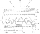
Fig. 1 and Fig. 2 show plan view and cross-sectional view strength according to the reflective liquid-crystal display 10 of first embodiment of the invention respectively at the part corresponding with pixel.
See figures.1.and.2, reflective liquid-crystal display 10 consists essentially of: lower glass substrate 11; Top glass substrate 14, its glass substrate 11 that faces down; And liquid crystal layer 13, it has negative dielectric anisotropic, and is arranged between substrate 11 and 14, and lower glass substrate 11 the gate 11B and the data electrode 11C that are provided with TFT (thin film transistor (TFT)) 11A thereon and cooperate with TFT 11A.For glass substrate 11, can utilize the conventional TFT substrate that in the transmissive liquid crystal display plate, uses.In this case, under the state that is electrically connected with TFT 11A, on glass substrate 11, be provided with pixel electrode 11D such as the such transparent conductor of ITO.
Be coated with reflecting electrode 12A on projection and the depression figure 12, wherein, the contact hole 11F of reflecting electrode 12A by forming in dielectric film 11E is electrically connected at the centre and the pixel electrode 11D of pixel region.
Projection and depression that reflecting electrode 12A formation and projection and depression figure 12 are corresponding, except its position corresponding with contact hole 11F, therefore, in pixel region, at the centre formation flat site corresponding with contact hole 11F.
On the other hand, on counter substrate 14, towards all even continuous formation opposite electrode 14A of a side of substrate 11, and on opposite electrode 14A, adopt the little resin or the dielectric material of specific inductive capacity of permittivity ratio liquid crystal layer 13 to form an arrangement control structure 12B at the position corresponding, be used to control the orientation of the liquid crystal molecule 13A in the liquid crystal layer 13 with contact hole 11F.
And, on substrate 11, form homeotropic alignment film 12C, with covering projection and depression figure 12 and reflecting electrode 12A, and on substrate 14, be provided with another homeotropic alignment film 12D, to cover opposite electrode 14A and arrangement control structure 12B.
It should be noted, alignment films 12C and 12D are used for the unactivated state in pixel, that is: do not apply under the state of driving electric field, in Fig. 2,, the liquid crystal molecule 13A in the liquid crystal layer 13 is arranged by on the direction vertical shown in the dotted line with substrate 11 or 14 cardinal principles to liquid crystal layer 13.On the other hand, because forming, the centre of the pixel in the LCD 10 of Fig. 1 and Fig. 2 arranges control structure 12B, thereby liquid crystal molecule tilts towards arranging control structure 12B, the result, in pixel region shown in Figure 3, form domain A-D, wherein, liquid crystal molecule is being tilted by the direction shown in the arrow.
And, form TAC (cellulose triacetate) film 15 in the outside of substrate 14, the about 100nm of its delay on thickness direction, and stacked above one another has phase compensation film 16 and the polarizer 17 that postpones about visible wavelength 1/4 on this TAC film 15.
In the reflective liquid-crystal display 10 of Fig. 1 and Fig. 2, oblique incidence is converted to linearly polarized photon to the surround lighting of polarizer 17 by polarizer 17, and incides liquid crystal layer 13 after being converted to circularly polarized light by 1/4 wave film 16.
Unactivated state in LCD 10, that is: do not apply under the state of voltage to the two ends of reflecting electrode 12A and opposite electrode 14A, it should be noted, as shown in Figure 2, liquid crystal molecule 13A is arranged in the liquid crystal layer 13 vertical with substrate 11 or 14 cardinal principles, and the circularly polarized light that incides liquid crystal layer 13 is reflected by reflecting electrode 12A.Therefore, reflected light is oppositely in turn by way of liquid crystal layer 13, TAC film 15 and 1/4 wave film 16, and is converted into linearly polarized photon, and this linear polarization polarization surface is revolved with respect to initial plane of polarization and turn 90 degrees.Therefore, linearly polarized photon is cut off by polarizer 17.
On the other hand, apply under the situation of driving voltage at two ends to reflecting electrode 12A and opposite electrode 14A, liquid crystal molecule 13A in the liquid crystal layer 13 is aligned to parallel substantially with liquid crystal layer 13 or tilts, and incides the circularly polarized light of liquid crystal layer 13 because the delay of liquid crystal layer 13 is converted to linearly polarized photon by 1/4 wave film 16 and TAC film 15.Then, so the linearly polarized photon that forms is reflected by reflecting electrode 12A, and in the opposite direction in turn by way of 1/4 wave film 16 and TAC film 15.Therefore, the linearly polarized photon that is reflected is converted into a kind of linearly polarized photon, and this linear polarization polarization surface is with the linear polarization polarization surface from the incident light conversion is identical at polarizer 17 places, and the linearly polarized photon that so obtains is by polarizer 17 outgoing.
In the reflective liquid-crystal display 10 of this formation, it should be noted, owing in reflecting electrode 12A, form contact hole 11F, make and do not form projection and depression figure 12 at the position corresponding with contact hole 11F, therefore, oblique incidence does not reflect back into the observer in the reflecting electrode 12A part that forms contact hole to the surround lighting of substrate 14.For this reason, in the reflective liquid-crystal display 10 of the formation with Fig. 1 and Fig. 2, can the problem that reflectivity descends take place in the centre of pixel inevitably.
And, adopt transparent resin to form even arrange control structure 12B, be used for optical loss is reduced to minimum, yet can not avoid by arranging the optical loss that control structure 12B is caused.
Therefore, in all structures as shown in Figure 4, that is: arrangement control structure 12B is formed on the centre of pixel region, and contact hole 11F is formed near the TFT 11C, and TFT 11C is arranged in this structure in peripheral position of pixel region, inevitably, when on the direction vertical, observing, in pixel region, form the low a plurality of zones of reflectivity with substrate 14.In this structure, the brightness severe exacerbation that image shows.
On the other hand, for the LCD 10 of Fig. 1 and Fig. 2, when on the direction vertical, observing, arrange control structure 12B and overlap, and reflectivity decline is suppressed to minimum with contact hole 11F with substrate 14.
And, from the cross-sectional view strength of Fig. 2 as can be seen, with form depression in protrusion type is arranged the zone of the corresponding contact hole 11F of control structure 12B, therefore, this depression has respectively lateral dimension and corresponding lateral dimension and the width of width with arrangement control structure 12B.As a result, arrange and also can keep identical substantially element thickness (cellthickness) in the zone of control structure 12B at this protrusion type that is formed with.
Below, will the manufacturing process of the reflective liquid-crystal display 10 of Fig. 1 and Fig. 2 be described.
In the present embodiment, the substrate of producing for transmissive type liquid crystal display is used as TFT substrate 11, and therefore, TFT substrate 11 is provided with thereon: TFT 11A, gate 11B, data electrode 11C, and transparent pixels electrode 11D.Then, by adopting the positive etchant resist of the about 1.2 μ m of whirl coating applied thickness,, thereby make TFT substrate 11 form resist layer so that this positive etchant resist covers TFT 11A, gate 11B, data electrode 11C and transparent pixels electrode 11D.
So the resist layer that forms has flat surfaces, after the prebake of carrying out 90 ℃, 30 minutes is handled, except the centre of pixel region, (will form contact hole), carry out ultraviolet treatment with irradiation, be used for by using mask to form projection and depression figure 12 in this centre.
Develop by resist layer, and formation projection and depression figure 12 are handled in the final oven dry of carrying out 200 ℃, 60 minutes that continues exposure like this.
Then, handle, make the projection and depression figure 12 coated aluminium (Al) films of formation like this, and, form the reflecting electrode 12A of pixel region by adopting photoetching process that the Al film of formation like this is carried out composition by carrying out evaporation deposition.
Below, will the formation of arranging control structure 12B be described.
At first, adopt whirl coating specific inductive capacity be 3.2, the just photosensitive transparent resin layer of the about 1.2 μ m of thickness is coated on the substrate 14, with coated electrode 14A.
Then, the resin bed of formation like this is carried out 90 ℃, 30 minutes prebake processing, use the ultraviolet exposure of mask to handle subsequently.And, handle by carrying out development treatment, post-exposure processing, 130 ℃, 2 minutes the first oven dry processing and 220 ℃, 6 minutes final oven dry in turn, form above-mentioned arrangement control structure 12B in the centre of pixel region.
And, homeotropic alignment film 12C that respectively comprises side chain diamine (side chain diamine) and 12D are coated in respectively on the surface of TFT substrate 11 and counter substrate 13, so that homeotropic alignment film 12C covers projection and depression figure 12 and reflecting electrode 12A, and make homeotropic alignment film 12D coated electrode 14A and arrange control structure 12B.
Then, the substrate 11 and 14 that makes preparation like this is by being that the pad (spacer) of 3 μ m piles up mutually between the diameter between the two, and a kind of liquid crystal, that is: having negative dielectric anisotropic (Δ ε=-3.5) and the refractive indices n between extraordinary ray and ordinary ray is that 0.067 liquid crystal is infused in the gap that forms between substrate 11 and 14.Therefore, can form the liquid crystal board of vertical alignment.
And, pile up TAC film 15,1/4 wave film 16 and polarizer 17 in turn by outside surface at substrate 14, the manufacturing process of reflective liquid-crystal display 10 is finished.
Fig. 5 is at a kind of situation, that is: the ratio of the homeotropic alignment component among homeotropic alignment film 12C and the 12D (side chain diamine) is set at 5%, 10% and 25% this situation with respect to whole amine component, the figure of the state of the black display mode in the LCD 10 of present embodiment is shown.
With reference to Fig. 5, as can be seen, under the ratio of the homeotropic alignment component in the homeotropic alignment film being set at 5% or 10% situation, producing light leak on a large scale, and be accompanied by this light leak, produce the problem that contrast rating descends.
On the other hand, the ratio of the homeotropic alignment component in alignment films 12C and 12D is that as can be seen, light leak seldom under 25% the situation.Therefore, can conclude from the result of Fig. 5, the ratio of the homeotropic alignment component among homeotropic alignment film 12C and the 12D should preferably be set to 25% or more than.
Generally, how little no matter the pitch angle has when liquid crystal molecules tilt, all can produce light leak.Yet, can think, when the pitch angle of liquid crystal molecule surpasses a certain threshold value, will the identification of people to this light leak situation appear.
For the transmissive type liquid crystal display that does not form projection or depression from the teeth outwards, when the ratio of the homeotropic alignment component in the molecular orientation film is 5%, can obtain enough contrast ratings.On the other hand, the result of Fig. 5 shows, if the ratio of the homeotropic alignment component in the alignment films be not set to 25% or more than, then can not in reflective liquid-crystal display, obtain enough contrast ratings.
With compare according to the result of first comparative experiments with the reflective liquid-crystal display of second comparative experiments (first comparative example and second comparative example), the reflectivity (brightness) and the contrast rating that obtain at white display mode in 1 pair of reflective liquid-crystal display of observing on the direction vertical with liquid crystal board 10 of following table are described, wherein, the measurement of table 1 is undertaken by using integration type sphere light source.On the other hand, in first comparative experiments, reflective liquid-crystal display uses inclined slot to replace in opposite electrode 14A and arranges control structure 12B, and in second comparative experiments, reflective liquid-crystal display uses on substrate 14 with arranging control structure 12B and similarly arranges control structure, but highly is 2.0 μ m.
Table 1
With reference to table 1, as can be seen, although in the present embodiment, homeotropic alignment component (side chain diamine) changes in 5 ~ 50% scope with respect to the ratio of total diamine component, yet the brightness that the reflective liquid-crystal display 10 of present embodiment obtains is higher than in first comparative experiments and second comparative experiments LCD of any one.And, as can be seen, by the ratio of homeotropic alignment component is set at 25% or more than, can obtain 23.0 or above contrast rating.
Consider the following fact, that is: TN mode reflection formula LCD can maximum provide only about 13% brightness and this fact of contrast rating of 18, will be appreciated that, compare with this TN mode reflection formula LCD, it is much superior that the reflective liquid-crystal display 10 available performances of present embodiment are wanted.
In table 1, be noted that with the reflective liquid-crystal display 10 of present embodiment and compare that under the reflective liquid-crystal display situation of first comparative experiments, the brightness of white display mode reduces about 30%.Can think that this result is produced by following effect, that is: near the liquid crystal molecule the slit in being formed at opposite electrode can not produce switching.
In second comparative experiments, it is also noted that the brightness that the brightness ratio present embodiment that is obtained is obtained is little by about 8%.Can think that this is because due to the delay minimizing of the liquid crystal layer that is positioned at the position on the arrangement architecture.It should be noted that the height of the arrangement architecture in second comparative experiments is greater than the arrangement architecture that uses in the present embodiment.
In the reflective liquid-crystal display 10 of present embodiment, also can form and arrange control structure 12B, in this case, this arrangement control structure 12B can use the big material of specific inductive capacity of permittivity ratio liquid crystal layer 13, make as shown in Figure 6, make this arrangement control structure 12B can be filled in the depression that TFT substrate 11 one sides corresponding with conductive plug 11F form.According to this formation, can realize that also liquid crystal molecule is towards the centroclinal molecules align of pixel region.
[second embodiment]
Below, will the reflective liquid-crystal display 20 according to second embodiment of the invention be described.
Fig. 7 shows the formation of reflective liquid-crystal display 20, and wherein, those parts corresponding with above-mentioned part are represented by identical reference numerals, thereby will be omitted its explanation.
With reference to Fig. 7, the formation of the formation of reflective liquid-crystal display 20 and the reflective liquid-crystal display of above explanation 10 is more or less similar, has only eliminated arrangement control structure 12B from substrate 11 or 14.
Be formed with the polymer chain 13B that has orientation in liquid crystal layer 13 in the LCD 20 of present embodiment, wherein, this polymer chain 13B is used to make liquid crystal molecule 13A to tilt towards the centre of pixel region.In Fig. 7, it should be noted that Ref. No. 13B only schematically shows polymer chain, and be not used in the practical structures of expression polymer chain, also be not used in each polymer chain of expression.
In more detail, as shown in Figure 8, be formed with the projection and the depression figure 12 that adopt the elongation graphic form on the TFT substrate 11 in the present embodiment, so that each projection figure extends on substrate vertical or horizontal.And, comprise the homeotropic alignment film that ratio is 25% homeotropic alignment component by use, form alignment films 12C and 12D.
With reference to Fig. 8, projection in the projection and the figure 12 that caves in and depression all are formed in each domain zone A-D that is schematically shown among Fig. 3, and wherein, each projection or depression are all extended on vertical or horizontal along the edge, neighboring of regional A-D.
And making substrate 11 and substrate 12 is that the pad of 3 μ m piles up mutually by diameter, and when ultraviolet ray is shone liquid crystal a kind of and that be used to form the mixed with resin of polymer chain is infused in the gap that forms between substrate 11 and 14.It is 0.3% resin that this liquid crystal can comprise part by weight.Use this liquid crystal, can form liquid crystal layer 13.In the present embodiment, use a kind of resin, when carrying out ultraviolet ray irradiation (I-line) with the intensity of 2000mJ/cm2, this resin produces photopolymerization.
In the reflective liquid-crystal display that so forms, with what note be, as shown in Figure 8, by forming on TFT substrate 11 laterally or the projection and the depression of longitudinal tensile strain, can make by projection in projection and the depression figure 12 and the catoptrical intensity that is recessed to form increases on the vertical and horizontal of substrate.On the other hand, in the projection and depression figure 12 of Fig. 1, as shown in Figure 9, this directive property can not appear in reflected light.
Therefore, in the present embodiment, LCD to acquisition like this applies the 4V driving voltage, and in this state, apply the ultraviolet ray irradiation to substrate 14, so that by the catoptrical intensity of projection and the reflection of depression figure 12 in liquid crystal layer 13, on the vertical and horizontal be 2000mJ/cm2 or more than.Owing to the catoptrical effect on the vertical and horizontal that form from the ultraviolet ray irradiation, thereby can in liquid crystal layer 13, form polymer chain 13B, this polymer chain 13B extends on the vertical and horizontal of substrate, and, because homeotropic alignment film 12C and 12D and so effect of the polymer chain 13B of formation, thereby can the liquid crystal molecule 13A in the liquid crystal layer 13 be arranged as shown in Figure 2.
The same with the situation of the reflective liquid-crystal display 10 of embodiment formerly, the meter of the brightness and contrast's coefficient that carries out on the reflective liquid-crystal display that so forms reveals similar result.
According to present embodiment, control with the shape of depression figure 12 by projection, and, can on any direction of light intensity, make the compound polymerization of photopolymerization for maximum by the compound of photopolymerization is included in the liquid crystal layer 13 to the uv reflectance irradiation.
[the 3rd embodiment]
Figure 10 shows the formation according to the reflective liquid-crystal display 30 of third embodiment of the invention, and wherein, those parts corresponding with above-mentioned part are represented by identical reference numerals, thereby will be omitted its explanation.
With reference to Figure 10, LCD has a kind of formation that the characteristics of first embodiment and second embodiment are mixed, wherein, as shown in Figure 8, glass substrate 14 is provided with thereon arranges control structure 12B, and the projection in the figure 12 has elongate form in projection and depression, the extension on substrate vertical or horizontal of this projection.And liquid crystal layer 13 comprises photopolymerization chain 13B within it.
In the LCD 30 of Figure 10, it should be noted, the absorption axes of polarizer 17 be set at substrate vertically on, and the direction of the retardation axis of 1/4 wave film 16 is configured to form miter angle with the absorption axes of polarizer 17.
Following table 2 is the brightness and contrast's coefficient that obtains at the reflective liquid-crystal display 30 that so obtains in white display mode and (the 3rd comparing embodiment: the 3rd comparative example) brightness and contrast's coefficient of Huo Deing is contrasted at a kind of similar reflective liquid-crystal display, in the latter, the direction of the absorption axes of polarizer 17 and substrate vertically between have 45 degree to depart from.
Table 2
| VA component % | Brightness % | Contrast | |
| The |
25 | 13 | 24.8 |
| The 3rd comparative example | 25 | 13 | 23.0 |
With reference to table 2, with what note be, between present embodiment and comparative experiments, aspect brightness, there is not substantial variation, what also will note simultaneously is that in the LCD of present embodiment, contrast rating improves.
Can think, this raising is that the improvement owing to black display mode realizes, the improvement of black display mode then is owing in a direction: promptly: the reflection strength of projection and depression figure 12 is set the absorption axes of polarizer 17 on for the direction of maximum and is realized.
[the 4th embodiment]
Figure 11 shows the formation according to the reflective liquid-crystal display 40 of fourth embodiment of the invention, and Figure 12 shows the ray propagates in the reflective liquid-crystal display 40 of Figure 11.In Figure 12, it should be noted to have only those parts relevant just to be represented, and omit expression other parts with the optical path length of light.
With reference to Figure 11, the LCD 40 of present embodiment generally comprises: lower glass substrate 41; Top glass substrate 44, its glass substrate 41 that faces down; And liquid crystal layer 43, it has negative dielectric anisotropic, and is arranged between top glass substrate 44 and the lower glass substrate 41, wherein, lower glass substrate 44 is provided with element thereon: TFT (not shown) for example, the gate 41C that cooperates with TFT, and data electrode (not shown).The standard TFT substrate that designs for transmissive type liquid crystal display can be used as glass substrate 44.In this case, under the state that is electrically connected with TFT, on glass substrate 41, be formed with the pixel electrode 41D of the transparent conductor as ITO.
It should be noted that TFT, gate 41C and data electrode by etchant resist is carried out composition and processing, can form projection and depression figure 42 all by covering such as the such dielectric film of resin on dielectric film 41E.
Projection and depression figure 42 are covered by aluminium reflecting electrode 42A such as (Al), and the contact hole 41F of this reflecting electrode by forming in dielectric film 41E, preferably are connected with pixel electrode 41D in the centre of pixel region.
On top glass substrate 44, at all even opposite electrode 44A that is formed with continuously in surface towards the substrate 44 of substrate 41.
And, on substrate 41, form homeotropic alignment film 42C, so that cover projection and depression figure 42 and reflecting electrode 42A, and on substrate 44, be formed with another homeotropic alignment film 42D, so that cover opposite electrode 44A.
In unactivated state, that is: do not apply under the state of driving electric field to liquid crystal layer 43, alignment films 42C is used for making Liquid Crystal Molecules Alignment on the direction vertical with substrate 41 or 44 cardinal principles with 42D, and as shown in figure 12, owing to have projection and depression figure 42, thereby produce with the liquid crystal molecule that depression figure 42 contacts with projection.
And, form preferably by the film formed phase compensation film 45 of TAC in the outside of substrate 44, and 1/4 wave film 46 and polarizer 47 further are layered on the phase compensation film 45 in turn.
In the reflective liquid-crystal display 40 of present embodiment, it should be noted that the liquid crystal molecule 43A that constitutes liquid crystal layer 43 is not limited to have the liquid crystal molecule of negative dielectric anisotropic, and also can be the liquid crystal molecule with positive dielectric anisotropy.Even in this case, due to the fact that, that is: under the unactivated state of LCD, liquid crystal molecule 43A arranges this fact on the direction vertical with the plane cardinal principle of substrate 41 or 44, and LCD 40 also is a reflective liquid-crystal display.
In the above-described embodiments in Shuo Ming the VA mode reflection formula LCD 10 ~ 30, it should be noted, in view of the surround lighting oblique illumination arrives liquid crystal layer 13 these facts, and in view of liquid crystal molecule 13A by projection and depression figure 42 this facts that tilt, under the unactivated state of LCD, liquid crystal layer 13 also demonstrates delay.Therefore, only under the unactivated state of above-mentioned VA mode LCD, the delay of liquid crystal layer 13 just can obtain the desirable black display of expectation after being compensated by phase compensation film etc. under the unactivated state of above-mentioned VA mode LCD.
For VA pattern transmissive type liquid crystal display, in No. 1462978 BrP, perhaps in the 10-153802 Japanese laid-open patent is open, a kind of technology has been proposed, be used to use phase compensation film to compensate the delay of homeotropic alignment liquid crystal layer.
In these are proposed, the delay of the phase compensation film that is given as df{ (nx+ny)/2-nz} set for the delay of the liquid crystal layer that is defined as dlc Δ n equate substantially, wherein, df represents the thickness of phase compensation film, nx, ny and nz are illustrated respectively in the refractive index of the phase retardation film on x direction, y direction and the z direction, dlc represents the thickness of liquid crystal layer, and Δ n is illustrated in extraordinary ray in the liquid crystal layer and the refringence between the ordinary ray.
In this technology of VA pattern transmissive type liquid crystal display, phase compensation film only is used for stopping oblique incidence light at black display mode, and be used to improve the visual angle, and when being applied to VA mode reflection formula LCD, but can not obtain the expectation compensation of black display mode.
It should be noted that the VA mode reflection formula LCD that has projection and depression on reflecting surface is designed to obtain surround lighting as much as possible, and be used for the reflection of ambient light of being obtained to the observer.
With reference to Figure 12, with refraction angle θ 2 refractions, this refraction angle θ 2 is recently determined by the refractive index between air and the phase compensation film, and this surround lighting shines in the liquid crystal layer 43 with incident angle θ 3 with the surround lighting of incident angle θ 1 oblique incidence.
At the interface, the ordered state of liquid crystal molecule 43A is controlled on the direction vertical with the plane cardinal principle of substrate 44 by unshowned homeotropic alignment film 42D among Figure 12 between liquid crystal layer 43 and substrate 44.For this reason, the near interface of incident light between liquid crystal layer 43 and substrate 44 shines liquid crystal molecule 43A with angle θ 3.At this, it should be noted that the refractive index of liquid crystal layer is about 1.5, and approximate the refractive index of phase compensation film 45.For this reason, can think that incident angle θ 3 is approximately equal to incident angle θ 2.
On the other hand, in this VA mode reflection formula LCD, described as reference the foregoing description, be necessary the surround lighting of emission oblique incidence on the direction vertical with substrate 44, and for this purpose, on TFT substrate 41, form projection and depression figure 42.
In Figure 12, this projection and depression figure 42 are similar to the taper of the transversal section with isosceles triangle.Therefore, on projection and depression figure 42, because homeotropic alignment film 42C has the function that covers projection and depression figure 42, liquid crystal molecule 43A is aligned to vertical with hypotenuse, and wherein the plane of this hypotenuse and substrate 41 forms angle ξ.
Therefore, in liquid crystal layer 43, liquid crystal molecule 43A increases progressively the pitch angle on the thickness direction of liquid crystal layer 43, from be incremented between liquid crystal layer 43 and projection and depression figure 42 ξ value at the interface at the interface 0 value between liquid crystal layer 43 and the substrate 44.Therefore, the near interface between liquid crystal layer 43 and substrate 41, the incident angle of light that shines liquid crystal molecule 43A is because projection and the depression inclination that produces in liquid crystal molecule 43A of figure 42 and reduce angle ξ from above-mentioned angle θ 3.
Therefore, the incident light that enters liquid crystal layer 43 from phase compensation film 45 shines projection and depression figure 42 with incident angle ξ, and also reflects with reflection angle ξ.As a result, reflected light shines the liquid crystal molecule 43A of homeotropic alignment on projection and depression figure 42 once more with incident angle ξ.
At the interface, the orientation of liquid crystal molecule is controlled so as to vertical with the plane of substrate 41 between liquid crystal layer 43 and substrate 41.Therefore, liquid crystal molecule 43A progressively 44 change orientations on the thickness direction of liquid crystal layer 43 from substrate 41 to substrate.Be associated therewith, the catoptrical incident angle that incides liquid crystal molecule 43A is successively decreased gradually, and in the vanishing at the interface to substrate 44.
In the optical system of Figure 12, the optical path length in the phase compensation film 45 in the first half (being defined as arriving the light path of the projection and the incident light of depression figure 42) of light path is given as dv/cos θ 2, wherein, and in view of relational expression
 , this optical path length is approximately equal to dv/cos2 ξ.And the optical path length of the incident light in the
 liquid crystal layer 13 is given as dlc/cos2 ξ.On the other hand, in liquid crystal layer, be given as dlc by the projection and the catoptrical optical path length of figure 42 vertical reflections that cave in, and in phase compensation film 45, be given as dv to the principal plane of substrate 41.
Therefore, the VA mode reflection formula LCD 40 that inclination enters for surround lighting, with what note be, because the different light path lengths between input path and emitting light path, even if under the unactivated state of LCD, also delay be can produce, and incident angle θ 1 and angle ξ that size depends on projection and depression figure 42 postponed.
In an example, that is: the thickness d lc of liquid crystal layer 43 is 3 μ m, refractive indices n is 0.067, and average slope angle<ξ that projection and depression figure 42 provide〉be in the example of 13 degree, shown in the example A of following table 3, in unactivated state, that is: do not apply under the state of driving voltage to LCD, the delay of liquid crystal layer 43 is calculated as 33nm, but condition is that the incident angle θ 1 of incident light is set to 25 degree.
Table 3
| Reverberator | <ξ> | The delay of liquid crystal | Phase differential | 1. | Compensation |
| A | 13.06 | 33.25 | 15.26 | 45.9% | |
| B | 8.98 | 15.98 | 9.05 | 56.6% | |
| C | 7.67 | 13.01 | 7.92 | 60.9% | |
| D | 7.48 | 11.87 | 7.53 | 63.4% |
Table 3 (continuing)
| Reverberator | Phase differential 2. | Compensation |
| A | 29.65 | 89.2% |
| B | 16.15 | 101.1% |
| C | 13.71 | 105.4% |
| D | 12.85 | 108.3% |
Table 3 (continuing)
| Reverberator | Phase differential 3. | Compensation |
| A | 36.32 | 109.2% |
| B | 19.04 | 119.1% |
| C | 15.94 | 122.5% |
| D | 14.82 | 124.9% |
Table 3 (continuing)
| Reverberator | Phase differential 4. | Compensation |
| A | 51.34 | 154.4% |
| B | 25.96 | 162.5% |
| C | 21.42 | 164.6% |
| D | 19.76 | 166.5% |
In table 3, it should be noted, except example A, example B, example C and example D have also been enumerated, wherein, example B represents average slope angle<ξ〉be set to 9 the degree examples, example C represents average slope angle<ξ〉be set to 7.7 the degree examples, example D represents average slope angle<ξ〉be set to 7.5 the degree examples.
In order to compensate this delay that liquid crystal layer 43 medium dips produce, can use a kind of film that on the direction vertical, has negative dielectric anisotropic with substrate.
Therefore, table 1 also show in an inclined direction length of delay and the compensation efficient of these examples, in these examples, the refringence of phase compensation film 45 (nx+ny)/2-nz} is: 0.0006 (phase differential is 1.), (0.0013 phase differential 2.), (0.0017 phase differential 3.), and 0.0024 (phase differential 4.).
Below, will be to describing by the inclination delay compensation of using this phase compensation film 45 to obtain with negative dielectric anisotropic.
Figure 13 A shows the indicatrix of the phase compensation film 45 that has negative dielectric anisotropic on the substrate vertical direction, and Figure 13 B shows the indicatrix of the liquid crystal layer 43 with positive dielectric anisotropy.And Figure 14 A shows the transversal section of the indicatrix of Figure 13 A that is got in the Y-Z plane, and Figure 14 B shows the transversal section of the indicatrix of Figure 13 B that is got in the Y-Z plane.In the following discussion, suppose in any one of phase compensation film 45 and liquid crystal layer 43 all do not have intra-face anisotropy (nx=ny).
With reference to Figure 13 A and 13B and with reference to Figure 14 A and 14B, with what note be, the refractive index that incides the ordinary ray of light of X-Y plane and extraordinary ray with incident angle θ is in phase compensation film 45 situations, corresponding with long axis of ellipse and minor axis, and under liquid crystal layer 43 situations, corresponding with the minor axis and the main shaft of ellipse, this ellipse is to form on the transversal section of the indicatrix of being got section by a plane.
With reference to Figure 14 A and Figure 14 B, for a kind of situation, that is: incident light becomes angle θ to shine this situation with the normal direction (Z direction) of substrate, according to following equation, obtains the apparent refractive index n y ' and the nz ' of expression refractive index on Y direction and Z direction respectively.
In the formula:
The length of delay of the liquid crystal layer of expression and phase compensation film and compensation efficiency value all according to apparent refractive index n x ', ny ' and nz ' and incident angle θ calculating, therefore, comprise the effect of incident light inclination light path in the last table 3.
Refer again to table 3, as can be seen, 1. and 4. phase compensation film can not provide abundant compensation, and 2. and 3. phase compensation film can provide nearly 100% compensation.
It should be noted that this delay compensation changes along with the delay dlc Δ n of liquid crystal layer, therefore, when the delay of liquid crystal layer changed, delay compensation also must change.
Generally, length of delay is represented by the value on the direction parallel or vertical with substrate.Therefore, preferably, the delay of phase compensation film is also used with the value on the parallel or vertical direction of substrate and is represented, and need not represent with the tilting value of substrate.
Therefore, be the situation of the reverberator A of 13 degree at average slope angle ξ, the preferred length of delay of above-mentioned acquisition is represented as:
0.5≦[df·{(nx+ny)/2-nz}]/(dlc·Δn)≦0.7
In this scope,, yet also can obtain remarkable result at black display mode although can exist delay compensation and optimum value to depart from about 10% this situation.
On the other hand, be that the delay of liquid crystal layer 43 under unactivated state is in 11 ~ 16nm scope under the situation of 7 ~ 9 reverberator B ~ D that spend using average slope angle ξ.In this case, 2. phase compensation film provides optimum.In this case, the preferred delay scope of this phase compensation film is confirmed as:
0.4≦[df·{(nx+ny)/2-nz}]/(dlc·Δn)≦0.6
The allowance of allowing that comprises optimum value.
Sum up The above results and can conclude that the preferred delay scope of the phase compensation film 45 of reflective liquid-crystal display 40 is defined in the following scope, that is:
0.4≦[df·{(nx+ny)/2-nz}]/(dlc·Δn)≦0.7
When pitch angle ξ reduces to about 7 degree when following, the incident angle θ 1 that is used to obtain surround lighting is too little, and is difficult to obtain surround lighting.
In the formation of Figure 11, particularly advantageous being to use has the TAC film that has about 50nm delay on about 10nm delay and the normal direction on the direction in the face of phase compensation film 45.Use this film, can low-costly realize desirable substantially black mode compensation.
It should be noted that polarizer 47 generally has the TAC damp-proof membrane, but this TAC film is arranged between 1/4 wave film 46 and the polarizer 47.Therefore, the compensation effect that adopts this damp-proof membrane to obtain can't be comparable with the compensation effect that uses phase compensation film 45 to obtain.This names a person for a particular job in following explanation.
In the LCD 40 of Figure 11,1/4 wave film 45 is arranged between phase compensation film 45 and the polarizer 47, and wherein, this 1/4 wave film is compared with liquid crystal layer 43, demonstrates less wavelength dispersion.
Therefore, by the less phase compensation film of this wavelength dispersion is arranged between polarizer 47 and the liquid crystal layer 43, and by realizing 90 degree rotations of plane of polarization, can realize with wavelength dispersion being the good black mode demonstration of feature less, and therefore can realize the small leakage of visible light.
By doing like this, the outside that 1/4 wave film 46 (i.e. second phase compensation film) is arranged on phase compensation film 45 (i.e. first phase compensation film) is not preferred.It should be noted, the indicatrix of phase compensation film 45 has the orientation dependence, and this formation that 1/4 wave film 46 is arranged between phase compensation film 45 and the liquid crystal layer 43 will produce a kind of situation, that is: the linearly polarized photon by way of polarizer is compensated.In this case, can exist a problem to be, use particular azimuth can obtain gratifying compensation, and use other position angles can not obtain this gratifying compensation.Therefore, total compensation effect descends.
If 1/4 wave film 46 is formed on the outside of phase compensation film 45, then 45 pairs of light phases by way of the circularly polarized light of 1/4 wave film 46 of phase compensation film compensate, and the dependent effect in orientation is eliminated.It should be noted that circularly polarized light is equivalent on all azimuth directions, therefore,, can both realize light compensation at all azimuth directions in this case even when on the indicatrix of phase compensation film 45, having the orientation dependence.
Simultaneously, has retardation axis in the face such as TAC film 45 such phase compensation films.Therefore, produce a problem and be, when this TAC film 45 and 1/4 wave film 46 were stacked, the delay of 1/4 wave film 46 was affected.If 1/4 wave film 46 and phase compensation film 45 be at a kind of state, for example, each retardation axis overlaps stacked under this state, and then this stepped construction length of delay on the direction in face is the length of delay sum of phase compensation film 45 and 1/4 wave film 46.Retardation axis intersects vertically if they are arranged to make separately, then postpones poor for the length of delay of phase compensation film 45 and 1/4 wave film 46.
Therefore, if the element of 1/2 wave film and the stacked formation of 1/4 wave film is used for 1/4 wave film 46, in order to wavelength dispersion is reduced to minimum, a problem then can occur is, if retardation axis departs from the interior retardation axis of face of 1/4 wave film 46 in the face of phase compensation film 45, then phase compensation film 45 is included in the stepped construction.Therefore, can there be the affected possibility of wavelength dispersion characteristic.
For fear of this problem, the interior retardation axis of face of the TAC film that forms phase compensation film 45 is overlapped with the interior retardation axis of the face of 1/2 wave film that constitutes stacked 1/4 wave film 46 or 1/4 wave film.In this case, except postponing increase or reducing, can not produce other influences.
Particularly, by adopting a kind of relation that phase compensation film 45 and 1/4 wave film 46 are set so that in the face separately retardation axis be parallel to each other and extend and make that to postpone sum in the face be almost 1/4 of visible wavelength, can realize the full remuneration of black display.By doing like this, can suppress the delay distortion of 1/4 wave film 46 that postpones to be produced in the face by 1/4 wave film 46.
Especially, if 1/4 wave film 46 is the elements in the above-mentioned stepped construction, then make any one the interior retardation axis of face of retardation axis and 1/4 wave film or 1/2 wave film in the face of phase compensation film 45 aim at just enough.And, postpone to adjust, equal 1/4 wavelength so that postpone sum in the face of 1/4 wave film and phase compensation film 45, perhaps equal 1/2 wavelength so that postpone sum in the face of 1/2 wave film and phase compensation film 45.In this case, postponing sum in the face of phase compensation film 45 and stacked 1/4 wave film 46 does not always equate with 1/4 of visible wavelength.Yet, when the delay of one of them phase compensation film in stacked 1/4 wave film 46 is adjusted, so that when postponing to equal 1/4 visible wavelength in the face of stacked 1/4 wave film, 46 integral body, can obtain similar effect.
Below, will the manufacturing process of the reflective liquid-crystal display 40 of Figure 11 be described.
In the present embodiment, adopt whirl coating that the etchant resist of the about 1 μ m of thickness is coated on the TFT substrate 41, and the prebake of carrying out 90 ℃, 30 minutes is handled.Afterwards, make the etchant resist of formation like this be exposed to the ultraviolet ray irradiation, use simultaneously and projection and depression figure corresponding mask.By etchant resist is developed, and the oven dry of carrying out subsequently 135 ℃, 40 minutes is handled and 200 ℃, 60 minutes final oven dry is handled, and can use the average slope angle<ξ of 7.7 degree〉form projection and depression figure 42.It should be noted,, can change this pitch angle arbitrarily by changing bake out temperature and drying time.
And, adopt the evaporation deposition method, can make thickness is that aluminium (Al) the film 42A of 200nm is deposited on the surface of the projection of formation like this and depression figure 42.
And, homeotropic alignment molecular orientation film 42C and 42D are coated on the TFT substrate 41 and counter substrate 44 of processing like this, and the substrate of so handling 41 and 44 are fitted together, and obtain hollow plate by the intervention pad that diameter is 3 μ m.
Then, a kind of liquid crystal, that is: having negative dielectric anisotropic (Δ ε=-3.5) and the refractive indices n between extraordinary ray and ordinary ray is that 0.067 liquid crystal is infused in the gap that forms between aforesaid substrate 41 and 42.Use this liquid crystal, can obtain liquid crystal board.
Then, postponing in the face to postpone two twin shaft TAC film-stack for 47nm on substrate 44 for 10nm and normal direction, as phase compensation film 45, so that retardation axis has 85 position angles of spending in the face, and postponing in the face to stack gradually for 1/2 wave film of 250nm, and the position angle of retardation axis is set at 140 respectively spends and 85 spend for postponing in 1/4 wave film of 135nm and the face.Therefore, form stacked 1/4 wave film 46.And, on 1/4 wave film 46, form polarizer 47, so that absorption axes is oriented on the azimuth direction of 75 degree.
In the VA mode reflection formula LCD 40 that so forms,, can suppress wavelength dispersion by using stacked 1/4 wave film as 1/4 wave film 46.And, retardation axis overlaps in the face with 1/2 wave film of stacked 1/4 wave film 46 of formation by the direction setting of retardation axis in the face of phase compensation film 45 is become, can make the interior retardation of face of the interior length of delay minimizing of the face phase compensation film 45 of 1/2 wave film, and 1/4 wave film, 46 integral body demonstrate length of delay in the face corresponding with 1/2 wavelength when green wavelength (540nm), wherein at this green wavelength, the sensitivity maximum of human eye.
On the other hand, phase compensation film 45 is a kind of films with negative dielectric anisotropic, is used in the delay that applies compensation liquid crystal layer under the state of electric field, wherein, postpone df{ (nx+ny)/2-nz} in the face of phase compensation film 45 at postponing dlc Δ n in the face of liquid crystal layer 43, satisfy following relational expression:
df·{(nx+ny)/2-nz}/(dlc·Δn)=0.47
Following table 4 shows at the each side in white display mode and the black display mode, the measurement result of the reflectivity of the reflective liquid-crystal display 40 that so obtains by applying predetermined drive voltages.The measurement of table 4 is undertaken by using spectrometer, and this spectrometer uses integration type sphere light source (the 4th embodiment).It should be noted that integration type sphere light source is a kind ofly to be used for radiative diffused light source on all angles and all azimuth directions, and the illumination that approaches such as the such surround lighting of room lighting or daylight can be provided.
Table 4

With reference to table 4, as can be seen, the reflective liquid-crystal display 40 of present embodiment can obtain 0.53 reflectivity when black display mode, and can obtain 12.64 reflectivity when white display mode.Use this reflective liquid-crystal display 40, can obtain 24.1 contrast rating.
In table 4, also enumerated the result of the 4th comparative experiments to the seven comparative experiments (the 4th comparative example to the seven comparative examples).
In the 4th comparative experiments, make the order of phase compensation film 45 and stacked 1/4 wave film 46 reverse, therefore, substrate 44 at first covers with 1/4 wave film of stacked 1/4 wave film 46,1/2 wave film with stacked 1/4 wave film 46 covers then, covers phase compensation film 45 at last on above-mentioned 1/2 wave film.Otherwise the formation of using among the formation of the LCD of the 4th comparative experiments and the 4th embodiment is identical.
On the other hand, in the 5th comparative experiments, use and the similar LCD of using in the 4th embodiment of LCD, the uniaxial film that 1/2 wave film that only constitutes the upper strata of stacked 1/4 wave film 46 is 270nm with the interior delay of a face substitutes.And, be arranged to 1/4 wave film in stacked 1/4 wave film 46 to make the grappling orientation (friction is directed) of retardation axis with the liquid crystal layer of 1/4 wave film consistent.Thus, compare, can make to postpone to reduce 20nm in the face with 1/4 wave film of the 4th embodiment.
On the other hand, in the 6th comparative experiments, can cancel the phase compensation film 45 of the LCD of the 4th embodiment.And postponing to be used for 1/2 wave film for the uniaxial film of 270nm in the face, this 1/2 wave film constitutes the part of stacked 1/4 wave film.
On the other hand, in the 7th comparative experiments, horizontal film is coated to substrate 41 and 44, and is that the pad of 3 μ m is assembled substrate 41 and 44 mutually by diameter.And a kind of liquid crystal, that is: a kind of to have positive dielectric anisotropy (Δ ε=6.0) and the refractive indices n between extraordinary ray and ordinary ray be that 0.067 liquid crystal is enclosed in the gap that forms between substrate 41 and 42.Therefore, the LCD of this comparative experiments is a TN mode reflection formula LCD.
Refer again to table 4, with what note be, any other LCD in these comparative experiments of the luminance factor of the LCD of present embodiment in black display mode is low, and the result uses the LCD of the 4th embodiment, can obtain high contrast ratio.
Figure 15 and Figure 16 are at the situation of using pointolite with the incident angle irradiating liquid crystal display 40 of 25 degree, show reflectivity and contrast rating according to the black display mode of the VA mode reflection formula LCD 40 of present embodiment (the 4th embodiment), wherein, Figure 15 shows reflectivity, and Figure 16 shows contrast rating.And Figure 15 shows the similar measurement result relevant with the device of the 6th comparative experiments with Figure 16.
With reference to Figure 15 and Figure 16, as can be seen,, compare with the LCD of comparative experiments at whole position angle, in the reflective liquid-crystal display 40 of present embodiment, the reflectivity of black display mode reduces, and can realize the raising of contrast rating.
Generally, have a kind of tendency to be, the reflectivity in the black display mode is in having the reflective liquid-crystal display of single polarizer, and is minimum on the azimuth direction corresponding with the absorption axes of polarizer, and maximum on the azimuth direction corresponding with the axis of homology.
In Figure 15 and Figure 16, can find out that also the reflectivity in the black display mode is obtained minimum value when corresponding with the absorption axes of polarizer 47 nearly 255 degree position angles, and obtains the maximum-contrast coefficient when this position angle.
Following table 5 shows with the LCD of the 6th comparative experiments and compares, the black display mode on the direction of the absorption axes of polarizer of the LCD 40 of the 4th embodiment and the reflectivity of white display mode, and the dependence in contrast rating and orientation.
Table 5

With reference to Fig. 5, as can be seen, when corresponding with the direction of the absorption axes of polarizer about 255 degree position angles, to compare with this comparative experiments, the reflectivity of black display mode reduces 18% in the present embodiment.And table 5 shows that when this position angle, contrast rating increases to 67.5% from 48.7%.
[the 5th embodiment]
Below, will the reflective-transmissive formula LCD according to fifth embodiment of the invention be described.
Figure 17 shows the general formation of conventional reflective-transmissive formula LCD.
With reference to Figure 17, reflective-transmissive formula LCD 50 consists essentially of: a pair of glass substrate 51 and 52, and liquid crystal layer 53, it is arranged between glass substrate 51 and 52, wherein, is formed uniformly transparency electrode 52A at the inside surface of glass substrate 52.On the other hand, at the inside surface formation planarization film 51A of glass substrate 51, and in this planarization film 51A, form opening 51a, as the optical transmission window.
Surface at planarization film 51A forms the reflecting electrode 51B with projection and depression, and corresponding to above-mentioned opening 51a, forms transparency electrode 51C on substrate 51.
And, form a circular polariscope 54 in the outside of substrate 51, and form another circular polariscope 55 in the outside of substrate 52.
Realize in the reflective-transmissive formula LCD 50 that light switches by the delay of liquid crystal layer 53 is modulated this, be necessary passing through that glass substrate 52 incides liquid crystal layer 53 and after by reflecting electrode 51B reflection, set for and enter liquid crystal layer 53 from substrate 51 by optical window 51a and equate in the liquid crystal layer 53 at optical path length by way of the light of liquid crystal layer 53 and glass substrate 52 outgoing afterwards from the optical path length of the light of liquid crystal layer 53 outgoing.That is to say, be necessary to form the planarization film 51A that thickness is liquid crystal layer 53 thickness 1/2.
Yet in view of the needs following steps, the manufacturing of this LCD is complicated, and these steps are used to make the common manufacturing step of LCD except comprising, also comprise: form thick planarization film 51A on substrate 51; On planarization film 51A, form reflecting electrode 51B; Form optical window 51a; And, on substrate 51, form transparency electrode 51C corresponding to optical window 51a.Therefore, conventional reflective-transmissive formula LCD 50 can run into the problem that cost increases.
And, in the reflective-transmissive formula LCD 50 of Figure 17, need be used to the corrosion that prevents that electrolytic effect from producing at the 51b of formation barrier metal film at the interface between aluminium (Al) reflecting electrode 51B and the ito transparent electrode 51C.
On the other hand, Figure 18 shows the formation according to the reflective-transmissive formula LCD 60 of fifth embodiment of the invention that is used to eliminate the problems referred to above.
With reference to Figure 18, LCD 60 consists essentially of: a pair of glass substrate 61 and 62, and polymer network liquid crystal layer 63, it is arranged between glass substrate 61 and 62, wherein, is formed uniformly transparency electrode 62A at the inside surface of glass substrate 62.
Form the reflecting electrode figure 61A with slot-shaped opening 61a at the inside surface of glass substrate 61, and liquid crystal layer 63 is in the unactivated state of LCD, that is: the state that does not apply driving voltage to liquid crystal layer 63 adopts the optical clear state down.On the other hand, in state of activation, that is: apply under the state of driving electric field to liquid crystal layer 63, liquid crystal layer 63 adopts scattering state.By using the polymer network liquid crystal that for example in the 5-27228 Japanese laid-open patent is open, discloses, can realize this liquid crystal layer 63.
And, be provided with circular polariscope 64 in the outside of glass substrate 61, and be provided with linear polarizer 65 in the outside of glass substrate 62.
Figure 19 A and Figure 19 B are used for respectively figure that the reflective-transmissive formula LCD of Figure 18 is described in the operation of black display mode and white display mode.
With reference to Figure 19 A, this figure left side shows the reflective-mode operation, and the right side shows the transmission mode operation, wherein, with what note be, incident light from the liquid crystal board front side is converted to linearly polarized photon by linear polarizer 65 in the reflective-mode operation, and further is converted to circularly polarized light by the liquid crystal layer 63 that is in non-scattering state.It should be noted that the delay of liquid crystal layer 63 is about 1/4 of lambda1-wavelength, and have retardation axis that this retardation axis forms miter angle with respect to the absorption axes of polarizer 65.At this, it should be noted that the delay of the liquid crystal layer 63 under non-scattering state never is limited to 1/4 of lambda1-wavelength λ or visible wavelength, but can have following value, that is: (0.5n+1/4) λ; N=0,1,2...n, wherein, n is a natural number.
Then, the incident light that so is converted to circularly polarized light is reflected under the circularly polarized light state by reflecting electrode 61A, and is converted into the linearly polarized photon with plane of polarization, and this plane of polarization intersects vertically with initial plane of polarization.Then, this have this linear polarization state and cut off by linear polarizer 65 from the reflected light of liquid crystal layer 63 outgoing, and obtain the black display of expectation.
In transmission mode operation, the incident light that incides substrate 61 from the dorsal part of liquid crystal board is converted into circularly polarized light by way of circular polariscope 64 time, and is imported into liquid crystal layer 63 by the optical window 61a among the reflecting electrode 61A.
Because liquid crystal layer 63 is in non-scattering state, thereby the circularly polarized light of incident is converted into the linearly polarized photon with the plane of polarization that intersects with the absorption axes of linear polarizer 65 by way of liquid crystal layer 63 time, the situation of the circularly polarized light of this and above-mentioned reflection is similar, and, also cut off by linear polarizer 65 by way of the transmitted light of liquid crystal layer 63.
On the other hand, in the white display mode of Figure 19 B, liquid crystal layer 63 is in scattering state, and is scattered by way of linear polarizer 65 and the linearly polarized photon that incides liquid crystal layer 63, and this scattered light is reflected by reflecting electrode 61A.It should be noted, this scattered light carries out further scattering during oppositely by way of liquid crystal layer 63 after reflection, the result, linear polarizer 65 receives a kind of light, this light also comprises the various polarization component of various plane of polarizations except comprising the polarization component with plane of polarization parallel with the absorption axes of linear polarizer 65.
Therefore, by way of polarizer 65, and the white that obtains expectation shows this polarization component with the plane of polarization that intersects with absorption axes with the form of linearly polarized photon.
Identical explanation also is applicable to the situation of transmitted light.Therefore, the incident light that incides substrate 61 by circular polariscope is scattered at liquid crystal layer 63, and those polarization component that form because of scattering and have the plane of polarization that intersects with the absorption axes of polarizer 65 are by way of polarizer 65.
In the reflective-transmissive formula LCD of this formation, the electrode 51B that need not to form thick planarization film 51A or have diffusing structure also need not to form the transparency electrode 51C corresponding with optical window 51a.It is just enough only to need to form reflecting electrode 61A, and the inside surface that this reflecting electrode 61A is patterned at substrate 61 forms the slit.And, it should be noted that reflecting electrode 61A can not contact with transparency electrode, therefore, need not to form barrier metal layer.
Therefore, the manufacturing process of the LCD of present embodiment is carried out easily, and manufacturing cost significantly reduces.
And, it should be noted that there is not the limited problem in visual angle in this LCD that liquid crystal layer state exchange between non-scattering state and the scattering state is used, and can obtain good viewing angle characteristic.
In the example of Figure 18, it should be noted that under non-scattering state, the length of delay of liquid crystal layer is 1/4 of a lambda1-wavelength.On the other hand, also can use the liquid crystal layer with few delay shown in Figure 20, wherein, it should be noted, Figure 20 shows the LCD 70 according to the modification of present embodiment.In Figure 20, those parts corresponding with above-mentioned part are represented by identical reference numerals, thereby will be omitted its explanation.
With reference to Figure 20, in reflective liquid-crystal display 70, use a kind of polymer dispersed liquid crystal layer 73 that postpones in few face that under non-scattering state, has, to replace liquid crystal layer 63.The long-pending Δ nd of the used liquid crystal of retardation ratio scattering layer is little in the face of liquid crystal layer 73, and wherein, Δ n represents birefraction, and d represents element thickness.Therefore, preferably postponing in the face to set in liquid crystal layer 73 and can ignore.Be associated therewith, replace linear polarizer with circular polariscope 66.
Figure 21 A and Figure 21 B show the operation of reflective-transmissive formula LCD 70 in black display mode and white display mode of Figure 20 respectively.
With reference to Figure 21 A, this figure left side shows the reflective-mode operation in the black display mode, and this figure right side shows the transmission mode operation.Therefore, in reflective-mode, be converted to circularly polarized light by circular polariscope 66 from the incident light of liquid crystal board front side, wherein, in view of the delay of liquid crystal layer 73 little of ignoring, so the circularly polarized light that forms under the circularly polarized light state by way of liquid crystal layer 73.This liquid crystal layer is in non-scattering state.
So the incident light by way of liquid crystal layer 73 is reflected under the circularly polarized light state by reflecting electrode 61A, and oppositely by way of liquid crystal layer 73, keeps the circularly polarized light state simultaneously.So the circularly polarized light by way of liquid crystal layer 73 oppositely enters circular polariscope 66, and is cut off.
On the other hand, in the transmission mode operation, the incident light that incides substrate 61 from dorsal part is converted to circularly polarized light by circular polariscope 64, and is introduced into liquid crystal layer 73 by the optical window 61a among the reflecting electrode 61A.
Because liquid crystal layer 73 is in non-scattering state, thereby the circularly polarized light of incident keeps the circular polarization state simultaneously by way of liquid crystal layer 73, and cut off by circular polariscope 66, and the circularly polarized light of this and above-mentioned reflection is similar.
In the white show state of Figure 19 B, liquid crystal layer 73 is in scattering state, and therefore, the circularly polarized light that incides liquid crystal layer 73 carries out scattering in liquid crystal layer 73.Then, the incident light of this scattering is reflected by reflecting electrode 61A, and carries out further scattering by liquid crystal layer 73 backpropagations the time.As a result, circular polariscope 66 receives in the front side and has the various polarization component of various plane of polarizations.
Therefore, this component with plane of polarization vertical with absorption axes is by way of polarizer 66, and the white that obtains to expect shows.
Same situation also is applicable to the situation of transmitted light, that is: the incident light that incides substrate 61 by circular polariscope 64 from dorsal part is scattered liquid crystal layer 73, and the polarization component that forms because of scattering and have the plane of polarization that the absorption axes with polarizer 66 intersects is by way of polarizer 66.
Opposite with conventional reflective-transmissive formula LCD 70, in the reflective-transmissive formula LCD 70 of this formation, the electrode 51B that need not to form thick planarization film 51A or be provided with diffusing structure in the above, also need not to form the transparency electrode 51C corresponding, and form just enough according to the reflecting electrode 61A of seam shape composition at the inside surface of substrate 61 with optical window 51a.And, be that reflecting electrode 61A can not contact with transparency electrode, therefore, need not to form barrier metal layer with what note.Therefore, but simplified manufacturing technique just, and can significantly reduce the cost of LCD.
In this LCD that liquid crystal layer state exchange between non-scattering state and the scattering state is used, there is not the limited problem in visual angle, and can obtains good viewing angle characteristic.
Following table 6 is contrasted the manufacturing process of the conventional reflective-transmissive formula LCD 50 of Figure 17 and reflective-transmissive formula LCD 70 of the present invention.
Table 6
| Conventional | The present invention | |
| Planarization film | Need | Do not need |
| The surface scattering structure | Need | Do not need |
| Transparency electrode | Need | Do not need |
| Reflecting electrode | Need | Need |
With reference to table 6, be that the present invention can cancel following steps, forms planarization film 51A that is: with what note; On planarization film 51A, form projection and depression figure 51B; And on optical window, form transparency electrode 51C.
Therefore, in the present invention, it is just enough only to need that reflecting electrode is carried out composition, and can simplify the manufacturing process of reflective-transmissive formula LCD greatly.
Simultaneously, in the reflective-transmissive formula LCD 60 of Figure 18, perhaps in the reflective-transmissive formula LCD 70 of Figure 20, that is: forming even electrode on the prebasal plate and on metacoxal plate, forming in the reflective-transmissive formula LCD of slot-shaped electrode pattern, shown in Figure 22 ~ 24, there are a plurality of possibility drive patterns, are used for driving electric field is imposed on liquid crystal layer 63.
Figure 22 is so-called lateral electric field mode or IPS pattern, and applies driving voltage between a pair of electrode that adjoins each other of the interdigital electrode (interdigital electrode) that constitutes reflecting electrode refers to.
On the other hand, Figure 23 shows the drive pattern that is called as vertical electric field pattern or S pattern in this article, is used for differentiating with the IPS pattern, wherein, applies driving voltage between opposed electric field 62 and reflected field 61A.
And Figure 24 shows the following drive pattern that is called as one-sided vertical electric field pattern or sS pattern, and wherein, above-mentioned IPS pattern and S pattern are combined.Therefore, in the drive pattern of Figure 24, opposite electrode 62 and one of them electrode refer to be driven according to first voltage level, and the electrode in both sides refers to be driven according to second driving voltage.
Formation one example of the reflecting electrode 61A that uses in the S drive pattern that Figure 25 A shows at Figure 23, and the formation of the reflecting electrode 61A that uses in the sS drive pattern of the IPS drive pattern that Figure 25 B shows at Figure 22 or Figure 24.
With reference to Figure 25 A, on glass substrate 61, be formed with: TFT 61T, gate 61G and data electrode 61D, and the electrode with slit corresponding with regional transmission 61a is formed reflecting electrode 61A.
On the other hand, in the formation of Figure 25 B, except TFT 61T, gate 61G and data electrode 61D, also alternately be formed with a plurality of interdigital electrode 61A1 and 61A2 on glass substrate 61, wherein, interdigital electrode 61A2 is connected with concentric line 61C.And,, between electrode 61A1 and electrode 61A2, form the gap corresponding to regional transmission 61a.
By the TFT substrate of Figure 25 A or Figure 25 B is used as substrate 61, and be that the pad of 5 μ m fits together substrate 61 and 62 by diameter, produce the LCD of the formation of LCD 60 respectively, be used for IPS drive pattern, S drive pattern and sS drive pattern are tested with Figure 18.Therefore, on substrate 61 and 62, all form horizontal film, and this alignment films carried out friction treatment so that liquid crystal molecule with the vertical direction of slit direction on realize similar arrangement.
And, a kind of can by the liquid crystal of ultraviolet curing (UV-curable) and a kind of birefraction Δ n be 0.2306 and dielectric anisotropy Δ ε be that a kind of liquid crystal compound that 15.1 liquid crystal mixes is enclosed in the gap that forms between substrate 61 and 62.And,, in liquid crystal layer 63, form the polymer network scattering layer by carrying out the ultraviolet ray irradiation.
Figure 26 is at a kind of situation, that is: the width E of electrode pattern 61A is set at 4 μ m and the width G of slit 61a is made the situation of various changes, shows the relation between driving voltage and the transmissivity of applying of the reflective-transmissive formula LCD 60 of formation like this.In Figure 26, it should be noted that electrode width E and gap width G are to be that unit represents with the micron.And transmissivity adopts the transmissivity under the unactivated state to standardize.
With reference to Figure 26, be that driving voltage reduces along with the minimizing of gap width G, and minimum driving voltage is to obtain under the situation of using the S drive pattern with what note.
In another experiment of present embodiment,, form the LCD of formation with Figure 18 by using the TFT substrate that constitutes shown in Figure 25 A or Figure 25 B.
In this experiment, horizontally film is formed on the surface of substrate 61 or counter substrate 62 by PVA film or soluble polyimide film.Applying friction treatment to alignment films so that after in liquid crystal molecule, realizing similar arrangement, the intervention pad that uses diameter to be 2.3 μ m fits together substrate 61 and 62, and a kind of liquid crystal compound is imported in the gap of formation between substrate 61 and 62, this liquid crystal compound comprises: birefraction Δ n is 0.067 nematic crystal, and the part by weight that adds be 10% can be by the liquid crystal that comprises polymerization initiator of ultraviolet curing.
And, apply the ultraviolet ray irradiation by liquid crystal board to formation like this, can form delay and be the polymer network liquid crystal layer of 154nm.
And, be provided with linear polarizer 65 in the outside of substrate 62, so that the axis of homology of polarizer 65 is according to becoming the miter angle orientation approximately with the liquid crystal arrangement direction.And, be provided with circular polariscope 64 in the outside of substrate 61.
Therefore, but low-cost production reflective-transmissive formula LCD 60.
In another experiment,, can make the reflective-transmissive formula LCD 70 of Figure 20 by the TFT substrate of the formation with Figure 25 A or Figure 25 B is used as TFT substrate 61.
In this experiment, the intervention pad that by diameter is 6 μ m fits together substrate 61 and counter substrate 62, and a kind of liquid crystal compound is imported in the gap of formation between substrate 61 and 62, this liquid crystal compound comprises: birefraction Δ n is 0.23 liquid crystal, and the part by weight that adds be 20% can be by the resin monomer of ultraviolet curing.Apply the ultraviolet ray irradiation by liquid crystal layer, can obtain polymer dispersed liquid crystal layer 73 to formation like this.
By the circular polariscope of arranged outside separately 64 and 66 in TFT substrate 61 and counter substrate 62, can obtain reflective-transmissive formula LCD 70, this reflective-transmissive formula LCD 70 is in unactivated state, that is: do not apply under the state of driving voltage white display mode is provided, and under state of activation, provide black display mode.
In another experiment,, can form the reflective-transmissive formula LCD 70 of Figure 20 by being used as substrate 61 having the TFT substrate that constitutes shown in Figure 25 A or Figure 25 B.
In this experiment, form PVA or soluble polyimide homeotropic alignment film on the surface of substrate 61 and 62, and be that the pad of 5 μ m fits together substrate 61 and 62 by diameter.And, a kind of liquid crystal compound is imported in the gap that forms between substrate 61 and 62, this liquid crystal compound comprises: birefraction Δ n is 0.23 liquid crystal, and the part by weight that adds be 10% can be by the liquid crystal that comprises polymerization initiator of ultraviolet curing.And, can form polymer network liquid crystal layer 73 by applying the ultraviolet ray irradiation.
Then, by the circular polariscope of arranged outside separately 64 and 66 in TFT substrate 61 and counter substrate 62, can be made into reflective-transmissive formula LCD 70, wherein, so the LCD 70 that forms is in unactivated state, that is: do not apply under the state of driving voltage black display mode is provided, and under state of activation, provide white display mode.
Figure 27 shows color filter CF is set to a example on any one of reflective-transmissive formula LCD 70 of the reflective-transmissive formula LCD 60 of Figure 18 or Figure 20.
With reference to Figure 27, with what note be, by substrate 62 from forward direction incident and by twice of the light of reflecting electrode 61A reflection by way of color filter CF, and from the light of dorsal part by 61 incidents of TFT substrate only once by way of color filter CF.
Therefore, if color filter CF has even excitation, a problem then can occur is that the excitation of catoptrical excitation and transmitted light may be different.
Therefore, in the formation of Figure 27, form the portion C F1 of the color filter CF corresponding with regional transmission 61a, so that its thickness is the twice of color filter CF remainder, therefore, transmitted light has identical excitation with reflected light.
Figure 28 shows the modification of Figure 27, wherein, with what note is, forms color filter CF on substrate 61, and by using reflecting electrode 61F, can adjust the thickness of color filter CF.
Therefore, be the color filter CF of reflecting electrode 61A thickness twice by on substrate 61, forming thickness, can be the thickness setting of color filter CF the twice of the color filter CF thickness on electrode 61A at the part that is positioned on the regional transmission 61a.In the formation of Figure 29, this adjustment that the thickness of color filter CF is carried out adopts the self-adjusting mode to realize, and need not any composition processing.
Figure 29 shows the modification of Figure 28, wherein, forms figure 61B by etchant resist etc. below reflecting electrode 61A, and 61A is consistent with reflecting electrode.
According to this formation, compare with the situation of Figure 28, reflecting electrode 61A is formed on the raised position on the substrate 61.It should be noted that less and can not fully realize catoptrically when painted when the thickness of reflecting electrode 61A, the formation of Figure 29 is especially effective in the formation of Figure 28.
And, the invention is not restricted to so far described embodiment, but can do various changes and modification in the case without departing from the scope of the present invention.
Claims (4)
1. reflective liquid-crystal display, this reflective liquid-crystal display comprises:
First substrate;
Second substrate, it is arranged to towards described first substrate, and described second substrate is provided with thereon has reflexive projection and depression;
Liquid crystal layer, it has positive dielectric anisotropy or negative dielectric anisotropic, and is arranged between described first substrate and second substrate;
Polarizer, it is arranged on the outside of described first substrate; And
The light phase compensate film, it is arranged between described first substrate and the described polarizer, and described light phase compensate film has the negative anisotropy of refractive index on the direction vertical with the plane of described first substrate;
The delay of described light phase compensate film is df{ (nx+ny)/2-nz}, to satisfy the following relationship formula:
0.4≦[df{(nx+ny)/2-nz}]/(d1cΔn)≦0.7,
In the formula, nx, ny and nz represent the refractive index of described light phase compensate film on x direction, y direction and z direction respectively, and d1c represents the thickness of described liquid crystal layer, and Δ n is illustrated in extraordinary ray in the liquid crystal layer and the refringence between the ordinary ray,
Wherein, described light phase compensate film has retardation axis on the direction parallel with described first substrate, and in described light phase compensate film nx ≠ ny.
2. reflective liquid-crystal display according to claim 1, this reflective liquid-crystal display also comprises another light phase compensate film between described polarizer and described light phase compensate film, its with the parallel plane direction of described first substrate on have negative dielectric anisotropic, the delay of described another light phase compensate film is about 1/4 of visible wavelength.
3. reflective liquid-crystal display according to claim 2, wherein, described light phase compensate film has retardation axis with described another light phase compensate film on the direction parallel with described first substrate.
4. reflective liquid-crystal display according to claim 3, wherein, described light phase compensate film and described another light phase compensate film have respective delay, make the described delay of described light phase compensate film and the described delay sum of described another light phase compensate film approximate 1/4 of visible wavelength.
Applications Claiming Priority (2)
| Application Number | Priority Date | Filing Date | Title |
|---|---|---|---|
| JP2001377791A JP3917417B2 (en) | 2001-12-11 | 2001-12-11 | Reflective liquid crystal display |
| JP377791/2001 | 2001-12-11 |
Related Parent Applications (1)
| Application Number | Title | Priority Date | Filing Date |
|---|---|---|---|
| CNB021555877A Division CN1306323C (en) | 2001-12-11 | 2002-12-11 | Reflective liquid crystal display and its producing process |
Publications (2)
| Publication Number | Publication Date |
|---|---|
| CN1982982A CN1982982A (en) | 2007-06-20 |
| CN100492127C true CN100492127C (en) | 2009-05-27 |
Family
ID=19185671
Family Applications (3)
| Application Number | Title | Priority Date | Filing Date |
|---|---|---|---|
| CNB2007100082389A Expired - Fee Related CN100492127C (en) | 2001-12-11 | 2002-12-11 | Reflection-type liquid crystal display device and fabrication process thereof |
| CNA2008102127849A Pending CN101349851A (en) | 2001-12-11 | 2002-12-11 | Reflection-type liquid crystal display device and fabrication process thereof |
| CNB021555877A Expired - Fee Related CN1306323C (en) | 2001-12-11 | 2002-12-11 | Reflective liquid crystal display and its producing process |
Family Applications After (2)
| Application Number | Title | Priority Date | Filing Date |
|---|---|---|---|
| CNA2008102127849A Pending CN101349851A (en) | 2001-12-11 | 2002-12-11 | Reflection-type liquid crystal display device and fabrication process thereof |
| CNB021555877A Expired - Fee Related CN1306323C (en) | 2001-12-11 | 2002-12-11 | Reflective liquid crystal display and its producing process |
Country Status (5)
| Country | Link |
|---|---|
| US (5) | US6897924B2 (en) |
| JP (1) | JP3917417B2 (en) |
| KR (3) | KR100822117B1 (en) |
| CN (3) | CN100492127C (en) |
| TW (1) | TW589481B (en) |
Families Citing this family (50)
| Publication number | Priority date | Publication date | Assignee | Title |
|---|---|---|---|---|
| TW588184B (en) * | 2002-07-30 | 2004-05-21 | Hong-Da Liu | Ultra minimal roughness reflective layer for pixel designed thin film transistor and liquid crystal display |
| TWI294981B (en) * | 2002-09-12 | 2008-03-21 | Au Optronics Corp | |
| US20040075791A1 (en) * | 2002-10-16 | 2004-04-22 | Hong-Da Liu | Wide view angle ultra minimal transflective-type vertically aligned liquid crystal display |
| JP3807375B2 (en) * | 2003-02-06 | 2006-08-09 | セイコーエプソン株式会社 | Liquid crystal display device and electronic device |
| JP4364536B2 (en) * | 2003-03-28 | 2009-11-18 | シャープ株式会社 | Liquid crystal display |
| JP4249544B2 (en) * | 2003-06-06 | 2009-04-02 | セイコーエプソン株式会社 | Liquid crystal display device and electronic device |
| JP3778179B2 (en) * | 2003-06-06 | 2006-05-24 | セイコーエプソン株式会社 | Liquid crystal display device, method for manufacturing liquid crystal display device, electronic device |
| KR100769190B1 (en) | 2003-06-30 | 2007-10-23 | 엘지.필립스 엘시디 주식회사 | Multi-domain liquid crystal display device and method of the same |
| JP3858882B2 (en) | 2003-10-21 | 2006-12-20 | セイコーエプソン株式会社 | Liquid crystal display device and electronic device |
| CN100485473C (en) * | 2004-01-14 | 2009-05-06 | 精工爱普生株式会社 | Liquid crystal display device and electronic device |
| JP2007011410A (en) * | 2004-01-14 | 2007-01-18 | Seiko Epson Corp | Liquid crystal display device and electronic device |
| JP2007018014A (en) * | 2004-01-14 | 2007-01-25 | Seiko Epson Corp | Liquid crystal display device and electronic apparatus |
| JP2005227745A (en) | 2004-01-14 | 2005-08-25 | Seiko Epson Corp | Liquid crystal display device and electronic apparatus |
| JP4515102B2 (en) | 2004-01-22 | 2010-07-28 | 富士通株式会社 | Liquid crystal display device and manufacturing method thereof |
| CN100339754C (en) * | 2004-04-28 | 2007-09-26 | 友达光电股份有限公司 | Fabrication method for reflecting electrode applied in reflective panel display and photo mask |
| JP2005321458A (en) * | 2004-05-06 | 2005-11-17 | Canon Inc | Color liquid crystal display element |
| US7177000B2 (en) * | 2004-05-18 | 2007-02-13 | Automotive Systems Laboratory, Inc. | Liquid crystal display cell structure and manufacture process of a liquid crystal display comprising an opening formed through the color filter and partially the buffer layer |
| JP4580188B2 (en) * | 2004-05-27 | 2010-11-10 | 富士通株式会社 | Liquid crystal display device and manufacturing method thereof |
| US8199286B2 (en) * | 2004-07-29 | 2012-06-12 | Kent State University | Polymer stabilized electrically controlled birefringence transflective LCD |
| KR20060034802A (en) | 2004-10-19 | 2006-04-26 | 삼성전자주식회사 | Transflective liquid crystal display |
| JP4645189B2 (en) * | 2004-12-24 | 2011-03-09 | カシオ計算機株式会社 | Liquid crystal display element |
| JP5238127B2 (en) * | 2004-12-06 | 2013-07-17 | 株式会社半導体エネルギー研究所 | Liquid crystal display |
| US7563490B2 (en) | 2004-12-06 | 2009-07-21 | Semiconductor Energy Laboratory Co., Ltd. | Liquid crystal display device |
| JP4628801B2 (en) * | 2005-01-19 | 2011-02-09 | シャープ株式会社 | Liquid crystal display device |
| JP2006243637A (en) * | 2005-03-07 | 2006-09-14 | Sharp Corp | Liquid crystal display device and its manufacturing method |
| KR20060114921A (en) | 2005-05-03 | 2006-11-08 | 삼성전자주식회사 | Liquid crystal display |
| JP4573698B2 (en) * | 2005-05-17 | 2010-11-04 | シャープ株式会社 | Liquid crystal element and liquid crystal display device including the same |
| JP4853768B2 (en) * | 2006-01-17 | 2012-01-11 | スタンレー電気株式会社 | Liquid crystal display |
| KR100785198B1 (en) | 2006-03-24 | 2007-12-11 | 비오이 하이디스 테크놀로지 주식회사 | Transflective type VVA mode LCD device |
| JP5100047B2 (en) * | 2006-07-06 | 2012-12-19 | 株式会社ジャパンディスプレイウェスト | Liquid crystal device and electronic device |
| US7687989B2 (en) * | 2006-12-01 | 2010-03-30 | Global Oled Technology Llc | Emissive displays having improved contrast |
| TWI380098B (en) * | 2008-10-17 | 2012-12-21 | Au Optronics Corp | Method of forming a display panel |
| JP5299768B2 (en) | 2009-01-26 | 2013-09-25 | Nltテクノロジー株式会社 | Thin film transistor array substrate, manufacturing method thereof, and liquid crystal display device |
| KR101545642B1 (en) | 2009-02-09 | 2015-08-20 | 삼성디스플레이 주식회사 | Display device and method of manufacturing the same |
| BR112012020985A2 (en) | 2010-02-24 | 2016-05-03 | Sharp Kk | liquid crystal display panel, and liquid crystal display device |
| CN101819357A (en) * | 2010-05-05 | 2010-09-01 | 友达光电股份有限公司 | Liquid crystal display panel and photoelectronic device |
| JP5430521B2 (en) * | 2010-08-24 | 2014-03-05 | 株式会社ジャパンディスプレイ | Display device |
| JP5682232B2 (en) * | 2010-10-29 | 2015-03-11 | ソニー株式会社 | Liquid crystal light control device and imaging apparatus |
| US9395589B2 (en) | 2012-03-20 | 2016-07-19 | Apple Inc. | Electronic device with inverted liquid crystal display |
| KR20130142734A (en) * | 2012-06-20 | 2013-12-30 | 삼성디스플레이 주식회사 | Liquid crystal display device and method of manufacturing a liquid crystal display device |
| KR20140013960A (en) * | 2012-07-23 | 2014-02-05 | 주식회사 엘지화학 | High light transmittance and color adjusting circular polarizing plate and reflective liquid crystal displays comprising the same |
| US10031367B2 (en) * | 2012-09-27 | 2018-07-24 | Apple Inc. | Display with inverted thin-film-transistor layer |
| US20180157130A1 (en) * | 2015-05-22 | 2018-06-07 | Sharp Kabushiki Kaisha | Liquid crystal display device |
| CN105446013B (en) * | 2015-11-27 | 2019-04-12 | 广东未来科技有限公司 | Liquid crystal lens and 3 d display device |
| JP2017102294A (en) * | 2015-12-02 | 2017-06-08 | 株式会社ジャパンディスプレイ | Liquid crystal device |
| CN107505764A (en) * | 2017-09-28 | 2017-12-22 | 重庆秉为科技有限公司 | Semi-penetration, semi-reflective liquid crystal display |
| CN208705629U (en) * | 2018-10-08 | 2019-04-05 | 惠科股份有限公司 | Display and its display panel, array substrate |
| CN109212796A (en) * | 2018-10-24 | 2019-01-15 | 北京航空航天大学 | A kind of negative liquid crystal reflective spatial light modulator |
| CN109814303B (en) * | 2019-03-08 | 2023-09-01 | 京东方科技集团股份有限公司 | Reflective liquid crystal display panel, preparation method thereof and display device |
| CN109799641B (en) * | 2019-03-29 | 2021-10-22 | 合肥京东方光电科技有限公司 | Array substrate, preparation method thereof and liquid crystal display panel |
Family Cites Families (23)
| Publication number | Priority date | Publication date | Assignee | Title |
|---|---|---|---|---|
| JPH0675237A (en) * | 1992-08-28 | 1994-03-18 | Sharp Corp | Reflection-type liquid crystal display device |
| JPH06186544A (en) | 1992-12-22 | 1994-07-08 | Matsushita Electric Ind Co Ltd | Reflection type liquid crystal display device |
| JPH06337421A (en) | 1993-05-31 | 1994-12-06 | Toshiba Corp | Reflection type liquid crystal display element |
| TW409194B (en) * | 1995-11-28 | 2000-10-21 | Sharp Kk | Active matrix substrate and liquid crystal display apparatus and method for producing the same |
| JP3215618B2 (en) | 1995-11-28 | 2001-10-09 | シャープ株式会社 | Method for manufacturing reflective liquid crystal display device |
| JPH10301112A (en) * | 1997-04-24 | 1998-11-13 | Sanyo Electric Co Ltd | Reflection type liquid crystal display device |
| DE69840797D1 (en) | 1997-06-12 | 2009-06-10 | Sharp Kk | Display device with vertically aligned liquid crystal |
| EP0899605B1 (en) * | 1997-08-29 | 2009-07-01 | Sharp Kabushiki Kaisha | Liquid crystal display device |
| JPH1195195A (en) | 1997-09-17 | 1999-04-09 | Sharp Corp | High polymer dispersion type liquid crystal display device and its production |
| JPH11149095A (en) * | 1997-11-18 | 1999-06-02 | Sanyo Electric Co Ltd | Liquid crystal display device and projector device using this |
| KR100483402B1 (en) * | 1997-12-11 | 2005-08-24 | 삼성전자주식회사 | Wide viewing angle liquid crystal display device and its manufacturing method |
| US6707519B1 (en) * | 1998-02-04 | 2004-03-16 | Seiko Epson Corporation | Three state transflective liquid crystal display |
| JPH11237649A (en) | 1998-02-20 | 1999-08-31 | Sharp Corp | Reflection type liquid crystal display element and its production |
| KR100421902B1 (en) * | 1998-12-14 | 2004-09-04 | 엘지.필립스 엘시디 주식회사 | Reflective Liquid Crystal Display |
| US7005165B2 (en) * | 1998-12-23 | 2006-02-28 | Elsicon, Inc. | Photosensitive polyimides for optical alignment of liquid crystals |
| KR100818947B1 (en) * | 1999-02-17 | 2008-04-07 | 후지필름 가부시키가이샤 | Optical compensation sheet having optical anisotropic layer formed from liquid crystal molecules |
| US7009666B2 (en) * | 1999-08-23 | 2006-03-07 | Kent Displays Incorporated | Back lit cholesteric liquid crystal display |
| JP2001083519A (en) | 1999-09-16 | 2001-03-30 | Toshiba Corp | Liquid crystal display device |
| TWI300856B (en) * | 1999-10-21 | 2008-09-11 | Konica Minolta Opto Inc | |
| JP3400403B2 (en) | 2000-03-29 | 2003-04-28 | シャープ株式会社 | Liquid crystal display |
| JP2001311080A (en) | 2000-04-28 | 2001-11-09 | Jsr Corp | Agent for orienting liquid crystal |
| JP4560924B2 (en) * | 2000-09-19 | 2010-10-13 | ソニー株式会社 | Liquid crystal display |
| KR100490816B1 (en) * | 2001-06-15 | 2005-05-24 | 샤프 가부시키가이샤 | Micro corner cube array, method of making the micro corner cube array and reflective type display device |
-
2001
- 2001-12-11 JP JP2001377791A patent/JP3917417B2/en not_active Expired - Fee Related
-
2002
- 2002-12-10 TW TW091135717A patent/TW589481B/en not_active IP Right Cessation
- 2002-12-10 KR KR1020020078275A patent/KR100822117B1/en not_active IP Right Cessation
- 2002-12-11 CN CNB2007100082389A patent/CN100492127C/en not_active Expired - Fee Related
- 2002-12-11 US US10/316,659 patent/US6897924B2/en not_active Expired - Lifetime
- 2002-12-11 CN CNA2008102127849A patent/CN101349851A/en active Pending
- 2002-12-11 CN CNB021555877A patent/CN1306323C/en not_active Expired - Fee Related
-
2004
- 2004-01-09 US US10/754,941 patent/US6930736B2/en not_active Expired - Lifetime
- 2004-01-09 US US10/754,417 patent/US7072014B2/en not_active Expired - Fee Related
-
2005
- 2005-05-20 US US11/133,725 patent/US7382429B2/en not_active Expired - Fee Related
- 2005-06-07 US US11/146,868 patent/US7295270B2/en not_active Expired - Fee Related
-
2007
- 2007-10-23 KR KR1020070106451A patent/KR100856266B1/en not_active IP Right Cessation
-
2008
- 2008-03-25 KR KR1020080027515A patent/KR100881541B1/en not_active IP Right Cessation
Also Published As
| Publication number | Publication date |
|---|---|
| US7072014B2 (en) | 2006-07-04 |
| CN101349851A (en) | 2009-01-21 |
| US6930736B2 (en) | 2005-08-16 |
| KR100881541B1 (en) | 2009-02-02 |
| CN1306323C (en) | 2007-03-21 |
| US7382429B2 (en) | 2008-06-03 |
| US7295270B2 (en) | 2007-11-13 |
| JP3917417B2 (en) | 2007-05-23 |
| US20040141125A1 (en) | 2004-07-22 |
| US20050225704A1 (en) | 2005-10-13 |
| US20030128315A1 (en) | 2003-07-10 |
| CN1982982A (en) | 2007-06-20 |
| US20040141117A1 (en) | 2004-07-22 |
| TW589481B (en) | 2004-06-01 |
| JP2003177384A (en) | 2003-06-27 |
| KR20030047851A (en) | 2003-06-18 |
| CN1425942A (en) | 2003-06-25 |
| KR20070115819A (en) | 2007-12-06 |
| KR20080030999A (en) | 2008-04-07 |
| KR100822117B1 (en) | 2008-04-15 |
| TW200301386A (en) | 2003-07-01 |
| KR100856266B1 (en) | 2008-09-03 |
| US6897924B2 (en) | 2005-05-24 |
| US20050231665A1 (en) | 2005-10-20 |
Similar Documents
| Publication | Publication Date | Title |
|---|---|---|
| CN100492127C (en) | Reflection-type liquid crystal display device and fabrication process thereof | |
| US8482711B2 (en) | In-plane switching liquid crystal display device having reflective region and transmissive region | |
| KR100586242B1 (en) | Transflective liquid crystal display device and method for fabricating the same | |
| US7292297B2 (en) | Optical sheet assembly with specific ranges of angles | |
| US20090201449A1 (en) | Display device | |
| US7310125B2 (en) | Reflective liquid crystal display | |
| US20040008302A1 (en) | Liquid crystal display device using cholesteric liquid crystal | |
| JP2000029010A (en) | Liquid crystal display device | |
| US7973889B2 (en) | Liquid crystal display having interval adjustment layer between substrates and method of producing the same | |
| US7027117B2 (en) | Liquid crystal display apparatus | |
| KR101642989B1 (en) | Transflective Liquid Crystal Display Device | |
| US7196752B2 (en) | Cholesteric liquid crystal color filter with protrusions and associated methods of manufacture | |
| KR100663074B1 (en) | Reflection and transflection type liquid crystal display device with retardation film | |
| US6833889B2 (en) | Cholesteric liquid crystal display device with reflectors and manufacturing method for the same | |
| US7023506B2 (en) | Reflective liquid crystal display device | |
| CN100465705C (en) | Vertical alignment mode reflective-transmissive liquid crystal display with multi cell gap | |
| JP4510797B2 (en) | Reflective liquid crystal display | |
| KR100562174B1 (en) | Transflective Liquid Crystal Display | |
| JP3619506B2 (en) | Liquid crystal display | |
| KR100910565B1 (en) | Transflective liquid crystal display panel and manufacturing method thereof | |
| JPH075457A (en) | Color liquid crystal display device | |
| JP2003161945A (en) | Liquid crystal display device |
Legal Events
| Date | Code | Title | Description |
|---|---|---|---|
| C06 | Publication | ||
| PB01 | Publication | ||
| C10 | Entry into substantive examination | ||
| SE01 | Entry into force of request for substantive examination | ||
| C14 | Grant of patent or utility model | ||
| GR01 | Patent grant | ||
| C17 | Cessation of patent right | ||
| CF01 | Termination of patent right due to non-payment of annual fee |
Granted publication date: 20090527 Termination date: 20131211 |