CN100499175C - Semiconductor device and method for manufacturing the same - Google Patents
Semiconductor device and method for manufacturing the same Download PDFInfo
- Publication number
- CN100499175C CN100499175C CNB2004100874789A CN200410087478A CN100499175C CN 100499175 C CN100499175 C CN 100499175C CN B2004100874789 A CNB2004100874789 A CN B2004100874789A CN 200410087478 A CN200410087478 A CN 200410087478A CN 100499175 C CN100499175 C CN 100499175C
- Authority
- CN
- China
- Prior art keywords
- substrate
- semiconductor device
- semiconductor element
- semiconductor
- link
- Prior art date
- Legal status (The legal status is an assumption and is not a legal conclusion. Google has not performed a legal analysis and makes no representation as to the accuracy of the status listed.)
- Expired - Fee Related
Links
- 239000004065 semiconductor Substances 0.000 title claims abstract description 194
- 238000000034 method Methods 0.000 title abstract description 18
- 238000004519 manufacturing process Methods 0.000 title abstract description 10
- 239000000758 substrate Substances 0.000 claims abstract description 154
- 230000003287 optical effect Effects 0.000 claims description 61
- 229920005989 resin Polymers 0.000 claims description 23
- 239000011347 resin Substances 0.000 claims description 23
- 239000000853 adhesive Substances 0.000 claims description 19
- 230000001070 adhesive effect Effects 0.000 claims description 19
- 239000002245 particle Substances 0.000 claims description 15
- 238000010438 heat treatment Methods 0.000 claims description 13
- 238000004378 air conditioning Methods 0.000 claims description 10
- 230000001413 cellular effect Effects 0.000 claims description 10
- 239000011521 glass Substances 0.000 claims description 10
- 238000009423 ventilation Methods 0.000 claims description 6
- 239000010409 thin film Substances 0.000 claims 12
- 239000010408 film Substances 0.000 claims 8
- 238000002955 isolation Methods 0.000 abstract 1
- PXHVJJICTQNCMI-UHFFFAOYSA-N Nickel Chemical compound [Ni] PXHVJJICTQNCMI-UHFFFAOYSA-N 0.000 description 32
- BASFCYQUMIYNBI-UHFFFAOYSA-N platinum Chemical compound [Pt] BASFCYQUMIYNBI-UHFFFAOYSA-N 0.000 description 30
- 239000004033 plastic Substances 0.000 description 26
- 229920003023 plastic Polymers 0.000 description 26
- 229910052751 metal Inorganic materials 0.000 description 23
- 239000002184 metal Substances 0.000 description 22
- KDLHZDBZIXYQEI-UHFFFAOYSA-N Palladium Chemical compound [Pd] KDLHZDBZIXYQEI-UHFFFAOYSA-N 0.000 description 19
- XUIMIQQOPSSXEZ-UHFFFAOYSA-N Silicon Chemical compound [Si] XUIMIQQOPSSXEZ-UHFFFAOYSA-N 0.000 description 19
- 239000010931 gold Substances 0.000 description 19
- 239000010410 layer Substances 0.000 description 19
- 229910052710 silicon Inorganic materials 0.000 description 19
- 239000010703 silicon Substances 0.000 description 19
- 239000010949 copper Substances 0.000 description 16
- -1 polyphenylene ethylene Polymers 0.000 description 13
- 229910052759 nickel Inorganic materials 0.000 description 12
- BQCADISMDOOEFD-UHFFFAOYSA-N Silver Chemical compound [Ag] BQCADISMDOOEFD-UHFFFAOYSA-N 0.000 description 11
- 239000000956 alloy Substances 0.000 description 11
- PCHJSUWPFVWCPO-UHFFFAOYSA-N gold Chemical compound [Au] PCHJSUWPFVWCPO-UHFFFAOYSA-N 0.000 description 11
- 229910052737 gold Inorganic materials 0.000 description 11
- 229910052697 platinum Inorganic materials 0.000 description 11
- 229910052709 silver Inorganic materials 0.000 description 11
- 239000004332 silver Substances 0.000 description 11
- RYGMFSIKBFXOCR-UHFFFAOYSA-N Copper Chemical compound [Cu] RYGMFSIKBFXOCR-UHFFFAOYSA-N 0.000 description 10
- 229910052802 copper Inorganic materials 0.000 description 10
- 229910045601 alloy Inorganic materials 0.000 description 7
- 229910021417 amorphous silicon Inorganic materials 0.000 description 7
- 229910052763 palladium Inorganic materials 0.000 description 7
- 239000000463 material Substances 0.000 description 6
- 238000005516 engineering process Methods 0.000 description 5
- 229910010272 inorganic material Inorganic materials 0.000 description 5
- 239000011147 inorganic material Substances 0.000 description 5
- 238000009434 installation Methods 0.000 description 5
- 239000011368 organic material Substances 0.000 description 5
- 238000011179 visual inspection Methods 0.000 description 5
- GYHNNYVSQQEPJS-UHFFFAOYSA-N Gallium Chemical compound [Ga] GYHNNYVSQQEPJS-UHFFFAOYSA-N 0.000 description 4
- 238000006243 chemical reaction Methods 0.000 description 4
- 210000000795 conjunctiva Anatomy 0.000 description 4
- 238000000605 extraction Methods 0.000 description 4
- 229910052733 gallium Inorganic materials 0.000 description 4
- 239000011229 interlayer Substances 0.000 description 4
- 230000035945 sensitivity Effects 0.000 description 4
- 229910010271 silicon carbide Inorganic materials 0.000 description 4
- HBMJWWWQQXIZIP-UHFFFAOYSA-N silicon carbide Chemical compound [Si+]#[C-] HBMJWWWQQXIZIP-UHFFFAOYSA-N 0.000 description 4
- 239000004642 Polyimide Substances 0.000 description 3
- VYPSYNLAJGMNEJ-UHFFFAOYSA-N Silicium dioxide Chemical compound O=[Si]=O VYPSYNLAJGMNEJ-UHFFFAOYSA-N 0.000 description 3
- ATJFFYVFTNAWJD-UHFFFAOYSA-N Tin Chemical compound [Sn] ATJFFYVFTNAWJD-UHFFFAOYSA-N 0.000 description 3
- 238000000576 coating method Methods 0.000 description 3
- 239000003292 glue Substances 0.000 description 3
- 238000005286 illumination Methods 0.000 description 3
- 238000009413 insulation Methods 0.000 description 3
- 229910021421 monocrystalline silicon Inorganic materials 0.000 description 3
- IEQIEDJGQAUEQZ-UHFFFAOYSA-N phthalocyanine Chemical compound N1C(N=C2C3=CC=CC=C3C(N=C3C4=CC=CC=C4C(=N4)N3)=N2)=C(C=CC=C2)C2=C1N=C1C2=CC=CC=C2C4=N1 IEQIEDJGQAUEQZ-UHFFFAOYSA-N 0.000 description 3
- 239000004417 polycarbonate Substances 0.000 description 3
- 229910021420 polycrystalline silicon Inorganic materials 0.000 description 3
- 229920001721 polyimide Polymers 0.000 description 3
- 229920005591 polysilicon Polymers 0.000 description 3
- 238000007650 screen-printing Methods 0.000 description 3
- JBQYATWDVHIOAR-UHFFFAOYSA-N tellanylidenegermanium Chemical compound [Te]=[Ge] JBQYATWDVHIOAR-UHFFFAOYSA-N 0.000 description 3
- XKRFYHLGVUSROY-UHFFFAOYSA-N Argon Chemical compound [Ar] XKRFYHLGVUSROY-UHFFFAOYSA-N 0.000 description 2
- 239000004695 Polyether sulfone Substances 0.000 description 2
- 229920000265 Polyparaphenylene Polymers 0.000 description 2
- 239000004743 Polypropylene Substances 0.000 description 2
- YTPLMLYBLZKORZ-UHFFFAOYSA-N Thiophene Chemical compound C=1C=CSC=1 YTPLMLYBLZKORZ-UHFFFAOYSA-N 0.000 description 2
- LEVVHYCKPQWKOP-UHFFFAOYSA-N [Si].[Ge] Chemical compound [Si].[Ge] LEVVHYCKPQWKOP-UHFFFAOYSA-N 0.000 description 2
- 210000002469 basement membrane Anatomy 0.000 description 2
- 239000011230 binding agent Substances 0.000 description 2
- 230000005540 biological transmission Effects 0.000 description 2
- 230000015572 biosynthetic process Effects 0.000 description 2
- 239000011651 chromium Substances 0.000 description 2
- 238000004891 communication Methods 0.000 description 2
- 230000003750 conditioning effect Effects 0.000 description 2
- 229920000547 conjugated polymer Polymers 0.000 description 2
- 238000010276 construction Methods 0.000 description 2
- 229920001577 copolymer Polymers 0.000 description 2
- 239000003822 epoxy resin Substances 0.000 description 2
- 125000003983 fluorenyl group Chemical class C1(=CC=CC=2C3=CC=CC=C3CC12)* 0.000 description 2
- RBTKNAXYKSUFRK-UHFFFAOYSA-N heliogen blue Chemical compound [Cu].[N-]1C2=C(C=CC=C3)C3=C1N=C([N-]1)C3=CC=CC=C3C1=NC([N-]1)=C(C=CC=C3)C3=C1N=C([N-]1)C3=CC=CC=C3C1=N2 RBTKNAXYKSUFRK-UHFFFAOYSA-N 0.000 description 2
- MRNHPUHPBOKKQT-UHFFFAOYSA-N indium;tin;hydrate Chemical compound O.[In].[Sn] MRNHPUHPBOKKQT-UHFFFAOYSA-N 0.000 description 2
- 230000006698 induction Effects 0.000 description 2
- UHOVQNZJYSORNB-UHFFFAOYSA-N monobenzene Natural products C1=CC=CC=C1 UHOVQNZJYSORNB-UHFFFAOYSA-N 0.000 description 2
- ORQBXQOJMQIAOY-UHFFFAOYSA-N nobelium Chemical compound [No] ORQBXQOJMQIAOY-UHFFFAOYSA-N 0.000 description 2
- 230000010355 oscillation Effects 0.000 description 2
- SLIUAWYAILUBJU-UHFFFAOYSA-N pentacene Chemical compound C1=CC=CC2=CC3=CC4=CC5=CC=CC=C5C=C4C=C3C=C21 SLIUAWYAILUBJU-UHFFFAOYSA-N 0.000 description 2
- 125000002080 perylenyl group Chemical group C1(=CC=C2C=CC=C3C4=CC=CC5=CC=CC(C1=C23)=C45)* 0.000 description 2
- SGDMQXAOPGGMAH-UHFFFAOYSA-N phenol;thiophene Chemical compound C=1C=CSC=1.OC1=CC=CC=C1 SGDMQXAOPGGMAH-UHFFFAOYSA-N 0.000 description 2
- 229920000647 polyepoxide Polymers 0.000 description 2
- 229920006393 polyether sulfone Polymers 0.000 description 2
- 229920000139 polyethylene terephthalate Polymers 0.000 description 2
- 239000005020 polyethylene terephthalate Substances 0.000 description 2
- 229920000642 polymer Polymers 0.000 description 2
- 229920001155 polypropylene Polymers 0.000 description 2
- 230000008569 process Effects 0.000 description 2
- 230000001105 regulatory effect Effects 0.000 description 2
- 230000004044 response Effects 0.000 description 2
- 150000003384 small molecules Chemical class 0.000 description 2
- 238000001228 spectrum Methods 0.000 description 2
- 238000004544 sputter deposition Methods 0.000 description 2
- 239000000126 substance Substances 0.000 description 2
- 239000010936 titanium Substances 0.000 description 2
- XLOMVQKBTHCTTD-UHFFFAOYSA-N zinc oxide Inorganic materials [Zn]=O XLOMVQKBTHCTTD-UHFFFAOYSA-N 0.000 description 2
- SMZOUWXMTYCWNB-UHFFFAOYSA-N 2-(2-methoxy-5-methylphenyl)ethanamine Chemical compound COC1=CC=C(C)C=C1CCN SMZOUWXMTYCWNB-UHFFFAOYSA-N 0.000 description 1
- NIXOWILDQLNWCW-UHFFFAOYSA-N 2-Propenoic acid Natural products OC(=O)C=C NIXOWILDQLNWCW-UHFFFAOYSA-N 0.000 description 1
- 229910017083 AlN Inorganic materials 0.000 description 1
- PIGFYZPCRLYGLF-UHFFFAOYSA-N Aluminum nitride Chemical compound [Al]#N PIGFYZPCRLYGLF-UHFFFAOYSA-N 0.000 description 1
- VYZAMTAEIAYCRO-UHFFFAOYSA-N Chromium Chemical compound [Cr] VYZAMTAEIAYCRO-UHFFFAOYSA-N 0.000 description 1
- 239000004593 Epoxy Substances 0.000 description 1
- ZOKXTWBITQBERF-UHFFFAOYSA-N Molybdenum Chemical compound [Mo] ZOKXTWBITQBERF-UHFFFAOYSA-N 0.000 description 1
- UFWIBTONFRDIAS-UHFFFAOYSA-N Naphthalene Chemical compound C1=CC=CC2=CC=CC=C21 UFWIBTONFRDIAS-UHFFFAOYSA-N 0.000 description 1
- 239000004952 Polyamide Substances 0.000 description 1
- 239000004697 Polyetherimide Substances 0.000 description 1
- 239000004721 Polyphenylene oxide Substances 0.000 description 1
- 239000004734 Polyphenylene sulfide Substances 0.000 description 1
- 229920000297 Rayon Polymers 0.000 description 1
- 229910052581 Si3N4 Inorganic materials 0.000 description 1
- UCKMPCXJQFINFW-UHFFFAOYSA-N Sulphide Chemical compound [S-2] UCKMPCXJQFINFW-UHFFFAOYSA-N 0.000 description 1
- RTAQQCXQSZGOHL-UHFFFAOYSA-N Titanium Chemical compound [Ti] RTAQQCXQSZGOHL-UHFFFAOYSA-N 0.000 description 1
- OBNDGIHQAIXEAO-UHFFFAOYSA-N [O].[Si] Chemical compound [O].[Si] OBNDGIHQAIXEAO-UHFFFAOYSA-N 0.000 description 1
- 239000004411 aluminium Substances 0.000 description 1
- 229910052782 aluminium Inorganic materials 0.000 description 1
- XAGFODPZIPBFFR-UHFFFAOYSA-N aluminium Chemical compound [Al] XAGFODPZIPBFFR-UHFFFAOYSA-N 0.000 description 1
- PNEYBMLMFCGWSK-UHFFFAOYSA-N aluminium oxide Inorganic materials [O-2].[O-2].[O-2].[Al+3].[Al+3] PNEYBMLMFCGWSK-UHFFFAOYSA-N 0.000 description 1
- 150000001408 amides Chemical class 0.000 description 1
- 229910052786 argon Inorganic materials 0.000 description 1
- 239000012298 atmosphere Substances 0.000 description 1
- 230000008901 benefit Effects 0.000 description 1
- UMIVXZPTRXBADB-UHFFFAOYSA-N benzocyclobutene Chemical compound C1=CC=C2CCC2=C1 UMIVXZPTRXBADB-UHFFFAOYSA-N 0.000 description 1
- 239000000919 ceramic Substances 0.000 description 1
- 230000008859 change Effects 0.000 description 1
- 238000005229 chemical vapour deposition Methods 0.000 description 1
- 229910052804 chromium Inorganic materials 0.000 description 1
- 239000011248 coating agent Substances 0.000 description 1
- 239000002131 composite material Substances 0.000 description 1
- 239000004020 conductor Substances 0.000 description 1
- 230000008878 coupling Effects 0.000 description 1
- 238000010168 coupling process Methods 0.000 description 1
- 238000005859 coupling reaction Methods 0.000 description 1
- 238000000151 deposition Methods 0.000 description 1
- 230000008021 deposition Effects 0.000 description 1
- FLKPEMZONWLCSK-UHFFFAOYSA-N diethyl phthalate Chemical class CCOC(=O)C1=CC=CC=C1C(=O)OCC FLKPEMZONWLCSK-UHFFFAOYSA-N 0.000 description 1
- 238000007599 discharging Methods 0.000 description 1
- 239000006185 dispersion Substances 0.000 description 1
- 238000009826 distribution Methods 0.000 description 1
- 230000000694 effects Effects 0.000 description 1
- 239000005007 epoxy-phenolic resin Substances 0.000 description 1
- 238000005530 etching Methods 0.000 description 1
- 239000007789 gas Substances 0.000 description 1
- 239000010954 inorganic particle Substances 0.000 description 1
- 238000005304 joining Methods 0.000 description 1
- 230000007774 longterm Effects 0.000 description 1
- 210000004379 membrane Anatomy 0.000 description 1
- 239000012528 membrane Substances 0.000 description 1
- 238000001465 metallisation Methods 0.000 description 1
- 239000000203 mixture Substances 0.000 description 1
- 229910052750 molybdenum Inorganic materials 0.000 description 1
- 239000011733 molybdenum Substances 0.000 description 1
- CSHWQDPOILHKBI-UHFFFAOYSA-N peryrene Natural products C1=CC(C2=CC=CC=3C2=C2C=CC=3)=C3C2=CC=CC3=C1 CSHWQDPOILHKBI-UHFFFAOYSA-N 0.000 description 1
- 229920001568 phenolic resin Polymers 0.000 description 1
- 125000001997 phenyl group Chemical group [H]C1=C([H])C([H])=C(*)C([H])=C1[H] 0.000 description 1
- 230000005622 photoelectricity Effects 0.000 description 1
- 239000012994 photoredox catalyst Substances 0.000 description 1
- 238000005268 plasma chemical vapour deposition Methods 0.000 description 1
- 229920002492 poly(sulfone) Polymers 0.000 description 1
- 229920002647 polyamide Polymers 0.000 description 1
- 229920001601 polyetherimide Polymers 0.000 description 1
- 229920006380 polyphenylene oxide Polymers 0.000 description 1
- 229920000069 polyphenylene sulfide Polymers 0.000 description 1
- 238000007639 printing Methods 0.000 description 1
- 230000005855 radiation Effects 0.000 description 1
- 238000010992 reflux Methods 0.000 description 1
- 238000007789 sealing Methods 0.000 description 1
- 239000000377 silicon dioxide Substances 0.000 description 1
- 229910052814 silicon oxide Inorganic materials 0.000 description 1
- 229910000679 solder Inorganic materials 0.000 description 1
- 229910052715 tantalum Inorganic materials 0.000 description 1
- GUVRBAGPIYLISA-UHFFFAOYSA-N tantalum atom Chemical compound [Ta] GUVRBAGPIYLISA-UHFFFAOYSA-N 0.000 description 1
- 229910052719 titanium Inorganic materials 0.000 description 1
- WFKWXMTUELFFGS-UHFFFAOYSA-N tungsten Chemical compound [W] WFKWXMTUELFFGS-UHFFFAOYSA-N 0.000 description 1
- 229910052721 tungsten Inorganic materials 0.000 description 1
- 239000010937 tungsten Substances 0.000 description 1
- 238000007740 vapor deposition Methods 0.000 description 1
- 238000003466 welding Methods 0.000 description 1
- OYQCBJZGELKKPM-UHFFFAOYSA-N zinc indium(3+) oxygen(2-) Chemical compound [O-2].[Zn+2].[O-2].[In+3] OYQCBJZGELKKPM-UHFFFAOYSA-N 0.000 description 1
- 239000011787 zinc oxide Substances 0.000 description 1
Images


Classifications
-
- H—ELECTRICITY
- H01—ELECTRIC ELEMENTS
- H01L—SEMICONDUCTOR DEVICES NOT COVERED BY CLASS H10
- H01L31/00—Semiconductor devices sensitive to infrared radiation, light, electromagnetic radiation of shorter wavelength or corpuscular radiation and specially adapted either for the conversion of the energy of such radiation into electrical energy or for the control of electrical energy by such radiation; Processes or apparatus specially adapted for the manufacture or treatment thereof or of parts thereof; Details thereof
- H01L31/02—Details
- H01L31/0203—Containers; Encapsulations, e.g. encapsulation of photodiodes
-
- H—ELECTRICITY
- H01—ELECTRIC ELEMENTS
- H01L—SEMICONDUCTOR DEVICES NOT COVERED BY CLASS H10
- H01L21/00—Processes or apparatus adapted for the manufacture or treatment of semiconductor or solid state devices or of parts thereof
- H01L21/02—Manufacture or treatment of semiconductor devices or of parts thereof
- H01L21/04—Manufacture or treatment of semiconductor devices or of parts thereof the devices having at least one potential-jump barrier or surface barrier, e.g. PN junction, depletion layer or carrier concentration layer
- H01L21/50—Assembly of semiconductor devices using processes or apparatus not provided for in a single one of the subgroups H01L21/06 - H01L21/326, e.g. sealing of a cap to a base of a container
- H01L21/60—Attaching or detaching leads or other conductive members, to be used for carrying current to or from the device in operation
-
- H—ELECTRICITY
- H01—ELECTRIC ELEMENTS
- H01L—SEMICONDUCTOR DEVICES NOT COVERED BY CLASS H10
- H01L2224/00—Indexing scheme for arrangements for connecting or disconnecting semiconductor or solid-state bodies and methods related thereto as covered by H01L24/00
- H01L2224/01—Means for bonding being attached to, or being formed on, the surface to be connected, e.g. chip-to-package, die-attach, "first-level" interconnects; Manufacturing methods related thereto
- H01L2224/26—Layer connectors, e.g. plate connectors, solder or adhesive layers; Manufacturing methods related thereto
- H01L2224/28—Structure, shape, material or disposition of the layer connectors prior to the connecting process
- H01L2224/29—Structure, shape, material or disposition of the layer connectors prior to the connecting process of an individual layer connector
- H01L2224/29001—Core members of the layer connector
- H01L2224/29099—Material
- H01L2224/29198—Material with a principal constituent of the material being a combination of two or more materials in the form of a matrix with a filler, i.e. being a hybrid material, e.g. segmented structures, foams
- H01L2224/29199—Material of the matrix
- H01L2224/2929—Material of the matrix with a principal constituent of the material being a polymer, e.g. polyester, phenolic based polymer, epoxy
-
- H—ELECTRICITY
- H01—ELECTRIC ELEMENTS
- H01L—SEMICONDUCTOR DEVICES NOT COVERED BY CLASS H10
- H01L2224/00—Indexing scheme for arrangements for connecting or disconnecting semiconductor or solid-state bodies and methods related thereto as covered by H01L24/00
- H01L2224/01—Means for bonding being attached to, or being formed on, the surface to be connected, e.g. chip-to-package, die-attach, "first-level" interconnects; Manufacturing methods related thereto
- H01L2224/26—Layer connectors, e.g. plate connectors, solder or adhesive layers; Manufacturing methods related thereto
- H01L2224/28—Structure, shape, material or disposition of the layer connectors prior to the connecting process
- H01L2224/29—Structure, shape, material or disposition of the layer connectors prior to the connecting process of an individual layer connector
- H01L2224/29001—Core members of the layer connector
- H01L2224/29099—Material
- H01L2224/29198—Material with a principal constituent of the material being a combination of two or more materials in the form of a matrix with a filler, i.e. being a hybrid material, e.g. segmented structures, foams
- H01L2224/29298—Fillers
- H01L2224/29299—Base material
- H01L2224/293—Base material with a principal constituent of the material being a metal or a metalloid, e.g. boron [B], silicon [Si], germanium [Ge], arsenic [As], antimony [Sb], tellurium [Te] and polonium [Po], and alloys thereof
-
- H—ELECTRICITY
- H01—ELECTRIC ELEMENTS
- H01L—SEMICONDUCTOR DEVICES NOT COVERED BY CLASS H10
- H01L2224/00—Indexing scheme for arrangements for connecting or disconnecting semiconductor or solid-state bodies and methods related thereto as covered by H01L24/00
- H01L2224/80—Methods for connecting semiconductor or other solid state bodies using means for bonding being attached to, or being formed on, the surface to be connected
- H01L2224/83—Methods for connecting semiconductor or other solid state bodies using means for bonding being attached to, or being formed on, the surface to be connected using a layer connector
- H01L2224/838—Bonding techniques
- H01L2224/8385—Bonding techniques using a polymer adhesive, e.g. an adhesive based on silicone, epoxy, polyimide, polyester
- H01L2224/83851—Bonding techniques using a polymer adhesive, e.g. an adhesive based on silicone, epoxy, polyimide, polyester being an anisotropic conductive adhesive
-
- H—ELECTRICITY
- H01—ELECTRIC ELEMENTS
- H01L—SEMICONDUCTOR DEVICES NOT COVERED BY CLASS H10
- H01L23/00—Details of semiconductor or other solid state devices
- H01L23/48—Arrangements for conducting electric current to or from the solid state body in operation, e.g. leads, terminal arrangements ; Selection of materials therefor
- H01L23/488—Arrangements for conducting electric current to or from the solid state body in operation, e.g. leads, terminal arrangements ; Selection of materials therefor consisting of soldered or bonded constructions
- H01L23/498—Leads, i.e. metallisations or lead-frames on insulating substrates, e.g. chip carriers
- H01L23/49805—Leads, i.e. metallisations or lead-frames on insulating substrates, e.g. chip carriers the leads being also applied on the sidewalls or the bottom of the substrate, e.g. leadless packages for surface mounting
-
- H—ELECTRICITY
- H01—ELECTRIC ELEMENTS
- H01L—SEMICONDUCTOR DEVICES NOT COVERED BY CLASS H10
- H01L24/00—Arrangements for connecting or disconnecting semiconductor or solid-state bodies; Methods or apparatus related thereto
- H01L24/01—Means for bonding being attached to, or being formed on, the surface to be connected, e.g. chip-to-package, die-attach, "first-level" interconnects; Manufacturing methods related thereto
- H01L24/26—Layer connectors, e.g. plate connectors, solder or adhesive layers; Manufacturing methods related thereto
- H01L24/28—Structure, shape, material or disposition of the layer connectors prior to the connecting process
- H01L24/29—Structure, shape, material or disposition of the layer connectors prior to the connecting process of an individual layer connector
-
- H—ELECTRICITY
- H01—ELECTRIC ELEMENTS
- H01L—SEMICONDUCTOR DEVICES NOT COVERED BY CLASS H10
- H01L24/00—Arrangements for connecting or disconnecting semiconductor or solid-state bodies; Methods or apparatus related thereto
- H01L24/01—Means for bonding being attached to, or being formed on, the surface to be connected, e.g. chip-to-package, die-attach, "first-level" interconnects; Manufacturing methods related thereto
- H01L24/26—Layer connectors, e.g. plate connectors, solder or adhesive layers; Manufacturing methods related thereto
- H01L24/31—Structure, shape, material or disposition of the layer connectors after the connecting process
- H01L24/32—Structure, shape, material or disposition of the layer connectors after the connecting process of an individual layer connector
-
- H—ELECTRICITY
- H01—ELECTRIC ELEMENTS
- H01L—SEMICONDUCTOR DEVICES NOT COVERED BY CLASS H10
- H01L24/00—Arrangements for connecting or disconnecting semiconductor or solid-state bodies; Methods or apparatus related thereto
- H01L24/80—Methods for connecting semiconductor or other solid state bodies using means for bonding being attached to, or being formed on, the surface to be connected
- H01L24/83—Methods for connecting semiconductor or other solid state bodies using means for bonding being attached to, or being formed on, the surface to be connected using a layer connector
-
- H—ELECTRICITY
- H01—ELECTRIC ELEMENTS
- H01L—SEMICONDUCTOR DEVICES NOT COVERED BY CLASS H10
- H01L2924/00—Indexing scheme for arrangements or methods for connecting or disconnecting semiconductor or solid-state bodies as covered by H01L24/00
- H01L2924/01—Chemical elements
- H01L2924/01078—Platinum [Pt]
-
- H—ELECTRICITY
- H01—ELECTRIC ELEMENTS
- H01L—SEMICONDUCTOR DEVICES NOT COVERED BY CLASS H10
- H01L2924/00—Indexing scheme for arrangements or methods for connecting or disconnecting semiconductor or solid-state bodies as covered by H01L24/00
- H01L2924/01—Chemical elements
- H01L2924/01079—Gold [Au]
-
- H—ELECTRICITY
- H01—ELECTRIC ELEMENTS
- H01L—SEMICONDUCTOR DEVICES NOT COVERED BY CLASS H10
- H01L2924/00—Indexing scheme for arrangements or methods for connecting or disconnecting semiconductor or solid-state bodies as covered by H01L24/00
- H01L2924/06—Polymers
- H01L2924/078—Adhesive characteristics other than chemical
- H01L2924/0781—Adhesive characteristics other than chemical being an ohmic electrical conductor
- H01L2924/07811—Extrinsic, i.e. with electrical conductive fillers
-
- H—ELECTRICITY
- H01—ELECTRIC ELEMENTS
- H01L—SEMICONDUCTOR DEVICES NOT COVERED BY CLASS H10
- H01L2924/00—Indexing scheme for arrangements or methods for connecting or disconnecting semiconductor or solid-state bodies as covered by H01L24/00
- H01L2924/095—Indexing scheme for arrangements or methods for connecting or disconnecting semiconductor or solid-state bodies as covered by H01L24/00 with a principal constituent of the material being a combination of two or more materials provided in the groups H01L2924/013 - H01L2924/0715
- H01L2924/097—Glass-ceramics, e.g. devitrified glass
- H01L2924/09701—Low temperature co-fired ceramic [LTCC]
-
- H—ELECTRICITY
- H01—ELECTRIC ELEMENTS
- H01L—SEMICONDUCTOR DEVICES NOT COVERED BY CLASS H10
- H01L2924/00—Indexing scheme for arrangements or methods for connecting or disconnecting semiconductor or solid-state bodies as covered by H01L24/00
- H01L2924/10—Details of semiconductor or other solid state devices to be connected
- H01L2924/11—Device type
- H01L2924/12—Passive devices, e.g. 2 terminal devices
- H01L2924/1203—Rectifying Diode
- H01L2924/12036—PN diode
-
- H—ELECTRICITY
- H01—ELECTRIC ELEMENTS
- H01L—SEMICONDUCTOR DEVICES NOT COVERED BY CLASS H10
- H01L2924/00—Indexing scheme for arrangements or methods for connecting or disconnecting semiconductor or solid-state bodies as covered by H01L24/00
- H01L2924/10—Details of semiconductor or other solid state devices to be connected
- H01L2924/11—Device type
- H01L2924/12—Passive devices, e.g. 2 terminal devices
- H01L2924/1204—Optical Diode
- H01L2924/12042—LASER
-
- H—ELECTRICITY
- H01—ELECTRIC ELEMENTS
- H01L—SEMICONDUCTOR DEVICES NOT COVERED BY CLASS H10
- H01L2924/00—Indexing scheme for arrangements or methods for connecting or disconnecting semiconductor or solid-state bodies as covered by H01L24/00
- H01L2924/10—Details of semiconductor or other solid state devices to be connected
- H01L2924/11—Device type
- H01L2924/14—Integrated circuits
Abstract
The present invention provides a semiconductor device having a structure that can be mounted on a wiring substrate, as for the semiconductor device formed over a thin film-thickness substrate, a film-shaped substrate, or a sheet-like substrate. In addition, the present invention provides a method for manufacturing a semiconductor device that is capable of raising a reliability of mounting on a wiring substrate. One feature of the present invention is to bond a semiconductor element formed on a substrate having isolation to a member that a conductive film is formed via a medium having an anisotropic conductivity.
Description
Technical field
The present invention relates to a kind of thin and light semiconductor device and manufacture method thereof.Particularly a kind of semiconductor device that adopts minimal thickness substrate or membranaceous substrate, and manufacture method.
Background technology
In recent years, cellular phone is popularized along with the development of mechanics of communication.Wish that cellular phone can translatory movement image and the more communication of requirement in the future.On the other hand, because alleviating of weight produced the laptop computer that is used to move.Forming the personal digital assistant that is known as PDA of coming from electronic memo has in a large number produced and has popularized.In addition, along with the development of display device, most this personal digital assistant all is assembled together with flat-panel monitor separately.
In above-mentioned display device, survey display device brightness on every side, and adjust its display brightness.Thus, by surveying display device brightness on every side, can reduce useless power consumption to obtain the display brightness of appropriateness.For example, the optical sensor arrangement that is used to control brightness is used for cellular phone and laptop computer (for example, patent documentation 1).
As the material that is used for optical pickocff, mainly adopt semiconductor.Silicon is the representative example of semiconductor substance.Adopt the optical pickocff of silicon to form by monocrystalline silicon, polysilicon or amorphous silicon.Adopt near the infrared region of optical pickocff 800nm of monocrystalline silicon or polysilicon to have the highest sensitivity, and at most sensitivity is arranged near 1100nm.Therefore, in the case, adopt the optical pickocff induction of monocrystalline silicon or polysilicon to comprise the white fluorescent of infrared region spectrum and the sunlight with the wide spectrum from the ultra-violet (UV) band to the infrared region hardly, problem is the induction difference and intrinsic brilliance is identical as a result of every kind of light.
On the other hand, the optical pickocff that adopts amorphous silicon has sensitivity hardly to the light of infrared region, and has the highest sensitivity in the center scope near the visible wavelength of 500-600nm.In addition, adopt the optical pickocff of amorphous silicon to have the response characteristic similar to human vision.Therefore, preferred amorphous silicon is used for optical pickocff.
Plastic is thin and light.Therefore, the wiring substrate that will be installed together with the optical pickocff that on plastic, forms, and adopt the electronic equipment of this wiring substrate can produce to such an extent that thin its size is less.
Moreover, adopting membranaceous substrate to make under the situation of optical pickocff, can adopt Scroll (Roll-To-Roll) mode.Therefore, the productivity ratio of this optical pickocff is improved.
The open No.2003-60744 of [patent documentation 1] Japan Patent.
Yet because its minimal thickness, the link of wiring substrate can not form on the side surface of plastic.Therefore, link is formed on a surface of wiring substrate.Wiring substrate and optical pickocff are only fixing by one side by electric conducting material.Described surface area is little, and therefore, the problem of existence is that assembling intensity is lower than the assembling intensity of side electrode structure.
In addition, because the zone that the wiring substrate is connected to optical pickocff is the lower portion of optical pickocff substrate, so be difficult to observe the electrode tip of optical pickocff and the connection between the electrode block (pat) to judge whether their stably connect mutually.
Moreover, because its flexibility is difficult to membranaceous optical pickocff is assemblied on the wiring substrate.
Summary of the invention
As mentioned above, an object of the present invention is to provide a kind of semiconductor device, have and to be assemblied on the wiring substrate and to be formed on structure on thin substrate, membranaceous substrate or the sheet-like substrates.Another object of the present invention provides a kind of method of making semiconductor device, can improve semiconductor device is assemblied in the reliability of wiring on the substrate.
According to an aspect of the present invention, provide a kind of method of making semiconductor device, comprised that the semiconductor element that will be formed on the dielectric substrate joins on the parts of the conducting film that forms by the medium with anisotropic conductive.It should be noted that preferably, the parts conducting film wherein that provides conducting film is formed at the marginal portion, that is to say, each all is formed at conducting film at least one face of described parts.
As medium, recommend to be dispersed with medium with the conducting particles of viscose glue form or membranoid substance with anisotropic conductive.
As dielectric substrate, recommend to adopt to have the thin substrate of 0.1-1mm thickness, membranaceous substrate and sheet-like substrates.As representative instance, recommend the substrate and the homologue thereof that adopt glass substrate, plastic and form with organic resin.
As the joint method of dielectric substrate and the parts by having the conducting film that the anisotropic conductive medium forms, the engage pressure method that can adopt part to load.In this case, preferably apply load, simultaneously to its heating or apply ultrasonic wave to substrate and parts.When applying ultrasonic wave when carrying out engage pressure, vibrational energy is held from each, and just electrode tip and link pass to conducting particles.Consequently, between each end and conducting particles, produce friction, by having promoted being connected of each end and conducting particles by the thermogenetic energy of friction.Therefore, be connected to become possibility at low temperatures.
According to an aspect of the present invention, a kind of semiconductor device is provided, have at the substrate that forms on the semiconductor element and on the marginal portion, provide the substrate (insert) of conducting film, and arbitrary surface of the described substrate that provides semiconductor element all and the substrate that provides conducting film interfix by the anisotropic conductive parts.
Described dielectric substrate and insert interfix by semiconductor element and anisotropic conductive parts.
The area that provides the Substrate Area of semiconductor element and insert preferably about equally.Moreover the Substrate Area that provides semiconductor element can be greater than the area of insert.In this case, provide the zone increase of semiconductor element.Therefore, can make further integrated semiconductor device.In addition, the area of insert can be greater than the area of the substrate that provides semiconductor element.In this case, the area that joins the wiring substrate to increases, and has improved the stability of assembled portion thus.
As a result, semiconductor device can with high reliability be assemblied in the wiring substrate on.
The conducting film that is formed on the insert is a link, and as lateral electrode.Form described conducting film to be electrically connected with the electrode block that is formed on the substrate that is used to install semiconductor device, described substrate for example is the wiring substrate.Conducting film is electrically connected with the electrode block of wiring on the substrate, fixes by conducting resinl.It should be noted, can use anisotropic-electroconductive adhesive or anisotropic conductive film to replace conducting resinl.
Described semiconductor element has semiconductor film, and semiconductor film is formed by inorganic material or organic material.
As the representative example of the semiconductor film that forms by inorganic material, provide silicon fiml, gallium film, added the silicon fiml of gallium, and silicon carbide film, and other homologue.In addition, representative example as the semiconductor film that forms by organic material, provided is the polymer or the oligomer of representative with the conjugated polymer, for example polyphenylene ethylene ene derivative, poly-fluorene derivative, poly-thiophene amphyl, polyphenylene derivatives, and these copolymers, oligomeric penylene, oligomeric thiophene phenol.In addition, give pentacene, aphthacene, copper phthalocyanine, perfluorinate phthalocyanine (F16 H as the low molecular weight compound material
2PC), perylene derivative.
In the present invention, if described semiconductor device is optical pickocff, photoelectric conversion device, perhaps solar cell, then semiconductor film is formed by the film that contains silicon.As the representative example of the semiconductor film that contains silicon, can recommend silicon fiml, germanium-silicon film, silicon carbide film or these PN junction films, PIN conjunctiva.It should be noted that the I layer of PN junction film and PIN conjunctiva is formed by amorphous silicon layer.
In addition, at optical pickocff, photoelectric conversion device, or in the light receiving part of solar cell, can provide amplifier circuit, or amplifier element is used for being amplified in the light quantity of surveying that light receiving part receives.As the representative example of amplifier circuit, the current mirroring circuit that is formed by TFT can be arranged.As the representative example of amplifier element, operational amplifier can be arranged.
Moreover, as semiconductor device of the present invention, except optical pickocff, photoelectric conversion device and solar cell, the integrated circuit that is formed by TFT can be arranged.
Representative example as the integrated circuit that adopts TFT to form can have memory, CPU and homologue thereof.
In semiconductor device according to the invention, described semiconductor element can be electrically connected with the link (lateral electrode) of insert, and therefore, the area that is connected to the wiring substrate increases.Just, except that installation strength improves, available visual inspection connected mode.
Moreover, owing to these two parts engage in the mode that whole surface faces with each other, so being connected of semiconductor element and insert is very firm.Moreover, because these two parts connect by the resin mode, therefore can reduce cost.In addition, resin has high set intensity, so can make the semiconductor device with high fracture strength.
In addition, have flexibility as sheet-like substrates or membranaceous substrate even have the substrate of semiconductor element, semiconductor device according to the invention also can be assemblied on the wiring substrate.In addition, under the low situation of the substrate heat resistanceheat resistant performance that has semiconductor element, particularly the heat resistanceheat resistant performance of described substrate is difficult to tolerance under the situation of the processing of assembling semiconductor device on the wiring substrate, and semiconductor device can form insert and be assemblied on the wiring substrate by the parts with heat resistanceheat resistant performance.Therefore, the described semiconductor device that is formed on the flexible substrate can be assemblied on the wiring substrate by the Scroll mode.
Hereinafter, the embodiments of the invention mode will be described with reference to the drawings.Yet the present invention can implement by different modes, and to those skilled in the art, and by way of example disclosed herein and detailed content can be made amendment under situation about not departing from the scope of the present invention with spirit in every way.Therefore, it should be noted that the description of by way of example can not be interpreted as limitation of the present invention.Hereinafter,, but be not limited to this, and can be applicable to the integrated circuit or the homologue that form by photoelectricity conversion elements, solar cell and TFT the by way of example that describe to adopt optical pickocff as the semiconductor device representative example.
By reading hereinafter the detailed description and the accompanying drawings, above-mentioned and other purpose of the present invention, it is clearer that feature and advantage will become.
Description of drawings
Figure 1A and 1B are the illustrative perspective view and the profiles of semiconductor device according to the invention;
Fig. 2 is the illustrative profile that is assemblied in the semiconductor device on the wiring substrate according to the present invention;
Fig. 3 is the illustrative profile of semiconductor device according to the invention;
Fig. 4 A and 4B are the illustrative profiles of semiconductor device according to the invention;
Fig. 5 A to 5D is the explanatory of the manufacturing step of semiconductor device according to the invention;
Fig. 6 A to 6D is the explanatory of the manufacturing step of semiconductor device according to the invention;
Fig. 7 A to 7D is the explanatory of the manufacturing step of semiconductor device according to the invention.
Embodiment
[execution mode 1]
1A and 1B describe optical pickocff of the present invention with reference to the accompanying drawings.
Figure 1A is the perspective view that is used to represent optical pickocff 100.Optical pickocff 100 comprises that the heat resistanceheat resistant substrate 105 that has semiconductor element (not shown) plastic 101, have conducting film 106 and 107 in two end (hereinafter, insert) and be used for joining plastic 101 and heat resistanceheat resistant substrate 105 to together binding agent 108.
Figure 1B is the profile of line (a)-(a ') along Figure 1A.Semiconductor element 102 is formed on the plastic 101, and forms the electrode tip 103 and 104 of drawing the semiconductor element electrode.In this embodiment, semiconductor element is as light receiving part.In addition, form link (lateral electrode) 106 and 107 in two ends of insert 105.The light receiving part and the insert that are positioned at above the plastic are bonded with each other by anisotropic-electroconductive adhesive 108.In addition, electrode tip 103 and 104 and the conducting particless 110 and 111 of link (lateral electrode) 106 and 107 by anisotropic conductive film be electrically connected mutually.
As plastic, recommending thickness is the plastics of 0.1-1mm, membranaceous plastics, and slice plastic.
As the representative example of plastic, recommend the plastic that forms by PET (polyethylene terephthalate), PEN (poly-naphthalene two diethyl phthalates), PES (polyether sulfone), polypropylene, polypropylene sulfide, PC, Polyetherimide, polyphenylene sulfide, polyphenylene oxide, polysulfones or poly-adjacent benzene two methylene acid amides or comprise and be dispersed with the substrate and the homologue thereof of organic material that diameter is the inorganic particle of several nanometers.In addition, the surface of plastic does not also require it is smooth, and can be uneven or curved surface.
In addition, replace plastic, can adopt thickness is 0.1-1mm, and preferred thickness is the glass substrate of 0.2-0.5mm, membranaceous glass or foliated glass substrate.
As the example of insert, glass epoxy substrate, polyimide substrate, ceramic substrate, glass substrate, alumina substrate, aluminium nitride substrate and metal substrate or other homologue have been provided typically.
As the representative example of anisotropic-electroconductive adhesive, provided the binder resin of the conducting particles (particle diameter: be about 3-7 μ m) that contains dispersion, as epoxy resin and phenolic resins.In addition, one or more elements that can select from the group that comprises gold, silver, copper, palladium, platinum of conducting particles (particle diameter: be about 3-7 μ m) form.In addition, can adopt the particle of first element coating of sandwich construction.
In addition, also can adopt the conducting particles that is formed by the resin that is coated with film, film is wherein formed by one or more elements of selecting from the group that comprises gold, silver, copper, palladium, platinum.
In addition, replace anisotropic-electroconductive adhesive,, can use on basement membrane, remove basement membrane then with the anisotropic conductive film of membranaceous formation by being bonded on the insert.Described anisotropic conductive film be scattered with anisotropic-electroconductive adhesive in the similar conducting particles that scatters.
As being used to be electrically connected to the electrode tip 103 of light receiving part and 104 material, recommendation is selected from a kind of element that is included in following group: nickel (Ni), copper (Cu), zinc (Zn), palladium (Pd), silver (Ag), tin (Sn), platinum (Pt) and gold (Au), more preferably, nickel (Ni), copper (Cu), silver (Ag), platinum (Pt) and gold (Au); Or comprise the alloy material of at least 50% this element.Nickel (Ni), silver (Ag),, palladium (Pd), platinum (Pt) or gold (Au) can form alloy with the silicon semiconductor layer ohmic contact and with scolder, and can use by individual layer.Described metal always must not be one-component, can also be to comprise with the metal being the alloy composite of main component.Yet term as used herein " alloy " refers to the alloy that comprises at least 50% underlying metal component.
As the material that is used for link (lateral electrode) 106 and 107 that is formed at the insert marginal portion, optional self-contained a kind of element in following group: nickel (Ni), copper (Cu), zinc (Zn), palladium (Pd), silver (Ag), tin (Sn), platinum (Pt) and gold (Au), more preferably, nickel (Ni), copper (Cu), silver (Ag), platinum (Pt) and gold (Au); Or comprise the alloy material of at least 50% this element.
Described semiconductor element comprises semiconductor film, and semiconductor film is formed by inorganic material or organic material.
As the representative example of the semiconductor film that forms by inorganic material, provide silicon fiml, gallium film, added the silicon fiml of gallium, and silicon carbide film, and other homologue.In addition, representative example as the semiconductor film that forms by organic material, provided is the polymer or the oligomer of representative with the conjugated polymer, for example polyphenylene ethylene ene derivative, poly-fluorene derivative, poly-thiophene amphyl, polyphenylene derivatives, and these copolymers, oligomeric penylene, oligomeric thiophene phenol.In addition, give pentacene, aphthacene, copper phthalocyanine, perfluorinate phthalocyanine (F16 H as the low molecular weight compound material
2PC), phthalocyanine, perylene or the like.
As the semiconductor device in the present embodiment is optical pickocff, and semiconductor film is formed by the film that contains silicon.As the representative example of the semiconductor film that contains silicon, recommend silicon fiml, germanium-silicon film, silicon carbide film or these PN junction films, PIN conjunctiva.It should be noted, expectation be that the I layer of PN junction film and PIN conjunctiva is formed by amorphous silicon layer.
In semiconductor device according to the invention, described semiconductor element can be electrically connected with the link (lateral electrode) of insert, and therefore, the area that is connected to the wiring substrate increases.That is to say, except that installation strength improves, also available visual inspection connected mode.Therefore, the reliability of technology improves.Moreover described semiconductor element is formed on the substrate, and Substrate Area and as the area of semiconductor element about equally.Therefore, this semiconductor element height can be integrated on wiring substrate or its homologue.
Moreover, owing to these two parts engage in the opposed facing mode in whole surface, so being connected of semiconductor element and insert is very firm.
Moreover semiconductor element is connected to insert by resin.Therefore, than adopting metal-to-metal adhesive such as scolder, use resin to reduce cost.In addition, resin has high set intensity, so can make the semiconductor device with high fracture strength.
[execution mode 2]
In this embodiment, with reference to figure 2, the method for the optical pickocff of showing in the assembling by way of example 1 has been described on the wiring substrate.
Fig. 2 is used for display optics transducer 100 to be assemblied in the cutaway view of wiring on the substrate 201.Form and wherein to be formed with the insert 105 of link (lateral electrode) 106 and 107 and to be formed at semiconductor element 102 (in the present embodiment mode, being light receiving part) on the plastic 101, be bonded with each other by anisotropic-electroconductive adhesive 108.In addition, the electrode tip 103 of light receiving part and 104 and the link (lateral electrode) 106 and 107 that is formed at the insert marginal portion be electrically connected mutually by the conducting particles 109 that is included among the anisotropic-electroconductive adhesive 108.
In addition, be formed on the insert link (lateral electrode) 106 and 107 and the electrode block 202 and 203 of wiring on the substrate interconnect by solder paste 204 and 205 respectively.
In the present embodiment, optical pickocff is assemblied on the wiring substrate by (reflow) step that refluxes.Especially, conducting resinl is coated in the presumptive area of electrode block by silk screen printing or distribution, and with installed part optical pickocff is connected on it.After this, electric conduction of heating glue and make its fusing in 250-350 ℃ temperature range.Then, the electrode tip of optical pickocff and link, and the electrode block of wiring on the substrate is electrically connected each other and mechanically links together.
As the example of mode of heating, infrared heating, vapour phase welding, hot blast heating, hot plate heating have been provided, with laser emission heating and other similar mode of heating.
Moreover, replacing by using the reflow step assembly method of conducting resinl, optical pickocff can be assemblied in by the partial pressure bonding method that uses anisotropic-electroconductive adhesive or anisotropic conductive film on the wiring substrate.
In semiconductor device according to the invention, described semiconductor element can be electrically connected with the link (lateral electrode) of insert, and therefore, the area that is connected to the wiring substrate increases.That is to say, except that installation strength improves, also available visual inspection connected mode.Therefore, the reliability of technology improves.Moreover described semiconductor element is formed on the substrate, and Substrate Area and as the zone of semiconductor element about equally.Therefore, can be integrated in the semiconductor device height on wiring substrate or its homologue.
Moreover, owing to these two parts engage in the mode that whole surface faces with each other by resin, so being connected of semiconductor element and insert is very firm.
In addition, because semiconductor element and insert are by adopting resin interconnective, therefore, can reducing cost with respect to adopting metal-to-metal adhesive.In addition, resin has high set intensity, so can make the semiconductor device with high fracture strength.
[execution mode 3]
In the present embodiment, with reference to figure 3 to Fig. 4 B, the light receiving part of optical pickocff is described, i.e. the semiconductor element of in execution mode 1 and 2, showing.
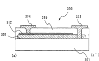
Fig. 3 is the profile that is used to show optical pickocff 300 of the present invention.First electrode 311, light receiving part 302 and second electrode 312 are formed on the plastic 301.First electrode is connected on first electrode tip 313 and second electrode is connected on second electrode tip 314.Interlayer dielectric 315 electric insulations that first electrode 313 and second electrode 314 pass through therebetween.First electrode tip and second electrode tip are the terminals that is used to be connected to the wiring on the wiring substrate.
Under the situation of plastic 301 side incidents, first electrode is formed by conducting film at light, and described conducting film may and be a printing opacity with the semiconductor layer ohmic contact that is formed by silicon.Typically, can adopt ITO (tin indium oxide alloy), indium oxide zinc oxide alloy (In
2O
3-ZnO), zinc oxide (ZnO) and contain the tin indium oxide alloy and the homologue thereof of silica.Moreover second electrode is formed by metal film, described metal film may with the semiconductor layer ohmic contact that forms by silicon.As its representative example, provided and be selected from a kind of element that is included in following group: aluminium (Al), titanium (Ti), chromium (Cr), nickel (Ni), molybdenum (Mo), palladium (Pd), tantalum (Ta), tungsten (W), platinum (Pt), and gold (Au); The alloy material that perhaps comprises 50% this element at least.On the other hand, under the situation of interlayer dielectric side incident, first electrode is formed by metal film at light, this metal film may with the semiconductor layer ohmic contact that forms by silicon.May be used for second electrode with the conducting film of semiconductor layer ohmic contact that forms by silicon and light-permeable.
Remove suppress to degenerate by sealing first electrode 311 and second electrode 312 and light receiving part 302 outside, form described interlayer dielectric 315 and be used for the electrode tip of electric insulation as extraction electrode.Interlayer dielectric can be by organic resin such as acrylic acid, polyimides, polyamide, polyimide amide, and benzocyclobutene, perhaps inorganic material such as silicon oxide film, oxygen silicon nitride membrane, and silicon oxynitride film forms.
In addition, optical pickocff not only can be the structure that cutaway view is showed among Fig. 3, can also be other structure.Fig. 4 A and 4B have showed the cutaway view that is different from the optical pickocff structure that Fig. 3 shows separately.
Fig. 4 A is an example of cutaway view that is used for the light receiving part of display optics transducer 300.Described transducer is by light receiving part 302, form with first electrode tip 313 of light receiving part contact and second electrode 312 and the electrode tip 314 that is connected with second electrode separately.Different with the light receiving part of optical pickocff among Fig. 3, this transducer is first electrode not.Therefore first electrode tip 313 increases with the contact area of light receiving part 302, and then the number of coupling part (contact portion) is preferably very big.In this structure, there is not first electrode, therefore except the quantity that can reduce step, can be improved from the optical transmission rate effect of substrate 301 transmissions.
Fig. 4 B is the example of profile of the light receiving part of display optics transducer.Described transducer is by light receiving part 332, first electrode tip 313 that contacts with light receiving part separately and second electrode 312, and the electrode tip 314 that is connected to second electrode forms.Different with the light receiving part of optical pickocff among Fig. 4 A, light receiving layer is formed on the whole surface of substrate 301, rather than the light receiving layer crossed of composition.Therefore, light receiving layer can not use mask and forms, and does not need to control the position of mask.Therefore, output can improve.
In semiconductor device according to the invention, semiconductor element can be electrically connected to the link (lateral electrode) of insert, and the area that therefore is connected to the wiring substrate increases.That is to say, except that installation strength improves, also available visual inspection connected mode.Therefore, the reliability of technology improves.
In addition, owing to these two parts are bonded on the insert in the mode that whole surface faces with each other by resin, so the connection between semiconductor element and the insert is very firm.Moreover, because semiconductor element and insert interconnect by using resin, therefore can reduce cost.In addition, resin has high set intensity, so can make the semiconductor device with high fracture strength.In addition, form light receiving layer, can form optical pickocff with response characteristic similar to human vision by using amorphous silicon.
[embodiment 1]
By using Fig. 5 A to Fig. 7 D to describe embodiments of the invention.Fig. 5 A, Fig. 5 C, Fig. 6 A, Fig. 6 C, Fig. 7 A and Fig. 7 C show that the top view of substrate and Fig. 5 B, Fig. 5 D, Fig. 6 B, Fig. 6 D, Fig. 7 B and Fig. 7 D are the cutaway views of showing wherein (b)-(b ') zone.
Shown in Fig. 5 A and Fig. 5 B, on plastic 601, form semiconductor film with plasma CVD equipment.Herein, form have p, i and n conduction type separately Si semiconductor film 602 as semiconductor film.Here, have amorphous phase as the I layer of light receiving part, and do not consider the phase of p and n.The illumination range that the film thickness of I layer adapts to required element is arranged in 100-1000nm scope.In the present embodiment, adopt pen film as plastic, forming thickness thereon is the Si semiconductor film of 800nm.
After this, form the contact hole 603 of similarity at predetermined portions in the laser scribing step, purpose is to make the p type silicon fiml in the semiconductor film bottom that forms engage with the metal electrode that forms in the next step as shown in Fig. 5 C and 5D.In this step, preferred scribing stays the p layer of contact hole bottom, be difficult to but control at depth direction by laser, so contact hole may be penetrated into the surface of plastic to guarantee allowance.Therefore correspondingly, actual contact partly is a zonule, and wherein the thickness of p layer is exposed to the wall surface of contact hole, forms in a large number independently the hole to increase contact area.In addition, the focus by adopting light-gathering optics control laser beam is so that defocus wittingly, and the edge of laser beam and the energy density at center can change continuously with mild slope.Under this state, implement laser scribing,, therefore enlarged bigger contact area in the wall surface of scribing part, to produce taper.In the present embodiment, adopt YAG laser, with the frequency of oscillation scanning laser beam of nonoverlapping 1kHz with 1.06 mum wavelengths and 60 μ m beam diameters (φ).
After this, as shown in Fig. 6 A and the 6B, form first electrode 604 and second electrode 605.Formation has the metal conductive film of individual layer or laminated construction as first electrode and second electrode.As film build method, sputtering method, vapor deposition method or galvanoplastic all can adopt, and perhaps adopt said method simultaneously.Under the situation that adopts vapour phase processes such as sputter or vapour deposition, can easily obtain required electrode shape by using metal mask.In metal mask, be formed for two opening portions of an element, and the electrode at the two poles of the earth forms simultaneously.Metal mask, plastic and sheet magnet be with this order setting, with overlapped in sputter equipment, and by with metal mask with the plastic fluid-tight engagement prevents because the electrode area that wraparound (wrap-around) deposited film causes is inhomogeneous.Adopting under the situation of galvanoplastic, on resin, shelter in advance by in the zone that does not need metal electrode, carrying out silk screen printing, after forming metal electrode by peeling off the electrode shape of acquisition needs.Form first electrode and second electrode 604 and 605 of thickness in 0.5-100 mu m ranges under these conditions.
In the present embodiment, use metal mask to utilize sputtering method to make the Ni metal deposition.The thickness of metal mask is 0.1mm, is formed by nickel.Under the situation that metal mask and plastic are combined closely mutually by the sheet magnet, described metal mask and plastic are arranged in the sputter equipment.Utilizing diameter is that 6 inches, purity are 99.99% Ni target, discharging in by the argon gas atmosphere at 1.0Pa under with the RF output of 1.0kW by sputter, has formed by nickel and has formed the thick film of 1.5 μ m.
After this, as shown in Fig. 6 C and Fig. 6 D, form dielectric film 606, wherein the part of first electrode 604 and second electrode 605 exposes and opening separately.Adopt silk screen print method to form dielectric film.Alternately, described dielectric film can form on the whole surface of substrate by CVD method or coating process, after this, but an etching part wherein forming contact hole, thereby expose each electrode, electrode 604 and 605 just.By leaving contact hole symmetrically, can prevent optical pickocff be assembled to the wiring substrate on the time run-off the straight.
In contact hole, form electrode tip 607 and 608, wherein expose the part of electrode 604 and 605 respectively as extraction electrode.Described electrode tip can form by containing the conducting film of metallic element as silver, gold, copper, platinum or nickel.In the present embodiment, form 1.35 * 1.8mm
2Extraction electrode.In the present embodiment, use the resin glue that contains copper to form electrode tip with silk screen printing.
After this, as shown in Figure 7A and 7B, anisotropic-electroconductive adhesive 609 is coated on the whole surface of substrate.In the present embodiment, applied the epoxy resin that is dispersed with silver particles.It should be noted that in the present embodiment, anisotropic-electroconductive adhesive is coated on the substrate by coating process, but print process, particularly silk screen print method can be used to substitute this step.Under the situation of using silk screen print method, thereby because anisotropic-electroconductive adhesive is to place by the removal scribe line to cut away optical pickocff afterwards, so when the scribing substrate, adhesive can't hinder.
After this, as shown in Fig. 7 C and 7D, the insert 613 that forms link (lateral electrode) 611 and 612 is placed on the anisotropic-electroconductive adhesive.At this moment, aim at and be provided with insert 613, so that the electrode tip of optical pickocff 607 and 608 is in the face of being formed at the link (lateral electrode) 611 and 612 in the insert.Insert joins on the substrate in arrow 614 directions by hot press.
After this, by the laser scribing step optical pickocff is cut away.In the present embodiment, laser radiation is at the minor axis that is parallel to optical pickocff and do not form optical sensor element (A axle: on zone 621a to 621d), with vertical (just with the optical pickocff minor axis, the major axis that is parallel to optical pickocff) and not form optical sensor element (B axle: on zone 622a to 622e), to cut away optical pickocff.In the present embodiment, the employing frequency of oscillation is 1kHz, and wavelength is that 1.06 μ m and beam diameter (φ) are the YAG laser illumination of 60 μ m.
Described optical pickocff can form by above-mentioned steps.
In semiconductor device according to the invention, semiconductor element can be electrically connected to the link (lateral electrode) of insert, and the area that therefore is connected to the wiring substrate increases.That is to say, except that installation strength improves, also available visual inspection connected mode.Therefore, the reliability of technology improves.Moreover described semiconductor element is formed on the substrate, and Substrate Area and as the zone of semiconductor element about equally.Therefore, can be integrated into the semiconductor device height on wiring substrate or the homologue.
Moreover, owing to these two parts engage in the mode that whole surface faces with each other, so being connected of semiconductor element and insert is very firm.In addition, because semiconductor element and insert are connected to one another by resin, therefore can reduce cost.In addition, resin has high set intensity, so can make the semiconductor device with high fracture strength.
[embodiment 2]
Can be by making different electronic equipments in conjunction with semiconductor device according to the invention.Such electronic equipment comprises, cellular phone, laptop PC, game machine, car navigation device, portable voice frequency equipment, hand-held AV equipment, digital camera, film camera, instant camera, room conditioning, car air-conditioner, heating ventilation and air-conditioning equipment, electronics kettle, CRT type projection TV, lighting apparatus, lighting device, and similar products.After this instantiation of electronic equipment will illustrate.
Optical pickocff of the present invention can be used for cellular phone, laptop PC, and digital camera, game machine, car navigation device, portable voice frequency equipment and similar products as the transducer that is used for optimally regulating display and backlight illumination, and are saved battery.The battery of solar cell as these equipment can be provided.Described semiconductor device can be reduced in size and highly integrated, and can make the size of electronic equipment littler by using them.
Optical pickocff of the present invention can be used for the key switch of cellular phone and the transducer that hand-held AV equipment is used to control the Kai Heguan of LED backlight and cold-cathode tube or is used for conserve batteries as transducer.By providing transducer, in bright light environments, switch cuts out, can reduce long-term push-button battery consumption.Therefore because semiconductor device of the present invention can be reduced in size and highly integrated, can obtain the electronic equipment of the littler and energy efficient of size.
In addition, optical pickocff of the present invention can be used as the transducer of flash of light dimmer control or the transducer of aperture control is used for digital camera, film camera, instant camera.In addition, solar cell can be used as battery and is used for these electronic equipments.Because described semiconductor device can be reduced in size and highly integrated, and thus can be littler by the size of using their electronic equipments.
Moreover optical pickocff of the present invention can be used as the transducer of control air-flow or temperature, is used for room conditioning, car air-conditioner and ventilation and air-conditioning equipment.Therefore because semiconductor device of the present invention can be reduced in size and highly integrated, can obtain the electronic equipment of the littler and energy efficient of size.
Moreover optical pickocff of the present invention can be used as and is used to control the transducer of temperature with insulation, is used for the electronics kettle.After indoor lamp is closed, can holding temperature be established low by optical pickocff of the present invention.Because optical pickocff is little and thin, it can be provided on the desired position.Therefore, can reach the purpose of saves energy.
Optical pickocff of the present invention can be used as the transducer of regulating scan line position (position of RGB scan line (digital AF)), is used for the display of CRT type projection TV.Because semiconductor device of the present invention can be reduced in size and highly integrated, can further reduce the size of electronic equipment by using it, and can desired location provide transducer.In addition, make the High-Speed Automatic adjusting of CRT type projection TV become possibility.
Optical pickocff of the present invention can be used as the transducer that control lighting apparatus of all kinds and lighting device are opened and closed, and is used for home lighting equipment miscellaneous, outside light, street lamp, unwatched public utility, sports ground, automobile, calculator and similar facilities.But by transducer saves energy of the present invention.By adopting solar cell according to the present invention as the battery that is used for this electronic equipment, but the battery attenuation is to reduce the size of electronic equipment.
It is 2003-347678 Japanese publication at the sequence number of Japan Patent office application that the present invention is based on October 6th, 2003, and the content of described application is incorporated herein by reference herein.
Claims (46)
1. semiconductor device comprises:
First substrate;
Second substrate;
Be formed on the semiconductor element on described first substrate; With
Be formed on the conducting film of described second edges of substrate part,
A face of wherein said first substrate and a face of described second substrate interfix by the bonding connection parts, and
Wherein said semiconductor element is electrically connected to described conducting film by described bonding connection parts.
2. semiconductor device comprises:
Semiconductor element;
First substrate wherein forms first link that is electrically connected with this semiconductor element;
Second substrate; With
Be formed on second link of described second edges of substrate part,
Wherein said semiconductor element and described second substrate are bonded with each other by the bonding connection parts, and described first link and the electrical connection of described second link, and
Wherein said semiconductor element is electrically connected to described second link by described bonding connection parts.
3. semiconductor device as claimed in claim 1,
Wherein said bonding connection parts are anisotropic-electroconductive adhesive or anisotropic conductive film.
4. semiconductor device as claimed in claim 2,
Wherein said bonding connection parts are anisotropic-electroconductive adhesive or anisotropic conductive film.
5. semiconductor device as claimed in claim 2,
Wherein said first link is electrically connected to described second link by the conducting particles that is included in the described bonding connection parts.
6. semiconductor device as claimed in claim 1,
Wherein said first substrate is that thickness is 0.1 to 1mm substrate, membranaceous substrate, perhaps sheet-like substrates.
7. semiconductor device as claimed in claim 2,
Wherein said first substrate is that thickness is 0.1 to 1mm substrate, membranaceous substrate, perhaps sheet-like substrates.
8. semiconductor device as claimed in claim 1,
Wherein said first substrate is a dielectric substrate.
9. semiconductor device as claimed in claim 2,
Wherein said first substrate is a dielectric substrate.
10. semiconductor device as claimed in claim 1,
Wherein said first substrate is glass substrate or the substrate that formed by organic resin.
11. semiconductor device as claimed in claim 2,
Wherein said first substrate is glass substrate or the substrate that formed by organic resin.
12. semiconductor device as claimed in claim 1,
Wherein said semiconductor element has the layer that is formed by semi-conducting material.
13. semiconductor device as claimed in claim 2,
Wherein said semiconductor element has the layer that is formed by semi-conducting material.
14. semiconductor device as claimed in claim 1,
Wherein said semiconductor element has thin-film transistor or diode.
15. semiconductor device as claimed in claim 2,
Wherein said semiconductor element has thin-film transistor or diode.
16. semiconductor device as claimed in claim 1,
Wherein said semiconductor element has thin-film transistor and diode.
17. semiconductor device as claimed in claim 2,
Wherein said semiconductor element has thin-film transistor and diode.
18. semiconductor device as claimed in claim 1,
Wherein said semiconductor device is an optical pickocff, optical-electrical converter, perhaps solar cell.
19. semiconductor device as claimed in claim 2,
Wherein said semiconductor device is an optical pickocff, optical-electrical converter, perhaps solar cell.
20. semiconductor device as claimed in claim 1,
Wherein said semiconductor device is the integrated circuit that is formed by thin-film transistor.
21. semiconductor device as claimed in claim 2,
Wherein said semiconductor device is the integrated circuit that is formed by thin-film transistor.
22. have the electronic equipment of semiconductor device as claimed in claim 1, wherein said electronic equipment is selected from the group that comprises following equipment: cellular phone, laptop PC, game machine, car navigation device, portable voice frequency equipment, hand-held AV equipment, camera, air-conditioning, heating ventilation and air-conditioning equipment, electronics kettle, CRT type projection TV, lighting apparatus and lighting device.
23. have the electronic equipment of semiconductor device as claimed in claim 2, wherein said electronic equipment is selected from the group that comprises following equipment: cellular phone, laptop PC, game machine, car navigation device, portable voice frequency equipment, hand-held AV equipment, camera, air-conditioning, heating ventilation and air-conditioning equipment, electronics kettle, CRT type projection TV, lighting apparatus and lighting device.
24. a semiconductor device comprises:
First substrate;
Second substrate;
Be formed on the semiconductor element on described first substrate; With
Conducting film, its each all be formed at least one face of described second substrate,
A face of wherein said first substrate and a face of described second substrate interfix by the bonding connection parts, and
Wherein said semiconductor element is electrically connected to described conducting film by described bonding connection parts.
25. a semiconductor device comprises:
Semiconductor element;
First substrate forms first link that is electrically connected with described semiconductor element therein;
Second substrate; With
Be formed on second link at least one face of described second substrate,
Wherein said semiconductor element and described second substrate are bonded with each other by the bonding connection parts, and described first link is electrically connected to described second link by these bonding connection parts, and
Wherein said semiconductor element is electrically connected to described second link by described bonding connection parts.
26. semiconductor device as claimed in claim 24,
Wherein said bonding connection parts are anisotropic-electroconductive adhesive or anisotropic conductive film.
27. semiconductor device as claimed in claim 25,
Wherein said bonding connection parts are anisotropic-electroconductive adhesive or anisotropic conductive film.
28. semiconductor device as claimed in claim 25,
Wherein said first link is electrically connected to described second link by the conducting particles that is included in the described bonding connection parts.
29. semiconductor device as claimed in claim 24,
Wherein said first substrate is that thickness is 0.1 to 1mm substrate, membranaceous substrate, perhaps sheet-like substrates.
30. semiconductor device as claimed in claim 25,
Wherein said first substrate is that thickness is 0.1 to 1mm substrate, membranaceous substrate, perhaps sheet-like substrates.
31. semiconductor device as claimed in claim 24,
Wherein said first substrate is a dielectric substrate.
32. semiconductor device as claimed in claim 25,
Wherein said first substrate is a dielectric substrate.
33. semiconductor device as claimed in claim 24,
Wherein said first substrate is glass substrate or the substrate that formed by organic resin.
34. semiconductor device as claimed in claim 25,
Wherein said first substrate is glass substrate or the substrate that formed by organic resin.
35. semiconductor device as claimed in claim 24,
Wherein said semiconductor element has the layer that is formed by semi-conducting material.
36. semiconductor device as claimed in claim 25,
Wherein said semiconductor element has the layer that is formed by semi-conducting material.
37. semiconductor device as claimed in claim 24,
Wherein said semiconductor element has thin-film transistor or diode.
38. semiconductor device as claimed in claim 25,
Wherein said semiconductor element has thin-film transistor or diode.
39. semiconductor device as claimed in claim 24,
Wherein said semiconductor element has thin-film transistor and diode.
40. semiconductor device as claimed in claim 25,
Wherein said semiconductor element has thin-film transistor and diode.
41. semiconductor device as claimed in claim 24,
Wherein said semiconductor device is optical pickocff, optical-electrical converter, perhaps solar cell.
42. semiconductor device as claimed in claim 25,
Wherein said semiconductor device is optical pickocff, optical-electrical converter, perhaps solar cell.
43. semiconductor device as claimed in claim 24,
Wherein said semiconductor device is the integrated circuit that is formed by thin-film transistor.
44. semiconductor device as claimed in claim 25,
Wherein said semiconductor device is the integrated circuit that is formed by thin-film transistor.
45. have the electronic equipment of semiconductor device as claimed in claim 24, wherein said electronic equipment is selected from the group that comprises following equipment: cellular phone, laptop PC, game machine, car navigation device, portable voice frequency equipment, hand-held AV equipment, camera, air-conditioning, heating ventilation and air-conditioning equipment, electronics kettle, CRT type projection TV, lighting apparatus and lighting device.
46. have the electronic equipment of semiconductor device as claimed in claim 25, wherein said electronic equipment is selected from the group that comprises following equipment: cellular phone, laptop PC, game machine, car navigation device, portable voice frequency equipment, hand-held AV equipment, camera, air-conditioning, heating ventilation and air-conditioning equipment, electronics kettle, CRT type projection TV, lighting apparatus and lighting device.
Applications Claiming Priority (3)
| Application Number | Priority Date | Filing Date | Title |
|---|---|---|---|
| JP347678/03 | 2003-10-06 | ||
| JP2003347678 | 2003-10-06 | ||
| JP347678/2003 | 2003-10-06 |
Publications (2)
| Publication Number | Publication Date |
|---|---|
| CN1606169A CN1606169A (en) | 2005-04-13 |
| CN100499175C true CN100499175C (en) | 2009-06-10 |
Family
ID=34509704
Family Applications (1)
| Application Number | Title | Priority Date | Filing Date |
|---|---|---|---|
| CNB2004100874789A Expired - Fee Related CN100499175C (en) | 2003-10-06 | 2004-10-08 | Semiconductor device and method for manufacturing the same |
Country Status (5)
| Country | Link |
|---|---|
| US (2) | US7180197B2 (en) |
| EP (1) | EP1542272B1 (en) |
| JP (1) | JP4679106B2 (en) |
| KR (2) | KR20050033434A (en) |
| CN (1) | CN100499175C (en) |
Families Citing this family (36)
| Publication number | Priority date | Publication date | Assignee | Title |
|---|---|---|---|---|
| JP2005340647A (en) * | 2004-05-28 | 2005-12-08 | Nec Compound Semiconductor Devices Ltd | Interposer substrate, semiconductor package, semiconductor device, and method for manufacturing them |
| JP2006202938A (en) * | 2005-01-20 | 2006-08-03 | Kojiro Kobayashi | Semiconductor device and its manufacturing method |
| WO2006082909A1 (en) * | 2005-02-03 | 2006-08-10 | Matsushita Electric Industrial Co., Ltd. | Flip chip mounting body and method for mounting such flip chip mounting body and bump forming method |
| US7994021B2 (en) * | 2006-07-28 | 2011-08-09 | Semiconductor Energy Laboratory Co., Ltd. | Method of manufacturing semiconductor device |
| US7943287B2 (en) * | 2006-07-28 | 2011-05-17 | Semiconductor Energy Laboratory Co., Ltd. | Method for manufacturing display device |
| KR101346246B1 (en) | 2006-08-24 | 2013-12-31 | 가부시키가이샤 한도오따이 에네루기 켄큐쇼 | Method for manufacturing display device |
| US7795154B2 (en) | 2006-08-25 | 2010-09-14 | Semiconductor Energy Laboratory Co., Ltd. | Method for manufacturing semiconductor device that uses laser ablation, to selectively remove one or more material layers |
| US8563431B2 (en) * | 2006-08-25 | 2013-10-22 | Semiconductor Energy Laboratory Co., Ltd. | Method for manufacturing semiconductor device |
| US7651896B2 (en) * | 2006-08-30 | 2010-01-26 | Semiconductor Energy Laboratory Co., Ltd. | Method for manufacturing semiconductor device |
| JP5110830B2 (en) * | 2006-08-31 | 2012-12-26 | 株式会社半導体エネルギー研究所 | Method for manufacturing semiconductor device |
| US7960261B2 (en) * | 2007-03-23 | 2011-06-14 | Semiconductor Energy Laboratory Co., Ltd. | Method for manufacturing crystalline semiconductor film and method for manufacturing thin film transistor |
| KR101423055B1 (en) * | 2007-04-18 | 2014-07-25 | 가부시키가이샤 한도오따이 에네루기 켄큐쇼 | Photoelectric conversion element having a semiconductor and semiconductor device using the same |
| EP1986238A3 (en) * | 2007-04-27 | 2010-12-29 | Semiconductor Energy Laboratory Co., Ltd. | Resin molded optical semiconductor device and corresponding fabrication method |
| JP4989549B2 (en) * | 2007-08-24 | 2012-08-01 | 三洋電機株式会社 | Solar cell and solar cell module |
| KR100898503B1 (en) | 2007-09-04 | 2009-05-20 | 주식회사 아이에스시테크놀러지 | Interposer for high frequency |
| JP5252472B2 (en) | 2007-09-28 | 2013-07-31 | シャープ株式会社 | Solar cell, method for manufacturing solar cell, method for manufacturing solar cell module, and solar cell module |
| US20100263718A1 (en) | 2007-11-09 | 2010-10-21 | Yoshiya Abiko | Solar cell module and method for manufacturing solar cell module |
| DE102007055017B4 (en) * | 2007-11-14 | 2010-11-04 | Fraunhofer-Gesellschaft zur Förderung der angewandten Forschung e.V. | Method for connecting two joining surfaces and component with two joining surfaces joined |
| KR20100093590A (en) * | 2007-12-17 | 2010-08-25 | 퀄컴 엠이엠스 테크놀로지스, 인크. | Photovoltaics with interferometric back side masks |
| US20090278213A1 (en) * | 2008-05-08 | 2009-11-12 | International Business Machines Corporation | Electrode arrays and methods of fabricating the same using printing plates to arrange particles in an array |
| US8207487B2 (en) * | 2008-06-25 | 2012-06-26 | Semiconductor Energy Laboratory Co., Ltd. | Photoelectric conversion device including charge/discharge circuit |
| EP2448008A1 (en) * | 2009-06-22 | 2012-05-02 | Sharp Kabushiki Kaisha | Solar cell, solar cell with wiring sheet attached, and solar cell module |
| WO2011001883A1 (en) | 2009-06-29 | 2011-01-06 | シャープ株式会社 | Wiring sheet, solar cell with wiring sheet, solar cell module and wiring sheet roll |
| CN102484150A (en) * | 2009-08-27 | 2012-05-30 | 独立行政法人产业技术综合研究所 | Multi-junction photoelectric converter, integrated multi-junction photoelectric converter, and method for manufacturing same |
| JP5660122B2 (en) * | 2010-03-02 | 2015-01-28 | コニカミノルタ株式会社 | Radiation detection panel, radiation image detector, method for manufacturing radiation detection panel, and method for manufacturing radiation image detector |
| DE102010027953A1 (en) * | 2010-04-20 | 2011-12-01 | Robert Bosch Gmbh | Method for producing a photovoltaic module with back-contacted semiconductor cells and photovoltaic module |
| JP2012080085A (en) * | 2010-09-10 | 2012-04-19 | Nichia Chem Ind Ltd | Support medium and light emitting device using the same |
| CN102810574A (en) * | 2011-05-31 | 2012-12-05 | 联景光电股份有限公司 | Electrode of solar cell |
| CN102569247A (en) * | 2012-01-17 | 2012-07-11 | 华为终端有限公司 | Integrated module, integrated system board and electronic equipment |
| US9184211B2 (en) | 2012-07-05 | 2015-11-10 | Semiconductor Energy Laboratory Co., Ltd. | Light-emitting device and method for fabricating the same |
| KR102173801B1 (en) | 2012-07-12 | 2020-11-04 | 가부시키가이샤 한도오따이 에네루기 켄큐쇼 | Display device and method for manufacturing display device |
| US11074025B2 (en) | 2012-09-03 | 2021-07-27 | Semiconductor Energy Laboratory Co., Ltd. | Display device and method for manufacturing the same |
| US11581446B2 (en) * | 2015-10-08 | 2023-02-14 | The Boeing Company | Semiconductor device including an electrically conductive adhesive layer and a bypass diode in a carrier |
| US10879211B2 (en) | 2016-06-30 | 2020-12-29 | R.S.M. Electron Power, Inc. | Method of joining a surface-mount component to a substrate with solder that has been temporarily secured |
| JP2018098487A (en) * | 2016-12-14 | 2018-06-21 | 株式会社村田製作所 | Semiconductor module |
| KR102423292B1 (en) * | 2021-09-07 | 2022-07-20 | 한국기계연구원 | Etching apparatus and interposer manufacturing system including the same |
Citations (1)
| Publication number | Priority date | Publication date | Assignee | Title |
|---|---|---|---|---|
| US4423435A (en) * | 1980-10-27 | 1983-12-27 | Texas Instruments Incorporated | Assembly of an electronic device on an insulative substrate |
Family Cites Families (40)
| Publication number | Priority date | Publication date | Assignee | Title |
|---|---|---|---|---|
| JPS63122133A (en) * | 1986-11-11 | 1988-05-26 | Matsushita Electric Ind Co Ltd | Electrically connecting method for semiconductor chip |
| JPH0287558A (en) * | 1988-09-24 | 1990-03-28 | Murata Mfg Co Ltd | Ic chip |
| WO1990004263A1 (en) * | 1988-10-14 | 1990-04-19 | Matsushita Electric Industrial Co., Ltd. | Image sensor and method of producing the same |
| US5272376A (en) * | 1990-06-01 | 1993-12-21 | Clarion Co., Ltd. | Electrode structure for a semiconductor device |
| JPH04107955A (en) * | 1990-08-28 | 1992-04-09 | Matsushita Electric Ind Co Ltd | Sealing method of electronic circuit element |
| JP3329512B2 (en) | 1993-03-22 | 2002-09-30 | 株式会社半導体エネルギー研究所 | Semiconductor circuit and manufacturing method thereof |
| US5501989A (en) | 1993-03-22 | 1996-03-26 | Semiconductor Energy Laboratory Co., Ltd. | Method of making semiconductor device/circuit having at least partially crystallized semiconductor layer |
| JP3164182B2 (en) * | 1993-08-27 | 2001-05-08 | 株式会社村田製作所 | Composite electronic components |
| JP3150840B2 (en) | 1994-03-11 | 2001-03-26 | 株式会社半導体エネルギー研究所 | Method for manufacturing semiconductor device |
| US6700133B1 (en) * | 1994-03-11 | 2004-03-02 | Semiconductor Energy Laboratory Co., Ltd. | Method for producing semiconductor device |
| US5672545A (en) * | 1994-08-08 | 1997-09-30 | Santa Barbara Research Center | Thermally matched flip-chip detector assembly and method |
| JP2900229B2 (en) | 1994-12-27 | 1999-06-02 | 株式会社半導体エネルギー研究所 | Semiconductor device, manufacturing method thereof, and electro-optical device |
| JPH08201540A (en) * | 1995-01-31 | 1996-08-09 | Citizen Watch Co Ltd | Structure of watch with solar cell |
| KR19990028493A (en) * | 1995-06-30 | 1999-04-15 | 니시무로 타이죠 | Electronic component and method of production thereof |
| JPH0945805A (en) * | 1995-07-31 | 1997-02-14 | Fujitsu Ltd | Wiring board, semiconductor device, method for removing the semiconductor device from wiring board, and manufacture of semiconductor device |
| JP3183390B2 (en) * | 1995-09-05 | 2001-07-09 | キヤノン株式会社 | Photoelectric conversion device and imaging device using the same |
| JPH1022329A (en) * | 1996-07-01 | 1998-01-23 | Mitsui High Tec Inc | Semiconductor device |
| US6461890B1 (en) * | 1996-12-27 | 2002-10-08 | Rohm Co., Ltd. | Structure of semiconductor chip suitable for chip-on-board system and methods of fabricating and mounting the same |
| US5783465A (en) * | 1997-04-03 | 1998-07-21 | Lucent Technologies Inc. | Compliant bump technology |
| JP3856250B2 (en) * | 1997-04-23 | 2006-12-13 | シチズン電子株式会社 | SMD type LED |
| KR100539060B1 (en) * | 1997-10-28 | 2007-04-25 | 소니 케미카루 가부시키가이샤 | Anisotropic conductive adhesive and adhesive film |
| SG71734A1 (en) * | 1997-11-21 | 2000-04-18 | Inst Materials Research & Eng | Area array stud bump flip chip and assembly process |
| JP4085459B2 (en) * | 1998-03-02 | 2008-05-14 | セイコーエプソン株式会社 | Manufacturing method of three-dimensional device |
| JP3561166B2 (en) * | 1999-01-21 | 2004-09-02 | 株式会社リコー | Method for connecting electronic components using anisotropic conductive paste |
| JP2000323472A (en) * | 1999-05-06 | 2000-11-24 | Canon Inc | Semicondcutor device, photoelectric converter and manufactuer thereof |
| US6879014B2 (en) | 2000-03-20 | 2005-04-12 | Aegis Semiconductor, Inc. | Semitransparent optical detector including a polycrystalline layer and method of making |
| JP3597754B2 (en) * | 2000-04-24 | 2004-12-08 | Necエレクトロニクス株式会社 | Semiconductor device and manufacturing method thereof |
| JP2001358437A (en) * | 2000-06-15 | 2001-12-26 | Seiko Epson Corp | Method for mounting semiconductor device |
| JP2002094082A (en) | 2000-07-11 | 2002-03-29 | Seiko Epson Corp | Optical element and its manufacturing method and electronic equipment |
| US6624921B1 (en) * | 2001-03-12 | 2003-09-23 | Amkor Technology, Inc. | Micromirror device package fabrication method |
| JP2002313979A (en) * | 2001-04-09 | 2002-10-25 | Sony Corp | Interposer and electronic circuit device |
| JP2003045236A (en) | 2001-08-03 | 2003-02-14 | Nec Kagoshima Ltd | Anisotropy conductive film and connection method of integrated circuit device |
| JP2003060744A (en) | 2001-08-21 | 2003-02-28 | Sanyo Electric Co Ltd | Portable device |
| JP4000507B2 (en) | 2001-10-04 | 2007-10-31 | ソニー株式会社 | Method for manufacturing solid-state imaging device |
| US6555917B1 (en) * | 2001-10-09 | 2003-04-29 | Amkor Technology, Inc. | Semiconductor package having stacked semiconductor chips and method of making the same |
| JP5030360B2 (en) * | 2002-12-25 | 2012-09-19 | オリンパス株式会社 | Method for manufacturing solid-state imaging device |
| JP3972825B2 (en) | 2003-01-28 | 2007-09-05 | セイコーエプソン株式会社 | Manufacturing method of active matrix display device |
| JP2004266271A (en) * | 2003-02-12 | 2004-09-24 | Matsushita Electric Ind Co Ltd | Electronic part mounting body and method for manufacturing the same |
| US20040156177A1 (en) | 2003-02-12 | 2004-08-12 | Matsushita Electric Industrial Co., Ltd. | Package of electronic components and method for producing the same |
| JP3693060B2 (en) * | 2003-09-24 | 2005-09-07 | セイコーエプソン株式会社 | Semiconductor device and manufacturing method thereof, circuit board, and electronic apparatus |
-
2004
- 2004-09-15 EP EP04021934.7A patent/EP1542272B1/en not_active Not-in-force
- 2004-09-29 US US10/951,811 patent/US7180197B2/en active Active
- 2004-09-30 KR KR1020040077760A patent/KR20050033434A/en active Search and Examination
- 2004-10-05 JP JP2004292650A patent/JP4679106B2/en not_active Expired - Fee Related
- 2004-10-08 CN CNB2004100874789A patent/CN100499175C/en not_active Expired - Fee Related
-
2006
- 2006-08-03 US US11/498,164 patent/US8481370B2/en active Active
-
2009
- 2009-09-02 KR KR1020090082612A patent/KR20090114343A/en active Search and Examination
Patent Citations (1)
| Publication number | Priority date | Publication date | Assignee | Title |
|---|---|---|---|---|
| US4423435A (en) * | 1980-10-27 | 1983-12-27 | Texas Instruments Incorporated | Assembly of an electronic device on an insulative substrate |
Also Published As
| Publication number | Publication date |
|---|---|
| US8481370B2 (en) | 2013-07-09 |
| CN1606169A (en) | 2005-04-13 |
| KR20050033434A (en) | 2005-04-12 |
| KR20090114343A (en) | 2009-11-03 |
| JP2005175436A (en) | 2005-06-30 |
| US7180197B2 (en) | 2007-02-20 |
| EP1542272A3 (en) | 2012-03-07 |
| JP4679106B2 (en) | 2011-04-27 |
| EP1542272A2 (en) | 2005-06-15 |
| US20050082655A1 (en) | 2005-04-21 |
| EP1542272B1 (en) | 2016-07-20 |
| US20060270114A1 (en) | 2006-11-30 |
Similar Documents
| Publication | Publication Date | Title |
|---|---|---|
| CN100499175C (en) | Semiconductor device and method for manufacturing the same | |
| CN100594618C (en) | Semiconductor device and method for manufacturing the same | |
| TWI651202B (en) | Illuminating device | |
| CN101375412B (en) | In solder covered copper foil ribbon conductor wire and its connection method | |
| CN101086326B (en) | Luminescent diode lighting circuit, lighting device and liquid crystal display device | |
| JP2002057358A (en) | Photovoltaic element, its manufacturing method, method for removing coating of insulated wire, and method for joining the insulated wire to conductor | |
| US7994709B2 (en) | OLED device employing a metal thin-film connected to a high-current cable | |
| CN102598301A (en) | Solar cell and manufacturing method thereof | |
| CN110299376B (en) | Display device | |
| JP4481135B2 (en) | Semiconductor device and manufacturing method thereof | |
| US20020197917A1 (en) | Conductor connection method, conductor connection structure, and solar cell module having connection structure | |
| US8247247B2 (en) | Method of manufacturing LED module | |
| US20090090544A1 (en) | System and Method for Substrate with Interconnects and Sealing Surface | |
| JP2008294414A (en) | Semiconductor device and method for fabricating same | |
| JP4427843B2 (en) | Electronic component and manufacturing method thereof | |
| CN208655666U (en) | A kind of solar cell module | |
| JP3484852B2 (en) | Solar cell manufacturing method | |
| CN117012799A (en) | Driving backboard and display panel | |
| CN115719743A (en) | Display panel, preparation method thereof and display device | |
| JPH08236794A (en) | Manufacture of thin-film solar cell module | |
| CN116608449A (en) | Light bar assembly and manufacturing method thereof |
Legal Events
| Date | Code | Title | Description |
|---|---|---|---|
| C06 | Publication | ||
| PB01 | Publication | ||
| C10 | Entry into substantive examination | ||
| SE01 | Entry into force of request for substantive examination | ||
| C14 | Grant of patent or utility model | ||
| GR01 | Patent grant | ||
| CF01 | Termination of patent right due to non-payment of annual fee | ||
| CF01 | Termination of patent right due to non-payment of annual fee |
Granted publication date: 20090610 Termination date: 20211008 |