CN100505170C - Proximity head heating method and apparatus - Google Patents
Proximity head heating method and apparatus Download PDFInfo
- Publication number
- CN100505170C CN100505170C CNB200510063774XA CN200510063774A CN100505170C CN 100505170 C CN100505170 C CN 100505170C CN B200510063774X A CNB200510063774X A CN B200510063774XA CN 200510063774 A CN200510063774 A CN 200510063774A CN 100505170 C CN100505170 C CN 100505170C
- Authority
- CN
- China
- Prior art keywords
- fluid
- heating part
- head
- heating
- passage
- Prior art date
- Legal status (The legal status is an assumption and is not a legal conclusion. Google has not performed a legal analysis and makes no representation as to the accuracy of the status listed.)
- Expired - Fee Related
Links
Images


Classifications
-
- H—ELECTRICITY
- H01—ELECTRIC ELEMENTS
- H01L—SEMICONDUCTOR DEVICES NOT COVERED BY CLASS H10
- H01L21/00—Processes or apparatus adapted for the manufacture or treatment of semiconductor or solid state devices or of parts thereof
- H01L21/67—Apparatus specially adapted for handling semiconductor or electric solid state devices during manufacture or treatment thereof; Apparatus specially adapted for handling wafers during manufacture or treatment of semiconductor or electric solid state devices or components ; Apparatus not specifically provided for elsewhere
- H01L21/67005—Apparatus not specifically provided for elsewhere
- H01L21/67011—Apparatus for manufacture or treatment
- H01L21/67017—Apparatus for fluid treatment
- H01L21/67023—Apparatus for fluid treatment for general liquid treatment, e.g. etching followed by cleaning
-
- H—ELECTRICITY
- H01—ELECTRIC ELEMENTS
- H01L—SEMICONDUCTOR DEVICES NOT COVERED BY CLASS H10
- H01L21/00—Processes or apparatus adapted for the manufacture or treatment of semiconductor or solid state devices or of parts thereof
- H01L21/02—Manufacture or treatment of semiconductor devices or of parts thereof
- H01L21/04—Manufacture or treatment of semiconductor devices or of parts thereof the devices having at least one potential-jump barrier or surface barrier, e.g. PN junction, depletion layer or carrier concentration layer
- H01L21/18—Manufacture or treatment of semiconductor devices or of parts thereof the devices having at least one potential-jump barrier or surface barrier, e.g. PN junction, depletion layer or carrier concentration layer the devices having semiconductor bodies comprising elements of Group IV of the Periodic System or AIIIBV compounds with or without impurities, e.g. doping materials
- H01L21/30—Treatment of semiconductor bodies using processes or apparatus not provided for in groups H01L21/20 - H01L21/26
-
- B—PERFORMING OPERATIONS; TRANSPORTING
- B08—CLEANING
- B08B—CLEANING IN GENERAL; PREVENTION OF FOULING IN GENERAL
- B08B3/00—Cleaning by methods involving the use or presence of liquid or steam
- B08B3/02—Cleaning by the force of jets or sprays
-
- C—CHEMISTRY; METALLURGY
- C25—ELECTROLYTIC OR ELECTROPHORETIC PROCESSES; APPARATUS THEREFOR
- C25D—PROCESSES FOR THE ELECTROLYTIC OR ELECTROPHORETIC PRODUCTION OF COATINGS; ELECTROFORMING; APPARATUS THEREFOR
- C25D17/00—Constructional parts, or assemblies thereof, of cells for electrolytic coating
- C25D17/001—Apparatus specially adapted for electrolytic coating of wafers, e.g. semiconductors or solar cells
-
- H—ELECTRICITY
- H01—ELECTRIC ELEMENTS
- H01L—SEMICONDUCTOR DEVICES NOT COVERED BY CLASS H10
- H01L21/00—Processes or apparatus adapted for the manufacture or treatment of semiconductor or solid state devices or of parts thereof
- H01L21/67—Apparatus specially adapted for handling semiconductor or electric solid state devices during manufacture or treatment thereof; Apparatus specially adapted for handling wafers during manufacture or treatment of semiconductor or electric solid state devices or components ; Apparatus not specifically provided for elsewhere
- H01L21/67005—Apparatus not specifically provided for elsewhere
- H01L21/67011—Apparatus for manufacture or treatment
- H01L21/67017—Apparatus for fluid treatment
- H01L21/67028—Apparatus for fluid treatment for cleaning followed by drying, rinsing, stripping, blasting or the like
- H01L21/6704—Apparatus for fluid treatment for cleaning followed by drying, rinsing, stripping, blasting or the like for wet cleaning or washing
- H01L21/67051—Apparatus for fluid treatment for cleaning followed by drying, rinsing, stripping, blasting or the like for wet cleaning or washing using mainly spraying means, e.g. nozzles
-
- H—ELECTRICITY
- H01—ELECTRIC ELEMENTS
- H01L—SEMICONDUCTOR DEVICES NOT COVERED BY CLASS H10
- H01L21/00—Processes or apparatus adapted for the manufacture or treatment of semiconductor or solid state devices or of parts thereof
- H01L21/67—Apparatus specially adapted for handling semiconductor or electric solid state devices during manufacture or treatment thereof; Apparatus specially adapted for handling wafers during manufacture or treatment of semiconductor or electric solid state devices or components ; Apparatus not specifically provided for elsewhere
- H01L21/67005—Apparatus not specifically provided for elsewhere
- H01L21/67011—Apparatus for manufacture or treatment
- H01L21/67017—Apparatus for fluid treatment
- H01L21/67063—Apparatus for fluid treatment for etching
- H01L21/67075—Apparatus for fluid treatment for etching for wet etching
- H01L21/6708—Apparatus for fluid treatment for etching for wet etching using mainly spraying means, e.g. nozzles
-
- H—ELECTRICITY
- H01—ELECTRIC ELEMENTS
- H01L—SEMICONDUCTOR DEVICES NOT COVERED BY CLASS H10
- H01L21/00—Processes or apparatus adapted for the manufacture or treatment of semiconductor or solid state devices or of parts thereof
- H01L21/67—Apparatus specially adapted for handling semiconductor or electric solid state devices during manufacture or treatment thereof; Apparatus specially adapted for handling wafers during manufacture or treatment of semiconductor or electric solid state devices or components ; Apparatus not specifically provided for elsewhere
- H01L21/67005—Apparatus not specifically provided for elsewhere
- H01L21/67011—Apparatus for manufacture or treatment
- H01L21/67098—Apparatus for thermal treatment
- H01L21/67109—Apparatus for thermal treatment mainly by convection
-
- C—CHEMISTRY; METALLURGY
- C25—ELECTROLYTIC OR ELECTROPHORETIC PROCESSES; APPARATUS THEREFOR
- C25D—PROCESSES FOR THE ELECTROLYTIC OR ELECTROPHORETIC PRODUCTION OF COATINGS; ELECTROFORMING; APPARATUS THEREFOR
- C25D17/00—Constructional parts, or assemblies thereof, of cells for electrolytic coating
-
- C—CHEMISTRY; METALLURGY
- C25—ELECTROLYTIC OR ELECTROPHORETIC PROCESSES; APPARATUS THEREFOR
- C25D—PROCESSES FOR THE ELECTROLYTIC OR ELECTROPHORETIC PRODUCTION OF COATINGS; ELECTROFORMING; APPARATUS THEREFOR
- C25D21/00—Processes for servicing or operating cells for electrolytic coating
- C25D21/02—Heating or cooling
Abstract
To provide a method and apparatus for heating fluid in the proximity head of a semiconductor wafer processing system. A fluid supply source has a connected part for guiding fluid to a proximity head. When the proximity head receives the fluid, the fluid flows into a heating part. The heating part heats the fluid to a set temperature. Further, the proximity head performs heating or stands by until the fluid in the heating part reaches the set temperature, so that the temperature of the fluid is controlled. When reaching the set temperature, the fluid passes through one or more outlet ports provided on the bottom of the proximity head. The fluid thus heated makes contact with the surface of a wafer set by a wafer holder. The wafer holder can support the wafer in such a manner as to bring the wafer close to the bottom of the proximity head.
Description
Technical field
The present invention relates to the semiconductor wafer processing system, more specifically, relate to heating near the fluid in the head.
Background technology
Semiconductor wafer processing generally includes the procedure of processing of a plurality of repetitions, for example injection, deposition of materials, planarization and etching.After each procedure of processing, residue may remain on the surface of semiconductor wafer.Therefore between procedure of processing, use cleaning to remove to remain in lip-deep particulate and other undesirable material of semiconductor wafer usually.Exemplary particulate can comprise silica dust, silica (silica), screenings (slurry residue), metal fillings and silicate granules.
Cleaning can comprise cleaning step, rotation step and drying steps.During cleaning step, cleaning fluid can be applied so that the surface of semiconductor wafer becomes wet such as injection apparatus or the fluid generator that immerses device.For example, can utilize injection apparatus that cleaning fluid is ejected on the surface of semiconductor wafer.Alternatively, can be with in the cleaning fluid in the semiconductor wafer immersion device.After cleaning step, can rotate semiconductor wafer so that particulate is got rid of together with cleaning fluid.Subsequently, drying steps can dry remain in the droplet on the semiconductor wafer surface.During cleaning or other semiconductor wafer procedure of processing, may wish the fluid that is applied to semiconductor wafer surface is heated.
The typical heating arrangements that is used for the semiconductor wafer processing system includes the heater that is connected to fluid source.This fluid source will offer heater such as the fluid of cleaning fluid, and this heater is heated to certain desired temperature with cleaning fluid.Subsequently, will be sent to injection apparatus through the fluid of heating or immerse device.
Yet, but use the abovementioned steps energy efficiency in the current semiconductor wafer processing system very low.For example, the cleaning fluid through heating may suffer thermal losses when heater advances to fluid supply appts.Therefore, when the cleaning fluid through heating touches semiconductor wafer surperficial, may be lower than the temperature of hope through the temperature of the cleaning fluid of heating.
In view of afore-mentioned, need a kind of equipment and method that be used for heating the fluid of semiconductor wafer processing system, it makes and can will offer semiconductor wafer with the temperature of hope through the fluid of heating.
Summary of the invention
Generally speaking, the present invention is a kind of equipment and method that is used for heating near the fluid of head.Should be appreciated that, can as technology, device, system or equipment, implement the present invention by many modes.Several creative embodiment of the present invention is described below.
An embodiment who is used for the method for semiconductor wafer processing comprises the steps: to provide fluid to approaching head, and to heating near the fluid in the head.This method also comprises provides to the surface of semiconductor wafer the fluid through heating to be used for the processing of wafers operation.
Be used for the embodiment near head of semiconductor wafer processing, comprising being constituted as near head and improve its heating part of temperature of fluid of flowing through.Also comprise near head: be arranged near the transducer in the head, be used to measure the temperature of the fluid that flows through heating part; And the passage that is arranged on heating part, this passage is constituted as the guiding fluid through heating part.In addition, comprise bottom surface, make described at least one outlet be communicated with the channel flow that is arranged on heating part with at least one outlet and at least one inlet near head.
In the embodiment of semiconductor wafer processing system, this system comprise fluid source and with fluid source flow be communicated with near head.In addition, comprise near head: heating part is constituted as and improves its temperature of fluid of flowing through; Be arranged near the transducer in the head, be used to measure the temperature of the fluid that flows through heating part.Comprise also that near head the passage that is arranged in the heating part, this passage are constituted as the guiding fluid through heating part.Further comprise the bottom surface with at least one outlet and at least one inlet near head, described at least one outlet is in mobile connected state with the passage that is arranged on heating part.The embodiment of this system also comprises: be connected to first parts near head, these first parts are configured to handle near head; And second parts, be configured with supporting wafer.Second parts can be placed semiconductor wafer near the bottom surface near head.
According to the detailed description that the principle of the invention is described by way of example below in conjunction with accompanying drawing, it is easy that others of the present invention will show.
Description of drawings
With reference to following detailed description, can understand embodiments of the invention best in conjunction with the drawings, in the accompanying drawings:
Figure 1A is the end view near head with heating part that illustrates according to the embodiment of the invention;
Figure 1B is another end view near head with heating part that illustrates according to the embodiment of the invention;
Fig. 1 C is the end view that illustrates according to the semiconductor wafer processing system with two approaching heads of the embodiment of the invention;
Fig. 1 D is the end view that the semiconductor wafer processing system of the approaching head that is connected with energy source (power source) according to having of the embodiment of the invention is shown;
Fig. 2 is the end view near head with resistive heating element that illustrates according to the embodiment of the invention;
Fig. 3 is another end view near head with resistive heating element that illustrates according to the embodiment of the invention;
Fig. 4 is the vertical view that illustrates according to approaching the heating part with lead (wire) of the embodiment of the invention;
Fig. 5 is the end view that illustrates according to approaching the heating part with circulating fluid of the embodiment of the invention;
Fig. 6 is another the opposite side view near the heating part of head with circulating fluid that illustrates according to the embodiment of the invention;
Fig. 7 A is the vertical view near a scan method that illustrates according to the embodiment of the invention;
Fig. 7 B is another vertical view near a scan method that illustrates according to the embodiment of the invention;
Fig. 7 C be illustrate according to the embodiment of the invention with vertical view near the wafer area that uses of heating part of head; And
Fig. 8 illustrates to be used for heating the flow chart of operation near the fluid of head according to the embodiment of the invention.
Embodiment
The following examples have been described and have been used for equipment and the method that the fluid to the surface of the semiconductor wafer that offers the semiconductor wafer processing system heats.Exemplary semiconductor wafer processing system comprises, as disclosed near head in No. 10/261839 U.S. Patent application of submitting to September 30 in 2002 (incorporating its full content by reference into) that is entitled as " Method and Apparatus for DryingSemiconductor Wafer Surfaces Using a Plurality of Inlets and Outlets Held inClose Proximity to the Wafer Surfaces ".This by shown in the accompanying drawing near the head is exemplary, and, other embodiment can comprise have Any shape near head, as long as should near the head can heating fluid.
Yet, for those skilled in the art, clearly can need not some or all realize the present invention under the situation of details.In other example, known processing operation is not described in detail, to avoid unnecessarily making the present invention fuzzy.In addition, the embodiments described herein is exemplary.It should be appreciated by those skilled in the art that based on reading specification and research accompanying drawing, can realize its various changes, increase, exchange and equivalent.Therefore, all these changes, increase, exchange and equivalent all will fall in the practicalness and scope of the disclosed embodiments.
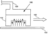
Figure 1A is approaching 110 the end view with heating part 190 that illustrates according to the embodiment of the invention.In exemplary semiconductor wafer processing system 100, be connected to fluid source 120 by connector 130 near 110.Fluid source 120 provides the fluid that uses in the semiconductor wafer process operation.Exemplary fluid can comprise the combination of water, deionized water (DIW), chemical substance (chemistry), chemical substance and DIW and the combination of chemical substance and water.Yet,, clearly can in semiconductor wafer processing system 100, use any fluid that is applicable to semiconductor wafer processing for those skilled in the art.
Though the fluid source 120 shown in Figure 1A have connector 130 with direct fluid near 110, another embodiment can be directly connected to fluid source 120 near 110.After approaching 110 received fluid, fluid flowed in the heating part 190.Heating part 190 is heated to design temperature with fluid.In addition, near 110 by applying heat or waiting for the temperature of controlling fluid, the fluid in heating part 190 reaches design temperature.Fluid flows through when reaching design temperature near one or more outlet on 110 bottom surface.Subsequently, touch the surface of the wafer 150 of locating by wafer maintaining part 140 through the fluid of heating.Wafer maintaining part 140 can support wafer 150 near near 110 bottom surface.
In certain embodiments, can during the semiconductor wafer manufacturing operation, handle substrate (substrate).For example, substrate can take different shapes, the square or the rectangular shape that for example adopt in the flat substrate.Yet,, the circular wafer such as wafer 150 is described in order to simplify.In addition, wafer 150 can be with respect to moving near 110 rotation or straight line.The actual diameter of wafer 150 can change.This example comprises 200mm wafer and 300mm wafer.Yet for those of ordinary skills, clearly, as long as wafer 150 can be placed near near 100 bottom surface, any wafer size and shape all are fine.
Can with offer by first outlet 192 wafer 150 through heating fluid with export the 191 not heating fluids that provide by second and mix mutually.Correspondingly, the 3rd outlet 196 can provide isopropyl alcohol (IPA), and vacuum inlet 194 is from all fluids of surface removal of wafer 150.In certain embodiments, the 3rd outlet 196 can not provide IPA.Therefore, in certain embodiments, vacuum inlet 194 is only removed through the fluid of heating with without the fluid that heats.Any fluid that offers the surface of wafer 150 can have coverage rate (footprint) arbitrarily.For example, the fluid coverage rate can be about two square inches.Yet any fluid coverage rate all is fine, as long as can be by vacuum port 194 with the surface removal of this fluid from wafer 150.
In certain embodiments, wafer 150 can be fixed, and moves with respect to wafer 150 near 110.For example, Figure 1B is another approaching 110 the end view with heating part 190 that illustrates according to the embodiment of the invention.Should can move along direction 160 in the surface of wafer 150 for approaching 110.During moving, provide fluid by being arranged on by heating part 190 heating near a plurality of openings (port) on 110 the bottom surface near head.Certainly, for those of ordinary skills, clearly, as long as approaching 110 does not bump with wafer 150, approaching 110 just can be moved along any direction.
Although one approaching 110 can provide fluid to a surface of wafer 150, Fig. 1 C then is the end view that illustrates according to the semiconductor wafer processing system 100 with two approaching heads of the embodiment of the invention.Can move along the direction that illustrates (for example, direction 160) for approaching 110.Yet near shown in the head, approaching 110 can be different as two.For example, be plotted in the top near 110 heating parts of having described to cover near 110 whole top 190.Alternatively, be plotted in the below near 110 heating parts of having described to cover near the part on 110 top 190.In addition, be plotted in being connected with preheater 170 of below near 110.Preheater 170 can improve the temperature of the fluid that will flow into heating part 190.Then, through the fluid inflow heating part 190 of preheating, finally to be heated to design temperature.Therefore preheater 170 makes fluid can reach higher temperature.In addition, carry out preheating, can control better heating in the short period of time for approaching 110 through the preheating fluid by convection cell.
Fig. 1 D is the end view that is connected to approaching 110 semiconductor wafer processing system 100 of energy source 180 according to having of the embodiment of the invention.And have a plurality of be used to provide through the outlet of heating fluid near different, another embodiment can will offer the surface of wafer 150 through heating fluid by an outlet 192.Heating part 190 is arranged near in certain part of 110.To shown in 1D and the follow-up accompanying drawing, heating part 190 can have arbitrary dimension and shape as Figure 1A.In addition, heating part 190 can surround approaching 110 zone partly or completely.In addition, though heating part 190 is arranged in approaching 110 fully, other embodiment can partly be arranged on heating part 190 (not shown) in approaching 110.Yet,, the size and dimension of heating part 190 can be set by any means in approaching 110 as long as heating part 190 is configured so that and can also the fluid through heating be offered wafer 150 by heating fluid.
Fluid can pass through connector (for example connector 130) and flow in the heating part 190.In addition, one or more connector can be sent to a plurality of fluids in the heating part 190.For example, the fluid that is used for clean operation can flow into connector 130, and connector 130 can be called as first connector 130.Correspondingly, can flow into second connector 132 such as the fluid of the etch chemistries that is used for etching operation, the fluid that is used for the plating operation can flow into the 3rd connector 134.Certainly, for those of ordinary skills, clearly, one or more connector can be used for the fluid of any amount and type.For example DIW can flow in first connector 130, and chemical substance can flow in second connector 132.Therefore as long as heating part 190 is constituted as convection cell and heats, then can fluid be imported heating part 190 by the connector of any amount.
Be connected to energy source 180 for approaching 110.This energy source 180 imports approaching 110 with electric current.Electric conducting material conducts the current in the heating part 190 and heats with convection cell.Other embodiment can not comprise energy source 180.For example, as illustrated in Figures 5 and 6, do not need energy source 180 to come the fluid in the heating part 190 is heated.If utilize energy source 180 to come heating fluid, energy source 180 can produce about 3kW and comes heating fluid so.Yet this value only is exemplary, as long as energy source 180 can produce enough power and come the fluid in the heating part 190 is heated, any value all is fine.
In other exemplary embodiment, the energy source 180 that does not relate to any kind of electricity all is feasible.For example, known laser heats body surface.Therefore, as long as energy source 180 can apply heat to heating part 190, then the energy source 180 of any kind all is feasible.
Embodiment also comprises transducer 185 and controller 188.This transducer 185 is arranged in approaching 110, is used to measure the temperature of the fluid that flows through heating part 190.In addition, transducer 185 can be arranged in the heating part 190 or can be arranged on outside the heating part 190.For those of ordinary skills, clearly, as long as transducer 185 can be measured the temperature of fluid, transducer 185 just can be arranged on any position.In one embodiment, transducer 185 is thermocouples.Yet the transducer 185 of any kind all is fine, as long as it can measure the temperature of fluid.
What be connected with transducer 185 is controller 188.Controller 188 is constituted as to be controlled the temperature of the fluid in the heating part 190.For example, proportion integration differentiation (PID) controller can be controlled the temperature of fluid.Be provided with design temperature (it is for arriving the temperature of fluid of wafer surface) afterwards, this controller 188 can detect poor between the Current Temperatures of the fluid that obtains by the measurement by transducer 185 and the design temperature.Then, controller 188 determines to impose on from energy source 180 magnitude of current of heating part 190.
The software that is connected in the computing system of controller 188 also can Management Controller 188.For example, during operation, this software is set in 60 ℃ with design temperature.Transducer 185 can be measured fluid temperature (F.T.) and determine whether fluid temperature (F.T.) is lower than 60 ℃.This software uses controller 188 to come the detected temperatures difference then and applies electric current as required.If fluid temperature (F.T.) is higher than 60 ℃, this software is not handled so, waits for that fluid reaches design temperature.For those of ordinary skills, the magnitude of current that can apply and the stand-by period that is used for cooling off are programmed into software.In other embodiments, as long as the heating part 190 in approaching 110 increases the temperature of fluids, the method for then any control fluid temperature (F.T.) all is feasible, no matter uses hardware or software.
Fig. 2 is approaching 110 the end view with resistive heating element that illustrates according to the embodiment of the invention.Heating part 190 can be made of resistive heating element.Exemplary resistive heating element can comprise such as carborundum (SiC), molybdenum disilicide (MoSi
2) or the material of other electric conducting material.Exemplary materials such as carborundum can be heated to about more than 100 ℃.Yet resistive heating element can be any material, as long as this material can be heated to and be equal to, or greater than design temperature.
As shown in Figure 2, resistive heating element can comprise a part of approaching 110.For example, near the part approaching 110 bottom surface can be to this fluid heating before the surface that fluid is offered wafer 150.In other embodiments, whole approaching 110 can be made of resistive heating element.Therefore, any The Nomenclature Composition and Structure of Complexes of resistive heating element all is fine, as long as this resistive heating element can heating fluid.
Embodiment described herein near 110 and the surface of wafer 150 between produce meniscus (fluid meniscus) 210.Can make meniscus 210 and semiconductor wafer process operation stride across wafer 150 explicitly and move, with cleaning and drying crystal wafer 150.For example, comprise that the meniscus 210 through heating fluid can be used for etching and plating operation.For those of ordinary skills, clearly, as long as, comprise that the meniscus 210 through heating fluid just can be used for any semiconductor wafer process operation near 110 can heating fluid.
When fluid source 120 provides fluid when heating to heating part 190, transducer 185 is measured the temperature of fluids.The one or many measurement combines with controller 188 and controls the temperature of fluid.Variable from fluid being offered to offering the time quantum of wafer 150 through heating fluid near 110.For example, fluid temperature (F.T.) being brought up to design temperature may be than waiting for that fluid temperature (F.T.) is reduced to the longer time of design temperature consumption.Therefore, as long as will the temperature of fluid reach design temperature before heating fluid offers wafer 150, then amount all is fine any time.
For temperature be from about 40 ℃ to about 95 ℃ meniscus 210, mainly comprise moisture (water-based) chemical substance through heating fluid, as DIW.Yet in other embodiments, other chemical substance also is fine.For example, as submit on June 27th, 2003 be entitled as " Apparatus and Method for Depositing and Planarizing Thin Filmsof Semiconductor Wafers " the 10/607th, in the disclosed plating operating process of No. 611 U.S. Patent applications (being incorporated herein by reference in its entirety), meniscus 210 can offer the surface of wafer 150 through heating fluid with what comprise the plating chemical substance.
After heating part 190 applies electric current, electron transfer (electron transfer) may influence fluid.For example, Fig. 3 is another approaching 110 the end view that illustrates according to the resistive heating element 330 of having of the embodiment of the invention.Should comprise two heating parts of forming by resistive heating element 320 and insulator 330 190 for approaching 110.When resistive heating element 320 applies electric current, insulator 330 prevents that electron transfer is to the fluid that offers wafer 150 surfaces.The example of insulator 320 comprises polytetrafluoroethylene (PTFE) and the sapphire material that is known as Teflon.PTFE can be the coating that covers resistive heating element 320, and sapphire material can be the plating layer with resistive heating element and fluid isolation.Yet as long as insulator 330 can prevent electron transfer to fluid, the insulator of any kind just all is fine.
Shown in the embodiment of Fig. 3, heating part 190 can surround outlet.In addition, though vertical heating part 190 is shown, the horizontal heating part 190 that surrounds the passage of guiding fluid also is fine, as long as the fluid in 190 pairs of passages of heating part heats.Alternative embodiment can be surrounded the outlet of selection, thereby makes and can carry out the selectivity heating by convection cell.
Fig. 4 is the vertical view that illustrates according to approaching 110 the heating part 190 with lead of the embodiment of the invention.This resistive heating element also can comprise bulk resistor (bulk resistor), and for example lead 420.Lead 420 can be a traverse net, perhaps can have inconsistent shape.Regardless of the formation of lead 420, all also lead 420 is insulated to prevent that electron transfer is to fluid.For example, can be such as the insulator 430 of pottery with fluid and lead 420 insulation.When the line 420 that acts as a guide applied electric current, the fluid that flows through heating part 190 was heated to design temperature.When the fluid through heating arrives wafer 150 surperficial, form meniscus 210 (referring to Fig. 2) near 110.Therefore, when wafer during along direction 400 rotation, preceding limb (leading edge) 480 produces the wet zone of wafers 150, and tail prolongs the dried zone that edge (trailing edge) 490 produces wafers 150.Wet zone produces by offering wafer 150 through heating fluid.Correspondingly, combine wafer 150 and produce near 110 motion and to do the zone with will being pumped in 110 through the fluid of heating.
Fig. 5 is the end view that illustrates according to approaching 110 the heating part 190 with circulating fluid of the embodiment of the invention.In the exemplary embodiment, first passage 510 can be directed to fluid the heating part 190 that is arranged in approaching 110.In heating part 190, second channel 520 circulates circulating fluid, thereby prevents that the fluid in the first passage 510 from mixing mutually with the circulating fluid in the second channel 520.The temperature of the fluid that provides from first passage 510 can be provided by heat exchange circulating fluid.Exemplary circulating fluid can be the moisture chemical substance that provides by the pump (not shown).Yet other embodiment can exchange described circulating fluid and new circulating fluid when described circulating fluid loses the ability that applies heat.Therefore, as long as heating part 190 can heating fluid, the method for any introducing and management cycle fluid just all is fine.
In a further exemplary embodiment, for example the resistive heating element of carborundum can combine with the passage that is used for heat exchange.In such embodiments, do not have energy source 180, therefore do not provide electric current to SiC.Carborundum can high heat conduction.Therefore, because second channel is embedded in the good material of conductivity of heat, so at least one second channel 520 can make circulation of fluid to carry out heat exchange.Yet,, can need the network of second channel 520 to carry out heat exchange so if material (for example pottery) has low heat conductivity.
Except not comprising energy source 180, approaching 110 does not comprise electric insulation yet in Fig. 5.Specifically, because circulating fluid provides heat for fluid, so can be from non-existent electric current generation electron transfer.Certainly, if heating part 190 with energy source 180 be used to make the passage of circulation of fluid combined, can comprise insulation near 110 so.
Fig. 6 is the opposite side view that illustrates according to another approaching 110 the heating part 190 with circulating fluid of the embodiment of the invention.Particularly, different with second channel 520, the second channel 620 of this exemplary embodiment has inconsistent shape.In addition, second channel 620 can separate a gap with first passage 510.When fluid entered heating part 190 through first passage 510, the fluid in circulating fluid in the second channel 620 and the first passage 510 carried out heat exchange.Because the gap separates two passages, can be material with high thermal conductivity so surround the material of two passages.
The method of any heating fluid all is fine.For example, Fig. 2 to 4 shows the method for using resistive heating element to heat.Alternatively, Fig. 5 and 6 shows the illustrative methods of using heat exchanger to heat.In addition, the exemplary combination of resistive heating and heat exchange also is fine.Therefore, if can be near 110 heating part 190 heating fluid, the method for any heating fluid all is fine.
In order to be applied to the surface of wafer 150 through the fluid of heating, approaching 110 can be moved with respect to wafer 150.For example, Fig. 7 A is the vertical view near a scan method that illustrates according to the embodiment of the invention.Should can comprise heating part 190 for approaching 110.In addition, can be connected to the parts of handling near 110 near 110.For example, these parts can be fluid can be provided, remove fluid and make approaching 110 arm that move 720.For example, arm 720 can make near 110 and move along radial direction 712.Alternatively, arm 720 can make near head and move along raster scan (raster scan) direction 714.
Alternatively, Fig. 7 B is another vertical view near a scan method that illustrates according to the embodiment of the invention.In one embodiment, can be longer near 110 than the diameter of wafer 150.Therefore, circulating fluid can be offered second channel 754, and fluid to be heated can be offered first passage 752.Therefore, will when offering wafer 150 surperficial, vertically 740 move heating fluid near 110.Certainly, when having when vertical orientated near 110, moving of horizontal direction (not shown) also is fine.In addition, about Fig. 7 A and 7B, as long as approaching 110 can will offer the surface of wafer 150 through heating fluid, the method for then any scanning wafer 150 all is fine.
Fig. 7 C is the vertical view with the zone of using near 110 heating part 190 according to the wafer 150 of the embodiment of the invention.In one embodiment, approaching 110 comprises a plurality of openings that are used to provide and remove fluid.For example, approaching 110 main body can be made of carborundum.Embedding in the carborundum has a plurality of openings, as first opening 762, second opening 764, the 3rd opening 766 and the 4th opening 768.For example, first opening 762 can provide chemical substance, and second opening 764 can provide DIW.The 3rd opening 766 can be vacuum, and the 4th opening can provide IPA.In other embodiments, as long as a plurality of openings can be from providing through heating fluid near 110, then any amount of opening and combination all are fine.
When wafer 150 during, provide fluid through heating to produce wet zone 780 near 110 along direction 700 rotation.Do zone 785 near 110 by producing through the fluid of heating from the area suction of wafer 150.In addition, when wafer 150 rotations, can throw away from the surface of wafer 150 through heating fluid.Therefore, as long as approaching 110 can be moved by moving explicitly of specific scan method and wafer 150, then any generation wet zone 780 all is fine with the method for doing regional 785.
Fig. 8 is used for heating flow chart near the operation of 110 fluid according to the embodiment of the invention.Can in Fig. 1 D to 4, carry out the following illustrative operation before among the disclosed embodiment.In with the exemplary operation of operating 810 beginnings, determine design temperature.Then, in operation 820, fluid source 120 can provide fluid to approaching 110.Arrive after approaching 110 at fluid, in operation 830, can measure fluid temperature (F.T.) near 110 an interior transducer 185.Then, in operation 840, controller 188 can detect the temperature difference between current fluid temperature (F.T.) and the design temperature.In operation 850, controller 188 also can be by applying heat or controlling temperature by waiting for.
For example, in resistive heating means, heating part 190 can comprise the lead 420 that is connected to energy source 180 and such as the material of carborundum.Energy source 180 can apply electric current with the flow through fluid of heating part 190 of heating to heating part 190.Alternatively, have circulating fluid a plurality of passages can with fluid communication heat to be heated.No matter the method that is used for heating fluid how, controller 188 can be regulated fluid temperature (F.T.), mates up to fluid temperature (F.T.) and design temperature.
Then in operation 860, provide through heating fluid by the outlet that is positioned near 110 bottom surface near 110.Be used for a plurality of semiconductor wafer process operations through heating fluid, for example cleaning and etching operation.After this, will be behind the surface removal of wafer 150 through heating fluid, EO.
For those of ordinary skills, all be exemplary in this description and by the operation shown in the accompanying drawing.In addition, can be with any order executable operations so that can the fluid in approaching 110 be heated.For example, transducer 185 can with the fluid temperature of continuous measurement fluid concurrently is provided.Therefore, operating sequence is not limited to particular order.
In addition, embodiment described here is relevant with following patent application.Particularly, the full content of incorporating following related application by application into: 1) submit on December 24th, 2002, exercise question is the 10/330th, No. 843 U.S. Patent application of " Meniscus, Vacuum, IPA Vapor, Drying Manifold "; 2) submit on December 24th, 2002, exercise question is the 10/330th, No. 897 U.S. Patent application of " System forSubstrate Processing with Meni scus, Vacuum, IPA Vapor, DryingManifold "; 3) submit on March 31st, 2003, exercise question is the 10/404th, No. 270 U.S. Patent application of " Vertical Proximity Processor "; 4) submit on March 31st, 2003, exercise question is the 10/404th, No. 692 U.S. Patent application of " Methods andSystems for Processing a Substrate Using a Dynamic Liquid Meniscus "; 5) submit on June 24th, 2003, exercise question is the 10/603rd, No. 427 U.S. Patent application of " Methods and Systems for Processing a Bevel Edge a SubstrateUsing a Dynamic Liquid Meniscus "; 6) submit on June 24th, 2003, exercise question is the 10/606th, No. 022 U.S. Patent application of " System and Method forIntegrating In-Situ Metrology Within a Wafer Process "; 7) submit on June 30th, 2003, exercise question is the 10/611st, No. 140 U.S. Patent application of " Method and Apparatus for Cleaning a Substrate Using MegasonicPower "; And 8) submit on December 18th, 2003, exercise question is the 10/742nd, No. 303 U.S. Patent application of " Proximity Brush Unit Apparatus and Method ".
Though clear for what understand, by details foregoing invention is described,, obviously can realize some variation and modification within the scope of the appended claims.Therefore, should think that described embodiment is illustrative, and not restrictive, and, the invention is not restricted to the details that this paper provides, but can within the scope of claims and equivalent, change.
Claims (21)
1, a kind of method that is used for semiconductor wafer processing may further comprise the steps:
To providing fluid near head;
To heating near the fluid in the head, wherein said approaching head comprises: heating part is constituted as the temperature of control flows through the fluid of this heating part; Be arranged on described near the transducer in the head; Be arranged on the passage in the heating part, described passage is constituted as the guiding fluid and passes through heating part; And the bottom surface, having a plurality of outlets and at least one vacuum inlet, described a plurality of outlets are communicated with passage fluid in being arranged on heating part; And
The surface that will offer semiconductor wafer through the fluid of heating is to be used for the processing of wafers operation, and wherein said a plurality of outlets and at least one vacuum inlet are opened the meniscus that supports between the surface of the bottom surface of described approaching head and described semiconductor wafer.
2, method according to claim 1, wherein said processing of wafers operation is a clean operation.
3, method according to claim 1, wherein said processing of wafers operation is an etching operation.
4, method according to claim 1, wherein said processing of wafers operation is the plating operation.
5, method according to claim 2, the fluid that uses in the wherein said clean operation are one of cleaning chemistry material and deionized water.
6, method according to claim 3, the fluid that uses in the wherein said etching operation is an etch chemistries.
7, method according to claim 1, wherein said to further may further comprise the steps near a step that interior fluid heats:
To controlling near the temperature of the fluid in the head.
8, method according to claim 7, wherein said to further may further comprise the steps near a step that the temperature of interior fluid is controlled:
Temperature near the fluid in the head is monitored; And
The heating of regulating convection cell remains on desired temperature with the temperature with fluid.
9, method according to claim 1 further may further comprise the steps:
The fluid of surface removal from semiconductor wafer through heating.
10, a kind of be used for semiconductor wafer processing near head, comprising:
Heating part is constituted as the temperature of control flows through the fluid of this heating part;
Be arranged on describedly, be used to measure the temperature of fluid of heating part of flowing through near the transducer in the head;
Be arranged on the passage in the heating part, described passage is constituted as the guiding fluid and passes through heating part; And
The bottom surface, have a plurality of outlets and at least one vacuum inlet, described a plurality of outlet is communicated with passage fluid in being arranged on heating part, and described a plurality of outlet and at least one vacuum inlet open to described near head the bottom surface and the surface of described semiconductor wafer between the meniscus that supports.
11, according to claim 10 near head, wherein, described heating part is made up of carborundum, and is connected to energy source.
12, according to claim 10 near head, wherein, described heating part is made up of the insulating material that wherein is scattered with electric conducting material, and described electric conducting material is connected to energy source.
13, according to claim 12 near head, wherein, described insulating material is made up of ceramic material.
14, according to claim 12 near head, wherein, described electric conducting material comprises lead.
15, according to claim 10 near head, wherein, described passage in the described heating part is a first passage, and, described heating part also comprises second channel, wherein said first passage and described second channel are that the material by high thermal conductivity separates, so that circulating fluid in the described second channel and the fluid in the first passage carry out heat exchange.
16, according to claim 10 near head, wherein, transducer is connected to a controller, and this controller is constituted as to be controlled the temperature of the fluid in the heating part.
17, a kind of semiconductor wafer processing system comprises:
Fluid source;
With fluid source flow is communicated with near head, this is near comprising:
Heating part is constituted as the temperature of control flows through the fluid of this heating part,
Be arranged on describedly, be used to measure the temperature of fluid of heating part of flowing through near the transducer in the head,
Be arranged on the passage in the heating part, described passage is constituted as the guiding fluid by heating part, and
The bottom surface, have a plurality of outlets and at least one vacuum inlet, described a plurality of outlet is communicated with passage fluid in being arranged on heating part, and described a plurality of outlet and at least one vacuum inlet open to described near head the bottom surface and the surface of described semiconductor wafer between the meniscus that supports;
Be connected to first parts near head, described first parts are configured to handle near head; And
Be configured to support second parts of described semiconductor wafer, described second parts can be placed semiconductor wafer near the bottom surface near head.
18, semiconductor wafer processing according to claim 17 system, wherein, described heating part is made up of carborundum, and is connected to energy source.
19, semiconductor wafer processing according to claim 17 system, wherein, described heating part is made up of the insulating material that wherein is scattered with electric conducting material, and described electric conducting material is connected to energy source.
20, semiconductor wafer processing according to claim 17 system, wherein, described passage in the described heating part is a first passage, and, described heating part also comprises having second channel, wherein said first passage and described second channel are that the material by high thermal conductivity separates, so that circulating fluid in the described second channel and the fluid in the first passage carry out heat exchange.
21, semiconductor wafer processing according to claim 17 system, wherein, described transducer is connected to a controller, and this controller is constituted as to be controlled the temperature of the fluid in the heating part.
Applications Claiming Priority (2)
| Application Number | Priority Date | Filing Date | Title |
|---|---|---|---|
| US10/816,487 US8062471B2 (en) | 2004-03-31 | 2004-03-31 | Proximity head heating method and apparatus |
| US10/816,487 | 2004-03-31 |
Publications (2)
| Publication Number | Publication Date |
|---|---|
| CN1722372A CN1722372A (en) | 2006-01-18 |
| CN100505170C true CN100505170C (en) | 2009-06-24 |
Family
ID=34887763
Family Applications (1)
| Application Number | Title | Priority Date | Filing Date |
|---|---|---|---|
| CNB200510063774XA Expired - Fee Related CN100505170C (en) | 2004-03-31 | 2005-03-31 | Proximity head heating method and apparatus |
Country Status (10)
| Country | Link |
|---|---|
| US (2) | US8062471B2 (en) |
| EP (1) | EP1583135B1 (en) |
| JP (1) | JP4621052B2 (en) |
| KR (1) | KR101209537B1 (en) |
| CN (1) | CN100505170C (en) |
| AT (1) | ATE384334T1 (en) |
| DE (1) | DE602005004321T2 (en) |
| MY (1) | MY138431A (en) |
| SG (1) | SG115790A1 (en) |
| TW (1) | TWI289322B (en) |
Cited By (1)
| Publication number | Priority date | Publication date | Assignee | Title |
|---|---|---|---|---|
| CN106098586A (en) * | 2015-04-27 | 2016-11-09 | 台湾积体电路制造股份有限公司 | For the method that etching layer is etched and crystal round etching device |
Families Citing this family (34)
| Publication number | Priority date | Publication date | Assignee | Title |
|---|---|---|---|---|
| US7329321B2 (en) * | 2002-09-30 | 2008-02-12 | Lam Research Corporation | Enhanced wafer cleaning method |
| US7632376B1 (en) * | 2002-09-30 | 2009-12-15 | Lam Research Corporation | Method and apparatus for atomic layer deposition (ALD) in a proximity system |
| US8062471B2 (en) * | 2004-03-31 | 2011-11-22 | Lam Research Corporation | Proximity head heating method and apparatus |
| US9117860B2 (en) * | 2006-08-30 | 2015-08-25 | Lam Research Corporation | Controlled ambient system for interface engineering |
| KR101453115B1 (en) * | 2006-09-29 | 2014-10-27 | 램 리써치 코포레이션 | Reduction of entrance and exit marks left by a substrate-processing meniscus |
| US7946303B2 (en) * | 2006-09-29 | 2011-05-24 | Lam Research Corporation | Carrier for reducing entrance and/or exit marks left by a substrate-processing meniscus |
| ES2394167T3 (en) * | 2006-10-16 | 2013-01-23 | Materials And Technologies Corporation | Wet processing apparatus using a fluid meniscus |
| US8309470B2 (en) * | 2006-12-18 | 2012-11-13 | Lam Research Corporation | In-situ reclaim of volatile components |
| US7897213B2 (en) * | 2007-02-08 | 2011-03-01 | Lam Research Corporation | Methods for contained chemical surface treatment |
| DE102007026635B4 (en) * | 2007-06-06 | 2010-07-29 | Atotech Deutschland Gmbh | Apparatus for wet-chemical treatment of goods, use of a flow organ, method for installing a flow organ in the device and method for producing a wet-chemical treated goods |
| KR100908017B1 (en) * | 2007-11-13 | 2009-07-15 | 조선대학교산학협력단 | Polishing Pad Conditioning Device |
| CN101971295B (en) * | 2007-12-20 | 2012-05-30 | 朗姆研究公司 | Methods of configuring a proximity head that provides uniform fluid flow relative to a wafer |
| US8317934B2 (en) * | 2009-05-13 | 2012-11-27 | Lam Research Corporation | Multi-stage substrate cleaning method and apparatus |
| US20110139183A1 (en) * | 2009-12-11 | 2011-06-16 | Katrina Mikhaylichenko | System and method of preventing pattern collapse using low surface tension fluid |
| EP2383771B1 (en) * | 2010-04-29 | 2020-04-22 | EV Group GmbH | Method and device for loosening a polymer coating from a surface of a substrate |
| JP5031066B2 (en) * | 2010-05-26 | 2012-09-19 | 兵庫県 | Cluster beam generating apparatus, substrate processing apparatus, cluster beam generating method, and substrate processing method |
| FI124113B (en) * | 2010-08-30 | 2014-03-31 | Beneq Oy | Apparatus and method for working the surface of a substrate |
| KR20120034948A (en) * | 2010-10-04 | 2012-04-13 | 삼성전자주식회사 | Apparatus for drying a substrate and method for performing the same using thereof |
| JP2012222254A (en) * | 2011-04-12 | 2012-11-12 | Tokyo Electron Ltd | Substrate cleaning-nozzle, substrate cleaning device, and substrate cleaning method |
| JP5894854B2 (en) * | 2012-05-11 | 2016-03-30 | 株式会社日立ハイテクノロジーズ | Inspection device |
| US9870933B2 (en) * | 2013-02-08 | 2018-01-16 | Lam Research Ag | Process and apparatus for treating surfaces of wafer-shaped articles |
| US20140352735A1 (en) * | 2013-05-29 | 2014-12-04 | Beijing Sevenstar Electronics Co. Ltd. | Zero lag dispense apparatus |
| DE102013010934A1 (en) * | 2013-06-29 | 2015-01-15 | Feinmetall Gmbh | Test device for electrical testing of an electrical device under test |
| JP2015115492A (en) * | 2013-12-12 | 2015-06-22 | 株式会社Screenホールディングス | Substrate processing apparatus |
| US9966282B2 (en) * | 2014-09-30 | 2018-05-08 | Shibaura Mechatronics Corporation | Substrate processing apparatus and substrate processing method |
| JP6558845B2 (en) * | 2014-10-10 | 2019-08-14 | 株式会社ホロン | Foreign matter removing apparatus for foreign matter and method for removing foreign matter |
| JP6467260B2 (en) * | 2015-03-24 | 2019-02-06 | 株式会社Screenホールディングス | Substrate processing method and substrate processing apparatus |
| JP6505495B2 (en) * | 2015-04-28 | 2019-04-24 | 株式会社ディスコ | Processing device |
| RU2599314C1 (en) * | 2015-04-29 | 2016-10-10 | Андрей Николаевич Алексеев | Method for maintaining temperature of heated "live" electrolyte baths |
| RU2632727C2 (en) * | 2016-02-26 | 2017-10-09 | Андрей Николаевич Алексеев | Method of maintaining level of electrolyte-heated bath operated under current |
| JP6709010B2 (en) * | 2019-04-16 | 2020-06-10 | 株式会社ホロン | Foreign object removing device for cleaning object and foreign object removing method |
| CN113441449B (en) * | 2020-03-27 | 2022-12-09 | 先丰通讯股份有限公司 | Spray plate detection system and detection method thereof |
| CN111604307B (en) * | 2020-05-24 | 2022-07-05 | 国网黑龙江省电力有限公司齐齐哈尔供电公司 | Electric power engineering insulator cleaning system and cleaning method |
| RU2761305C1 (en) * | 2020-09-29 | 2021-12-07 | Андрей Николаевич Алексеев | Method for controlling the operations of flushing of parts in a galvanic line made in a single-level layout |
Family Cites Families (110)
| Publication number | Priority date | Publication date | Assignee | Title |
|---|---|---|---|---|
| US3953265A (en) * | 1975-04-28 | 1976-04-27 | International Business Machines Corporation | Meniscus-contained method of handling fluids in the manufacture of semiconductor wafers |
| US4086870A (en) * | 1977-06-30 | 1978-05-02 | International Business Machines Corporation | Novel resist spinning head |
| US4367123A (en) * | 1980-07-09 | 1983-01-04 | Olin Corporation | Precision spot plating process and apparatus |
| JPS5852034B2 (en) | 1981-08-26 | 1983-11-19 | 株式会社ソニツクス | Partial plating method and device |
| US4444492A (en) * | 1982-05-15 | 1984-04-24 | General Signal Corporation | Apparatus for projecting a series of images onto dies of a semiconductor wafer |
| US4838289A (en) * | 1982-08-03 | 1989-06-13 | Texas Instruments Incorporated | Apparatus and method for edge cleaning |
| JPS62150828A (en) | 1985-12-25 | 1987-07-04 | Mitsubishi Electric Corp | Wafer drying apparatus |
| JPH0712035B2 (en) | 1989-04-20 | 1995-02-08 | 三菱電機株式会社 | Jet type liquid treatment device |
| JPH02309638A (en) | 1989-05-24 | 1990-12-25 | Fujitsu Ltd | Wafer etching device |
| JPH0628223Y2 (en) * | 1989-06-14 | 1994-08-03 | 大日本スクリーン製造株式会社 | Spin coating device |
| US5271774A (en) * | 1990-03-01 | 1993-12-21 | U.S. Philips Corporation | Method for removing in a centrifuge a liquid from a surface of a substrate |
| US5102494A (en) * | 1990-07-13 | 1992-04-07 | Mobil Solar Energy Corporation | Wet-tip die for EFG cyrstal growth apparatus |
| US5294257A (en) * | 1991-10-28 | 1994-03-15 | International Business Machines Corporation | Edge masking spin tool |
| US5343234A (en) * | 1991-11-15 | 1994-08-30 | Kuehnle Manfred R | Digital color proofing system and method for offset and gravure printing |
| JP2877216B2 (en) * | 1992-10-02 | 1999-03-31 | 東京エレクトロン株式会社 | Cleaning equipment |
| US5339842A (en) * | 1992-12-18 | 1994-08-23 | Specialty Coating Systems, Inc. | Methods and apparatus for cleaning objects |
| US5472502A (en) * | 1993-08-30 | 1995-12-05 | Semiconductor Systems, Inc. | Apparatus and method for spin coating wafers and the like |
| US5807522A (en) * | 1994-06-17 | 1998-09-15 | The Board Of Trustees Of The Leland Stanford Junior University | Methods for fabricating microarrays of biological samples |
| ATE184185T1 (en) * | 1994-06-30 | 1999-09-15 | Procter & Gamble | LIQUID CONDUCTIVE FABRIC WITH SURFACE ENERGY GRADIENTS |
| US5705223A (en) * | 1994-07-26 | 1998-01-06 | International Business Machine Corp. | Method and apparatus for coating a semiconductor wafer |
| JP3247270B2 (en) * | 1994-08-25 | 2002-01-15 | 東京エレクトロン株式会社 | Processing apparatus and dry cleaning method |
| US5558111A (en) * | 1995-02-02 | 1996-09-24 | International Business Machines Corporation | Apparatus and method for carrier backing film reconditioning |
| US5601655A (en) * | 1995-02-14 | 1997-02-11 | Bok; Hendrik F. | Method of cleaning substrates |
| JP3327726B2 (en) * | 1995-04-03 | 2002-09-24 | キヤノン株式会社 | Ink jet recording device |
| JPH08277486A (en) | 1995-04-04 | 1996-10-22 | Dainippon Printing Co Ltd | Plating device for lead frame |
| US5618594A (en) * | 1995-04-13 | 1997-04-08 | Cvd, Incorporated | Composite thermocouple protection tubes |
| TW386235B (en) * | 1995-05-23 | 2000-04-01 | Tokyo Electron Ltd | Method for spin rinsing |
| US5660642A (en) * | 1995-05-26 | 1997-08-26 | The Regents Of The University Of California | Moving zone Marangoni drying of wet objects using naturally evaporated solvent vapor |
| EP0764837A1 (en) * | 1995-09-25 | 1997-03-26 | Isuzu Ceramics Research Institute Co., Ltd. | Thermocouple structure |
| US5975098A (en) * | 1995-12-21 | 1999-11-02 | Dainippon Screen Mfg. Co., Ltd. | Apparatus for and method of cleaning substrate |
| DE19622015A1 (en) * | 1996-05-31 | 1997-12-04 | Siemens Ag | Process for etching destruction zones on a semiconductor substrate edge and etching system |
| US5985031A (en) * | 1996-06-21 | 1999-11-16 | Micron Technology, Inc. | Spin coating spindle and chuck assembly |
| US6090210A (en) * | 1996-07-24 | 2000-07-18 | Applied Materials, Inc. | Multi-zone gas flow control in a process chamber |
| TW357406B (en) * | 1996-10-07 | 1999-05-01 | Tokyo Electron Ltd | Method and apparatus for cleaning and drying a substrate |
| US5830334A (en) * | 1996-11-07 | 1998-11-03 | Kobayashi; Hideyuki | Nozzle for fast plating with plating solution jetting and suctioning functions |
| JPH10163138A (en) * | 1996-11-29 | 1998-06-19 | Fujitsu Ltd | Manufacture of semiconductor device and polisher |
| JPH1133506A (en) * | 1997-07-24 | 1999-02-09 | Tadahiro Omi | Fluid treatment device and cleaning treatment system |
| JP2951903B2 (en) | 1997-01-09 | 1999-09-20 | 株式会社日立製作所 | Processing equipment |
| JPH10232498A (en) * | 1997-02-19 | 1998-09-02 | Nec Kyushu Ltd | Developing device |
| JP2983494B2 (en) * | 1997-05-20 | 1999-11-29 | 株式会社カイジョー | Substrate drying method |
| JPH1131672A (en) | 1997-07-10 | 1999-02-02 | Hitachi Ltd | Substrate-processing method and substrate processor |
| US6103636A (en) * | 1997-08-20 | 2000-08-15 | Micron Technology, Inc. | Method and apparatus for selective removal of material from wafer alignment marks |
| DE69828592T8 (en) | 1997-09-24 | 2006-06-08 | Interuniversitair Micro-Elektronica Centrum Vzw | METHOD FOR REMOVING A LIQUID FROM A SURFACE OF A SUBSTRATE |
| JP4616948B2 (en) | 1997-09-24 | 2011-01-19 | アイメック | Method and apparatus for removing liquid from the surface of a rotating substrate |
| US6398975B1 (en) * | 1997-09-24 | 2002-06-04 | Interuniversitair Microelektronica Centrum (Imec) | Method and apparatus for localized liquid treatment of the surface of a substrate |
| US6491764B2 (en) * | 1997-09-24 | 2002-12-10 | Interuniversitair Microelektronics Centrum (Imec) | Method and apparatus for removing a liquid from a surface of a rotating substrate |
| EP0905746A1 (en) | 1997-09-24 | 1999-03-31 | Interuniversitair Micro-Elektronica Centrum Vzw | Method of removing a liquid from a surface of a rotating substrate |
| EP1055020A2 (en) * | 1998-02-12 | 2000-11-29 | ACM Research, Inc. | Plating apparatus and method |
| AU2747999A (en) | 1998-03-26 | 1999-10-18 | Nikon Corporation | Projection exposure method and system |
| US6108932A (en) * | 1998-05-05 | 2000-08-29 | Steag Microtech Gmbh | Method and apparatus for thermocapillary drying |
| JPH11350169A (en) | 1998-06-10 | 1999-12-21 | Chemitoronics Co | Wet etching apparatus and wet etching method |
| US6132586A (en) * | 1998-06-11 | 2000-10-17 | Integrated Process Equipment Corporation | Method and apparatus for non-contact metal plating of semiconductor wafers using a bipolar electrode assembly |
| US6689323B2 (en) * | 1998-10-30 | 2004-02-10 | Agilent Technologies | Method and apparatus for liquid transfer |
| US6092937A (en) * | 1999-01-08 | 2000-07-25 | Fastar, Ltd. | Linear developer |
| US6169244B1 (en) * | 1999-05-21 | 2001-01-02 | Moore Epitaxial, Inc. | Thermocouple sheath cover |
| JP3653198B2 (en) * | 1999-07-16 | 2005-05-25 | アルプス電気株式会社 | Nozzle for drying, drying apparatus and cleaning apparatus using the same |
| US20020121290A1 (en) * | 1999-08-25 | 2002-09-05 | Applied Materials, Inc. | Method and apparatus for cleaning/drying hydrophobic wafers |
| JP3635217B2 (en) * | 1999-10-05 | 2005-04-06 | 東京エレクトロン株式会社 | Liquid processing apparatus and method |
| WO2001027357A1 (en) * | 1999-10-12 | 2001-04-19 | Semitool, Inc. | Method and apparatus for executing plural processes on a microelectronic workpiece at a single processing station |
| US6341998B1 (en) * | 1999-11-04 | 2002-01-29 | Vlsi Technology, Inc. | Integrated circuit (IC) plating deposition system and method |
| US6214513B1 (en) * | 1999-11-24 | 2001-04-10 | Xerox Corporation | Slot coating under an electric field |
| US6433541B1 (en) * | 1999-12-23 | 2002-08-13 | Kla-Tencor Corporation | In-situ metalization monitoring using eddy current measurements during the process for removing the film |
| JP2001220688A (en) | 2000-02-09 | 2001-08-14 | Matsushita Electric Ind Co Ltd | Thin film deposition system and thin film deposition method |
| US20030091754A1 (en) * | 2000-02-11 | 2003-05-15 | Thami Chihani | Method for treating cellulosic fibres |
| US6474786B2 (en) * | 2000-02-24 | 2002-11-05 | The Board Of Trustees Of The Leland Stanford Junior University | Micromachined two-dimensional array droplet ejectors |
| US6495005B1 (en) * | 2000-05-01 | 2002-12-17 | International Business Machines Corporation | Electroplating apparatus |
| JP2004500975A (en) * | 2000-05-16 | 2004-01-15 | リージェンツ オブ ザ ユニバーシティ オブ ミネソタ | High throughput particle generator and particle generation method using multiple nozzle spray operations |
| JP4567148B2 (en) * | 2000-06-23 | 2010-10-20 | 東京エレクトロン株式会社 | Thin film forming equipment |
| EP1295314A2 (en) | 2000-06-26 | 2003-03-26 | Applied Materials, Inc. | Method and apparatus for wafer cleaning |
| US6488040B1 (en) * | 2000-06-30 | 2002-12-03 | Lam Research Corporation | Capillary proximity heads for single wafer cleaning and drying |
| US7000622B2 (en) * | 2002-09-30 | 2006-02-21 | Lam Research Corporation | Methods and systems for processing a bevel edge of a substrate using a dynamic liquid meniscus |
| US7234477B2 (en) * | 2000-06-30 | 2007-06-26 | Lam Research Corporation | Method and apparatus for drying semiconductor wafer surfaces using a plurality of inlets and outlets held in close proximity to the wafer surfaces |
| US6530823B1 (en) * | 2000-08-10 | 2003-03-11 | Nanoclean Technologies Inc | Methods for cleaning surfaces substantially free of contaminants |
| JP2002075947A (en) * | 2000-08-30 | 2002-03-15 | Alps Electric Co Ltd | Wet processor |
| US6555017B1 (en) * | 2000-10-13 | 2003-04-29 | The Regents Of The University Of Caliofornia | Surface contouring by controlled application of processing fluid using Marangoni effect |
| US6550988B2 (en) * | 2000-10-30 | 2003-04-22 | Dainippon Screen Mfg., Co., Ltd. | Substrate processing apparatus |
| US6531206B2 (en) * | 2001-02-07 | 2003-03-11 | 3M Innovative Properties Company | Microstructured surface film assembly for liquid acquisition and transport |
| KR20090104115A (en) | 2001-06-12 | 2009-10-05 | 아크리온 테크놀로지즈 인코포레이티드 | Megasonic Cleaner and Dryer System |
| TW554069B (en) | 2001-08-10 | 2003-09-21 | Ebara Corp | Plating device and method |
| JP4785306B2 (en) * | 2001-09-17 | 2011-10-05 | キヤノン株式会社 | Ink jet recording apparatus and ink temperature control method in the apparatus |
| JP2003115474A (en) * | 2001-10-03 | 2003-04-18 | Ebara Corp | Substrate processor and processing method |
| JP4003441B2 (en) | 2001-11-08 | 2007-11-07 | セイコーエプソン株式会社 | Surface treatment apparatus and surface treatment method |
| US6799584B2 (en) * | 2001-11-09 | 2004-10-05 | Applied Materials, Inc. | Condensation-based enhancement of particle removal by suction |
| US6845778B2 (en) * | 2002-03-29 | 2005-01-25 | Lam Research Corporation | In-situ local heating using megasonic transducer resonator |
| TWI274393B (en) | 2002-04-08 | 2007-02-21 | Acm Res Inc | Electropolishing and/or electroplating apparatus and methods |
| US7069937B2 (en) * | 2002-09-30 | 2006-07-04 | Lam Research Corporation | Vertical proximity processor |
| US7093375B2 (en) * | 2002-09-30 | 2006-08-22 | Lam Research Corporation | Apparatus and method for utilizing a meniscus in substrate processing |
| US6988326B2 (en) * | 2002-09-30 | 2006-01-24 | Lam Research Corporation | Phobic barrier meniscus separation and containment |
| US7252097B2 (en) * | 2002-09-30 | 2007-08-07 | Lam Research Corporation | System and method for integrating in-situ metrology within a wafer process |
| CN100350552C (en) | 2002-09-30 | 2007-11-21 | 拉姆研究公司 | System for substrate processing with meniscus, vacuum, IPA vapor, drying manifold |
| US7383843B2 (en) * | 2002-09-30 | 2008-06-10 | Lam Research Corporation | Method and apparatus for processing wafer surfaces using thin, high velocity fluid layer |
| US7293571B2 (en) * | 2002-09-30 | 2007-11-13 | Lam Research Corporation | Substrate proximity processing housing and insert for generating a fluid meniscus |
| US7513262B2 (en) * | 2002-09-30 | 2009-04-07 | Lam Research Corporation | Substrate meniscus interface and methods for operation |
| US7389783B2 (en) * | 2002-09-30 | 2008-06-24 | Lam Research Corporation | Proximity meniscus manifold |
| US7153400B2 (en) * | 2002-09-30 | 2006-12-26 | Lam Research Corporation | Apparatus and method for depositing and planarizing thin films of semiconductor wafers |
| US6954993B1 (en) * | 2002-09-30 | 2005-10-18 | Lam Research Corporation | Concentric proximity processing head |
| US7329321B2 (en) * | 2002-09-30 | 2008-02-12 | Lam Research Corporation | Enhanced wafer cleaning method |
| US7240679B2 (en) * | 2002-09-30 | 2007-07-10 | Lam Research Corporation | System for substrate processing with meniscus, vacuum, IPA vapor, drying manifold |
| US6988327B2 (en) * | 2002-09-30 | 2006-01-24 | Lam Research Corporation | Methods and systems for processing a substrate using a dynamic liquid meniscus |
| US7614411B2 (en) * | 2002-09-30 | 2009-11-10 | Lam Research Corporation | Controls of ambient environment during wafer drying using proximity head |
| SG121822A1 (en) * | 2002-11-12 | 2006-05-26 | Asml Netherlands Bv | Lithographic apparatus and device manufacturing method |
| EP1489461A1 (en) | 2003-06-11 | 2004-12-22 | ASML Netherlands B.V. | Lithographic apparatus and device manufacturing method |
| US6867844B2 (en) | 2003-06-19 | 2005-03-15 | Asml Holding N.V. | Immersion photolithography system and method using microchannel nozzles |
| US7231682B1 (en) * | 2003-08-28 | 2007-06-19 | Lam Research Corporation | Method and apparatus for simultaneously cleaning the front side and back side of a wafer |
| US7353560B2 (en) * | 2003-12-18 | 2008-04-08 | Lam Research Corporation | Proximity brush unit apparatus and method |
| US7645341B2 (en) * | 2003-12-23 | 2010-01-12 | Lam Research Corporation | Showerhead electrode assembly for plasma processing apparatuses |
| US8062471B2 (en) * | 2004-03-31 | 2011-11-22 | Lam Research Corporation | Proximity head heating method and apparatus |
| US7003899B1 (en) * | 2004-09-30 | 2006-02-28 | Lam Research Corporation | System and method for modulating flow through multiple ports in a proximity head |
| US20080260963A1 (en) * | 2007-04-17 | 2008-10-23 | Hyungsuk Alexander Yoon | Apparatus and method for pre and post treatment of atomic layer deposition |
| US8309470B2 (en) * | 2006-12-18 | 2012-11-13 | Lam Research Corporation | In-situ reclaim of volatile components |
-
2004
- 2004-03-31 US US10/816,487 patent/US8062471B2/en not_active Expired - Fee Related
-
2005
- 2005-03-18 SG SG200501830A patent/SG115790A1/en unknown
- 2005-03-21 EP EP05251719A patent/EP1583135B1/en not_active Not-in-force
- 2005-03-21 DE DE602005004321T patent/DE602005004321T2/en active Active
- 2005-03-21 AT AT05251719T patent/ATE384334T1/en not_active IP Right Cessation
- 2005-03-29 MY MYPI20051369A patent/MY138431A/en unknown
- 2005-03-30 KR KR1020050026675A patent/KR101209537B1/en not_active IP Right Cessation
- 2005-03-30 JP JP2005096581A patent/JP4621052B2/en not_active Expired - Fee Related
- 2005-03-30 TW TW094110018A patent/TWI289322B/en not_active IP Right Cessation
- 2005-03-31 CN CNB200510063774XA patent/CN100505170C/en not_active Expired - Fee Related
-
2010
- 2010-09-20 US US12/886,278 patent/US8102014B2/en not_active Expired - Fee Related
Cited By (3)
| Publication number | Priority date | Publication date | Assignee | Title |
|---|---|---|---|---|
| CN106098586A (en) * | 2015-04-27 | 2016-11-09 | 台湾积体电路制造股份有限公司 | For the method that etching layer is etched and crystal round etching device |
| US10283384B2 (en) | 2015-04-27 | 2019-05-07 | Taiwan Semiconductor Manufacturing Co., Ltd. | Method for etching etch layer and wafer etching apparatus |
| US11784065B2 (en) | 2015-04-27 | 2023-10-10 | Taiwan Semiconductor Manufacturing Co., Ltd. | Method for etching etch layer |
Also Published As
| Publication number | Publication date |
|---|---|
| US20110008916A1 (en) | 2011-01-13 |
| DE602005004321D1 (en) | 2008-03-06 |
| EP1583135A1 (en) | 2005-10-05 |
| US20050221621A1 (en) | 2005-10-06 |
| CN1722372A (en) | 2006-01-18 |
| US8062471B2 (en) | 2011-11-22 |
| ATE384334T1 (en) | 2008-02-15 |
| MY138431A (en) | 2009-06-30 |
| EP1583135B1 (en) | 2008-01-16 |
| TW200601399A (en) | 2006-01-01 |
| US8102014B2 (en) | 2012-01-24 |
| KR20060045033A (en) | 2006-05-16 |
| SG115790A1 (en) | 2005-10-28 |
| TWI289322B (en) | 2007-11-01 |
| DE602005004321T2 (en) | 2008-12-24 |
| JP4621052B2 (en) | 2011-01-26 |
| JP2005328038A (en) | 2005-11-24 |
| KR101209537B1 (en) | 2012-12-07 |
Similar Documents
| Publication | Publication Date | Title |
|---|---|---|
| CN100505170C (en) | Proximity head heating method and apparatus | |
| CN103201826B (en) | The hot plate with planar heater zone for semiconductor processes | |
| KR101958018B1 (en) | Electrostatic chuck with advanced rf and temperature uniformity | |
| JP4772779B2 (en) | Temperature control method and temperature control apparatus | |
| KR101229694B1 (en) | Fluid heater, manufacturing method thereof, substrate processing device equipped with a fluid heater, and substrate processing method | |
| JP5183058B2 (en) | Substrate processing with rapid temperature gradient control | |
| US6845778B2 (en) | In-situ local heating using megasonic transducer resonator | |
| US11532492B2 (en) | Substrate processing apparatus and substrate processing method | |
| CN101154612B (en) | Temperature controlled substrate holder having erosion resistant insulating layer for a substrate processing system | |
| JP2013534716A (en) | Apparatus and method for temperature control of semiconductor substrate support | |
| CN106057708A (en) | Heating plate with diode planar heater zones for semiconductor processing | |
| JP2021525454A (en) | Extremely uniform heating substrate support assembly | |
| EP1676295A2 (en) | Apparatus to improve wafer temperature uniformity for face-up wet processing | |
| JP6639657B2 (en) | Pressurized chamber with small thermal mass | |
| CN104752136A (en) | Plasma processing device and electrostatic chuck thereof | |
| KR100961861B1 (en) | Susceptor unit, apparatus for manufacturing semiconductor having the susceptor and dry etch method for silicon oxide using the apparatus | |
| KR101296412B1 (en) | Heat treatment apparatus | |
| KR20210018517A (en) | Semiconductor processing units for high RF power processes | |
| JP2018163976A (en) | Substrate processing apparatus and substrate processing method | |
| CN114672789A (en) | Vapor deposition equipment and wafer heating platform deck and heating method thereof | |
| KR101214954B1 (en) | A process gas for heating device supplied to process chamber | |
| CN111383885A (en) | Substrate mounting table capable of improving temperature control precision and plasma processing equipment | |
| US20070215173A1 (en) | Heated single wafer megasonic processing plate |
Legal Events
| Date | Code | Title | Description |
|---|---|---|---|
| C06 | Publication | ||
| PB01 | Publication | ||
| C10 | Entry into substantive examination | ||
| SE01 | Entry into force of request for substantive examination | ||
| C14 | Grant of patent or utility model | ||
| GR01 | Patent grant | ||
| CF01 | Termination of patent right due to non-payment of annual fee | ||
| CF01 | Termination of patent right due to non-payment of annual fee |
Granted publication date: 20090624 Termination date: 20160331 |