CN100521876C - Method for processing a thin film substrate - Google Patents
Method for processing a thin film substrate Download PDFInfo
- Publication number
- CN100521876C CN100521876C CNB2004800116430A CN200480011643A CN100521876C CN 100521876 C CN100521876 C CN 100521876C CN B2004800116430 A CNB2004800116430 A CN B2004800116430A CN 200480011643 A CN200480011643 A CN 200480011643A CN 100521876 C CN100521876 C CN 100521876C
- Authority
- CN
- China
- Prior art keywords
- substrate
- film
- hole
- during
- path
- Prior art date
- Legal status (The legal status is an assumption and is not a legal conclusion. Google has not performed a legal analysis and makes no representation as to the accuracy of the status listed.)
- Active
Links
Images


Classifications
-
- H—ELECTRICITY
- H05—ELECTRIC TECHNIQUES NOT OTHERWISE PROVIDED FOR
- H05K—PRINTED CIRCUITS; CASINGS OR CONSTRUCTIONAL DETAILS OF ELECTRIC APPARATUS; MANUFACTURE OF ASSEMBLAGES OF ELECTRICAL COMPONENTS
- H05K1/00—Printed circuits
- H05K1/02—Details
- H05K1/11—Printed elements for providing electric connections to or between printed circuits
-
- H—ELECTRICITY
- H05—ELECTRIC TECHNIQUES NOT OTHERWISE PROVIDED FOR
- H05K—PRINTED CIRCUITS; CASINGS OR CONSTRUCTIONAL DETAILS OF ELECTRIC APPARATUS; MANUFACTURE OF ASSEMBLAGES OF ELECTRICAL COMPONENTS
- H05K3/00—Apparatus or processes for manufacturing printed circuits
- H05K3/0011—Working of insulating substrates or insulating layers
- H05K3/0017—Etching of the substrate by chemical or physical means
- H05K3/0041—Etching of the substrate by chemical or physical means by plasma etching
-
- H—ELECTRICITY
- H05—ELECTRIC TECHNIQUES NOT OTHERWISE PROVIDED FOR
- H05K—PRINTED CIRCUITS; CASINGS OR CONSTRUCTIONAL DETAILS OF ELECTRIC APPARATUS; MANUFACTURE OF ASSEMBLAGES OF ELECTRICAL COMPONENTS
- H05K1/00—Printed circuits
- H05K1/02—Details
- H05K1/11—Printed elements for providing electric connections to or between printed circuits
- H05K1/115—Via connections; Lands around holes or via connections
-
- H—ELECTRICITY
- H05—ELECTRIC TECHNIQUES NOT OTHERWISE PROVIDED FOR
- H05K—PRINTED CIRCUITS; CASINGS OR CONSTRUCTIONAL DETAILS OF ELECTRIC APPARATUS; MANUFACTURE OF ASSEMBLAGES OF ELECTRICAL COMPONENTS
- H05K3/00—Apparatus or processes for manufacturing printed circuits
- H05K3/40—Forming printed elements for providing electric connections to or between printed circuits
-
- B—PERFORMING OPERATIONS; TRANSPORTING
- B82—NANOTECHNOLOGY
- B82Y—SPECIFIC USES OR APPLICATIONS OF NANOSTRUCTURES; MEASUREMENT OR ANALYSIS OF NANOSTRUCTURES; MANUFACTURE OR TREATMENT OF NANOSTRUCTURES
- B82Y30/00—Nanotechnology for materials or surface science, e.g. nanocomposites
-
- G—PHYSICS
- G01—MEASURING; TESTING
- G01K—MEASURING TEMPERATURE; MEASURING QUANTITY OF HEAT; THERMALLY-SENSITIVE ELEMENTS NOT OTHERWISE PROVIDED FOR
- G01K2211/00—Thermometers based on nanotechnology
-
- H—ELECTRICITY
- H01—ELECTRIC ELEMENTS
- H01L—SEMICONDUCTOR DEVICES NOT COVERED BY CLASS H10
- H01L2924/00—Indexing scheme for arrangements or methods for connecting or disconnecting semiconductor or solid-state bodies as covered by H01L24/00
- H01L2924/0001—Technical content checked by a classifier
- H01L2924/0002—Not covered by any one of groups H01L24/00, H01L24/00 and H01L2224/00
-
- H—ELECTRICITY
- H05—ELECTRIC TECHNIQUES NOT OTHERWISE PROVIDED FOR
- H05K—PRINTED CIRCUITS; CASINGS OR CONSTRUCTIONAL DETAILS OF ELECTRIC APPARATUS; MANUFACTURE OF ASSEMBLAGES OF ELECTRICAL COMPONENTS
- H05K2201/00—Indexing scheme relating to printed circuits covered by H05K1/00
- H05K2201/09—Shape and layout
- H05K2201/09209—Shape and layout details of conductors
- H05K2201/095—Conductive through-holes or vias
- H05K2201/09609—Via grid, i.e. two-dimensional array of vias or holes in a single plane
-
- H—ELECTRICITY
- H05—ELECTRIC TECHNIQUES NOT OTHERWISE PROVIDED FOR
- H05K—PRINTED CIRCUITS; CASINGS OR CONSTRUCTIONAL DETAILS OF ELECTRIC APPARATUS; MANUFACTURE OF ASSEMBLAGES OF ELECTRICAL COMPONENTS
- H05K2201/00—Indexing scheme relating to printed circuits covered by H05K1/00
- H05K2201/09—Shape and layout
- H05K2201/09209—Shape and layout details of conductors
- H05K2201/09654—Shape and layout details of conductors covering at least two types of conductors provided for in H05K2201/09218 - H05K2201/095
- H05K2201/0979—Redundant conductors or connections, i.e. more than one current path between two points
-
- H—ELECTRICITY
- H05—ELECTRIC TECHNIQUES NOT OTHERWISE PROVIDED FOR
- H05K—PRINTED CIRCUITS; CASINGS OR CONSTRUCTIONAL DETAILS OF ELECTRIC APPARATUS; MANUFACTURE OF ASSEMBLAGES OF ELECTRICAL COMPONENTS
- H05K2203/00—Indexing scheme relating to apparatus or processes for manufacturing printed circuits covered by H05K3/00
- H05K2203/09—Treatments involving charged particles
- H05K2203/092—Particle beam, e.g. using an electron beam or an ion beam
-
- H—ELECTRICITY
- H05—ELECTRIC TECHNIQUES NOT OTHERWISE PROVIDED FOR
- H05K—PRINTED CIRCUITS; CASINGS OR CONSTRUCTIONAL DETAILS OF ELECTRIC APPARATUS; MANUFACTURE OF ASSEMBLAGES OF ELECTRICAL COMPONENTS
- H05K3/00—Apparatus or processes for manufacturing printed circuits
- H05K3/0011—Working of insulating substrates or insulating layers
- H05K3/0017—Etching of the substrate by chemical or physical means
- H05K3/002—Etching of the substrate by chemical or physical means by liquid chemical etching
Abstract
The present invention comprises a processed thin film substrate (10) and a method therefore, in order to produce a flexible printed circuit card, having a plurality of microvias going or passing through the thin film substrate and electrically connected along faced-away surfaces, in order to form an electric circuit. A first a number of real nano-tracks are filled with a first material (M1), having good electric properties, for the formation of a first number of, here denominated, first vias (V10, V30, V50), that a second number of real nano-tracks are filled with a second material (M2), having good electric properties, for the formation of a second number of, here denominated, second vias (V20, V40, V60). The first material (M1) and the second material (M2) of said first and second vias (V10-V60) are chosen having mutually different thermoelectric properties. A material surface-applied to the thin film substrate, coated on both sides (10a, 10b) of the thin film substrate (10), is distributed and/or adapted in order to allow the electrical interconnection of first vias, allocated the first material (M1), with second vias, allocated the second material (M2), and that a first via (V10) included in a series connection and a last via (V60) included in the series connection are serially co-ordinated in order to form an electric thermocouple (100) or other circuit arrangement.
Description
Technical field
The present invention is chiefly directed to the film-substrate of handling in a plurality of technologies or the treatment step, so that allow to produce one or more printed circuit boards or card by this processed.
Film-substrate in this application is intended to the substrate of cladding thickness less than 500 μ m.
Mainly or at first be meant the single film-substrate of handling in following described mode by this expression way printed circuit card, do not get rid of but then the film-substrate of a plurality of such processing is unified each other, so that the multilayer printed circuit card is provided like this, the printed circuit card that regulation that wherein provides according to the present invention or suggestion are handled can advantageously be applied to greatest extent or be surperficial relevant in such layer structure.
Use film-substrate to make it possible to production elasticity printed circuit card, wherein the quantity by selecting layer and select separately that the thickness of layer reduces elasticity.
In order to simplify step, measure or purpose, explanation subsequently will only be limited to the single elasticity printed circuit card that is formed on the film-substrate will be described.
By this way the described elasticity printed circuit card of each of Zhi Zaoing comprise a plurality of by or pass the through hole of film-substrate, and form along surface through circuit and to be electrically connected, so that make it possible to form one or more circuit like this back to (faced-away).
The present invention is based upon or basically based on the continuous processing to carrying out as the film-substrate of body material in a plurality of treatment steps, so that can provide the single layer printed circuit card by described processing.
Can advantageously influence so continuous processing of in a plurality of treatment steps, carrying out according to known method with according to order proposed below:
A; Allow to utilize such as the accelerated particle of ionic species and handle as the whole of the film-substrate of body material or the surface portion of certain selection at least.
B; When described surface portion that described particle bombardment is selected on the film-substrate surface, allow to select their speed and the quality that is mutually related of particle, thereby make the relevant of selection or be assigned to the kinetic energy of particle enough high with particle, to such an extent as at least some particles can be fully definitely by with penetrate described film-substrate, so that allow successfully to form so-called nano wire like this, and forming the path in the nanometer path be considered to potential, it passes through described film-substrate.
C; Allow for example to handle in a known way described nano wire or the selected potential nanometer path of passing through, so that form the nanometer path of real and coordination (co-ordinated) like this, wherein many these film-substrate of passing through fully,
D; Allow to use in a known way material, for example suggestion has a material good or half good conductive characteristic, fills selected at least real nanometer path, be used to form to pass through or the through hole by (passing) film-substrate, and
E; Permission has material band good or half good conductive characteristic and is electrically connected a plurality of described through holes that pass through through the surface orientation circuit by one or preferred two, with described material band application be added to film-substrate back to the surface.
Definition:
Potential nanometer path or nano wire are intended to expression and pass through accelerated particle, preferred ion, passing the thin filamentary material that causes as the film-substrate of body material changes, and produce vertical usually thus, for example anisotropic by or pass the nano wire of substrate, the surplus material structure that the material structure of this nano wire is changed into than film-substrate has more high-octane material structure, and this change material structure shows on particle or ion move through the direction of film-substrate and is easier to etching, for example chemical etching.
Real nanometer path is intended to represent remove the material structure of aforesaid nanometer path or nano wire through described etching, and forms thin perforation or real path by this way.
Through hole or micro through hole are intended to the nanometer path of representing that at least one is real, are preferably the coordination in many perforation or real nanometer path, be filled with material and film-substrate back to surface portion between extend.Here selected material can advantageously have material remarkable or good conductivity especially and/or have the material of selected half good conductivity.
Background of invention
The method and the setting of above-mentioned character in a plurality of different embodiment, have been known.
By introducing, can should be mentioned that during nineteen sixties the understanding that forms nanometer path or nano wire for the accelerated particle that penetrates or pass electrical insulating material or ion just known and obtained utilization, because these are considered to important in geology and cosmology, the interplanetary particle that wherein penetrates earth atmosphere produces eternal path in many insulating material, also will utilize this technology in the present invention.
As the more related example of background of the present invention, mentioned in the publication ISSN 1104-232X that is entitled as " High Aspect Ratio MicrosystemFabrication by IonTrack Lithography " of Mikael Lindeberg or the content among the ISBN 91-554-5515-8 with the technical conditions that the present invention is based on.
In 52 pages of described publication and Figure 49, the induction coil that how forms solenoid shape by many through holes that are connected in series or micro through hole has been described, wherein all micro through holes pass film-substrate abreast by forming and be orientated with a kind of metal material, and described film-substrate back to the surface be provided with necessary circuit, so that can be coil with the micro through hole electrical interconnection that forms, utilize the above-mentioned processing of introducing to form the flexible circuit setting thus by identical metal.
The flexible circuit setting of Zhi Zaoing should be compared with the application of printed circuit on printed circuit card or printed circuit board by this way.
Be shown in the international patent publication of WO-A1-99/41592 at the publication number that distributes and disclose correlative technology field of the present invention, and wherein can expect useful application.
Here, the detector relevant with gas sensor with disclosing many methods is shown.
In other cases, provide method so that can the process gas sensing relevant detector and be intended to detect the electromagnetic wave that passes air chamber (2), infrared ray for example, described air chamber (2) has formed chamber (21), be suitable for to comprise a certain amount of gas (G), be intended to surface or part surface are measured or assessed, it is at described air chamber (2) or chamber (21) inboard wall part (21C that forms, 21D, 21E), be coated with one or more different metal levels (M1, M2) so that can form at described electromagnetic high reflectance surface.
Described detector (3) is made up of one or more optical pickup apparatus, its form with thermal element is formed on the non-conductive substrate, this substrate has one or more surf zones that show topographic structure, described zone is coated with first and second conductive metal layers, apply described first and second metal levels with incidence angle against the landform surface texture, be separated from each other 90 ℃.
More particularly, should form the described chamber relevant (21) by the first (2A) of cup-shaped and the part (2B) that the second portion of bottom (B) is named with air chamber.
The topographic structure relevant with detector (3) should be specified the first that is used for described bottom (B) and/or the part of described cup-like portion.
Described bottom (B) should similarly have the one or more extentions that are suitable for forming the circuit arrangement relevant with detector (1b).
Summary of the invention
Technical problem
Must carry out the environment of technology thinking if notice those skilled in the technology concerned, so that can propose solution at the one or more technical problems that produce, the selection of the measure that then at first must understanding should take and/or the order of measure and necessary required device, Given this technical problem subsequently should and form relevant with the generation of theme of the present invention.
When considering prior art, as mentioned above, therefore should below regard technical problem as: when the film-substrate utilized as the body material, can realize and the importance of the step advantages associated taked, and the processing that this film-substrate of mentioning by introduction is carried out, thereby allow to create conditions-according to known primary condition so that use with a kind of metal material, make that forming toroidal inductance-formation on film-substrate has the electroheat pair of cold-peace hot junction and/or form circuit arrangement, utilizes multiple conduction and semiconductive material simultaneously.
About this point, should regard following situation as technical problem: by at least two kinds of different materials, for example metal material can prepare the optical detecting unit that is formed in the film-substrate, and this unit can be applicable in the technical field described in the international patent publication of mentioning by introduction.
In addition, should regard technical problem as with forming electroheat pair, described electroheat pair uses or passes the micro through hole of film-substrate based on orientation, wherein film-substrate surface should be able to as hot junction and its back to second surface should be as the cold junction point.
Should regard technical problem as with following situation advantages associated and importance with realizing: when utilizing film-substrate, many nanometers path and micropore extend through this film-substrate, many circuit arrangements can be provided, when utilizing described real nanometer path, it is handled so that form micro through hole, have identical or different metal material or other is suitable for the material of selected stub area.
About this point, technical problem is to realize and following situation advantages associated and importance: for some first selection micro through hole, allow to select first metal material, for some second selection micro through hole, allow to select another kind of metal material, and, allow to select the 3rd material etc. for some the 3rd selection micro through hole.
In addition, can realize being considered to technical problem with following situation advantages associated and importance: for the micro through hole of some selection, the material that allows selection to have the semiconductive characteristic.
About this point, technical problem is can realize and following situation advantages associated and importance: allow to form the different metal material that is included in the thermal element, and provide it to adjacent and micro through hole coordination, described micro through hole extension passes completely through film-substrate.
Technical problem also is to realize and following situation advantages associated and importance: for such thermocouple, allow to utilize the real nanometer path of first quantity that forms like this to be filled with first material, electricity and other characteristic with selection, be used to form first through hole or the micro through hole in this name of first quantity, and allowing like this, the nanometer path of second quantity of formation is filled with second material, this material has electricity and other characteristic of selection, be used to form second through hole or the micro through hole in this name of second quantity, wherein should select first material of described first and second through holes to have mutually different thermocouple characteristic mutually, be used to produce the electromechanical power (EMF) that depends on temperature with second material.
Therefore, technical problem is to realize and following situation advantages associated and importance: allow the electric conducting material surface to be applied on the film-substrate, be applied to the both sides of film-substrate as circuit, and further distribute and/or adapt to, so that allow electrical interconnection by the circuit of selecting and assigning, for example be connected in series, be appointed as first through hole and second through hole of being appointed as second material of first material, and/or provide and be connected in parallel, for example a plurality of such being connected in series.
In addition, technical problem is to realize and following situation advantages associated and importance: allow to be included in first through hole in being connected in series, with last through hole that is included in described being connected in series, by the surperficial interlock circuit coordination of assigning, so that the formation electroheat pair, adapt to this purpose and have many be positioned at a side or a lip-deep hot junction of film-substrate and have many be positioned at described film-substrate back to second side or lip-deep cold junction point.
Technical problem is can realize and following situation advantages associated and importance: the film-substrate that allows to handle by this way is suitable for being used as one or more optical receivers, for example be suitable for the suitable frequency optical receiver in the detector of spectrum analysis, and wherein the first surface of film-substrate part selects frequency can be adjusted into first electroheat pair for first, and wherein the second surface of same film-substrate part selects frequency can be adjusted into second electroheat pair for second.
Technical problem also is to realize and following situation advantages associated and importance: allow to utilize heavy accelerated particle or the selected surface portion of ion processing, a bigger or less partly or completely outer surface of film-substrate, so that after nano wire being treated to real nanometer path and micro through hole, except creating conditions for described thermocouple, can also create conditions for the circuit that is suitable for other circuit and/or circuit arrangement simultaneously, it can advantageously comprise the semiconductive assembly.
Technical problem is to realize and following situation advantages associated and importance: to such an extent as to permission will be assigned to the kinetic energy of particle or ion select enough high selected at least particulate fraction, for example 80%, to pass described film-substrate with gratifying degree of certainty, and form thus and pass through and penetrate fully potential nano wire, it is carried out coordination or handle forming one or more micro through holes, have the selected density and/or the resistance value of selection.
Technical problem also is can realize and following situation advantages associated and importance: allow to form and/or the described real nanometer path of coordination by the method that is similar to mask process, called after " protuberance " is handled hereinafter, (its meaning only be the part of treatment surface), at first in order to allow first to select to form described electroheat pair with relevant micro through hole coordination, contiguous, secondly, in order to allow micro through hole second selection and coordination, contiguous relevant to form the circuit of the another kind of type that is different from described electroheat pair.
Technical problem also is can realize and following situation advantages associated and importance: allow the first real nanometer path of selecting by selected technology and selected first mask or protuberance; be filled with first electric conducting material so that form described first through hole; and allow the second real nanometer path of selecting by selected technology and selected another mask or protuberance; yet preferred same technology is filled with second electric conducting material so that form described second through hole.
Technical problem is can realize and following situation advantages associated and importance: allow the second relevant micro through hole of the first relevant micro through hole of selected a plurality of vicinity and selected a plurality of vicinity through the circuit that formed by electric conducting material and electrical interconnection; described electric conducting material is applied in two surfaces of film-substrate one by mask or protuberance technology, wherein can utilizes described same material to be used for another circuit through circuit equally.
Technical problem is can realize and following situation advantages associated and importance: allow the circuit that a plurality of first micro through holes and a plurality of second micro through hole form through the material that is applied to by mask or protuberance on the second surface in two surfaces of film-substrate and electrical interconnection wherein can and form other electrical connections that described material is used to be different from electroheat pair through the circuit utilization equally.
Therefore, technical problem is can realize and following situation advantages associated and importance: allow the described potential nanometer path of passing through, it comprises the coordination nano wire by affected body material at first, it is subject to chemical etching and is used to form the nanometer path, subsequently it is handled and be used to form micro through hole, and allow simultaneously to select micro through hole and/or the such micro through hole of coordination, be used for the outer assembly of circuit of circuit and electroheat pair needs so that form required circuit.
Technical problem is to realize and following situation advantages associated and importance: allow to select described film-substrate and stipulate that gross thickness is between 200 and 30 μ m from plastic material, so that allow thickness to be adapted to the designated length that each is included in the micro through hole in the electroheat pair by this way, described electroheat pair can work during use has the pulsed light wave of selected frequency, is suitable for carrying out gas detecting and/or assesses current gas concentration in the chamber.
Technical problem is to realize and following situation advantages associated and importance: allow described film-substrate to be made of the aromatic polymer material, wherein can carry out etching in alkalescence and/or wet oxidation environment during the use chemical agent is used to form the real nanometer path of opening.
Therefore, technical problem is to realize and following situation advantages associated and importance: here in the application of being told about, kinetic energy is chosen between 200 to 7000MeV every ions thereby create conditions, yet usually less than the every ion of 2000MeV.
Technical problem also is to realize and following situation advantages associated and importance: allowing provides described nano wire by " Coulomb " blast and/or through the thermal transient phenomenon in plastics.
Therefore, technical problem is to realize and following situation advantages associated and importance: allow to handle and pass through potential nano wire or potential nanometer path, pass through the real nanometer path of film-substrate so that form, by utilizing clorox (NaOHCl)-and/or comprise the described real nanometer path of solvent action of potassium oxide (KOH).
Technical problem is can realize and following situation advantages associated and importance: allow for example by ethanol preliminary treatment to be carried out in the opening nanometer path of really passing through of such formation, pathway surfaces is moistening in being used for.
Solution
The present invention relates to and comprise the film-substrate and the method for producing this film-substrate of processing,, the present invention is based on the known technology of telling about by introduction, by introducing and in the preamble of additional claim 1, it being illustrated about this point.
In order to solve one or more above-mentioned technical problems, the present invention specifies and replenish known by this way technology, so that in other cases can by the following fact with one or more electric heating occasionally the circuit setting be formed on the film-substrate: the real nanometer path of first quantity should be filled with first material with selected electrical characteristics, is used to form first through hole or the micro through hole in this name of first quantity; The real nanometer path of second quantity should be filled with second material with selected electrical characteristics, is used to form second through hole or the micro through hole in this name of second quantity; And select first material of described first and second through holes to have different electrical characteristics mutually with second material.
In addition, illustrate and advise that the surface is applied to film-substrate, is coated to the material on the both sides of film-substrate, should distribute and/or adjust in case first through hole that the circuit through forming allows to be appointed as described first material with second through hole of being appointed as described second material be appointed as to have and conduct electricity or the electrical interconnection of the third through-hole of the material of semiconductive characteristic etc.
In addition, illustrate and advise being included in first through hole in being connected in series and last through hole of being included in being connected in series should be able to coordination, be electrically connected and be provided with so that form electroheat pair and/or another.
As the embodiment that is proposed, drop in the basic thought scope of the present invention, illustrate and the film-substrate of the thermocouple advising handling should be suitable as one or more frequency index signal receivers and is included in the detector that is suitable for spectrum analysis.
In addition, explanation should be handled the major part or the whole outer surface of film-substrate with heavy accelerated particle, thereby the particle that wherein should select to be assigned to the kinetic energy at least 80% of particle or ion can determine to pass the thickness of described film-substrate fully.
In addition; explanation should be able to form real nanometer path by mask or protuberance; and selected real nanometer path is through selected technology; should be able to be filled with first electric conducting material; so that form first through hole; and the second real nanometer path of selecting should be able to be filled with second electric conducting material so that form second through hole through selected technology.
Like this, according to the present invention, explanation should be able to come a plurality of first through holes of electrical interconnection and a plurality of second through hole by adopting circuit form and being applied to material in two surfaces of film-substrate one through mask or protuberance.
In addition, illustrate and advise and to come a plurality of first through holes of electrical interconnection and a plurality of second through hole by adopting circuit form and being applied to material on the second surface in two surfaces of film-substrate through mask or protuberance.
In addition, illustrate and advise the potential nano wire that the nanometer path comprises coordination at first that passes through, adopt the form of the vertical line of anisotropic material, it is subject to chemical etching and is used to form the sub-micron pore, perhaps is real nanometer path.
In addition, illustrate and advise that described film-substrate should be selected from plastic material (polymer) and specify thickness between the 200 and 30 μ m.
In addition, illustrate and advise that described film-substrate should be made up of the aromatic polymer material, wherein can during utilizing chemical agent to be used to form opening or real nanometer path, under alkalescence and/or wet oxidation environment, carry out etching, and wherein according to selected material in selected particle or ion and the film-substrate with and appointed thickness, kinetic energy should be chosen in 200 and the every ion of 7000MeV between.
In addition, nano wire or the potential nanometer path of passing through that the present invention explanation and suggestion should treatment of selected be selected are so that form real nanometer path and pass through film-substrate by the solution that comprises clorox and/or comprise potassium oxide in polyimides and/or polycarbonate plastic.
In addition, illustrate and advise and for example to carry out preliminary treatment to the opening nanometer path of really passing through of described formation that pathway surfaces is moistening in being used for ethanol.
Advantage
Aforementioned advantages can be thought characteristics of the present invention, special meaningful being characterised in that provides thus: like this, create conditions so that film-substrate by handling, for example electroheat pair and/or one or more circuit arrangement, can produce such condition and make such thermocouple can be included in one or more circuit arrangements, the signal receiver in for example one or more detectors that are suitable for spectrum analysis.
In thermocouple is used, create conditions so that under the light or light wave that allow many hot junctions to be exposed to have the frequency of from spectrum analysis, selecting, and many cold junction points become and are arranged in the shade of light, provide thus to make the length that is included in the micro through hole in the thermocouple directly be fit to the simple possibility of the thickness of film-substrate, and create conditions thus to make it possible to be adjusted in and utilize the temperature difference that produces during the light-pulse generator.
In addition, create conditions and lead, regulate the resistance value of micro through hole separately, and pass through the micro through hole structure and the material of film-substrate and the heat conduction that thickness adjusted produces that are utilized between hot junction and cold junction point with the heat transfer of control in the film-substrate.
Noted earlier being considered in the characteristic that characteristics of the present invention are limited to claim 1 subsequently.
Description of drawings
Just to illustrating embodiments of the invention, explanation is handled the previously known method of film-substrate and the embodiment with current proposition of the key character relevant with the present invention so that allow to be suitable for mode of the present invention in further detail with reference to the accompanying drawings now.
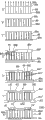
Fig. 1 illustrates the known method of the film-substrate that is used for handling sequence number " a "-" f ", so that from a kind of metal material, form the toroidal induction coil by the micro through hole that uses orientation to pass thin-film material;
Fig. 2 illustrates the induction coil of making according to the method for Fig. 1 with perspective illustration;
Fig. 3 illustrates the many through holes with relevant surfaces structural circuit in the induction coil, yet shows that the body material is removed;
Fig. 4 illustrates the electroheat pair of the basis regulation relevant with the present invention with perspective illustration;
Fig. 5 is illustrated in according in the application of the present invention with curve, can be assigned to the temperature difference relevant with the time of the cold junction point of the hot junction of thermocouple and thermocouple;
Fig. 6 illustrates the variation relevant with the time of temperature difference, and this variation is corresponding to voltage that is provided by thermocouple or electromotive force (EMF);
Fig. 7 illustrates the curve of the relation between the selected thickness of representing film-substrate and the time point that produces maximum temperature difference;
Fig. 8 is in the order of a method shown in a plurality of processing steps, and it is similar to order shown in Figure 1, so that from being configured to the body material of film, can form occasionally other circuit arrangement of thermoelectricity by at least two kinds of different metal materials;
Fig. 9 an optional method shown in a plurality of processing steps order, it is similar to order shown in Figure 8;
Figure 10 illustrates the replacement scheme that is used for preceding two treatment steps of Fig. 9 are combined into single treatment step.
The description of prior art
Referring to figs. 1 to 3, in Fig. 1, the method for previously known is shown handles film-substrate according to the technology prerequisite of in the publication of mentioning by introduction, being seen here so that in a plurality of processing steps, allow.
Like this, proposed order shown in Figure 1 so as with " a " extremely " f " in the different process step represented, allow to handle film-substrate 1, thereby the Printed Circuit Card 2 in by this way can production drawing 2, its have by or be arranged to pass completely through film-substrate 1 and back to a plurality of micro through holes of being electrically connected of surperficial 1a, 1b so that can form circuit arrangement with the form of helix tube induction coil 2a by this way.
For the purpose of simplifying, five micro through holes of utilization by " V1 ", " V2 " to " V5 " expression only are shown in Fig. 2, need to be far longer than quantity in actual applications shown in this, and close far away in the structure shown in this.
In Fig. 1 a, about this point, illustrate with the form of ion " J " and utilize accelerated particle to handle whole film-substrate 1, form many nano wire 1d or potential nanometer path 1d by penetrating of these ions.
As ion " J ", can advantageously utilize 1000MeV
129Xe
27+, it is proved to be the plastics that are suitable for passing the polyimide structures that adopts film-substrate 1 form.
In Fig. 1 a, film-substrate is by first top thin copper layer 1 ' and the second following thin copper layer 1 " cover.
Fig. 1 b illustrates the top side 1 ' and the bottom side 1 of film-substrate 1 ", be coated with layer of copper layer 12 and 13 and go up copper layer 12 and be provided with opening 12a separately.
More specifically, handle copper layer 12 so that limit contiguous expectation micro through hole, such as the through hole among Fig. 2 " V1 ", opening 12a.
Thereby in Fig. 1 c, handle nano wire 1d and form real nanometer path 1e.
Speed when Fig. 1 c also is intended to illustrate with described ion or particle " J " bombarded surface part, to such an extent as to mutually adjusting such value with the quality of particle can select and the relevant kinetic energy of particle " J ", thereby at least some particles thoroughly pass described film-substrate 1 fully definitely, form many nano wire 1d or pass through the potential nanometer path of described film-substrate fully so that allow like this.
Fig. 1 d illustrates described real nanometer path 1e and is filled with the metal material 1f with fabulous conductive characteristic in known manner, is used to form and the relevant micro through hole of boring a hole, for example through hole " V1 ".
In addition, Fig. 1 d illustrates with two steps and by usually said electro-deposition nickel or copper is deposited in hole or the real nanometer path 1e.
Because hole or real nanometer path 1e are to lower floor 1 " extend through the whole thickness of film-substrate 1, this can be made of support section, perhaps utilizes adhesive tape.
In Fig. 1 c, also can use ethanol to realize the prerinse in perforation or real nanometer path, so that improve moistening (wetting) in real nanometer path.
In Fig. 1 e, be illustrated in material and go up copper layer 1 ' before through electro-deposition arrival, be removed.
First electro-deposition is suitable for being used for protecting copper layer or copper film 1 " be not subjected to the influence of etching solution.
Carry out electro-deposition then.
When micro through hole " V1 " during towards the upper surface 1a of film-substrate 1 growth, form " cup " and stop etching.
Fig. 1 f also illustrate can by one or both be applied to film-substrate on the surface as circuit and have the material of conductive characteristic, a described through hole " V1 " relevant with perforation becomes electrical interconnection now.
Fig. 1 f can illustrate thin golden film 1g in this respect and be deposited in that upper surface 1a goes up and copper film 1h is applied on this thin golden film 1g.
Now can be by the required circuit on the isotope wet etching generation top side (and bottom side).
Here, Fig. 2 illustrates an induction coil, five through holes have only been shown, it has required first lead on the upper surface 1a of the film-substrate of being applied to, here use " L1 ", " L3 " and " L5 " expression, and connect so that, through hole " V1 ", " V2 " are set in the induction coil to being connected in series of " V5 " by using second lead on the surperficial 1b that is applied to film-substrate of " L2 ", " L4 " and " L6 " expression here.
Here, Fig. 3 illustrates the outward appearance of described through hole " V2 ", " V3 " and " V4 " substantially, and the mode that shows with Fig. 2 of the circuit on the top side " L3 ", " L5 " illustrates the micro through hole of interconnection, and circuit " L4 " is positioned on the 1b of bottom side in addition.
All leads on the 1a of top side, the micro through hole that all pass film-substrate and all leads on the bottom side are all by forming with a kind of metal material.The explanation of the embodiment of Ti Chuing now
Emphasize in the mode of introducing then: in the explanation of present embodiment subsequently, it has the key character relevant with the present invention and by showing that Fig. 4 to 10 in the accompanying drawings is described, selecting vocabulary and specific term at the present invention mainly is in order to make basic thought of the present invention clearer.
Yet, should consider here about this point that the expression way of selecting should not be regarded as and only be confined to the term that utilizes and select here, to such an extent as to but should be appreciated that should explain selection like this like this each term it comprise all technical equivalents in addition with identical or basic identical mode work so that can realize identical or essentially identical invention and/or technique effect like this.
Like this, with reference to figure 4, schematically illustrated primary condition of the present invention of processing and requirement by existing embodiment that proposes and suitable present proposition, make important feature relevant or feature more concrete with the present invention, below by Fig. 4 to 10 described embodiment and processing are shown in further detail in the accompanying drawings, and are described in more details in the following description.
Like this, the present invention is in principle based on the method that is used for another technical field with in the application shown in Fig. 1 to Fig. 3, wherein need the many places adjustment, so that can provide one or more circuit settings by this technology, below be that example describes with the thermocouple, it is suitable for use as detector in the application that is used for gasmetry.
About this point, the present invention has told about the real nanometer path 1e of first quantity, here be example with three, should be filled with the first material M1 with good electrical characteristics, be used for according to first micro through hole that forms first quantity in the main mode that shows of Fig. 1 e, with " V10 ", " V30 " and " V50 " expression in this name.
Yet, the present invention tells about or advises the real nanometer path of second quantity, here be example with three, should be filled with the second material M2 with good electrology characteristic, be used to form second quantity, second micropore in this name, with " V20 ", " V40 " and " V50 " expression, can influence it according to the main mode that shows in Fig. 1 e then, yet, under the situation that should cover first through hole " V10 ", " V30 " and " V50 " with mask, should come out so that the second material M2 can enter in the second real nanometer path.
In Fig. 8,9 and 10, be clearly shown that more and described relevant therewith method and processing step, below will be described in further detail.
Till during to thermocouple, the first material M1 and the second material M2 for described first and second micro through holes that importantly should select to have different mutually electric heating characteristics the illustrated embodiment according to the present invention, the electroheat pair that is used to form one or more coordinations or separates, it provides electromotive force under the temperature difference between heat (10a) and cold (10b) node.
About this point, the present invention is based on understanding when different metal is bonded to each other end-to-end under the temperature difference, and they have different electric heating characteristics.
Like this, by known experiment, the present invention is based on the pyroelecthc properties of wanting that allows to determine to want between the material.
The surface is applied 10a and 10b distribute and adjust, so that allow to be appointed as first micro through hole " V10 ", " V30 " and " V50 " of the first material M1 and be appointed as second micro through hole " V20 " of the second material M2, the electrical interconnection of " V40 " and " V50 " by formed circuit L10, L30 and L50 to the electric conducting material that is coated in film-substrate 10 both sides of film-substrate 10.
Be included in being connected in series first micro through hole " V10 " be included in last micro through hole " V50 " in being connected in series be coordination so that form the electroheat pair that is connected in series through being connected 101 and 102.
Not only Fig. 2, and Fig. 4 also only illustrates according to the sub-fraction of inductance of the present invention or the sub-fraction of electroheat pair 100, and is to be understood that in order to form thermocouple 100, can and should be one another in series to connect the micro through hole of quite big quantity.
On identical thin-film material 1, do not get rid of a plurality of individual thermoelectric idols that are connected in series according to Fig. 4 of formation.
Do not get rid of and allow to be connected in parallel a plurality of this thermocouples that independently are connected in series 100.
The film-substrate 10 of the processing shown in Figure 4 of electroheat pair 100 is fit to be included in the detector that is suitable for spectrum analysis as signal receiver.
For those skilled in the art, it is evident that the surface portion 10a that can on film-substrate 10, repeat electroheat pair 100, as reference number 10a ', two electroheat pairs 100 and 100 ' can be positioned on the same film-substrate 10 thus, wherein described thermocouple 100 can be respectively applied for different light or ripple with 100 ' during spectrum analysis, wherein thermocouple 100 can be used for accurate measurement, thermocouple 100 ' can be used as reference measure, and two signals can be transported to the electronics numerical value counting circuit that is essentially known type through described connecting line.
According to Fig. 4, drop on and in the scope of the invention be, selection part or whole outer surface 10a as the film-substrate 10 of body material should handle with heavy accelerated particle " J ", so that so not only for the different metal that uses some micro through hole to be used to be interconnected as electroheat pair creates conditions, and equally can be in film-substrate, forming another circuit with form known and the circuit setting creates conditions.
According to the present invention and its application in this explanation, requirement should select to be assigned to the kinetic energy of particle or ion so that all particles of at least 80% will pass the selected thickness of described film-substrate 10 fully definitely, ideally connects by thin substrate so that can guarantee the micro through hole of coordination like this.
Because the present invention is based on the possibility that is connected in series of a plurality of micro through holes with mutual identical or different material, electrically contact so pass fully up or down to arrive the surface and provide, require to be certain to be connected in series like this through established surperficial interlock circuit with the relevant micro through hole of boring a hole at micro through hole.
In addition according to the present invention; described real nanometer path can form (this result compares with a plurality of embroideries (embroidery) on the surf zone relevant with described thin substrate) by mask or protuberance technology; under the sort of situation; the selected real nanometer path of first quantity; through the technology of selection with by mask, becoming is filled with first electric conducting material so that form first micro through hole.
Yet, the selected real nanometer path of second quantity should also be filled with second electric conducting material so that form second micro through hole through the technology of selection with by mask, and make described first through hole and the described second through hole coordination, when they are interconnected as electroheat pair and/or circuit arrangement with box lunch, show desirable characteristic.
Like this, the present invention has also illustrated and make a plurality of first micro through holes and a plurality of second micro through hole electrical interconnection by the electric conducting material in two surfaces that are applied to film-substrate through mask or protuberance, has been used to form tangible lead and circuit.
In addition, illustrated and make a plurality of first micro through holes and a plurality of second micro through hole electrical interconnection by the electric conducting material on the second surface in two surfaces that are applied to film-substrate through mask or protuberance, be used to form tangible lead and circuit.
Do not get rid of described lead and circuit and form simultaneously, the circuit that passes through through other micro through hole in film-substrate also is provided, in other circuit arrangement, comprise described through hole as circuit so that allow.
Described film-substrate 10 is selected from plastic material, and thickness is specified between the 200 and 30 μ m, preferably between 120 μ m and 50 μ m, so that can provide electroheat pair like this, will illustrate in greater detail its essence below.Thickness should be able to be chosen between the 100 and 75 μ m.
More specifically, described film-substrate 10 can comprise the aromatic polymer material, carries out etching under alkalescence and/or wet oxidation environment, utilizes chemical agent to be used to form real nanometer path simultaneously.
More specifically, point out kinetic energy should be chosen in 200 and the every ion of 7000MeV between, wherein have and select deterministic ion, be set at least 80% here, should be able to pass the thickness of film-substrate 10.
The described nano wire 1d that in film-substrate 10, produces can by " Coulomb " blast and/or thermal transient phenomenon subsequently form, in its described in front communique 18 pages have and show in further detail and illustrate.
For example handle the potential nano wire or the nanometer path 1d of passing through of described selection in known manner, pass through the real nanometer path of film-substrate 10, wherein can utilize the solution that contains clorox or contain potassium oxide, be used for this processing so that form.
In addition, illustrated for inner track and should be able to for example utilize ethanol to carry out preliminary treatment, be used for wetting interior pathway surfaces really passing through opening nanometer path 1e.
With reference to figure 5, illustrate at temperature that is assigned to hot junction and the temperature-time curve that is assigned to the temperature of cold junction point, described hot junction and cold junction point are located on the thermocouple that is used as detector in the spectrum analysis, and wherein the temperature difference of appointment " dT " can be considered to depend on following at least factor:
A) facing to the luminous intensity of the light wave of upper surface 10a incident,
B) frequency of the luminous intensity between two continuous impulses,
C) the last gradient feature of luminous intensity,
D) pass through the micro through hole length " d " of film-substrate 10,
E) pass through the calculated thickness " t " of the micro through hole of film-substrate 10,
F) distance between the adjacent micro through hole, distance " a " (Fig. 3) are equal to distance between through hole " V2 " and " V3 ", and are equal to distance between through hole " V2 " and " V4 " apart from " a1 ",
G) heat taking place passes between micro through hole and body material,
H) material of in body material or film-substrate 10, selecting,
I) selected 103 heat conduction from lower surface 10b to bottom,
J) quantity in the real nanometer path that when forming micro through hole separately, is connected in parallel,
K) calculated thickness in described real nanometer path.
Illustrate with showing according to the embodiment of Fig. 4 and to utilize many different parameters, each parameter all is suitable for electroheat pair.
The length that increases micro through hole " V10 " and other micro through hole is very natural, undeniable ground, this can demonstrate large-signal " V ", but also can provide the bigger delay that produces temperature difference, because the increase heat of the generation on surperficial 10a will pass through longer distance through the heat conduction to surperficial 10b.
Thicker micro through hole or the micro through hole that comprises too much real nanometer path have increased the heat conduction to surperficial 10b.
Many thin micro through holes provide the bigger heat conduction to the body material than having the long-pending thicker micro through hole of same cross-sectional.Single thick micro through hole provides lower temperature gradient than a large amount of thin micro through holes.
The thin thicker micro through hole of micro through hole provides higher resistance value.
The micro through hole of the larger amt that is connected in series in this way, fewer micro through hole provides higher output signal.
Additional parameter can be assigned to it with the condition of electroheat pair, is that the characteristic relevant with the time of employed light source or lamp can influence temperature difference.
Yet if prove that the frequency that will launch light pulse thus is assigned to this lamp by pulse control lamp, should select this frequency to make it appear at thickness " d " during 0.1 second is 100
The film-substrate place of μ m.
Another condition is that micro through hole should have predetermined resistance value, and wherein same value should be low as much as possible, such as being lower than 100 Ω, yet reaches or the resistance value that equals the electroheat pair of 30-50k Ω also can be accepted.
The time change that Fig. 6 illustrates temperature difference makes progress, and wherein said curve also can be taken as the output signal of expression from electroheat pair 100.
In Fig. 7, how relevant, how relevant with the repetition rate of employed light source or lamp with output signal from electroheat pair curve illustrates the height dimension of film-substrate or thickness " d ".
According to the present invention, should advantageously construct electroheat pair to form even number micro through hole or coordination micro through hole, half is formed by first material, material M1 for example, half is formed by second material, for example material M2.
In a word, can mention real nanometer path and micro through hole should be thin as much as possible in practice, and employed metal material should have alap thermal conductivity.
Material should have big as far as possible Seebeck-effect, thermoelectric effect or electromotive force (EMF) to M1 and M2.
Within the scope of the invention, in micro through hole and/or for surface portion 10a and 10b, use conduction or semiconductive material fully respectively as much as possible certainly,, can construct different circuit settings so that like this when at least two kinds of different materials of utilization.
For the circuit of 10a and 10b surfacewise respectively, do not get rid of and select the metal material different with the material that in micro through hole, uses.
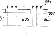
In Fig. 8, the order that is similar to shown in Fig. 1 is shown, one has been divided into many steps " A ", " B " extremely " G " method, so that by being configured to the body material of film, using at least two kinds, three be three kinds of different metal material M1, M2 and M3 here during, can form occasionally another circuit arrangement of thermoelectricity.
Like this, Fig. 8 A illustrates when using particle or ion 80a, and body material 80 is exposed in the radiation with the form of thin-film material, forms thus and passes through nano wire 80b or potential nanometer path 80b.
Here, according to the prior art in the same process step, the whole top surface 80c of processing material 80 and nano wire 80b become and evenly distribute.
Fig. 8 B is illustrated in the nano wire 80b that forms among Fig. 8 A and carries out etch processes so that real nanometer path 80d is provided in a processing step.
Here, thus handle the intensive perforation that whole top surface 80c body material 80 shows real nanometer path 80d.
In Fig. 8 C, the material of handling according to Fig. 8 B 80 is shown in other processing step, prepares metal level 80e is arranged.
Fig. 8 D is illustrated in the processing step, will have the photoresist of mask and opening 80g, and dry film 80f is applied on the top surface 80c, so that expose real nanometer path 80h shown in three.
By comprising the electroplating technique step, apply metal material " M1 " so that identical materials is filled nanometer path 80h and is distributed in the opening 80g.
Fig. 8 D also illustrates the resist 80i as mask or diaphragm is applied to metal level 80e.
Fig. 8 E is illustrated in subsequently the processing step, removes dry film 80f, and will have the photoresist of opening 80g ', and dry film 80f ' is applied on the top surface 80c, so that expose real nanometer path 80h ' shown in three.
Comprise the electroplating technique step by what repeat, apply metal material " M2 " so that identical materials is filled nanometer path 80h ' and is distributed in the opening 80g '.
Fig. 8 F is intended to be illustrated in the processing step and has removed film 80f ', and the new photoresist 80j that in step subsequently, will have the mask that has opening 80k, dry film, be applied on the top surface 80c, so that the nanometer path 80h of exposure filling and 80h ' are as micro through hole respectively, and apply metal material M3 to form required circuit by plating, for example by the circuit of " L10 " expression.
Fig. 8 F also is intended to be illustrated in and removes metal level 80e and diaphragm 80i ' in the processing step; and the new photoresist 80j ' that in step subsequently, will have the mask that adopts opening 80k ' form; dry film; be applied to basal surface 80c '; so that the nanometer path 80h of exposure filling and 80h ' are as micro through hole respectively; and apply metal material M3 to form required circuit by plating, for example in Fig. 4 by the circuit of " L30 " expression.
Fig. 8 G is illustrated in the processing step, has removed photoresist 80j and 80j ', and circuit arrangement (100) is near completion thus, the micro through hole on the top side 80c that this circuit arrangement makes film 80 and the bottom side 80c ' and the electric each other combination of circuit be connected.
In another embodiment, can from the metal material with conductivity select material " M1 ", " M2 ", " M3 " and " M4 " and make its identical or from material and/or from material, select material " M1 ", " M2 " with semiconduction with different conductivity, " M3 " is with " M4 " and make them different mutually.
And some that is covered by metal material is shown not Fig. 8 G and real nanometer path 80m, the 80m ' that selects can be as ventilating and cooling water pipe.
In Fig. 9, the order that is similar to shown in Fig. 8 is shown, a method that is divided into many steps " A ", " B " to " F ", so that by being configured to the body material of film, using at least two kinds, here be during three kinds of different metal material M1, M2 and M3, can form occasionally other circuit arrangement of thermoelectricity.
Like this, Fig. 9 A illustrates when using particle or ion 80a, and body material 80 is exposed in the radiation with the form of thin-film material, and nano wire 80b or potential nanometer path 80b are passed through in formation thus.
Here, according to the prior art in the same process step, the whole top surface 80c of processing material 80 and nano wire 80b become and evenly distribute.
Fig. 9 B illustrates by photoresist 80f and covers the nano wire 80b that forms among Fig. 9 A through mask and its opening 80g, and they carry out etch process in according to the processing step of Fig. 9 C, so that the real nanometer path 80d of selection is provided.
Here, only handle the selection part of top surface 80c, thereby body material 80 presents the selection perforation of real nanometer path 80d.
In Fig. 9 B and 9C, being illustrated in the other processing step material 80 preparations has metal level 80e.
Fig. 9 D is illustrated in the processing step, will have the photoresist of opening 80g, and dry film 80f is applied to top surface 80c, so that expose real nanometer path 80h shown in three.
By comprising the electroplating technique step, apply metal material " M1 " so that identical materials is filled nanometer path 80h and is distributed in the opening 80g.
Fig. 9 E is illustrated in subsequently the processing step, removes dry film 80f, will have the photoresist of opening 80g ', dry film 80f ", be applied to top surface 80c, so that expose real nanometer path 80h ' shown in three.
By comprising the iterative process step of plating, apply metal material " M2 " so that identical materials is filled nanometer path 80h and is distributed in the opening 80g '.
, after the step of Fig. 9 F, therefore do not illustrate here according to the processing step shown in the front of Fig. 8 F and 8G.
Figure 10 is intended to the radiation that influences ion 80a by mask process or protuberance is shown, and is formed in the surface portion with only potential nanometer path and nano wire 80b, after above-mentioned treatment step, forms micro through hole.
Even show that the present invention is relevant with thermocouple, it is evident that described technology also can be used for other detector, for example IR detector, moving detector etc.
The present invention is not limited to the above-mentioned embodiment that provides as an example certainly, but can revise in the scope according to the basic thought of the present invention that illustrates in the claims subsequently.
Especially, should consider that described within the scope of the invention each unit can be bonded to each other so that obtain the desired techniques function.
Claims (36)
1, a kind of film-substrate of the processing for production printed circuit card or plate, have a plurality of by or pass described film-substrate, and connect to form the micro through hole of circuit, wherein back to surface electrical along two of described film-substrate; A; Utilize accelerated particle to handle the surface portion of some selection at least of film-substrate; B; When the surface portion of the described selection of described particle bombardment, to such an extent as to described particle's velocity should be mutually adjusted such value with quality and select the kinetic energy relevant with particle, thereby make at least some described particles can pass described film-substrate fully definitely, pass through the nano wire or the potential nanometer path of described film-substrate so that allow like this to form; C; For example the real nanometer path of this film-substrate is passed through so that form in the treatment of selected potential nanometer path of passing through of selecting in a known way; D; Itself to be that known method makes described real nanometer path be filled with the material with selected conductive characteristic, be used to form the perforation micro through hole; E; A plurality of perforation micro through holes by a kind of or two kinds be applied to this film-substrate on the surface and the material with selected conductive characteristic carry out electrical interconnection, the described real nanometer path of first quantity is filled with first material (M1) with selected electrical characteristics, be used to form the first through hole (V10 in this name of first quantity, V30, V50), and the described real nanometer path of second quantity is filled with second material (M2) with selected electrical characteristics, be used to form the second through hole (V20 in this name of second quantity, V40, V60), be characterised in that (described first material (M1) of V1-V60) selects to make described first material and described second material to have different electrical characteristics mutually with described second material (M2) to selected first and second through holes, distribute and/or adjust the surface is applied to this film-substrate and be coated in the material on these film-substrate both sides so as first through hole that has allowed to distribute described first material with distributed the second through hole electrical interconnection of described second material, and make first through hole (V10) that is included in being connected in series and be included in last through hole (V60) coordination in described being connected in series so that electroheat pair and/or circuit arrangement to be provided.
2, the film-substrate of processing according to claim 1, wherein said accelerated particle adopts ionic species.
3, the film-substrate of processing according to claim 1, be characterised in that the film-substrate of handling is fit to be included in the detector that is suitable for spectrum analysis as signal receiver, the height dimension of wherein said film-substrate or thickness are relevant with output signal from described electroheat pair.
4, the film-substrate of processing according to claim 1 is characterised in that, during " a ", utilizes heavy speeding-up ion to handle the outer surface of described whole film-substrate.
5, the film-substrate of processing according to claim 1 is characterised in that during " b ", determines to pass described film-substrate to such an extent as to the described particle of the kinetic energy at least 80% of particle or ion is distributed in selection.
6, the film-substrate of processing according to claim 1 is characterised in that during " c ", forms described real nanometer path by mask process.
7, the film-substrate of processing according to claim 1 is characterised in that during " d ", and selected real nanometer path is filled with first material so that form first through hole by electroplating technology.
8, the film-substrate of processing according to claim 1 is characterised in that during " d ", and the second real nanometer path of selecting is filled with second material so that form second through hole by electroplating technology.
9, the film-substrate of processing according to claim 1 is characterised in that during " e ", and a plurality of first through holes and a plurality of second through hole are by being applied to the material electrical interconnection in two surfaces of this film-substrate through mask process.
10, the film-substrate of processing according to claim 1 is characterised in that during " e ", and a plurality of first through holes and a plurality of second through hole are by second lip-deep material electrical interconnection in two surfaces that are applied to this film-substrate through mask process.
11, the film-substrate of processing according to claim 1, be characterised in that during " b ", the potential nanometer path of passing through that limits comprises that at first nano wire form with anisotropic material is formed on the coordination nano wire in the described film-substrate, and the effect that this nano wire is easy to be subjected to chemical etching is used to form real nanometer path.
12, the film-substrate of processing according to claim 1 is characterised in that described film-substrate is selected from the thickness between plastic material and given 200 μ m and the 30 μ m.
13, according to the film-substrate of claim 1 or 12 described processing, be characterised in that described film-substrate is formed by the aromatic polymer material, when utilizing chemical agent to form the real nanometer of opening path, under alkalescence and/or wet oxidation environment, carry out etching.
14, the film-substrate of processing according to claim 1 is characterised in that during " b ", with described kinetic energy be chosen in 200 and the every ion of 7000MeV between.
15, the film-substrate of processing according to claim 1 is characterised in that during " b ", provides described nano wire by " Coulomb " blast and/or by the thermal transient phenomenon.
16, the film-substrate of processing according to claim 1 is characterised in that during " c ", uses the solution that comprises clorox or potassium oxide.
17, the film-substrate of processing according to claim 1 is characterised in that the described real nanometer path that preliminary treatment forms during " c ", be used for wetting interior pathway surfaces.
18, the film-substrate of processing according to claim 17, wherein said preliminary treatment utilize ethanol to carry out.
19, a kind of method that is used to handle for the film-substrate of production printed circuit card or plate, this film-substrate have a plurality of by or pass described film-substrate, and connect to form the micro through hole of circuit, wherein back to surface electrical along two of described film-substrate;
A; Utilize accelerated particle to handle the surface portion of some selection at least of described film-substrate;
B; When the surface portion of the described selection of described particle bombardment, to such an extent as to described particle's velocity should be mutually adjusted such value with quality and select the kinetic energy relevant with particle, thereby make at least some described particles can pass described film-substrate fully definitely, pass through the nano wire or the potential nanometer path of described film-substrate so that allow like this to form;
C; For example the real nanometer path of this film-substrate is passed through so that form in the treatment of selected potential nanometer path of passing through of selecting in a known way;
D; Itself to be that known method makes described real nanometer path be filled with the material with selected conductive characteristic, be used to form the perforation micro through hole;
E; A plurality of perforation micro through holes by a kind of or two kinds be applied to this film-substrate on the surface and the material with selected conductive characteristic carry out electrical interconnection, the described real nanometer path of first quantity is filled with first material (M1) with selected electrical characteristics, be used to form the first through hole (V10 in this name of first quantity, V30, V50), and the described real nanometer path of second quantity is filled with second material (M2) with selected electrical characteristics, be used to form the second through hole (V20 in this name of second quantity, V40, V60)
Be characterised in that (described first material (M1) of V10-V60) is selected with described second material (M2) so that described first material has mutually different electrical characteristics with described second material to selected first and second through holes; Distribute and/or adjust the surface is applied to this film-substrate and be coated in the material on these film-substrate both sides so as first through hole that has allowed to distribute described first material with distributed the second through hole electrical interconnection of described second material, and make first through hole (V10) that is included in being connected in series and be included in last through hole (V60) coordination in described being connected in series so that electroheat pair and/or circuit arrangement to be provided.
20, method according to claim 19, wherein said accelerated particle adopts ionic species.
21, method according to claim 19, be characterised in that the film-substrate of handling is fit to be included in the detector that is suitable for spectrum analysis as signal receiver, the height dimension of wherein said film-substrate or thickness are relevant with output signal from described electroheat pair.
22, method according to claim 19 is characterised in that during " a ", utilizes heavy speeding-up ion to handle the outer surface of described whole film-substrate.
23, method according to claim 19 is characterised in that during " b ", determines to pass described film-substrate to such an extent as to the described particle of the kinetic energy at least 80% of particle or ion is distributed in selection.
24, method according to claim 19 is characterised in that during " c ", forms described real nanometer path by mask process.
25, method according to claim 19 is characterised in that during " d ", and selected real nanometer path is filled with first material so that form first through hole by electroplating technology.
26, method according to claim 19 is characterised in that during " d ", and the second real nanometer path of selecting is filled with second material so that form second through hole by electroplating technology.
27, method according to claim 19 is characterised in that during " e ", and a plurality of first through holes and a plurality of second through hole are by being applied to the material electrical interconnection in two surfaces of this film-substrate through mask process.
28, method according to claim 19 is characterised in that during " e ", and a plurality of first through holes and a plurality of second through hole are by second lip-deep material electrical interconnection in two surfaces that are applied to this film-substrate through mask process.
29, method according to claim 19, be characterised in that during " b ", the potential nanometer path of passing through that limits comprises that at first nano wire form with anisotropic material is formed on the coordination nano wire in the described film-substrate, and the effect that this nano wire is easy to be subjected to chemical etching is used to form real nanometer path.
30, method according to claim 19 is characterised in that described film-substrate is selected from the thickness between plastic material and given 200 μ m and the 30 μ m.
31, method according to claim 19 is characterised in that described film-substrate is formed by the aromatic polymer material, when utilizing chemical agent to form the real nanometer of opening path, carries out etching under alkalescence and/or wet oxidation environment.
32, method according to claim 19 is characterised in that during " b ", with described kinetic energy be chosen in 200 and the every ion of 7000MeV between.
33, method according to claim 19 is characterised in that during " b ", provides described nano wire by " Coulomb " blast and/or by the thermal transient phenomenon.
34, method according to claim 19 is characterised in that during " c ", uses the solution that comprises clorox or potassium oxide.
35, method according to claim 19 is characterised in that the described real nanometer path that preliminary treatment forms during " c ", be used for wetting interior pathway surfaces.
36, method according to claim 35, wherein said preliminary treatment utilize ethanol to carry out.
Applications Claiming Priority (2)
| Application Number | Priority Date | Filing Date | Title |
|---|---|---|---|
| SE03012382 | 2003-04-29 | ||
| SE0301238A SE526006C2 (en) | 2003-04-29 | 2003-04-29 | Treated thin film substrate |
Publications (2)
| Publication Number | Publication Date |
|---|---|
| CN1781350A CN1781350A (en) | 2006-05-31 |
| CN100521876C true CN100521876C (en) | 2009-07-29 |
Family
ID=20291147
Family Applications (1)
| Application Number | Title | Priority Date | Filing Date |
|---|---|---|---|
| CNB2004800116430A Active CN100521876C (en) | 2003-04-29 | 2004-04-21 | Method for processing a thin film substrate |
Country Status (10)
| Country | Link |
|---|---|
| US (1) | US7176578B2 (en) |
| EP (1) | EP1621054B1 (en) |
| JP (1) | JP4359657B2 (en) |
| KR (1) | KR101055600B1 (en) |
| CN (1) | CN100521876C (en) |
| AT (1) | ATE524956T1 (en) |
| AU (1) | AU2004234763B2 (en) |
| CA (1) | CA2523971A1 (en) |
| SE (1) | SE526006C2 (en) |
| WO (1) | WO2004098256A1 (en) |
Families Citing this family (13)
| Publication number | Priority date | Publication date | Assignee | Title |
|---|---|---|---|---|
| EP1832146A1 (en) * | 2004-12-28 | 2007-09-12 | Siemens Home and Office Communication Devices GmbH & Co. KG | Semifinished product and support component based on said semifinished product |
| JP4344954B2 (en) | 2006-10-03 | 2009-10-14 | セイコーエプソン株式会社 | Method for manufacturing element substrate |
| WO2008063125A1 (en) * | 2006-11-20 | 2008-05-29 | Senseair Ab | A process for treating a flexible thin film substrate, in the form of a dielectric plastic foil, and a thin film substrate thus formed |
| US20090162666A1 (en) * | 2007-12-20 | 2009-06-25 | Palo Alto Research Center Incorporated | Curable flexible material |
| US20090223700A1 (en) * | 2008-03-05 | 2009-09-10 | Honeywell International Inc. | Thin flexible circuits |
| US7884488B2 (en) * | 2008-05-01 | 2011-02-08 | Qimonda Ag | Semiconductor component with improved contact pad and method for forming the same |
| US8026567B2 (en) * | 2008-12-22 | 2011-09-27 | Taiwan Semiconductor Manufactuirng Co., Ltd. | Thermoelectric cooler for semiconductor devices with TSV |
| JP2011233714A (en) * | 2010-04-27 | 2011-11-17 | Canon Inc | Semiconductor device |
| US20150035162A1 (en) * | 2013-08-02 | 2015-02-05 | Qualcomm Incorporated | Inductive device that includes conductive via and metal layer |
| SE541450C2 (en) | 2018-02-19 | 2019-10-08 | Jondetech Sensors Ab Publ | Overheating alarm device for cell phone charger or similar device |
| SE543173C2 (en) | 2018-07-02 | 2020-10-20 | Jondetech Sensors Ab Publ | Adapter device with infrared sensor and heat protection switch |
| US20200361782A1 (en) * | 2019-05-16 | 2020-11-19 | Sciosense B.V. | Photo-annealing in Metal Oxide Sensors |
| US11662109B2 (en) | 2019-06-05 | 2023-05-30 | Carrier Corporation | Enclosure for gas detector |
Family Cites Families (4)
| Publication number | Priority date | Publication date | Assignee | Title |
|---|---|---|---|---|
| SE521415C2 (en) * | 1998-02-17 | 2003-10-28 | Hans Goeran Evald Martin | Method for producing a gas sensor-associated detector, as well as a detector made according to the method |
| JP3655242B2 (en) * | 2002-01-04 | 2005-06-02 | 株式会社東芝 | Semiconductor package and semiconductor mounting apparatus |
| US6891266B2 (en) * | 2002-02-14 | 2005-05-10 | Mia-Com | RF transition for an area array package |
| TWI256719B (en) * | 2002-03-06 | 2006-06-11 | Via Tech Inc | Semiconductor device package module and manufacturing method thereof |
-
2003
- 2003-04-29 SE SE0301238A patent/SE526006C2/en not_active IP Right Cessation
-
2004
- 2004-04-21 KR KR1020057020583A patent/KR101055600B1/en active IP Right Grant
- 2004-04-21 AU AU2004234763A patent/AU2004234763B2/en active Active
- 2004-04-21 CA CA002523971A patent/CA2523971A1/en not_active Abandoned
- 2004-04-21 CN CNB2004800116430A patent/CN100521876C/en active Active
- 2004-04-21 WO PCT/SE2004/000606 patent/WO2004098256A1/en active Application Filing
- 2004-04-21 EP EP04728728A patent/EP1621054B1/en active Active
- 2004-04-21 AT AT04728728T patent/ATE524956T1/en not_active IP Right Cessation
- 2004-04-21 JP JP2006508027A patent/JP4359657B2/en not_active Expired - Fee Related
-
2005
- 2005-10-26 US US11/258,763 patent/US7176578B2/en active Active
Also Published As
| Publication number | Publication date |
|---|---|
| CA2523971A1 (en) | 2004-11-11 |
| AU2004234763A1 (en) | 2004-11-11 |
| SE0301238L (en) | 2004-10-30 |
| ATE524956T1 (en) | 2011-09-15 |
| EP1621054A1 (en) | 2006-02-01 |
| JP4359657B2 (en) | 2009-11-04 |
| SE0301238D0 (en) | 2003-04-29 |
| KR20060016761A (en) | 2006-02-22 |
| JP2007529101A (en) | 2007-10-18 |
| AU2004234763B2 (en) | 2008-07-24 |
| US7176578B2 (en) | 2007-02-13 |
| CN1781350A (en) | 2006-05-31 |
| US20060071323A1 (en) | 2006-04-06 |
| WO2004098256A1 (en) | 2004-11-11 |
| SE526006C2 (en) | 2005-06-14 |
| EP1621054B1 (en) | 2011-09-14 |
| KR101055600B1 (en) | 2011-08-09 |
Similar Documents
| Publication | Publication Date | Title |
|---|---|---|
| CN100521876C (en) | Method for processing a thin film substrate | |
| Huray et al. | Impact of copper surface texture on loss: A model that works | |
| DeDeo et al. | Effects of the sound speed of quintessence on the microwave background and large scale structure | |
| Bergmann et al. | Nonequilibrium in metallic microstructures in the presence of high current density | |
| US3334395A (en) | Method of making a metal printed circuit board | |
| US7200920B2 (en) | Method for the implementation of electronic components in via-holes of a multi-layer multi-chip module | |
| RU2006147225A (en) | MASS ANALYZER WITH ION TRAP | |
| CN105525918A (en) | Dual laterolog equipment, electrode system of dual laterolog equipment and formation resistivity measuring method | |
| EP3201954A1 (en) | Thermoelectric device | |
| US10240058B2 (en) | Reactively assisted ink for printed electronic circuits | |
| Ghiringhelli et al. | 3 d spin-orbit photoemission spectrum of nonferromagnetic materials: The test cases of CoO and Cu | |
| EP0164921A2 (en) | Improvements in and relating to printed circuit boards | |
| Suzuki | Nanoscale profile copper for high speed transmission printed wiring boards | |
| DE102013224068A1 (en) | Electronic module, method for operating such an electronic module and method for producing such an electronic module | |
| JPS5834958B2 (en) | Through-hole printed circuit board | |
| Glenzer et al. | Thomson scattering from two-species laser-produced plasmas | |
| Kim et al. | Depth-dependent temperature effects on thermoluminescence in multilayers | |
| Bolger et al. | Multi-layer PC boards Fabricated using Aerosol-jet Printing | |
| WO2008063125A1 (en) | A process for treating a flexible thin film substrate, in the form of a dielectric plastic foil, and a thin film substrate thus formed | |
| Barlow et al. | Report of the heavy flavours working group | |
| Lindeberg et al. | Flexible PCB vertical thermopile IR sensor | |
| Putterman | Phenomenological theory of collective modes and relaxation effects in type II superconductors | |
| Teyssier et al. | Three Temperatures Hydrodynamics of Cosmological Pancakes | |
| Lindeberg et al. | Ion track enabled high aspect ratio flexible PCB via technology | |
| DE102015214362A1 (en) | Microelectromechanical device |
Legal Events
| Date | Code | Title | Description |
|---|---|---|---|
| C06 | Publication | ||
| PB01 | Publication | ||
| C10 | Entry into substantive examination | ||
| SE01 | Entry into force of request for substantive examination | ||
| C14 | Grant of patent or utility model | ||
| GR01 | Patent grant | ||
| TR01 | Transfer of patent right |
Effective date of registration: 20180404 Address after: Stockholm Patentee after: Trond technology Sen Schell Address before: Dales Bbu, Sweden Patentee before: Senseair AB |
|
| TR01 | Transfer of patent right |