CN100524869C - Beam steering arrangements and optical switches - Google Patents
Beam steering arrangements and optical switches Download PDFInfo
- Publication number
- CN100524869C CN100524869C CNB02812202XA CN02812202A CN100524869C CN 100524869 C CN100524869 C CN 100524869C CN B02812202X A CNB02812202X A CN B02812202XA CN 02812202 A CN02812202 A CN 02812202A CN 100524869 C CN100524869 C CN 100524869C
- Authority
- CN
- China
- Prior art keywords
- exciter
- electrode layer
- electrode
- plate
- sawtooth
- Prior art date
- Legal status (The legal status is an assumption and is not a legal conclusion. Google has not performed a legal analysis and makes no representation as to the accuracy of the status listed.)
- Expired - Lifetime
Links
Images


Classifications
-
- G—PHYSICS
- G02—OPTICS
- G02B—OPTICAL ELEMENTS, SYSTEMS OR APPARATUS
- G02B6/00—Light guides; Structural details of arrangements comprising light guides and other optical elements, e.g. couplings
- G02B6/24—Coupling light guides
- G02B6/26—Optical coupling means
- G02B6/35—Optical coupling means having switching means
- G02B6/3564—Mechanical details of the actuation mechanism associated with the moving element or mounting mechanism details
- G02B6/3568—Mechanical details of the actuation mechanism associated with the moving element or mounting mechanism details characterised by the actuating force
- G02B6/3578—Piezoelectric force
-
- G—PHYSICS
- G02—OPTICS
- G02B—OPTICAL ELEMENTS, SYSTEMS OR APPARATUS
- G02B6/00—Light guides; Structural details of arrangements comprising light guides and other optical elements, e.g. couplings
- G02B6/24—Coupling light guides
- G02B6/26—Optical coupling means
- G02B6/32—Optical coupling means having lens focusing means positioned between opposed fibre ends
-
- H—ELECTRICITY
- H10—SEMICONDUCTOR DEVICES; ELECTRIC SOLID-STATE DEVICES NOT OTHERWISE PROVIDED FOR
- H10N—ELECTRIC SOLID-STATE DEVICES NOT OTHERWISE PROVIDED FOR
- H10N30/00—Piezoelectric or electrostrictive devices
- H10N30/20—Piezoelectric or electrostrictive devices with electrical input and mechanical output, e.g. functioning as actuators or vibrators
- H10N30/204—Piezoelectric or electrostrictive devices with electrical input and mechanical output, e.g. functioning as actuators or vibrators using bending displacement, e.g. unimorph, bimorph or multimorph cantilever or membrane benders
- H10N30/2041—Beam type
- H10N30/2042—Cantilevers, i.e. having one fixed end
- H10N30/2046—Cantilevers, i.e. having one fixed end adapted for multi-directional bending displacement
-
- H—ELECTRICITY
- H10—SEMICONDUCTOR DEVICES; ELECTRIC SOLID-STATE DEVICES NOT OTHERWISE PROVIDED FOR
- H10N—ELECTRIC SOLID-STATE DEVICES NOT OTHERWISE PROVIDED FOR
- H10N30/00—Piezoelectric or electrostrictive devices
- H10N30/50—Piezoelectric or electrostrictive devices having a stacked or multilayer structure
- H10N30/503—Piezoelectric or electrostrictive devices having a stacked or multilayer structure with non-rectangular cross-section orthogonal to the stacking direction, e.g. polygonal, circular
- H10N30/505—Annular cross-section
-
- H—ELECTRICITY
- H10—SEMICONDUCTOR DEVICES; ELECTRIC SOLID-STATE DEVICES NOT OTHERWISE PROVIDED FOR
- H10N—ELECTRIC SOLID-STATE DEVICES NOT OTHERWISE PROVIDED FOR
- H10N30/00—Piezoelectric or electrostrictive devices
- H10N30/80—Constructional details
- H10N30/87—Electrodes or interconnections, e.g. leads or terminals
- H10N30/871—Single-layered electrodes of multilayer piezoelectric or electrostrictive devices, e.g. internal electrodes
-
- G—PHYSICS
- G02—OPTICS
- G02B—OPTICAL ELEMENTS, SYSTEMS OR APPARATUS
- G02B6/00—Light guides; Structural details of arrangements comprising light guides and other optical elements, e.g. couplings
- G02B6/24—Coupling light guides
- G02B6/26—Optical coupling means
- G02B6/35—Optical coupling means having switching means
- G02B6/3502—Optical coupling means having switching means involving direct waveguide displacement, e.g. cantilever type waveguide displacement involving waveguide bending, or displacing an interposed waveguide between stationary waveguides
-
- G—PHYSICS
- G02—OPTICS
- G02B—OPTICAL ELEMENTS, SYSTEMS OR APPARATUS
- G02B6/00—Light guides; Structural details of arrangements comprising light guides and other optical elements, e.g. couplings
- G02B6/24—Coupling light guides
- G02B6/42—Coupling light guides with opto-electronic elements
- G02B6/4201—Packages, e.g. shape, construction, internal or external details
- G02B6/4219—Mechanical fixtures for holding or positioning the elements relative to each other in the couplings; Alignment methods for the elements, e.g. measuring or observing methods especially used therefor
- G02B6/422—Active alignment, i.e. moving the elements in response to the detected degree of coupling or position of the elements
- G02B6/4226—Positioning means for moving the elements into alignment, e.g. alignment screws, deformation of the mount
Abstract
An actuator comprises a laminate of interleaved layers of electrode plates and piezoelectric material; wherein an upper region (in use) of electrode plates is adapted when energised to effect deflections in up and down directions; a lower region of electrode plates is adapted when energised to effect deflections in up and down directions; and one or more further regions of electrode plates are adapted when energised to effect deflections in left and right directions.
Description
Technical field
The present invention relates to the device that a kind of its running is controlled by the pucker ﹠ bloat of piezoelectric.
Background technology
Main purpose of the present invention is to provide a kind of exciter that two-dimension displacement can be arranged.
Another object of the present invention is to provide a kind of its structure exciter of compactness especially.
Another object of the present invention is to provide a kind of can the repetition to turn round and keep the precision of running and the exciter of predictability simultaneously.Therefore a class exciter disclosed by the invention must be reliable.
Subsidiary purpose of the present invention is the new method that a kind of electrode configuration is provided in piezoelectric.
Other purpose of the present invention provides a kind of its shape can make exciter be easy to be assembled into exciter in the similar complete exciter.Therefore, another object of the present invention is to provide one group of compact especially and the same reliable exciter with the single exciter that is designed to work alone.
Summary of the invention
First independently aspect, the objective of the invention is a kind of integral type exciter that can in the time of an appointment, realize a large amount of angular displacements, this exciter is fixed on the supporting construction and in the Z direction and extends along length, and have a movably end, described exciter comprises the lamination that a battery lead plate and piezoelectric interweave; This exciter has first electrode layer; Encourage the device of described first electrode layer, thereby carry out terminal deflection in a direction, this direction is generally first Y direction; And the second electrode lay; Encourage the device of described the second electrode lay, thereby carry out terminal deflection in a direction, this direction is generally directions X; It is characterized in that each of exciter layer extended usually on the Z direction, and exciter comprises the third electrode layer, this third electrode layer and described first electrode layer separate along the Y direction; With the device of the described third electrode layer of excitation, thereby carry out terminal deflection in a direction, this direction is generally second Y direction.
Said structure is highly beneficial because its allow exciter with the X and the Y both direction upper deflecting of Z direction (the Z axle is in the direction of extending along the length of exciter) quadrature.The group compactness of these features.
Another subordinate aspect of first independent aspects is, exciter is a kind of common cylindric.
These aspects are very favourable, because it makes exciter attainable amplitude of oscillation maximization when crooked obtaining specific drive signal.In addition, the exciter of common cylinder shape is also very favourable, because it forms the array of a compactness when being particularly suitable on operation next door other similar exciter.
Another attached aspect, exciter comprises one or more passages.
Provide one or more passages highly beneficial, because the element that it can holding elongate, as optical fiber.In case these microscler elements are inserted in these passages, just can be with exciter deflection, and exciter can constitute the protection chamber of these elements.
Another subordinate aspect of first independent aspects is that the thickness of piezoelectric or each bar piezoelectric is in the scope of about 20 μ m~35 μ m.
In this specific scope, select strip of piezoelectric material very favourable, since the crooked maximum that in this scope, can reach, long-term simultaneously controllability and the reliability of keeping.
Another subordinate aspect of the present invention's first independent aspects is that electrode material or every strip electrode material have the thickness of about 2.5 μ m.
Under this thickness, the crooked maximum of exciter, long-term simultaneously controllability and the reliability of keeping.
Second independent aspects of the present invention is, a kind of pectination exciter that has made up two or more sawtooth is provided, and wherein one or more teeth comprise the lamination that a battery lead plate and piezoelectric interweave; Thereby wherein when exciter be energized when above-below direction carries out deflection battery lead plate above (in the use) zone adapted; Thereby the lower zone that is energized battery lead plate when above-below direction carries out deflection when exciter is adapted; Thereby be energized when the left and right directions deflection other one or more zones of battery lead plate when exciter and adapted.
Be with the distribute advantage of one group of sawtooth of pectination form, can in the time of an appointment, realize big angulation position.If not all sawtooth, also has sawtooth two-dimension displacement individually at least.
Other advantage of this structure is that sawtooth will lead directly to control, and each all reaches very big end points deflection simultaneously, and will be easy to realize on the very wide time period location, accurate angle.This type of group of sawtooth also is easy to be lower than the cost manufacturing of the single sawtooth of manufacturing.Another advantage that exciter is made into comb teeth is that this structure is very compact, and is easy to the rake binding operation with other similar structures, thereby makes whole also very compact big array tooth.
The accompanying drawing summary
Fig. 1 is the exciter schematic diagram;
Fig. 2 is the sectional view of an embodiment of exciter;
Fig. 3 is the sectional view of another embodiment of exciter;
Fig. 4 represents a left side (the L)/right side (R) battery lead plate (D);
Fig. 5 represents a left side (the L)/right side (R) biasing plate (C);
Fig. 6 represents (U)/down (D) battery lead plate (B);
Fig. 7 represents (U)/down (D) positive bias plate (A);
Fig. 8 represents (U)/down (D) negative bias plate (E);
Fig. 9 presentation graphs 4-8 (A, B, C, D, the sectional view of the layout of plate E);
Figure 10 represents the slice position of a left side shown in Figure 4 (the L)/right side (R) battery lead plate (D);
Figure 11 represents the slice position of a left side shown in Figure 5 (the L)/right side (R) biasing plate (C);
Figure 12 represents (U)/down slice position of (D) battery lead plate (B) of going up shown in Figure 6;
Figure 13 represents (U)/down slice position of (D) positive bias plate (A) of going up shown in Figure 7;
Figure 14 represents (U)/down slice position of (D) negative bias plate (E) of going up shown in Figure 8;
Figure 15 represents the single figure of cutting section of plate layout shown in Figure 9;
Figure 16 represents the sketch of the plate that cut;
Figure 17 represents the layout of plate shown in Figure 15 but does not have the sectional drawing in hole, and shows how each layer links;
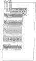
Figure 18 represents the exciter comb with 8 teeth;
Figure 19 represents the sectional view of exciter comb shown in Figure 180 along F-F;
Figure 20 represents the outer rim output on every side of comb shown in Figure 180;
Figure 21 represents another embodiment of pectination exciter;
Figure 22 represents the part of pectinate texture and electrode input.
Accompanying drawing describes in detail
Fig. 1 is the schematic diagram with the 1 2D exciter of representing.This exciter is actually a cylindric piezoelectric actuator with square sectional, an axial core 4 is arranged in this embodiment to hold an elongated elements 5, as optical fiber.Electrode is arranged in the piezoelectric material body in four zones that separate, and wherein four zones that separate are represented with upper and lower a, left side and the right side.Each group of these electrodes can encourage individually; For example, if only encourage top, then the top of exciter will be shunk, so exciter will bend towards constriction, and wherein this constriction will move the elongated elements of working with piezoelectric actuator.Electrode by correspond respectively to, left and right and under input U, L, R and D encourage.For effectively utilize exciter mainly on the Z direction, to extend and thereby only occupy this fact of the X and the Y direction confined space, the electrode input can all be positioned at the same side of exciter.
Each electrode is preferably on the whole length of exciter and extends.But also can only encourage the part of exciter.
Fig. 2 is the cross-sectional view of certain preferred integrated piezoelectric ceramic block, will explain its manufacture method in detail in the next stage of this specification,
Have the A and the B electrode layer of crossover towards the top of exciter structure, this structure is extended on the whole width of piece.Similarly, the E and the B electrode layer that have crossover towards the bottom of exciter structure.All B layers are ground connection easily, and A or E are applied voltage with the motion that causes respectively up or down.Under this scheme, driving voltage is a unipolar voltage, and the polarization direction is parallel to the battery orientation that applies, and makes piezoelectric work with collapsed mode.
Zone line at piece is the C and the D electrode layer of crossover.The whole width of D layer extend through piece, and the C electrode is divided into left and right sides two parts.Suitably will produce left and right sides deflection to C group electrode application voltage.
The specific dimensions of present embodiment piezoelectric actuator writes among Fig. 2.The thickness measurement of soft PZT material layer is 22.5 μ m, and the thickness of electrode itself is 2.5 μ m.Core accounts for the thickness 200 μ m of electrode so that hold the square central core of 160 μ m.The center clearance of an about 0.2mm is set between the bias electrode of the left and right sides.
Fig. 3 represents another embodiment of 2D piezoelectric actuator.This piezoelectric actuator comprises one and aforementioned similar crossover electrode shown in Figure 2.This type of piezoelectric actuator has been abolished central core, thus can be in piezoelectric ceramic distribution electrode more effectively.This type of specific piezoelectric actuator is the piece of a 1.8 * 1.8mm, though not shown, have the effective length of 31mm and the total length of 41mm.Have 54 layers of soft PZT material that is separated the 30 μ m of 2.5 μ m by electrode equally.Electric capacity for (U/D) is 0.3 μ F, is 0.7 μ F for the electric capacity of (L/R).Each electrode of this structure has the length of width and the 31mm of 1.6mm, extends along its length in parallel with each other simultaneously.The center clearance of L/R bias electrode is 0.2mm.And operating voltage is+90V ,-15V, and bias voltage+/-37.5V and driving voltage+/-52.5V.If piezoelectric actuator is not loaded, then when an end clamp down on approximately+/-during 0.8N, for being deflected to+/-125 μ m of U/D and L/R.
Above-mentioned 2D exciter can be the unit that isolates, or the part of toothed exciter comb, and each broach has the electrode structure of the above-mentioned type.
In order to make the piezoelectric ceramic comb, piezoceramic material such as germanium lead titanates become layered arrangement with battery lead plate.Just as already discussed, when battery lead plate when applying voltage drive, piezoceramic material can shrink or sprawl uniformly as described above, this will depend on the voltage that is applied.In these cases, voltage is only in the scope of 0V-90V, and is and therefore always positive, therefore will cause piezoceramic material to shrink.By the different piece of systolic pressure electroceramics material, in whole piezoelectric actuator, produce different effects.
A kind of particularly advantageous method of making 2D exciter group is that they are manufactured the pectination form that has controlled separately sawtooth.The method for optimizing of making this pectination exciter is by the layered electrode plate of making the whole area size of exciter in a very big rectangular shape, and cuts in position to obtain pectination again and carry out.
Plate shown in Fig. 4,5,6,7 and 8 is marked with D, C, B, A and E respectively, and as illustrated in fig. 9 in the top of each other layered arrangement.Fig. 9 represents the hole 32 of having cut, and the cycle in hole is a layered electrode, and this layer is the thick pottery of 22.5 μ m that is between each 2.5 μ m layer of electrode.
Though 5 different plates are arranged, plates dissimilar in 3 are arranged.As can be seen, the similar part of plate D and B is that they all have an input (in Figure 10 and 12 as seen) for each last sawtooth, and therefore each sawtooth can encourage independently from Fig. 4 and Fig. 6.
Fig. 7 and plate A and E shown in Figure 8 have only an electrode input, and all A of final sawtooth and/or the E electrode is simultaneously non-is energized independently.In Figure 13 and 14, can see otch.The input layout of B is different from the input layout of D; The input layout of A and E is also different.
Electrode of third kind plate as shown in Figure 5.When the finger electrode 70 (as shown in figure 11) of plate C cut downwards from the centre, saw kerf also arrived the bottom of electrode material fully.
When electric current passed through, if see sawtooth comb and sawtooth array from left to right from the end that optical fiber stretches out, the D plate produced the side-to-side movement of exciter sawtooth.C plate conduction left and right sides bias voltage is with the voltage in the balance D plate.As can be seen, this special case has 8 sawtooth combs, because 8 intervals are arranged between the electrode in the C plate.The B plate is similar to the D plate, but its location makes its voltage cause the exciter sawtooth to move up and down.A plate and E plate are the positive and negative plate bias voltages that moves up and down that is respectively applied for the exciter sawtooth.
The layout of Fig. 9 display plate is: ABABACDCDCDCD hole 42DCDCDCDCABABA.
Also can adopt other structure.
Figure 10,11,12,13 and 14 is illustrated in the plate position of the sawtooth otch of the sawtooth that 8 (in these examples) producing the exciter comb separate.Sawtooth otch in the plate make in each exciter comb plate structure as shown in figure 15.Each otch 0.2mm is wide, and all the other 0.8mm of exciter are the width of each sawtooth.
Every class plate that Figure 16 sees separately after representing to be cut.The combination of all these stratiform septums and piezoelectric will be formed a sawtooth of exciter comb.
How each other Figure 17 represents plates different in exciter comb electrical ties.Not shown in the figures portalling; The hole can be bored later on.Each sawtooth has 4 electrode inputs; U/D control, L/R control ,+bias voltage and-bias voltage.
Figure 18 represents the pectination exciter structure of 8 sawtooth, has 2 points and F on it.
Figure 19 represents the F-F sectional view along Figure 43.The bottom of comb is wide to be 1mm, and notch portion is 0.8mm.This figure represents the side length of each sawtooth.
Figure 20 represents the inlet point of all electrode inputs.U/D1~U/D8 respectively on 8 exciter teeth/following input.For the mark of a left side/right side (L/R) electrode input similarly.+ and-be the bias voltage input; Press input to have 8 inputs, each input to be used for/input of following positive and negative bias voltage for a left side/right avertence.As can be seen from Figure 20, all electrode input all is in the side of comb.This is for the ease of operating and make the more compact structure of whole comb.
Figure 21 represents another embodiment of the integrated piezoelectric exciter 30 that cuts, and wherein cutting mode is to be similar to 32 sawtooth combs; Each sawtooth 20 is used as an independently piezoelectric actuator.Each sawtooth 20 of piezoelectric ceramic comb 30 has a hole that therefrom gets out, and optical fiber can therefrom pass.This type of comb can be piled up at an easy rate to form the comb array, can be used for the input array or the output array of optical system.For example, 32 combs of 32 exciter sawtooth can be made the individual switch of 1024 * 1024 (i.e. 1024 mouths) thus in the face of 32 combs of 32 sawtooth.
Figure 22 represents to have the pectinate texture of some electrode inputs.The electrode excitation thing input 70 of each broach 20 is divided into 4.Can see that from the example of 2 sawtooth shown in Figure 22 the input connect mechanism is arranged to make electrode input D, R, L and U separately to appear at around the outward flange of comb.Can pile up many exciter combs with form arranged side by side in such a way, and all electrode inputs are easy to still use.
Claims (7)
1. integral type exciter, this exciter is fixed on the supporting construction and in the Z direction and extends along length, and have one movably terminal, described exciter comprises the lamination that a battery lead plate and piezoelectric interweave; And this exciter has first electrode layer; Encourage the device of described first electrode layer, thereby carry out terminal deflection in a direction, this direction is generally first Y direction; And the second electrode lay; Encourage the device of described the second electrode lay, thereby carry out terminal deflection in a direction, this direction is generally directions X; It is characterized in that each of exciter layer extended usually on the Z direction, and exciter comprises the third electrode layer, this third electrode layer and described first electrode layer separate along the Y direction; With the device of the described third electrode layer of excitation, thereby carry out terminal deflection in a direction, this direction is generally second Y direction.
2. exciter as claimed in claim 1 is characterized in that exciter does not comprise centre bore.
3. the described exciter of arbitrary as described above claim is characterized in that described the second electrode lay is clipped between first electrode layer and the third electrode layer.
4. exciter as claimed in claim 1 or 2 is characterized in that the battery lead plate of described the second electrode lay comprises first's electrode layer and second portion electrode layer, and first's electrode layer separates at directions X and second portion electrode layer in fact; Described first electrode layer has provides first device that encourages bias voltage to carry out deflection at first directions X, and described second portion electrode layer has provides the second excitation bias voltage to carry out deflection at second directions X.
5. exciter as claimed in claim 4, thus also comprise in fact extend through first electrode layer and second portion electrode layer and first's electrode layer and the interactional battery lead plate of second portion electrode layer.
6. exciter as claimed in claim 1 or 2 is characterized in that exciter is a kind of common cylindric.
7. exciter as claimed in claim 1 is characterized in that exciter comprises one or more passages that extend along the Z direction on length; Hold one or more microscler elements whereby.
Applications Claiming Priority (10)
| Application Number | Priority Date | Filing Date | Title |
|---|---|---|---|
| GB0115068.9 | 2001-06-20 | ||
| GBGB0115068.9A GB0115068D0 (en) | 2000-11-13 | 2001-06-20 | Multiport optical switch |
| GBGB0115067.1A GB0115067D0 (en) | 2000-11-13 | 2001-06-20 | Optical switching assembly |
| GB0115067.1 | 2001-06-20 | ||
| GB0116245A GB0116245D0 (en) | 2001-07-05 | 2001-07-05 | Multiport optical switching assembly |
| GB0116245.2 | 2001-07-05 | ||
| PCT/GB2001/005361 WO2002046825A1 (en) | 2000-12-04 | 2001-12-04 | Beam steering arrangements and optical switches |
| GBPCT/GB01/05361 | 2001-12-04 | ||
| GB0213020.1 | 2002-06-06 | ||
| GB0213020A GB2378573B (en) | 2001-06-20 | 2002-06-06 | A piezoelectric actuator |
Publications (2)
| Publication Number | Publication Date |
|---|---|
| CN1547779A CN1547779A (en) | 2004-11-17 |
| CN100524869C true CN100524869C (en) | 2009-08-05 |
Family
ID=27447956
Family Applications (1)
| Application Number | Title | Priority Date | Filing Date |
|---|---|---|---|
| CNB02812202XA Expired - Lifetime CN100524869C (en) | 2001-06-20 | 2002-06-19 | Beam steering arrangements and optical switches |
Country Status (11)
| Country | Link |
|---|---|
| US (1) | US7026745B2 (en) |
| EP (1) | EP1402582B1 (en) |
| JP (1) | JP4240472B2 (en) |
| CN (1) | CN100524869C (en) |
| AT (1) | ATE387725T1 (en) |
| CA (1) | CA2450613C (en) |
| DE (1) | DE60225281T2 (en) |
| ES (1) | ES2302812T3 (en) |
| GB (1) | GB2378573B (en) |
| IL (1) | IL159322A0 (en) |
| WO (1) | WO2002103816A2 (en) |
Families Citing this family (12)
| Publication number | Priority date | Publication date | Assignee | Title |
|---|---|---|---|---|
| WO2005119313A2 (en) | 2004-05-29 | 2005-12-15 | Polatis Ltd | Optical switches & actuators |
| US20080131048A1 (en) * | 2004-08-24 | 2008-06-05 | Auckland Uniservices Limited | Optical Fibre Switch |
| GB2423788A (en) * | 2005-03-02 | 2006-09-06 | Pbt | Piezo ceramic actuator for a lock bolt |
| KR20100097112A (en) * | 2007-11-21 | 2010-09-02 | 코니카 미놀타 옵토 인코포레이티드 | Piezoelectric actuator, driving device, positioning device, and laser module |
| US7786648B2 (en) * | 2008-08-18 | 2010-08-31 | New Scale Technologies | Semi-resonant driving systems and methods thereof |
| US8217553B2 (en) * | 2008-08-18 | 2012-07-10 | New Scale Technologies | Reduced-voltage, linear motor systems and methods thereof |
| WO2014005949A1 (en) | 2012-07-05 | 2014-01-09 | Noliac A/S | A wobble motor with a solid state actuator |
| GB2531552B (en) * | 2014-10-21 | 2017-12-27 | Polatis Ltd | Crosstalk reduction technique for multi-channel driver circuits |
| JP2022548258A (en) * | 2019-09-12 | 2022-11-17 | テクニーシェ・ユニバーシタイト・アイントホーベン | Apparatus Arranged for Aligning Optical Components to On-Chip Ports, and Corresponding Systems and Methods |
| CN115039243A (en) | 2020-02-07 | 2022-09-09 | 京瓷株式会社 | Piezoelectric element |
| US20230320220A1 (en) * | 2020-07-03 | 2023-10-05 | Kyocera Corporation | Piezoelectric element |
| US20230397499A1 (en) | 2020-10-23 | 2023-12-07 | Kyocera Corporation | Piezoelectric actuator |
Family Cites Families (10)
| Publication number | Priority date | Publication date | Assignee | Title |
|---|---|---|---|---|
| US4812697A (en) * | 1986-04-09 | 1989-03-14 | Taga Electric Co., Ltd. | Ultrasonic vibrator and a method of controllingly driving same |
| US4958100A (en) * | 1989-02-22 | 1990-09-18 | Massachusetts Institute Of Technology | Actuated truss system |
| US5027028A (en) * | 1989-08-29 | 1991-06-25 | Skipper John D | Piezoelectric motor |
| US5081391A (en) * | 1989-09-13 | 1992-01-14 | Southwest Research Institute | Piezoelectric cylindrical transducer for producing or detecting asymmetrical vibrations |
| JPH03117384A (en) * | 1989-09-28 | 1991-05-20 | Canon Inc | Friction material for ultrasonic motor |
| US5345137A (en) * | 1991-04-08 | 1994-09-06 | Olympus Optical Co., Ltd. | Two-dimensionally driving ultrasonic motor |
| JPH08111991A (en) * | 1994-08-19 | 1996-04-30 | Mitsui Petrochem Ind Ltd | Piezoelectric vibrator for ultrasonic motor and method for fitting it |
| JP2799410B2 (en) | 1995-02-02 | 1998-09-17 | サンケン電気株式会社 | DC converter device |
| DE19605214A1 (en) * | 1995-02-23 | 1996-08-29 | Bosch Gmbh Robert | Ultrasonic drive element |
| US6359370B1 (en) * | 1995-02-28 | 2002-03-19 | New Jersey Institute Of Technology | Piezoelectric multiple degree of freedom actuator |
-
2002
- 2002-06-06 GB GB0213020A patent/GB2378573B/en not_active Expired - Lifetime
- 2002-06-19 WO PCT/GB2002/002826 patent/WO2002103816A2/en active IP Right Grant
- 2002-06-19 ES ES02735631T patent/ES2302812T3/en not_active Expired - Lifetime
- 2002-06-19 US US10/480,519 patent/US7026745B2/en not_active Expired - Lifetime
- 2002-06-19 EP EP02735631A patent/EP1402582B1/en not_active Expired - Lifetime
- 2002-06-19 JP JP2003506021A patent/JP4240472B2/en not_active Expired - Lifetime
- 2002-06-19 CA CA2450613A patent/CA2450613C/en not_active Expired - Lifetime
- 2002-06-19 IL IL15932202A patent/IL159322A0/en unknown
- 2002-06-19 DE DE60225281T patent/DE60225281T2/en not_active Expired - Lifetime
- 2002-06-19 CN CNB02812202XA patent/CN100524869C/en not_active Expired - Lifetime
- 2002-06-19 AT AT02735631T patent/ATE387725T1/en not_active IP Right Cessation
Also Published As
| Publication number | Publication date |
|---|---|
| EP1402582B1 (en) | 2008-02-27 |
| EP1402582A2 (en) | 2004-03-31 |
| CN1547779A (en) | 2004-11-17 |
| US7026745B2 (en) | 2006-04-11 |
| DE60225281D1 (en) | 2008-04-10 |
| ES2302812T3 (en) | 2008-08-01 |
| WO2002103816A3 (en) | 2003-06-19 |
| CA2450613C (en) | 2010-12-07 |
| GB0213020D0 (en) | 2002-07-17 |
| US20040251771A1 (en) | 2004-12-16 |
| GB2378573A (en) | 2003-02-12 |
| WO2002103816A2 (en) | 2002-12-27 |
| JP2004531189A (en) | 2004-10-07 |
| CA2450613A1 (en) | 2002-12-27 |
| IL159322A0 (en) | 2004-06-01 |
| DE60225281T2 (en) | 2009-03-05 |
| JP4240472B2 (en) | 2009-03-18 |
| GB2378573B (en) | 2003-09-10 |
| ATE387725T1 (en) | 2008-03-15 |
Similar Documents
| Publication | Publication Date | Title |
|---|---|---|
| CN100524869C (en) | Beam steering arrangements and optical switches | |
| US5852337A (en) | Piezoelectric film-type element | |
| JP4289511B2 (en) | Piezoelectric actuator | |
| US6066911A (en) | Ultrasonic driving element | |
| JP2001518721A (en) | Piezoelectric element | |
| CN102185096A (en) | Piezoelectric actuator and linear piezoelectric motor | |
| EP2937913A1 (en) | Piezoelectric actuator for an ultrasonic motor | |
| JPH07193292A (en) | Twist actuator and its manufacture | |
| JP4699826B2 (en) | One-dimensional piezoelectric actuator array | |
| JP4106378B2 (en) | Piezoelectric actuator | |
| EP0897802A3 (en) | Ink-jet head and methods of manufacturing and driving the same | |
| JP4447250B2 (en) | Piezoelectric actuator array and manufacturing method | |
| AU2002218625A1 (en) | Double electromechanical element | |
| US20090243437A1 (en) | Multilayered actuators having interdigital electrodes | |
| JPH0394487A (en) | Piezoelectric actuator | |
| JPH03183371A (en) | Multilayer piezoelectric actuator | |
| JP5561247B2 (en) | Piezoelectric element | |
| JP2015087548A (en) | Piezoelectric actuator | |
| JPS63288075A (en) | Electrostrictive effect element | |
| JPH0770760B2 (en) | Multilayer piezoelectric actuator element | |
| JP5144097B2 (en) | Ultrasonic motor device | |
| JPS61183981A (en) | Piezoelectric displacement device | |
| CN101471613B (en) | Piezoelectric clamping device | |
| JPH0373467B2 (en) | ||
| JP2005026583A (en) | Ceramic laminated electromechanical sensing element |
Legal Events
| Date | Code | Title | Description |
|---|---|---|---|
| C06 | Publication | ||
| PB01 | Publication | ||
| C10 | Entry into substantive examination | ||
| SE01 | Entry into force of request for substantive examination | ||
| C14 | Grant of patent or utility model | ||
| GR01 | Patent grant | ||
| CX01 | Expiry of patent term |
Granted publication date: 20090805 |
|
| CX01 | Expiry of patent term |