CN100524954C - High-density connector assembly with tracking ground structure - Google Patents
High-density connector assembly with tracking ground structure Download PDFInfo
- Publication number
- CN100524954C CN100524954C CNB2003801090128A CN200380109012A CN100524954C CN 100524954 C CN100524954 C CN 100524954C CN B2003801090128 A CNB2003801090128 A CN B2003801090128A CN 200380109012 A CN200380109012 A CN 200380109012A CN 100524954 C CN100524954 C CN 100524954C
- Authority
- CN
- China
- Prior art keywords
- terminal
- connector
- signal
- signal terminal
- centre
- Prior art date
- Legal status (The legal status is an assumption and is not a legal conclusion. Google has not performed a legal analysis and makes no representation as to the accuracy of the status listed.)
- Expired - Fee Related
Links
Images


Classifications
-
- H—ELECTRICITY
- H01—ELECTRIC ELEMENTS
- H01R—ELECTRICALLY-CONDUCTIVE CONNECTIONS; STRUCTURAL ASSOCIATIONS OF A PLURALITY OF MUTUALLY-INSULATED ELECTRICAL CONNECTING ELEMENTS; COUPLING DEVICES; CURRENT COLLECTORS
- H01R13/00—Details of coupling devices of the kinds covered by groups H01R12/70 or H01R24/00 - H01R33/00
- H01R13/46—Bases; Cases
- H01R13/516—Means for holding or embracing insulating body, e.g. casing, hoods
- H01R13/518—Means for holding or embracing insulating body, e.g. casing, hoods for holding or embracing several coupling parts, e.g. frames
-
- H—ELECTRICITY
- H01—ELECTRIC ELEMENTS
- H01R—ELECTRICALLY-CONDUCTIVE CONNECTIONS; STRUCTURAL ASSOCIATIONS OF A PLURALITY OF MUTUALLY-INSULATED ELECTRICAL CONNECTING ELEMENTS; COUPLING DEVICES; CURRENT COLLECTORS
- H01R12/00—Structural associations of a plurality of mutually-insulated electrical connecting elements, specially adapted for printed circuits, e.g. printed circuit boards [PCB], flat or ribbon cables, or like generally planar structures, e.g. terminal strips, terminal blocks; Coupling devices specially adapted for printed circuits, flat or ribbon cables, or like generally planar structures; Terminals specially adapted for contact with, or insertion into, printed circuits, flat or ribbon cables, or like generally planar structures
- H01R12/70—Coupling devices
- H01R12/71—Coupling devices for rigid printing circuits or like structures
- H01R12/72—Coupling devices for rigid printing circuits or like structures coupling with the edge of the rigid printed circuits or like structures
- H01R12/722—Coupling devices for rigid printing circuits or like structures coupling with the edge of the rigid printed circuits or like structures coupling devices mounted on the edge of the printed circuits
- H01R12/727—Coupling devices presenting arrays of contacts
-
- H—ELECTRICITY
- H01—ELECTRIC ELEMENTS
- H01R—ELECTRICALLY-CONDUCTIVE CONNECTIONS; STRUCTURAL ASSOCIATIONS OF A PLURALITY OF MUTUALLY-INSULATED ELECTRICAL CONNECTING ELEMENTS; COUPLING DEVICES; CURRENT COLLECTORS
- H01R13/00—Details of coupling devices of the kinds covered by groups H01R12/70 or H01R24/00 - H01R33/00
- H01R13/46—Bases; Cases
- H01R13/514—Bases; Cases composed as a modular blocks or assembly, i.e. composed of co-operating parts provided with contact members or holding contact members between them
-
- H—ELECTRICITY
- H01—ELECTRIC ELEMENTS
- H01R—ELECTRICALLY-CONDUCTIVE CONNECTIONS; STRUCTURAL ASSOCIATIONS OF A PLURALITY OF MUTUALLY-INSULATED ELECTRICAL CONNECTING ELEMENTS; COUPLING DEVICES; CURRENT COLLECTORS
- H01R13/00—Details of coupling devices of the kinds covered by groups H01R12/70 or H01R24/00 - H01R33/00
- H01R13/62—Means for facilitating engagement or disengagement of coupling parts or for holding them in engagement
- H01R13/629—Additional means for facilitating engagement or disengagement of coupling parts, e.g. aligning or guiding means, levers, gas pressure electrical locking indicators, manufacturing tolerances
- H01R13/631—Additional means for facilitating engagement or disengagement of coupling parts, e.g. aligning or guiding means, levers, gas pressure electrical locking indicators, manufacturing tolerances for engagement only
- H01R13/6315—Additional means for facilitating engagement or disengagement of coupling parts, e.g. aligning or guiding means, levers, gas pressure electrical locking indicators, manufacturing tolerances for engagement only allowing relative movement between coupling parts, e.g. floating connection
-
- H—ELECTRICITY
- H01—ELECTRIC ELEMENTS
- H01R—ELECTRICALLY-CONDUCTIVE CONNECTIONS; STRUCTURAL ASSOCIATIONS OF A PLURALITY OF MUTUALLY-INSULATED ELECTRICAL CONNECTING ELEMENTS; COUPLING DEVICES; CURRENT COLLECTORS
- H01R13/00—Details of coupling devices of the kinds covered by groups H01R12/70 or H01R24/00 - H01R33/00
- H01R13/646—Details of coupling devices of the kinds covered by groups H01R12/70 or H01R24/00 - H01R33/00 specially adapted for high-frequency, e.g. structures providing an impedance match or phase match
- H01R13/6461—Means for preventing cross-talk
- H01R13/6471—Means for preventing cross-talk by special arrangement of ground and signal conductors, e.g. GSGS [Ground-Signal-Ground-Signal]
-
- H—ELECTRICITY
- H01—ELECTRIC ELEMENTS
- H01R—ELECTRICALLY-CONDUCTIVE CONNECTIONS; STRUCTURAL ASSOCIATIONS OF A PLURALITY OF MUTUALLY-INSULATED ELECTRICAL CONNECTING ELEMENTS; COUPLING DEVICES; CURRENT COLLECTORS
- H01R13/00—Details of coupling devices of the kinds covered by groups H01R12/70 or H01R24/00 - H01R33/00
- H01R13/648—Protective earth or shield arrangements on coupling devices, e.g. anti-static shielding
- H01R13/658—High frequency shielding arrangements, e.g. against EMI [Electro-Magnetic Interference] or EMP [Electro-Magnetic Pulse]
- H01R13/6581—Shield structure
- H01R13/6585—Shielding material individually surrounding or interposed between mutually spaced contacts
- H01R13/6586—Shielding material individually surrounding or interposed between mutually spaced contacts for separating multiple connector modules
- H01R13/6587—Shielding material individually surrounding or interposed between mutually spaced contacts for separating multiple connector modules for mounting on PCBs
-
- H—ELECTRICITY
- H01—ELECTRIC ELEMENTS
- H01R—ELECTRICALLY-CONDUCTIVE CONNECTIONS; STRUCTURAL ASSOCIATIONS OF A PLURALITY OF MUTUALLY-INSULATED ELECTRICAL CONNECTING ELEMENTS; COUPLING DEVICES; CURRENT COLLECTORS
- H01R13/00—Details of coupling devices of the kinds covered by groups H01R12/70 or H01R24/00 - H01R33/00
- H01R13/648—Protective earth or shield arrangements on coupling devices, e.g. anti-static shielding
- H01R13/658—High frequency shielding arrangements, e.g. against EMI [Electro-Magnetic Interference] or EMP [Electro-Magnetic Pulse]
- H01R13/6598—Shield material
- H01R13/6599—Dielectric material made conductive, e.g. plastic material coated with metal
Abstract
A connector assembly is suitable for connecting circuit boards together. The connector assembly includes a series of ground and signal terminal sets assembled in terminal assemblies held within a housing. The ground terminals sets include a set of flat contact blades that are aligned together in abutting contact to form a line of ground contacts blades and the signal terminals are arranged in sets on opposite sides of the ground terminal contact blades. The signal terminals have general L-shapes that are arranged in sets of two pairs of contacts to form a cruciform pattern with an associated ground contact blade in the midst of the pattern of four. The terminal assemblies are formed from housings that have interfitting projections on their exterior sides, and the ground terminal housing is plated with a conductive material. This effectively surrounds each signal terminal in its extent through the signal terminal housing.
Description
Technical field
The present invention relates to high-density connector, more particularly, relate to and be used for high-density connector that two printed circuit board (PCB)s are linked together with the form of orthogonal arrangement.
Background technology
The high density connected system is used for various data communication applications, and wherein a kind of this application is the webserver and router.In many application, the system of connecting comprises the plug and socket connector that is installed on the various boards, and for example with the rigging-angle connector form of routine, wherein two circuit boards relatively are orientated to 90 ° mutually, so that the edge of two circuit boards adjoins each other.High-density connector uses latch and boxlike terminal or slide plate (blade) to the slide terminal fit structure usually.Use these high density structures, be desirable to provide the shielding of signal terminal completely from the bonder terminal afterbody to the bonder terminal contact portion.
In the high-density connector that utilizes the sheet type structure, extend through at terminal under the situation of thin slice main body, or at terminal by under the situation in the path of the installation end of the connector assembly abutting end on to it, no matter this terminal scheduled transmission mono signal or differential signal all are difficult to provide sufficient shielding to signal terminal.Knew already, prior art is passed through to intersect plate in the front portion utilization that cooperates the district, and the complicated shielding part of formation provides shielding in some cases, and this shielding part has to this locates crooked rectangular part, it extends outside the plane of earthing member, so that one or more shielding walls to be provided.Electricity isolation signals terminal comprises the earth shield that is provided with near signal terminal, increases connector like this and forms thin slice, or the structural complexity of terminal assemblies.Be not always can be in structure crooked and form metal shielding board so that fully relevant signal terminal is enclosed in this thin slice.If signal terminal is surrounded in shielding, so can minimum crosstalk and the situation of electrical noise under obtain high signaling rate.
The high density interconnect welding system that therefore need in whole connector, have signal terminal shielding more completely.
Summary of the invention
The present invention relates to overcome the improved high density interconnect connected components of aforesaid drawbacks.
Therefore, general purpose of the present invention provides connector assembly, wherein one of connector constitutes with a plurality of independent terminal subassemblies at least, preferably, use the sheet form of being arranged to over-over mode about this bonder terminal, make each earthing member join by relevant signal thin slice and its opposite side side.
Another object of the present invention provides the high-density connector assembly that is used for high-speed applications, this connector assembly is assembled with a plurality of terminal assemblies, each terminal assemblies comprises first group of signal terminal, second group of signal terminal and relative winding ground terminal, this first and second signal terminal set is supported by insulation shell, this ground terminal set is relevant with ground structure, this ground structure comprises the supportive body that is formed with a plurality of passages thereon, this supportive body has formation a plurality of signal terminals thereon and admits groove, and this supportive body uses the electric conducting material such as the coat of metal or coating to cover, thereby supportive body provides shielding to the ground structure in whole terminal assemblies.
Another purpose of the present invention provides the head assembly that is used for high-speed applications, this head assembly comprises having the head pedestal that at least one is formed on hollow socket (receptacle) wherein, a plurality of terminal assemblies, each comprises a plurality of signal terminals and earth terminal by the setting of earth terminal-signal terminal-earth terminal order this terminal assemblies, some terminal group are signal terminals and are supported by insulating body, this insulating body is joined by the ground terminal set side, as its relevant terminal, every winding ground terminal comprise elongated base part and a plurality of contact portion and on its opposite side from a plurality of afterbodys of its extension.
Another object of the present invention provides high-density connector, it has a plurality of conducting terminals that are supported on the insulation shell, wherein this terminal is separated into the signal terminal set and the ground terminal set of different in kind, this earth terminal has dual flat slide plate form, this flat slide plate stretches out forward from connector body, and signal terminal has roughly L shaped contact portion, and this signal terminal is arranged on the opposite side of this ground connection slide plate with the cross form.
Another purpose of the present invention provides and is used for the connector that matches with above-mentioned high-density connector, wherein the signal terminal of this connector comprises contact portion, it also is L shaped and comprises a pair of contact arm that this contact arm stretches out in different planes from the L shaped main part of this terminal.
A further object of the present invention provides high density, high speed connector structure, and it utilizes dual ground connection, and it provides the ground connection reference and isolation is provided between signal terminal is capable signal terminal.
Another object of the present invention provides high density, high speed connector, it is suitable for two circuit board interconnects together, this connector comprises the terminal assemblies group that remains on the different in kind in the housing, this terminal assemblies comprises a plurality of afterbodys that are used for this terminal is connected in circuit board, with be used for and the contacted a plurality of contact portions of the terminal of the connector that matches, the terminal group of each different in kind comprises the centre-point earth structure of the centre-point earth plate with conduction, the centre-point earth plate of this conduction has a plurality of contact portions from its extension, this centre-point earth plate is sealed in the dielectric enclosure, this shell has setting conductive coating on its outer surface, this outer surface contacts with the centre-point earth plate, the terminal group of each different in kind also comprises a plurality of signal terminals of being arranged to two arrays, each signal terminal comprises afterbody that is used for the connecting circuit plate and the contact portion that is used to contact the connector that matches, and with connect together main part of this signal terminal afterbody and contact portion, each signal array is maintained in the dielectric enclosure, this signal terminal shell is arranged on the opposite side of ground structure, each signal terminal shell comprises the platform of a plurality of projectioies that seal this signal terminal main body, and the centre-point earth structure comprises a plurality of passages, each passage is admitted a boss on the relative signal terminal shell, this terminal assemblies also comprise on the outer surface that is arranged on this signal terminal shell and with this centre-point earth structure and the isolated a pair of ground plate of signal terminal, thereby each signal terminal main body by the reference grounded part be enclosed in.
The present invention realizes aforementioned and other purposes by its novel particular structure.In this respect, the head of connector assembly partly comprises the insulating body with a plurality of sidewalls, and this sidewall forms one or more hollow sockets.Array of conductive terminals remains in this head socket, and a plurality of array is arranged to form the single-end sub-component.Each this assembly preferably include have pedestal with a plurality of centre-point earth spares that contact slide plate of isolated order from its extension.This contact slide plate is joined by a pair of signal terminal set side, each terminal group comprise insulating base with from its extension and be positioned at a plurality of contact portions that contact the slide plate side.Additional ground terminal set is arranged on the opposite side of one of this signal terminal set, and this ground terminal set also has base part, and this base part has a plurality of contact slide plates from its extension.
The terminal assemblies of these socket connectors has a plurality of afterbodys disposed thereon, and these afterbodys can be taked forms such as mounted on surface afterbody, soldered ball afterbody, submissive latch.Signal terminal is preferably formed and is L shaped contact portion, and four this contact portions are positioned at the side of each ground connection contact slide plate, this terminal group is arranged to a kind of form in each this head socket, so that their order with signal terminal-earth terminal-signal terminal in each terminal assemblies form rows of terminals, and final ground terminal set is assembled into this group terminal finishes this terminal with earth terminal whole order.By this way, whole bottom section terminal group is formed by these terminal row that are so arranged, so that four signal terminals form the cross figure around each relevant ground connection contact slide plate.
The relative pin connector of connector assembly of the present invention has a plurality of terminal assemblies that remain in the housing.Each terminal assemblies is configured to so that it can individually insert in this housing or from this housing pulls down, and can repair or change each terminal assemblies rather than change the whole plug connector.Each terminal assemblies is made of a plurality of array of terminals, and some arrays are installed on the insulator, preferably adopts the form of thin slice or shell.Each this terminal assemblies preferably includes a pair of insulation signal terminal shell, each terminal shell supports a plurality of electrically conductive signal terminals, specifically, the part and the terminal bodies part of afterbody are touched in support and connection, this connect contact portion and afterbody from the signal terminal shell along its not ipsilateral stretch out.
The contact portion of this signal terminal each have a pair ofly by the interconnective contact arm of pedestal, and this contact arm forms L shaped orientation, and it is sliding engaged to the L shaped contact portion of this head connector.This juncture can be with four corner signalization terminals around the box of the imagination of each centre-point earth contact slide plate setting-out.
Each also comprises the centre-point earth structure that supports ground plate this terminal assemblies, and this ground plate has a plurality of earth terminals, and this earth terminal has the afterbody and the contact portion of extending from the flat body of this ground plate.The contact portion of each earth terminal comprises a pair of contact arm.By this way, the ground connection contact portion of head connector and pin connector will laterally be bonded with each other, and take to extend through the criss-cross form of ground connection in the cooperation district of two connectors.Therefore, in the cooperation district of two connectors, the cross figure is formed between the ground connection contact slide plate of joint.
In an importance of the present invention, the terminal assemblies of pin connector comprises one or more dielectric inserts that apply in its outer surface conduction.These inserts are preferably taked the form of the shell of mounting terminal.Each sort signal terminal shell has the platform of a plurality of passages and rising thereon, and each platform surrounds the individual signals terminal thereon, normally surrounds its main part.Conductive coating can be disposed thereon, to form the shielding that partly centers on this signal terminal.
In a preferred embodiment of the invention, the centre-point earth structure comprises the dielectric enclosure that partly centers on this centre-point earth plate, and the contact portion of this centre-point earth plate and afterbody are exposed.The outer surface of this electrolyte shell applies with electric conducting material, and for example metal plating, and this coating contact centre-point earth plate make whole ground structure electrically work, in this embodiment as single earthing member.The electrolyte shell of electroplating has formation a plurality of passages thereon, and these passages are formed by the platform of isolated rising.The platform of the rising of signal terminal shell is received within the passage of the centre-point earth structure on the relative side of this centre-point earth structure, to form the terminal assemblies of sandwich type or stratification.Two other ground terminal array also are arranged to for the ground connection reference is provided on the outside of two signal terminal shells.These two other ground terminal array are preferably taked to have from the form of the integral slab of the afterbody of its extension and contact portion, and they are used for separating the passage of admitting individual signals terminal each conduction therein.By this way, each signal terminal is surrounded fully by four grounded wall, so that itself and other each signal terminal electricity is isolated, and feasible the crosstalking and the electrical noise minimum of taking place of this structure.
This respect of the present invention and other main aspect, socket connector comprises a plurality of terminal subassemblies, these terminal subassemblies are assembled by different parts at least, preferably are assembled by four different parts.These parts comprise two signal terminal set that are positioned at centre-point earth terminal group side, and other ground terminal set preferably is arranged to so that these terminal group can be arranged to the order of ground terminal set-signal terminal set-ground terminal set.Single ground terminal set can make this whole assembly keep the order of ground connection-signal-ground connection as the end of this assembly.This signal terminal set is supported on the dielectric housing, and have from a side of this housing and extend the afterbody that matches with circuit board, be used for the contact portion that cooperates with opposing connector from this housing opposite side extension, and the main part that this contact portion and afterbody are linked together, this main part is by this housings support.
For the connector to this assembly provides effective shielding, and of the present invention another main aspect, the inner part of each shell comprises the shielding of ground connection, and the shielding of this ground connection can remain in plastics or the dielectric support, and can form a plurality of contact slide plates within it.These first and second groups of signals and earth terminal have the flat slide plate part that is arranged in each connector component, make first and second windings ground terminal preferably adjoin each other and along the downward straight-line extension in the center of this thin slice, and first and second groups of signal terminals are positioned at the opposite side of this first and second windings ground terminal, or be positioned at its side, the insulating cover of described first and second groups of signal terminals prevents that between signal terminal and earth terminal accidental short circuit takes place.These first and second groups of signal terminals also are arranged to so that a pair of first signal terminal and a pair of secondary signal terminal are arranged on the opposite side of one of contact portion of this first and second windings ground terminal.In this set, L shaped signal terminal contact portion is along being parallel to and extending perpendicular to the both direction of the flat slide plate part of described earth terminal, thereby, when described first and second signal terminals when its contact jaw is seen to forming the cross figure.
By the research following detailed, will be expressly understood these and other purposes of the present invention, feature and advantage.
Description of drawings
In this detailed description process, will be usually with reference to the accompanying drawings, wherein:
Fig. 1 is the perspective view according to the connector assembly of the quadrature of principles of construction of the present invention, and wherein this assembly comprises the plug and socket connector that is combined together;
Fig. 2 is the perspective view of socket connector of the connector assembly of Fig. 1;
Fig. 3 A is the end view of the socket connector of Fig. 2; Fig. 3 B is the socket connector bottom view of Fig. 2, and its circuit board removes;
Fig. 4 is the perspective view of pin connector of the connector assembly of Fig. 1;
Fig. 5 is the end view of the pin connector of Fig. 4;
Fig. 6 is the decomposition diagram of the socket connector of Fig. 2;
Fig. 7 is the thin slice perspective view that is used for the signal terminal of Fig. 6 socket connector;
Fig. 8 is the thin slice perspective view of signal terminal that is assemblied in Fig. 7 of earth terminal thin slice;
Fig. 9 is the exploded view of one of socket connector three thin slices;
Figure 10 is the exploded view of one of pin connector three thin slices;
Figure 11 is the sectional view of the socket connector intercepting by Fig. 2, shows along the make progress mating part of abundant bending of scope (extent) of Y direction;
Figure 12 is the view that is similar to Figure 11, but shows the mating part that is directed downwards the abundant bending of scope along Y;
Figure 13 is the enlarged detail of the bottom of socket connector sweep;
Figure 14 is flatly by the sectional view of socket connector intercepting, shows along the abundant bending of the mating part of a direction of directions X;
Figure 15 is the view same with Figure 14, but illustrates along the abundant bending of opposite (to the right) direction connector;
Figure 16 is another embodiment perspective view of the socket connector of constructed in accordance with the principles, and it comprises power supply terminal;
Figure 17 is the perspective view of another embodiment of the pin connector that cooperates with the socket connector of Figure 16;
Figure 18 is used for the perspective view of power terminal set guide support of the socket connector of Figure 15;
Figure 19 is the perspective view of power supply terminal guide support, and its support is molded on the power supply terminal;
Figure 20 is the perspective view of power signal/ground terminal set guide support that is used for the pin connector of Figure 17;
Figure 21 is the perspective view that is assemblied in the guide support of the Figure 20 in pin connector three thin slices;
Figure 22 is the detailed side view of the juncture between the earth shield contact portion of plug and socket connector of connector assembly of Fig. 1;
Figure 23 is the detailed perspective view that the amplification of the juncture between the earth shield contact portion of plug and socket connector of connector assembly of Fig. 1 is shown;
Figure 23 A is the schematic diagram of the contact zone of Figure 23, and wherein two connectors link together;
According to another embodiment of the invention the perspective view of a pair of opposing connector thin slice of principles of construction during Figure 24, and it is shown is combined together;
Figure 24 A is the enlarged detail that occurs in the cooperation between two connector thin slices of Figure 24;
Figure 25 is the perspective view of the wafer assemblies on the right side of Figure 24;
Figure 26 is the top plan view of the wafer assemblies of Figure 25;
Figure 27 is the top plan view of wafer assemblies on the left side of Figure 24;
Figure 28 is the wafer assemblies signal of Figure 25 and the enlarged detail of earth terminal contact portion, and for the sake of clarity, its relevant support bar is to be removed;
Figure 29 is the flat sheet of the bottom view of the wafer assemblies of Figure 26;
Figure 30 is along the wafer assemblies front end of Figure 29 of its line 30-30 intercepting or the enlarged detailed of contact jaw;
Figure 31 is the front view of the wafer assemblies of Figure 26;
Figure 32 is the enlarged detail of the part of Figure 31;
Figure 33 is the enlarged detail of the wafer assemblies of Figure 25, and its sandwich layer structure is shown;
Figure 34 is the front view of the wafer assemblies of Figure 27;
Figure 35 is the enlarged detail at the top of Figure 34;
Figure 36 is the wafer assemblies flat sheet of the bottom view of Figure 34;
Figure 37 is the enlarged detail of the front end of Figure 36;
Figure 38 is (perspective) enlarged detail of the wafer assemblies of Figure 27;
Figure 39 is the perspective view that the terminal assemblies of Figure 27 is shown, and it is bonded together with quadrature type of attachment and one of terminal assemblies with alternating bending structure;
Figure 40 is the plane graph of constructed in accordance with the principles and the connector assembly that is combined together;
Figure 41 is the perspective view of head connector of the assembly of Figure 40;
Figure 42 be Figure 41 the head connector with the local enlarged detailed of part;
Figure 43 is the decomposition diagram of Figure 42;
Figure 44 is arranged on the perspective view of the terminal structure in one of the socket of head connector of Figure 41;
Figure 45 is the exploded view of one of terminal assemblies of formation Figure 45;
Figure 46 is the fragmentary detail view that the pin connector of the connector assembly of Figure 40 amplifies;
Figure 46 A is the view same with Figure 46, but its connector cover removes, and two terminal assemblies in connector shell, and one of them terminal assemblies is dropped back slightly, so that the mode of this assembly engage to be shown;
Figure 47 is the exploded view of one of a plurality of terminal assemblies of one of parts that is used for the pin connector of Figure 46;
Figure 47 A is the perspective view of the terminal assemblies of the Figure 47 in assembled state;
Figure 48 is the view same with Figure 47, but the centre-point earth terminal component that two signal terminal elements only is shown and engages with this signal terminal element;
Figure 48 A is the exploded view that the centre-point earth plate of pulling down from its supporting construction is shown;
Figure 49 is a signal terminal housing and by the exploded view of the signal terminal set of its support;
Figure 49 A is the view of the isolation of the signal terminal strutting piece on the left side in Figure 47, and the front portion of this housing has been removed along the A-A line of Figure 47;
Figure 50 is before single terminal separates and is supported on signal terminal support before the terminal shell of insulation;
Figure 51 is the exploded view of ground terminal members that is used for the pin connector of Figure 46;
Figure 51 A is the view same with Figure 51, but its element is shown in assembled state;
Figure 52 is the ground terminal members sectional view at assembled state along the line 52-52 intercepting of Figure 51;
Figure 53 is the vertical view of the section line of Figure 52;
Figure 54 is the detailed sectional view of the amplification of pin connector terminal assemblies;
Figure 55 is the enlarged detail of pin connector termination contact part;
The enlarged detail of the terminal tails of Figure 56 pin connector terminal assemblies illustrates the use with the medicine ball of its afterbody.
Embodiment
Fig. 1 illustrates and is used for two circuit boards 51,52 with the orthogonally oriented mode used connector assembly 50 that links together the part of this circuit board 51,52 being shown for the sake of clarity.In fact, horizontal circuit boards 52 can have bigger size (enter as shown in the figure and outside paper) in horizontal plane, and can comprise a plurality of connector assemblies 50, so that match with a plurality of perpendicular circuit board 51.
Shown connector assembly 50 has the structure that permission bends between two connectors 100,200, these two connectors 100,200 are installed on circuit board 51,52 respectively.One of connector is a pin connector, and another is a socket connector.Should be appreciated that in this manual owing to connector 100 is received within the socket connector 200, so it is known as pin connector.
Fig. 2 to Fig. 3 B illustrates socket connector 200.This connector 200 has main part 201, is installed on the mounting portion 202 and the mating part 203 of circuit board 52 as can be seen, and this mating part 203 extends to match with the same mating part of this pin connector 100 from this main part 201.The mating part 203 of this connector 200 can move the distance of preliminary election along any one direction at two different horizontal planes and the four direction in the vertical plane, shown in the left side of Fig. 2, " Y " direction is used to move up, " Y " direction is used to move down, and " X " is used to be moved to the left.And " X " is used to move right.The size of this bending is shown in greater detail among Figure 11-Figure 15.Though in the process of this description, moving of connector of the present invention is described as the range of linearity about preferred embodiment, promptly Shang Xia common direction and about common direction, but be to be understood that, the sweep of connector of the present invention is not limited to this four direction, but comprise radially, diagonal and other directions.And, to describe by socket connector though it is also understood that crooked only moving, principle of the present invention can be used for forming sweep on pin connector.
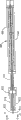
Pin connector 100 (Fig. 4) is preferably configured as and makes it fixing with respect to circuit board 51, and it comprises cover part 108, and this cover part 108 is received in the opening of cover cap of this socket connector 200.This pin connector is formed by a series of parts 101 that are referred to as " thin slice " here, because its structure is thinner.These thin slice 101 sheet stack of laminations of assembling or thin slice pieces 102, they keep together with neat device or retainer 103 as a unit, and this retainer 103 engages a series of grooves 104 that are formed on these connector block 102 back.Cover part 108 also preferably is arranged to be sleeved on the front or the mating surface 109 of connector block 102, and can have formation a series of openings 110 thereon, and these openings align with the terminal mating part or the contact portion (not shown) of this pin connector 100.The terminal 112 of pin connector 100 can terminate in afterbody, the flexible latch 113 of the through hole shown in for example, and this afterbody is received in the corresponding installing hole of circuit board 51.Other erecting device also is in considering, for example mounted on surface, ball grid array etc.
The thin slice of this connector preferably fits together with ternary form so that form single-ended signal transmission and with the order of S-G-S (signal-ground connection-signal), this means that ground connection thin slice or earthing member are arranged between per two signal thin slices.When this thin slice was assembled into their three sheet form (shown in Fig. 6,9,10 and 21), they can be used as three thin slices or single-end sub-component and are disassembled and change, and this will make things convenient for the maintenance and repair of connector of the present invention.
With reference now to Fig. 7 and Fig. 8,, Fig. 7 and Fig. 8 illustrate two thin slices 210 and 220 of socket connector 200.In Fig. 7, signal terminal thin slice 210 is shown, signal and the earth terminal thin slice that aligns mutually with annexation shown in Figure 8.Be to be understood that, the side of the ground connection thin slice 200 that another signal terminal thin slice 210 is exposed from the view of Fig. 8 be can't see, and the terminal assemblies about this embodiment of the present invention comprises two signal terminal thin slices in the relative both sides of centre-point earth terminal thin slice, as shown in Figure 9.
This signal terminal thin slice 210 is supported on here the terminal group 211 that is called " signal terminal set ", and wherein, it comprises the terminal of extension with transmission of electric signals and ground connection reference signal, but does not comprise that extension is with whole structure as ground connection, for example earth shield.Terminal 211 can mold pressing and is formed guide support, and housing parts 215 preferably for example uses inlaying moulded, over-molded (overmolding) or other suitable methods to form with insulating material or dielectric substance around them then.Each terminal has the afterbody 213 that is used to be installed on circuit board 52 and from the contact portion 214 that the edge or the face 218 of this housing (or thin slice) 215 stretches out, is used for matching with the relative contact portion of pin connector 100.Afterbody 213 also stretches out along the another side or the face 600 of this housing 215.These two afterbodys and contact portion are interconnected by terminal bodies part 216 placed in the middle (shown in Fig. 7 dotted line), and it forms the electric pathway by terminal between this contact portion 214 and afterbody 213.
The terminal part in cooperation district of stretching out the front 218 of this connector thin slice/housing 215 can be regarded as and forms sweep 219, and this sweep is arranged between contact portion 214 and this terminal bodies part 216 or this thin slice front 218.As Fig. 2, Fig. 8 and Fig. 9 finding, this sweep 219 comprises central body 222, and its thickness and width are similar to the thickness and the width of terminal bodies part 211.This main part 222 is joined by two Ge Bao Cervical or bend arm 223 sides, and the vertical width (or thickness) of this thin neck or sweep is less than the vertical width of termination contact part, central body or main part (214,222,216).The elasticity that reduces to increase this sweep 219 of size, and thicker main part 222 provides intensity and influence to pass through the electrical characteristics of this terminal of this sweep.It increases the coupling capacitance between this signal and the earth terminal sweep, and this will cause the reducing of this regional impedance of connector.It also increases the electricity of the signal terminal of these relative both sides of ground terminal array and isolates.The size of this sweep main body can be made the desirable impedance magnitude in this part that is implemented in connector.
This sweep is not limited to the structure shown in Fig. 1 to 15, can also take other forms.Figure 39 illustrates two relative terminal assemblies, and wherein, one of this terminal assemblies 900 has another kind of sweep structure.The earth terminal 905 that this terminal assemblies 900 has a plurality of electrically conductive signal terminals 902,904 and supported by insulation shell 901.This earth terminal 905 forms by connecting earthing member, and this earthing member is joined by signal terminal 902,904 sides.This terminal has different sweep 906,907, and it is separated with contact portion by the elongated support bar 910 that extends through these terminals.Thereby the great majority of sweep 906 are straight and linearity.Two sweeps 907 in bottom are shown arcuate shape.This will reduce undesirable size that is formed on the tension force or the pressure of this sweep, the particularly size of the tension force of nethermost sweep or pressure when connector moves.
The terminal supports 225 that is shown elongated vertical rod can be molded in all terminals contact portion 214 on, its purpose will describe in detail below.Just as used herein, term " mating part " or " cooperating the district " refer to the terminal part of stretching out forward from the front 218 of this connector thin slice or housing 210,220.The contact portion of this terminal and sweep are positioned at this and cooperate district or mating part.
Ground connection thin slice 220 (Fig. 8) is configured to similar form and preferably includes earthing member 230, and this earthing member is kept by dielectric or plastic stent 238 or supports.As shown in the figure, in this embodiment, this earthing member has contact portion 232, but does not have afterbody.It depends on its ground connection contact pin 237 that contacts with the earth terminal of appointment, and this earth terminal is in arrays of signal terminals, and this signal terminal has its oneself the afterbody that is used for the connecting circuit plate.
This earthing member 230 comprises flat or main part 231, and this flat or main part 231 have the termination contact part 232 of stretching out forward from it.Be similar to the structure (Fig. 7) of signal terminal set sweep 219, these termination contact parts 232 are connected in this plate main body 231 by sweep placed in the middle 233, and comprise thick central body 234, this central body is joined by two thin bend arm 235 sides, also is provided with vertical support bar 236 so that this earthing member contact portion 232 is held in place in this cooperation district.
For effective ground connection is provided in whole connector system, this ground plate 231 of punching press or mold pressing is to form a plurality of ground connection contact pin 237 of stretching out from this plate 231.These ground strip 237 preferred orientation become to align with the dedicated terminals of this signal terminal set, this dedicated terminals is appointed as and is used to transmit the ground connection reference signal, and they stretch out on the opposite side of this ground plate 231, and as Fig. 9 and Figure 10 clearly shown in, these ground connection contact pin are stretched out from the plane that this ground plate 231 extends.The contact pin of stretching to the left side of the plate among Fig. 8 and Fig. 9 represents with 237a, and the contact pin of stretching to the right side of this plate is represented with 237b.
As shown in Figure 8, this ground terminal set remains in the plastic stent 238 that extends around the periphery of this plate 231.In order to provide and the contacting of the dedicated terminals of this signal terminal set 211, the support 215 of this signal thin slice is bored a hole, and has formation hole 240 thereon.Align with terminal bodies part 216 in these holes 240, so that its part 216a exposes in this hole 240.The ground connection contact pin 237 of this ground plate 231 will extend into these holes 240 and contact the terminal bodies part 216a that this exposes.As shown in the figure, these ground strips are arranged to such figure, so that they pass through to support the insulation shell of this terminal group along with the ground connection reference terminal in the signal terminal set extends.By this way, each trilamellar centre-point earth plate 231 is as being clipped in two middle grounds between the signal thin slice.Because the sort signal terminal structure, this terminal can be arranged to ground connection-signal-ground connection-signal-ground connection and replace vertical order, and wherein the ground connection reference terminal will (vertically) be positioned at the side of signal terminal.The terminal of each terminal assemblies can be easy to be arranged in the horizontal line figure of signal-ground connection-signal in (in the signal terminal of " really " is capable) and the horizontal line figure ground connection-ground connection-ground connection (is in the row of ground connection reference terminal at signal terminal) then.
Figure 10 illustrates three thin slice terminal assemblies 120 of the different structure that is used for pin connector 100.In this three thin slices terminal assemblies 120, utilize two signal terminal set 121 and an earth shield 122.This earth shield 122 is arranged between two signal terminal set 121, and can comprise the corresponding afterbody of contact pin 124 conducts and the contact portion of flexible latch 123 and band slit.This earth shield 122 remains in its oneself 131 dielectric support 130 with central opening, put in termination contact with the appointment of signal terminal set by these central opening 131 its ground connection contact pin 132 by being formed on hole 135 in this dielectric sheet 136, this electrolyte sheet is molded on the guide support of this signal terminal set 121.The contact portion 129 that is shown in the signal terminal set 121 of Figure 10 is female terminal of the pin-type contact portion 214 of receiving socket bonder terminal.Equally, earth shield contact portion 124 is received in the thick slide plate contact portion of earth shield 230 in the slit 177 that is formed between their contact arms.
Turn back to Fig. 2, this socket connector preferably also comprises shade assembly 250, and its part moves as a unit with this termination contact part.This shade assembly 250 comprises clamping element 251, cover cap 252 and key 253.This clamping element 251 has as shown in the figure inverted U-shaped and is fixed on the piece of this connector thin slice.It does not move, and it helps thin slice aligner 103 to keep this connector block as a unit.This clamping element 251 can comprise from its outwardly directed supporting leg 256 and be used to limit this cover cap 252 moving on connector body.
This bending is moved, and as shown in the figure, particularly shown in Figure 11-12 and Figure 14-15, is subjected to this cover cap 252 and the terminal mating part at these support bar 225 places are fixed together as the influence of a unit.This cover cap 252 is not attached to this connector block 201 and moves freely, but support bar 225 covers 252 the unsteady point that forms this terminal that engages with housing, and this terminal shell 210,220 specifically forms fixing points along its front 218.Though housing lid 252 is fixed the support bar 225 with this terminal, this support bar 225 can move with respect to the front 218 of this connector block 201.By this way, and as Figure 12 schematically shown in, the simulation of the sweep of this terminal has 4 mechanical connections of 4 of B1, B2 as shown, B3, B4.This structure allows this contact portion (with this cover cap) to move as one group, simultaneously this contact portion 214,230 is kept their cooperation orientation, and this orientation is preferably and is parallel to each other.
The contact portion that Figure 11 and Figure 12 illustrate this socket (connector) along upward to or+bending (Figure 11) of Y direction and along downward direction or-bending (Figure 12) of Y direction.Figure 13 illustrates the gap between this cover cap 252 and the circuit board 52.Figure 14 and Figure 15 illustrate and occur in the maximum deflection of socket connector along two different directions " X " (left side) and " X " (right side) direction, and this bending occurs in the horizontal plane.
For the cooperation district that this cover cap and this socket connector 200 are provided moves along the uncrossed of these directions, between clamping element 251 and cover cap 252, form gap " C " (Fig. 1 and Fig. 2), make this clamping element not hinder the motion of this cover cap and contacting of it.As shown in figure 13, this cover cap 252 can comprise below this cover cap 252 281 notches 280 that form, and it is used to provide the space between the limit 282 of this cover cap and this circuit board, and this connector is installed in (Fig. 6 and Figure 11-13) on this circuit board.
As shown in the accompanying drawing of Figure 12, this socket connector 200 comprises angled surperficial 290, and it preferably extends around the inner rim of the face 291 of this cover cap 252.This angled surperficial 290 as introduce the surface and in angled surperficial 293 mode of complementation with helping guide this relative pin connector (Fig. 4) to enter in the inside opening of this cover cap 252.
As shown in Figure 7 and Figure 8, this support bar 225 is to cross over or cross the signal of each terminal assemblies or the vertically extending vertical member of bearing of trend of earth terminal contact portion, so that they are vertical and are utilizing in the connector of horizontal array of terminal to be level in the connector of the orthogonal array of utilizing terminal.Like this, they keep the termination contact part of each array of terminals with predetermined contact interval.This support bar by inlaying moulded, over-molded or any suitable assemble method, puts on this terminal as interference fit, bonding etc. in this embodiment best.When this terminal assemblies was assembled together, this support bar adjoined each other then, as shown in Figure 8.The adjacent side of this support bar can have and is used for the device that is bonded with each other with slit 555 forms (Figure 25), bonding etc.
Should be noted that this crooked connector can comprise dielectric rake or pad 275, it separates signal terminal set sweep in each terminal assemblies and ground terminal set sweep.Preferably, with two this pads 275, and be shown and be arranged between signal terminal thin slice 210 and the earth terminal thin slice 220 in each terminal assemblies.As shown in the figure, this pad 275 is elongated and is rectangular substantially that its angled limit 276 is positioned at its pedestal as shown in the figure, so as this pad 275 between the top of this signal and ground terminal array and bottom fully (intersection) extend.This spacers preferably, is connected in this arrays of signal terminals along its inner surface in one of this array of terminals, so that it extends between this signal and earthing member array of terminals.The mode that should be connected by interference engagement in Fig. 7 and embodiment shown in Figure 8 realizes, and this shim elements 275 comprises the lug 277 of U-lag 278 forms that are formed in this gasket body.This connection lug 277 preferably includes the free end 279 of increasing, and it is installed in one of space between the pair of terminal sweep of this arrays of signal terminals.
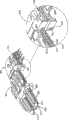
Figure 16 and Figure 17 illustrate an alternative embodiment of the invention, and it includes power supply terminal in this connector.Socket connector 300 is shown in Figure 16, and can see having the parts of many and previously described socket connectors 200 with spline structure, for example retainer 103, comprise clamping element 251 and keep the shade assembly 250 of key 253.It can also comprise a plurality of connector thin slices, three of these connector thin slices are one group and fit together, become three thin slice groups, importantly, it comprises a plurality of power supply terminals (Figure 18), and it forms the part of the whole power terminal set 411 that is supported by insulation shell 423 (Figure 19).
Each power supply terminal 410 comprises mounting portion 415, main part 416, contact portion 417 and is arranged on sweep 418 between this main part 416 and the contact portion 417.This sweep 418 comprises above-mentioned central body 419, and this central body is by two thin bend arm 420 side adjacency.This power supply terminal sweep 419 interconnects by vertical guide 421 during fabrication, and is molded and forms with terminal, as shown in figure 18, but removes from this terminal guide support stamping parts then.Support bar 422 can be overmolded to this power supply terminal as shown in figure 19, and thin slice main body 423 can be molded in all or part power terminal set 411 on.These power supply terminal thin slices can be positioned near signal and earth terminal thin slice, or as shown in figure 16, along a side of this socket connector.In this embodiment, support bar 422 is used for this power supply terminal contact portion 417 is fixed in aforesaid movably cover cap.
Figure 20 and 21 illustrates the terminal group with pin connector 350 uses of Figure 17, and this pin connector uses with the socket connector 300 of Figure 16.This terminal group 351 comprises the signal terminal 352 that extends along power terminal set 353.All these terminals all have mounting portion 360, main part 361 and contact portion 362, they all are preferably the contact portion with band slit, and the contact portion of these band slits will be received in their corresponding slits of contact portion this socket connector 300 or power supply terminal, earth terminal or signal terminal.These terminal group have the dielectric body that is molded on them, and as in the pin connector of Fig. 4, are clipped in wherein around ground terminal set.Wherein one group of signal terminal is shown in Figure 20, and Figure 21 illustrates the pin connector assembly with earth terminal, and this earth terminal is joined by two signal terminal set sides, and each signal terminal set is supported by insulation shell.
Figure 22 illustrates two different plug earth shield structure end embodiment with Figure 23, and it illustrates plug and socket connector of the present invention and how to be combined together.Can see that this structure is a slip joint, wherein the ground connection contact portion of socket connector is installed by hole 110 and is engaged in the pin connector cover 108, and clamps by a pair of contact arm 191, and this clamp arm is embossed in its contact portion.In Figure 22, the ground connection slide plate 230 of socket connector terminal extends into vertical mode in the slit 190 between two contact arms 191 that are formed on the pin connector terminal assemblies.Figure 23 A is shown specifically connector of the present invention " little intersection ".
In Figure 23, the socket connector terminal assemblies is shown horizontal alignment, rather than is shown vertical orientatedly as previous drawings, and pin connector terminal assemblies 136 is shown vertical orientated, and for the sake of clarity, the free end 214 of termination contact part has been removed.The contact slide plate 230 of this earthing member is received in the slit 190 between contact arm is to 191.By this way, the ground connection of two connectors intersect in the cross mode and between arrays of signal terminals vertical extent, but also between rows of terminals horizontal-extending.This schematically is shown in Figure 23 A, and wherein the cross figure of ground connection 900 is formed on and cooperates the district.Cooperate the district at this, concave contactor 129 cooperations of the signal terminal 214 of socket connector and relative pin connector, and the ground connection contact portion 124,230 of each connector with shown in mode cooperate.This structure separates signal terminal by the ground plane that intersects, and simultaneously, the cooperation interface by two connectors provides continuous ground connection reference.
Figure 24 to Figure 38 illustrates another embodiment of the connector 500 of constructed in accordance with the principles.In Figure 24, two opposing connector assemblies 501,502 only are shown for the sake of clarity.A plurality of connectors 501,502 fit together and are contained in the aforesaid cover cap.This assembly has terminal structure, and this terminal structure can link together two circuit boards 503,504 (being shown in broken lines) them with orthogonal manner.This assembly 501,502 is configured such that at least in them, assembly 501, and structure similar and recited above has can be on X and Y both direction crooked terminal structure.Be similar to other embodiment recited above, the terminal of assembly 501 has the sweep 505 that is arranged between its contact portion and the body/tail, makes that the contact portion of earth terminal and signal terminal can be along the distance of the crooked preliminary election of desirable direction.Therefore, assembly 501 can be referred to as " flexible " assembly, and assembly 502 comparatively speaking can not be as assembly 501 bending motion, and assembly 502 can be referred to as " fixing " connector assembly.
Each connector assembly can be regarded at least three as, the combination of the subassembly of common four conductions.For flexible connector assembly 501, the subassembly of these conductions can comprise first group or second group or second array 513 of first array 512 and signal terminal of first group of (as Figure 28 and shown in Figure 31) earth terminal or first array 510, earth terminal second group or second array 511, signal terminal.As Figure 28,31 and 32 clearly shown in, first and second groups of earth terminal are set together in mode side by side, so that they preferably adjoin each other with independent, the shared grounding that forms double-thickness with reference to 520 (Figure 30,31 and 32).These two ground connection can be regarded center reference or the line that cooperation ground constitutes or form flexible connector assembly as.Consider that also single earthing member can be used for this application.
These first and second groups of signal terminals 512,513 are arranged on the relative both sides of this shared grounding 520.Preferably, wish that first and second groups of signal terminals 512,513 also are arranged to so that at terminal and second group of 513 corresponding terminal horizontal alignment of first group 512, as Figure 31 and shown in Figure 32.Also wish the signal terminal of first and second groups of signal terminals 512 and 513 spaced apart, so that a pair of " P " of the terminal of this first group of terminal 512 is (Figure 32) in a side of shared grounding 520, and a pair of " P2 " of the terminal of second group of terminal 513 is at the opposite side of shared grounding 520, by this way, form decussate texture or figure, and shared grounding 520 extends (Figure 31) downwards along the center of figure with " CF " expression.In addition, the location of signal terminal 512,513 makes its top and bottom margin (along the line " D " of Figure 31 and 32) align with the vertical end 580 of shared ground connection 520, so that keep the electric affine of they and this ground connection 520, rather than it is mutual electric affine, if the end of signal terminal 512,513 extends on the D line, it takes place equally.The end that Figure 31 illustrates signal terminal 512,513 keeps the end 580 same height with ground connection 520, and Figure 32 illustrates this end and is positioned to be lower than the D line.
This cross figure is realized by the structure and the layout of signal terminal contact portion 530, this signal terminal contact portion is extended forward from the sweep 531 of this terminal, and aforesaid terminal support bar preferably forms and is installed in cover cap or other supports with insulating material.The termination contact part 530 of this terminal assemblies forms shape substantially, and two shank 533 junction between it combines.As shown in the figure, two of each signal terminal contact portion 512 shanks 533 leave (in parallel substantially and vertical) along shared grounding 520 extensions and from it.Because two shanks 533 combine, they are characterized by " integral body " contact portion in this specification.This contact portion 530 and sweep 53 partly are connected in afterbody 535 by the terminal bodies that is supported by insulation shell 540.The shape of this terminal provides the intensity and the redundancy of signal contact portion.
Figure 33 at length illustrates the sandwich of this flexible connector assembly 501 or stratification structure.First and second windings ground terminal 510,511 has contact portion, it preferably takes the form of flat contact slide plate, it adjoins each other to form shared grounding 520, but, as shown in figure 30, they scatter mutually in the zone of the sweep 531 that is arranged in terminal support bar 532 rear portions (Figure 30).First and second signal terminal set 512,513 are partly laid or are enclosed in the insulating body 540,541 (Figure 29 and 30), the main part that it supports and surrounds this terminal at least in part.This tail portion of terminal 535 is stretched out from a side of these insulating bodies 540,541, and contact portion is stretched out from opposite side, preferably stretches out from a side that is adjacent.
Be in operation, the insulating body 540,541 that these first and second groups of signal terminals 512,513 are installed is assembled on this first and second windings ground terminal and in its relative both sides, to form this laminar fixed connector subassembly 501.If wish between it, to provide dielectric substance, so Fu Jia insulation spacer element 544 (Figure 33) can be arranged between sweep zone 531 interior first and second terminals 512,513 and the earth terminal 510,511, to prevent unexpected short circuit between this regional signal terminal and earth terminal, should additional insulation spacer element 544 can be resolution element, or form a part or its extension of this insulating body 540,541.Embodiment as the front is described, and this whole terminal assemblies can be used as individual unit and inserts pin connector or socket connector and pull down from it, thereby does not need to safeguard and/or repair the whole assembly of this connector.
As Figure 27 and Figure 38 clearly shown in, this fixed connector subassembly also comprises corresponding relative terminal.These terminals comprise first and second windings ground terminal 550,551, and it has flat slide plate contact portion 552.This first and second earth terminal adjoins each other in contact portion zone 552.These terminal combination are formed on the center shared grounding 52 that extends between first and second signal terminal set 560,561, and preferably extend downwards along the center of this connector assembly 502.This first and second terminal group 560,561 is also partly centered on by insulating body 567,568, and it is used to prevent unexpected short circuit between this signal terminal and the earth terminal.Should be appreciated that if desired as described with respect to other embodiment of the present invention, signal can bend to relative ground connection with the earth terminal part and contact with signal terminal.
Turn back to Figure 38, can see, the contact portion of this first and second terminal 560,561 also is a shape roughly.These contact portions are different from flexible connector assembly " integral body " contact portion 530, are that they comprise bifurcated or the two contact arms that separated by interval placed in the middle 574, or beam 572,573.These contact arms 572,573 extend forward from main part 575, and contact arm 572,573 be arranged in case they one of partly extend along the earth terminal slide plate, and this earth terminal slide plate part (roughly in parallel and vertical) is left in their another extension.These contact portions 570 also are provided with in pairs, join (Figure 34) with every side side of shared ground connection, and this first group of signal terminal preferably align with the contact portion of second group of signal terminal, as representing with P and P2 among Figure 35.They also preferably are arranged to the cross figure, so that they cooperate with the L shaped contact portion of flexible connector assembly easily.This pair contact arm has different length, and a longer contact arm so that when cooperating, is somebody's turn to do short contact arm deflection easily in the scope of another contact arm in another.
This is shown in Figure 37 and Figure 38, wherein, can see contact length that this horizontally extending contact arm part 572 (when terminal assemblies keep to be erect) the has length greater than vertically extending contact arm 573.In this respect, the free end 902 of this contact arm 573 can be along the path free deflection of arrow among Figure 37, and in this scope, or move in " cap " of another contact arm, and do not disturb the free end 903 of this another contact arm 572.The difference of this length also influences the scope of each contact arm deflection, and reduces the maximum insertion force of connector.This minimizing obtains with integral contact 530 contacts of their relative socket connector by this paired contact arm half (every centering is than one of length), and should contact this relative integral contact 530 than the contact arm of weak point subsequently.
Figure 24 A is an enlarged detailed, and the engage of the contact terminal assembly of these two shapes is shown.As shown here, this horizontal contact arm part 572 is first and the surface that contacts beam 512 533 slip joint of this integral body shape in two contact arm parts 572,573.This initial maximum insertion force includes only this long contact arm 572 and cooperates needed power with the whole beam 512 that contacts, rather than two contact arms 572,573 cooperate needed power simultaneously.
This embodiment comprises that also use is in " little intersection " structure shown in the sectional view of Figure 24 B-24D.Figure 24 B is the sectional view along its B-B line intercepting, four groups of terminals with stationary terminal.In this sectional view, contact arm 572,573 is arranged to L shaped orientation and spaced apart with this dual ground connection 521 as shown in the figure.Shown in Figure 24 C that the C-C line along Figure 24 A intercepts, in the cooperation district, these two shared groundings, 520,521 insertions fixing and flexible terminal assemblies intersect with the signal terminal of formation with two connector assemblies, as shown in the figure.Along among Figure 24 D of the D-D line of Figure 24 A intercepting, the interval that this sweep is arranged to equate, and align with the opposite side of the shared grounding 521 of this stationary terminal.By this way, this signal terminal and ground connection remain on desirable interval to help the coupling between this signal terminal and this ground connection.
Shown in the use of dual ground connection be useful, because main part at this connector assembly, this ground connection is spaced from each other, so that each this earth terminal provides reference for the signal terminal near it, and be adjacent and and its signal terminal that leaves between provide electricity to isolate, that is, in Figure 30,510 pairs of signal terminals 512 of earth terminal of this main part subregion provide ground connection with reference to and with the isolation of signal terminal 513.Shown in Figure 31-32, this signal terminal 512,513 can with reference ground connection 520 G1 spaced apart (Figure 32), this apart from G1 less than between the corresponding signal terminal 512A of it and adjacent signals terminal assemblies apart from G2, as shown in figure 31.
Another embodiment of the connector assembly of constructed in accordance with the principles is shown in Figure 40-55.In embodiment described below, for each terminal assemblies provides ground structure, its point that enters its supporter from this terminal leaves the point of this supporter to them, follows or total length of " tracking " each signal terminal by this terminal assemblies.By this way, this ground structure partly surrounds each signal terminal.
As shown in figure 40, connector assembly 990 is used for two circuit boards 1001,1201 are linked together.Shown connection shows that making quadrature connects, but the orientation that should be appreciated that each connector also can be used for such as parallel orientation etc.This connector assembly 990 utilizes the connector component of two cooperations, and one of them shows and makes hollow socket connector, or head connector 1200 (Figure 41-46), and another shows and makes outstanding convex or pin connector 1000 (Figure 47-55).
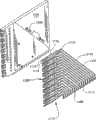
Shown in Figure 41 and 43, this head connector 1200 can comprise hollow holder,head 1202, and it has a plurality of spaced crossing walls, so that form a plurality of hollow sockets 1204.Each socket is laid conducting terminal structure 1206, and it comprises signal and earth terminal.Two support bars 1203 can be used for this head piece is kept together as single unit.In this respect, this holder,head 1202 can be formed by a plurality of single socket support or unit 1202 as shown in figure 43, and perhaps it can comprise and forms single socket support with a plurality of receptacle openings.
Such terminal structure 1206 is shown in Figure 44 and it comprises the different conducting terminal groups or the structure of array 1207-1209.This terminal is arranged in such a way, make winding ground terminal group, or earth terminal central line array 1208 is preferred with the formation of single-piece electric conducting material, usually formed by the sheet material with base part 1220 and a plurality of contact portion 1221, this contact portion illustrates with the form of the flat contact slide plate that stretches out from this base part 1220.Afterbody 1212 also forms the part of this terminal group 1208, and shows in Figure 45 and do or mounted on surface afterbody 1409, perhaps a plurality of soldered balls 1222, and it is set to the ball grid array part.Also can for example compress contact, submissive latch etc. with other afterbody.
The center array of earth terminal 1208 is joined by the linear array side of signal terminal 1209 in both sides, and these array of terminals 1209 also comprise pedestal 1210, though they are formed by the base part of the conduction of insulating material rather than this ground terminal array.The contact portion 1225 of this signal terminal 1209 forms above-mentioned form and contacts slide plate as the integral body of Figure 31 and the shape shown in 32, but this terminal does not form any sweep.This contact portion 1225 is stretched out on this arrays of signal terminals base part 1210 and is left from it, and this signal terminal 1209 also has afterbody, and this afterbody does not illustrate in Figure 45, but it by or stretch out from the base part 1210 of its insulation.
At last, each terminal assemblies of this socket connector preferably includes pair of end portions earth terminal component, or array of terminals 1207, its each have the conductive base part 1226 of straight line, from its afterbody that stretches out 1221 and contact portion 1227.By this way, the signal terminal of each jack connector assembly will be grounded terminal and be centered on form of straight lines, to form the structure (or G-S-G-S-G shown in Figure 45) of earth terminal-signal terminal-earth terminal-signal terminal-earth terminal.This terminal assemblies 1206 will match with the terminal assemblies 1100 of the pin connector 1000 of relative cooperation.By this way, as shown in the figure, this signal terminal set 1209 is joined by ground terminal set 1207 or 1208 sides in both sides at the Width of socket connector 1200.This ground terminal array the 1207, the 1208th is different.As shown in figure 45, this centre-point earth array of terminals 1207,1208 has thin contact portion 1227.Preferably, these ground terminal array contact portions 1221,1227 are alignd mutually at Width, or the linear array of the terminal of this jack connector assembly 1206 of lateral cross.
Figure 46 illustrates the pin connector 1000 that is used for the connector assembly of the present invention that matches with head connector 1200.As shown in the figure, this pin connector 1000 comprises housing 1002, and its encirclement is installed on a plurality of terminal assemblies (not shown) of circuit board 1001.Cover part 1003 constitute these connector parts and be used for covering its terminal assemblies contact portion stretch out cooperative end part.This housing 1002 forms hollow casing, usually has unlimited front and back side, it is admitted each terminal assemblies within it, and they are held in the orientation of preliminary election, wherein each terminal assemblies remains in the single passage 1300, and this single passage is formed in this shell by a series of guide rails 1302 that are formed on this shell inner surface 1303.These guide rails, as Figure 46 and 46A clearly shown in, have "T"-shaped shape and they are along the slit 1305 splice terminal assemblies that form thereon.
One of a plurality of terminal assemblies 1100 of this pin connector 1000 show at Figure 47 makes exploded view.As shown in the figure, plug terminal assembly 1100 comprises centre-point earth terminal supports 1103, and it has a plurality of contact portion 1103A that show the contact of making dual band slit.This centre-point earth terminal supports is joined by two signal terminal strutting pieces, 1101,1102 sides of shell form, and each comprises insulation shell 1130 this signal terminal strutting piece, and it can be molded on the conducting terminal group 1104,1105.This signal terminal shell 1101,1102 is joined by a pair of earthing member 1106,1108 sides equally, this earthing member is preferably taked the form of flat surface plate, it has the contact portion 1107,1106 of stretching out from it on one side along it, and the afterbody 1125 that stretches out from it along its another side.This earthing member that this contact portion and afterbody stretch out from it is that mutual vicinity preferably is arranged on two limits as shown in the figure.
Figure 47 A illustrates all parts that fit together this terminal assemblies that is assembled into an assembly.In this assembly, two signal terminal strutting pieces 1101,1102 and centre-point earth spare 1103 are bonded with each other together, and the earthing member 1106,1108 on two planes is applied in the end of this assembly 1100.The main part on the plane of this end earthing member 1106,1108 preferably is received within the corresponding grooves 1131 of the outside that is formed at this signal terminal strutting piece 1101,1102.
Figure 49 illustrates the signal terminal strutting piece 1102 on the right side, and it is illustrated as the guide support 1105 that separates with signal terminal housing or shell 1131.The guide support of this conduction comprises contact portion 1112, afterbody 1111 and the main part 1110 that this contact portion and afterbody are linked together.As shown in figure 50, these a plurality of terminals are connected bar 1113 and link together, its in this terminal assemblies is installed in its insulation shell before by the cutting or the cutting be removed.This terminal group preferably is installed on housing 1130 by the terminal supports shell is inserted or is molded on this terminal group 1105.The contact portion 1112 of the signal terminal set 1105 of this pin connector preferably includes paired contact arm 1117,1118, and this contact arm stretches out from the Different Plane of main part 1116.The length that is shorter in length than another contact arm 1117 of contact arm 1118 is so that these two contact arm mutually noninterferes mutually when this terminal group cooperates with the signal terminal of head connector.As mentioned above, contact arm 1117,1118 is arranged to shape, so that two contact arms contact with the contact arm of the socket connector of two relative cooperations.
Figure 48 illustrates two relative centre-point earth terminal supports 1103 isolated signal terminal strutting pieces 1101,1102.This signal terminal housing 1130 can have bar 133 and in order to assemble the opening 1134 that cooperatively interacts together, and can be with holding them in together such as ultra-sonic welded, plasticity welding, interference engagement, various methods of attachment such as bonding.
In an importance of the present invention, and shown in Figure 51, centre-point earth terminal supports 1103 comprises the centre-point earth plate 1120 of conduction, and this centre-point earth plate has afterbody 1122 and the contact portion 1103A, 1123 that is formed on its different edges.This contact portion 1103A is the beam contact of band slit, and is orientated to 1,221 90 ° of the contact slide plates of the ground terminal set that departs from this socket connector 1204, and other contact portions 1223 are set in case of necessity.By this way, be similar to reference to the connector end sub-component shown in Figure 31 and 32 described, contact zone at two connectors 1000,1200 forms intersection or cross figure, promptly, the contact portion 1123 of the centre-point earth spare 1103 of each pin connector terminal assemblies 1100, at a certain angle or perpendicular to the array of this terminal, engage this socket connector centre-point earth array of terminals contact portion part.The final result of this cooperation, by its cooperate the district and basically along the connector of these two cooperations from the circuit board to the circuit board, array or " box " of shielding is provided around each signal terminal of connector assembly basically.
This centre-point earth plate 1120 has the main part 1121 (Figure 48 A) on plane, and this main part has one or more along the maintenance bar 1124 that forms thereon on one side.This plate 1120 comprises along homonymy not from its afterbody that stretches out 1122 and contact part 1103A, 1123.This ground plate 1120 is enclosed in dielectric housing or the shell 1125, this housing or shell are preferably used mouldable material, for example plastics form, and have the passage that a plurality of upborne platforms 1127 sides join or cave in 1126, on the opposite side of this housing 1125, to form level and smooth a little joint effectively.This earthing member can be molded on this housing 1103, or is stuck in (not shown) between the two halves that two mutual connection closes in another way.The outer surface of this housing 1125 preferably conducts electricity, and can by the plating molding technology to this material electroplate make its conduction.By this way, as Figure 51 and 52 clearly shown in, actual metal earthing member surrounds with dielectric substance, this material is also electroplated at its all substantially outer surface, so that whole earthing member 1103 is formed shielding, or ground connection.The coating of the conduction on the outer surface of this centre-point earth terminal supports contacts this centre-point earth plate 1120, so that this centre-point earth terminal supports is as single integral ground spare.
Signal terminal strutting piece 1101,1102 (Figure 48) also have platform 1161 and depression 1162 figures towards interior outside 1160, it forms with alternate form, and is arranged to relative with depression with the platform of ground connection strutting piece 1120.The signal terminal strutting piece will be received within the complementary passage and platform of relative centre-point earth terminal supports like this.Pillar 1165 can be arranged on the signal terminal supporting housing 1130, it is equipped with the through hole 1166 in the maintenance contact pin 1124 of this center shield part 1140, so that signal end component 1101,1102 is kept together, and help this centre-point earth terminal supports 1103 is clamped between it.These posts can be used for these whole terminal assemblies 1100 ultra-sonic welded are in the same place with the hole.By this way, the plate surface of centre-point earth spare is used for providing the ground connection reference along three sides (except centre-point earth spare) of each signal terminal.This form with sectional view is shown in Figure 54.The plating part of centre-point earth spare forms three sides that separate of " shielding box " effectively, it can be regarded as by external ground plate 1106,1108 and seals, one of them plate 1108 is maintained in the groove 1131, and another of two plates 1106 separates slightly with the edge of this thin slice 1102, perhaps two plates all be maintained at form with the signal terminal supporting housing on groove 1131 in.
Shown in Figure 47 A, between the signal terminal strutting piece 1101,1102 that centre-point earth terminal supports 1103 is entirely remained on or " card " joins in two side.By this way, in by its scope of pin connector 1101, provide reliable shielding for signal terminal.This shielding can be used in the application of high speed single-ended signal transmission connector of the present invention, is not differential signal application.Cavity 1425 can be formed near (Figure 55) in the terminal assemblies of soldered ball afterbody 1222.
This spatial relationship help to have its around the signal terminal of each terminal assemblies of relevant centre-point earth between capacitive coupling, capacitive coupling between the signal terminal of the signal terminal of a unfavorable and terminal assemblies and adjacent terminal assemblies, and thisly will cause cross interference and noise when being coupling in the high-frequency data transmission.
Claims (13)
1. one kind is used for high density, high speed connector (1000) that two circuit boards (1001,1201) are interconnected, and this connector (1000) comprising:
Connector shell (1002), be supported on the group of a plurality of different terminal assemblies (1104,1105) in this connector shell (1002), each terminal assemblies (1104,1105) comprises a plurality of afterbodys (1111) that are used for this terminal is connected in circuit board (1101), with be used for and the contacted a plurality of contact portions of the terminal of the connector that matches (1200) (1112), each different terminal group comprises centre-point earth terminal supports (1102) and at least two signal terminal strutting pieces (1101,1102), it is characterized in that:
This centre-point earth terminal supports (1103) comprises the centre-point earth plate (1120) of the conduction of a plurality of contact portions (1103A, 1103B) that have from its extension, and this centre-point earth plate (1120) is sealed in outside dielectric shell (1125), and this centre-point earth terminal supports outer enclosure (1125) has the conductive coating that setting contacts with centre-point earth plate (1120) on its outer surface; And
Described at least two signal terminal strutting pieces (1101,1102) array of signal terminal of the conduction of two arrays is arranged in each support, each signal terminal of this array comprises the contact portion (1112) of the afterbody (1111) that is used for connecting circuit plate (1101) and the connector that is used to be connected cooperation, and with connect together main part (1110) of this signal terminal afterbody (1111) and contact portion (1112), each signal array is maintained at the dielectric enclosure (1130 of outside separately, 1131) in, this signal terminal shell (1130,1131) be arranged on the opposite side of described centre-point earth terminal supports (1103), each signal terminal shell (1130,1131) comprise the platform (1161) of a plurality of risings, its passage (1162) that occupy therebetween that is formed thereon separates, and the described main part (1110) of described arrays of signal terminals is sealed in the platform (1161) of described signal terminal strutting piece rising; And
Each described terminal assemblies also comprises pair of outer ground plate (1106,1108), it is arranged on the outer surface of this signal terminal shell, and spaced apart with this centre-point earth terminal supports and signal terminal, each described external ground plate (1106,1108) comprises the contact portion from its extension.
2. connector according to claim 1, the surface of wherein said centre-point earth terminal supports conduction and this external ground plate (1106,1108) form the passage of four sides shielding, and this groove extends the length of described arrays of signal terminals terminal bodies part.
3. connector according to claim 1, wherein said centre-point earth terminal supports (1103) also comprise a plurality of passages (1126) and are arranged on the platform (1127) of the rising on its opposite side.
4. connector according to claim 3, wherein the platform (1127) of each described centre-point earth terminal supports passage (1126) and rising extends in the path between two adjacent edges of described centre-point earth terminal supports (1103).
5. connector according to claim 3, the platform (1161) that wherein said signal terminal strutting piece raises is received in the described centre-point earth terminal supports passage (1126), and the platform (1127) that the passage of described signal terminal strutting piece (1162) admits described centre-point earth terminal supports to raise.
6. connector according to claim 1, wherein said arrays of signal terminals terminal tails comprises soldered ball (1222), and wherein said signal terminal supporting housing (1101,1102) comprises a plurality of cavitys (1425) that form along its edge, and each cavity (1425) is arranged near single soldered ball (1222).
7. connector according to claim 1, wherein said connector shell (1102) is included in inside formation a plurality of guide rails (1302) thereon of described connector shell (1102), this guide rail (1302) forms a plurality of single slits (1300), and each slit (1300) is received in signal terminal assemblies wherein.
8. connector according to claim 7, wherein said terminal assemblies comprise the slit (1305) that is provided with along its limit, and this slit (1305) is admitted the guide rail (1302) of described connector shell.
9. connector according to claim 1, wherein said centre-point earth terminal supports (1103) is stuck between described two signal terminal strutting pieces, makes to have only described centre-point earth terminal board afterbody (1122) and contact portion (1103A, 1123) to stretch out from described terminal assemblies.
10. connector according to claim 1, wherein said signal terminal contact portion (1112) comprise the L shaped contact portion (1117,1118) of many offsides facing to centre-point earth termination contact part (1103A, 1123).
11. connector according to claim 1, each of the terminal assemblies of wherein said connector have the contact portion (1103A, 1123) of described centre-point earth terminal supports (1103), signal terminal strutting piece (1101,1102) and the ground plate of being arranged to ground connection-signal-ground connection-signal-ground connection order.
12. one kind is used for high density, high speed connector assembly that two circuit boards (1001,1201) are interconnected, this connector assembly comprises:
Pin connector that connects (1000) and socket connector (1200);
This pin connector comprises the connector shell (1002) of insulation, be supported on the terminal assemblies of a plurality of different group in this connector shell (1002), each terminal assemblies comprises a plurality of afterbodys that are used for this terminal is connected in circuit board, with the contact portion of the terminal of a plurality of connectors that are used for contact matching, each different terminal group comprises centre-point earth terminal supports (1103) and at least two signal terminal strutting pieces (1101,1102);
This centre-point earth terminal supports (1103) comprises the centre-point earth plate (1120) with a plurality of conductions from its contact portion of stretching out (1103A, 1123), this centre-point earth plate (1120) is sealed in the outside dielectric enclosure (1125), and this centre-point earth terminal supports outer enclosure (1125) has the conductive coating that setting contacts with this centre-point earth plate (1120) on its outer surface;
Described at least two signal terminal strutting pieces (1101,1102) array of signal terminal of the conduction of two arrays is arranged in each support, each signal terminal of this array comprises afterbody (1111) that is used for connecting circuit plate (1001) and the contact portion that is used to be connected the connector that matches (1112), and with connect together main part (1110) of this signal terminal afterbody (1111) and contact portion (1112), each signal array is maintained at outside dielectric enclosure (1130 separately, 1131) in, this signal terminal shell (1130,1131) be arranged on the opposite side of described centre-point earth terminal supports (1103), each signal terminal shell (1130,1131) comprise the platform (1161) of a plurality of risings, its passage (1162) that occupy therebetween that is formed thereon separates, and the described main part (1110) of described arrays of signal terminals is sealed in the platform (1161) of described signal terminal strutting piece rising;
Each described terminal assemblies also comprises pair of outer ground plate (1106,1108), it is arranged on this signal terminal shell (1130,1131) on the outer surface, and it is spaced apart with this centre-point earth terminal supports (1103) and signal terminal, each described external ground plate (1106,1108) comprise contact portion (1106A from its extension, 1107), described centre-point earth terminal supports (1103), signal terminal strutting piece (1101,1102) and ground plate contact portion (1106A, 1107) be set in the described pin connector housing (1102), to form the alternate succession of earth terminal-signal terminal-earth terminal-signal terminal-earth terminal;
This socket connector (1200) comprises the hollow insulation shell (1202) of the outside that forms inner socket (1204), this socket (1204) comprises the signal terminal and the earth terminal of a plurality of conductions that set within it, this signal terminal is insulated supporting base (1210) and is supported in the described socket (1204), and each described signal terminal comprises afterbody (1409) and in the contact portion (1225) of its opposite end, described signal terminal is spaced from each other along insulation supporting base (1210), to form the linear array of signal terminal, described socket (1204) comprises at least two linear arraies of described signal terminal, this earth terminal is with at least the first and second different linear arraies (1207,1208) form is arranged in the described socket, this first ground terminal array (1207) comprises base part (1226) and a plurality of contact portion (1227) and afterbody (1409) that stretches out from the opposite side of this base part (1204) of conduction, and second ground terminal array (1208) also comprises base part (1220) and a plurality of contact portion (1221) and afterbody (1409) that stretches out from the opposite side of this base part (1220) of conduction, described signal terminal (1209) and described earth terminal first and second array of terminals (1207,1208) with the alternate succession setting of earth terminal-signal terminal-earth terminal-signal terminal.
13. connector assembly according to claim 12, the linear array of terminals of wherein said socket connector is arranged perpendicular to described pin connector terminal assemblies.
Applications Claiming Priority (2)
| Application Number | Priority Date | Filing Date | Title |
|---|---|---|---|
| US43077502P | 2002-12-04 | 2002-12-04 | |
| US60/430,775 | 2002-12-04 |
Publications (2)
| Publication Number | Publication Date |
|---|---|
| CN1739223A CN1739223A (en) | 2006-02-22 |
| CN100524954C true CN100524954C (en) | 2009-08-05 |
Family
ID=32469528
Family Applications (1)
| Application Number | Title | Priority Date | Filing Date |
|---|---|---|---|
| CNB2003801090128A Expired - Fee Related CN100524954C (en) | 2002-12-04 | 2003-12-04 | High-density connector assembly with tracking ground structure |
Country Status (3)
| Country | Link |
|---|---|
| US (1) | US20040224559A1 (en) |
| CN (1) | CN100524954C (en) |
| WO (1) | WO2004051809A2 (en) |
Families Citing this family (107)
| Publication number | Priority date | Publication date | Assignee | Title |
|---|---|---|---|---|
| TWM249237U (en) * | 2003-07-11 | 2004-11-01 | Hon Hai Prec Ind Co Ltd | Electrical connector |
| US7094102B2 (en) | 2004-07-01 | 2006-08-22 | Amphenol Corporation | Differential electrical connector assembly |
| US7108556B2 (en) * | 2004-07-01 | 2006-09-19 | Amphenol Corporation | Midplane especially applicable to an orthogonal architecture electronic system |
| US8444436B1 (en) | 2004-07-01 | 2013-05-21 | Amphenol Corporation | Midplane especially applicable to an orthogonal architecture electronic system |
| WO2006091595A1 (en) * | 2005-02-22 | 2006-08-31 | Molex Incorporated | Differential signal connector with wafer-style construction |
| KR20070119717A (en) * | 2005-03-31 | 2007-12-20 | 몰렉스 인코포레이티드 | High-density, robust connector with dielectric insert |
| US6986682B1 (en) * | 2005-05-11 | 2006-01-17 | Myoungsoo Jeon | High speed connector assembly with laterally displaceable head portion |
| US20090291593A1 (en) | 2005-06-30 | 2009-11-26 | Prescott Atkinson | High frequency broadside-coupled electrical connector |
| US7914304B2 (en) | 2005-06-30 | 2011-03-29 | Amphenol Corporation | Electrical connector with conductors having diverging portions |
| US7431616B2 (en) * | 2006-03-03 | 2008-10-07 | Fci Americas Technology, Inc. | Orthogonal electrical connectors |
| US20070207632A1 (en) * | 2006-03-03 | 2007-09-06 | Fci Americas Technology, Inc. | Midplane with offset connectors |
| US7331830B2 (en) * | 2006-03-03 | 2008-02-19 | Fci Americas Technology, Inc. | High-density orthogonal connector |
| US7407413B2 (en) | 2006-03-03 | 2008-08-05 | Fci Americas Technology, Inc. | Broadside-to-edge-coupling connector system |
| US7318757B1 (en) | 2006-06-30 | 2008-01-15 | Fci Americas Technology, Inc. | Leadframe assembly staggering for electrical connectors |
| US7309257B1 (en) * | 2006-06-30 | 2007-12-18 | Fci Americas Technology, Inc. | Hinged leadframe assembly for an electrical connector |
| US7500871B2 (en) | 2006-08-21 | 2009-03-10 | Fci Americas Technology, Inc. | Electrical connector system with jogged contact tails |
| US7497736B2 (en) | 2006-12-19 | 2009-03-03 | Fci Americas Technology, Inc. | Shieldless, high-speed, low-cross-talk electrical connector |
| US7422444B1 (en) * | 2007-02-28 | 2008-09-09 | Fci Americas Technology, Inc. | Orthogonal header |
| US7811100B2 (en) | 2007-07-13 | 2010-10-12 | Fci Americas Technology, Inc. | Electrical connector system having a continuous ground at the mating interface thereof |
| JP4978788B2 (en) * | 2007-08-10 | 2012-07-18 | 住友電装株式会社 | Joint connector |
| DE202007012719U1 (en) * | 2007-09-11 | 2007-11-22 | Rosenberger Hochfrequenztechnik Gmbh & Co. Kg | Multiple micro-HF-contact arrangement |
| US20090130918A1 (en) * | 2007-11-20 | 2009-05-21 | Tyco Electronics Corporation | High Speed Backplane Connector |
| US8469720B2 (en) * | 2008-01-17 | 2013-06-25 | Amphenol Corporation | Electrical connector assembly |
| US8764464B2 (en) | 2008-02-29 | 2014-07-01 | Fci Americas Technology Llc | Cross talk reduction for high speed electrical connectors |
| TWM383226U (en) * | 2008-09-09 | 2010-06-21 | Molex Inc | Connector with improved manufacturability |
| EP2332217B1 (en) * | 2008-09-30 | 2012-08-01 | Fci | Lead frame assembly for an electrical connector |
| DE102009015462B4 (en) * | 2008-11-10 | 2014-10-30 | Erni Production Gmbh & Co. Kg | Angle connector with a shield and method of making the shield of the angle connector |
| MY164930A (en) | 2008-11-14 | 2018-02-15 | Molex Inc | Connector with terminals forming differential pairs |
| US8167651B2 (en) * | 2008-12-05 | 2012-05-01 | Tyco Electronics Corporation | Electrical connector system |
| US7819697B2 (en) * | 2008-12-05 | 2010-10-26 | Tyco Electronics Corporation | Electrical connector system |
| US7871296B2 (en) * | 2008-12-05 | 2011-01-18 | Tyco Electronics Corporation | High-speed backplane electrical connector system |
| CN102318143B (en) * | 2008-12-12 | 2015-03-11 | 莫列斯公司 | Resonance modifying connector |
| US7988456B2 (en) * | 2009-01-14 | 2011-08-02 | Tyco Electronics Corporation | Orthogonal connector system |
| US9277649B2 (en) | 2009-02-26 | 2016-03-01 | Fci Americas Technology Llc | Cross talk reduction for high-speed electrical connectors |
| US8366485B2 (en) | 2009-03-19 | 2013-02-05 | Fci Americas Technology Llc | Electrical connector having ribbed ground plate |
| US8550861B2 (en) | 2009-09-09 | 2013-10-08 | Amphenol TCS | Compressive contact for high speed electrical connector |
| US8267721B2 (en) * | 2009-10-28 | 2012-09-18 | Fci Americas Technology Llc | Electrical connector having ground plates and ground coupling bar |
| US8616919B2 (en) | 2009-11-13 | 2013-12-31 | Fci Americas Technology Llc | Attachment system for electrical connector |
| US7988491B2 (en) * | 2009-12-11 | 2011-08-02 | Tyco Electronics Corporation | Electrical connector having contact modules |
| TWI519011B (en) * | 2009-12-29 | 2016-01-21 | 太谷電子公司 | Electrical connector system |
| CN107069274B (en) | 2010-05-07 | 2020-08-18 | 安费诺有限公司 | High performance cable connector |
| CN101872908B (en) * | 2010-06-09 | 2012-07-25 | 四川华丰企业集团有限公司 | High-speed signal connector |
| US8408939B2 (en) * | 2010-11-19 | 2013-04-02 | Tyco Electronics Corporations | Electrical connector system |
| JP5727765B2 (en) * | 2010-11-30 | 2015-06-03 | 富士通コンポーネント株式会社 | connector |
| JP5595289B2 (en) * | 2011-01-06 | 2014-09-24 | 富士通コンポーネント株式会社 | connector |
| US8636543B2 (en) | 2011-02-02 | 2014-01-28 | Amphenol Corporation | Mezzanine connector |
| CN102694308B (en) * | 2011-03-22 | 2014-09-24 | 富士康(昆山)电脑接插件有限公司 | Electric connector |
| EP2624034A1 (en) | 2012-01-31 | 2013-08-07 | Fci | Dismountable optical coupling device |
| US8672707B2 (en) | 2012-02-22 | 2014-03-18 | Tyco Electronics Corporation | Connector assembly configured to align communication connectors during a mating operation |
| USD718253S1 (en) | 2012-04-13 | 2014-11-25 | Fci Americas Technology Llc | Electrical cable connector |
| US9257778B2 (en) | 2012-04-13 | 2016-02-09 | Fci Americas Technology | High speed electrical connector |
| USD727852S1 (en) | 2012-04-13 | 2015-04-28 | Fci Americas Technology Llc | Ground shield for a right angle electrical connector |
| USD727268S1 (en) | 2012-04-13 | 2015-04-21 | Fci Americas Technology Llc | Vertical electrical connector |
| US8992252B2 (en) * | 2012-04-26 | 2015-03-31 | Tyco Electronics Corporation | Receptacle assembly for a midplane connector system |
| US9543703B2 (en) | 2012-07-11 | 2017-01-10 | Fci Americas Technology Llc | Electrical connector with reduced stack height |
| USD751507S1 (en) | 2012-07-11 | 2016-03-15 | Fci Americas Technology Llc | Electrical connector |
| US9831588B2 (en) | 2012-08-22 | 2017-11-28 | Amphenol Corporation | High-frequency electrical connector |
| CN104823330B (en) * | 2012-10-10 | 2018-03-30 | 安费诺有限公司 | Direct-connected orthogonal connection system |
| CN103730772A (en) * | 2012-10-15 | 2014-04-16 | 华为技术有限公司 | Connector female head, connector and communication device |
| USD745852S1 (en) | 2013-01-25 | 2015-12-22 | Fci Americas Technology Llc | Electrical connector |
| USD720698S1 (en) | 2013-03-15 | 2015-01-06 | Fci Americas Technology Llc | Electrical cable connector |
| CN203218619U (en) * | 2013-03-26 | 2013-09-25 | 连展科技电子(昆山)有限公司 | Socket electrical connector inhabiting crosstalk |
| CN104112924B (en) * | 2013-04-19 | 2017-08-25 | 深圳麦逊电子有限公司 | A kind of high density neilsbed connector structure and its manufacture craft |
| CN103280670A (en) * | 2013-05-17 | 2013-09-04 | 连展科技电子(昆山)有限公司 | Socket electric connector for inhibiting signal interference |
| CN103606787B (en) * | 2013-09-13 | 2018-05-22 | 连展科技电子(昆山)有限公司 | Inhibit the electric connector for socket of crosstalk |
| US9070987B2 (en) * | 2013-10-30 | 2015-06-30 | Samtec, Inc. | Connector with secure wafer retention |
| US9362693B2 (en) * | 2014-01-14 | 2016-06-07 | Tyco Electronics Corporation | Header assembly having power and signal cartridges |
| US9905975B2 (en) | 2014-01-22 | 2018-02-27 | Amphenol Corporation | Very high speed, high density electrical interconnection system with edge to broadside transition |
| US9318850B2 (en) * | 2014-05-23 | 2016-04-19 | Intel Corporation | Shielding a connector to reduce interference |
| CN107112696B (en) | 2014-11-12 | 2020-06-09 | 安费诺有限公司 | Very high speed, high density electrical interconnect system with impedance control in the mating region |
| US9728903B2 (en) * | 2015-04-30 | 2017-08-08 | Molex, Llc | Wafer for electrical connector |
| CN114552261A (en) | 2015-07-07 | 2022-05-27 | 安费诺富加宜(亚洲)私人有限公司 | Electrical connector |
| TWI754439B (en) | 2015-07-23 | 2022-02-01 | 美商安芬諾Tcs公司 | Connector, method of manufacturing connector, extender module for connector, and electric system |
| CN205070057U (en) * | 2015-07-31 | 2016-03-02 | 富士康(昆山)电脑接插件有限公司 | Electric connector |
| US10770814B2 (en) * | 2015-08-06 | 2020-09-08 | Fci Usa Llc | Orthogonal electrical connector assembly |
| CN109478748B (en) | 2016-05-18 | 2020-12-15 | 安费诺有限公司 | Controlled impedance edge-coupled connector |
| US10312638B2 (en) | 2016-05-31 | 2019-06-04 | Amphenol Corporation | High performance cable termination |
| CN107681371B (en) * | 2016-08-01 | 2020-06-02 | 富士康(昆山)电脑接插件有限公司 | Electrical connector |
| TWI747938B (en) | 2016-08-23 | 2021-12-01 | 美商安芬諾股份有限公司 | Connector configurable for high performance |
| CN115296060A (en) | 2016-10-19 | 2022-11-04 | 安费诺有限公司 | Assembly for mounting interface of electric connector and electric connector |
| WO2019000183A1 (en) | 2017-06-26 | 2019-01-03 | Fci Connectors Dongguan Ltd | Compact combination connector |
| WO2019028373A1 (en) | 2017-08-03 | 2019-02-07 | Amphenol Corporation | Cable connector for high speed interconnects |
| JP7036946B2 (en) | 2018-01-09 | 2022-03-15 | モレックス エルエルシー | High Density Receptacle |
| US10665973B2 (en) | 2018-03-22 | 2020-05-26 | Amphenol Corporation | High density electrical connector |
| CN112514175B (en) | 2018-04-02 | 2022-09-09 | 安达概念股份有限公司 | Controlled impedance compliant cable termination |
| CN108932047B (en) * | 2018-06-26 | 2021-12-03 | 郑州云海信息技术有限公司 | Isolated power supply board of GPU server |
| CN110459920B (en) * | 2018-06-29 | 2021-07-30 | 中航光电科技股份有限公司 | Differential contact module, differential connector and differential pair shielding structure |
| CN110459887B (en) * | 2018-06-29 | 2021-09-03 | 中航光电科技股份有限公司 | Printed board assembly and differential connector and shielding buckle plate thereof |
| CN208862209U (en) | 2018-09-26 | 2019-05-14 | 安费诺东亚电子科技(深圳)有限公司 | A kind of connector and its pcb board of application |
| KR102567412B1 (en) | 2018-10-31 | 2023-08-16 | 삼성전자주식회사 | Shield-film including a plurality of layers and electric device using the same |
| US10931062B2 (en) | 2018-11-21 | 2021-02-23 | Amphenol Corporation | High-frequency electrical connector |
| WO2020154526A1 (en) | 2019-01-25 | 2020-07-30 | Fci Usa Llc | I/o connector configured for cabled connection to the midboard |
| CN113474706B (en) | 2019-01-25 | 2023-08-29 | 富加宜(美国)有限责任公司 | I/O connector configured for cable connection to midplane |
| CN113728521A (en) | 2019-02-22 | 2021-11-30 | 安费诺有限公司 | High performance cable connector assembly |
| CN109841981B (en) * | 2019-03-22 | 2024-02-23 | 欧品电子(昆山)有限公司 | High-speed backboard connector and bottom cover thereof |
| WO2020236794A1 (en) | 2019-05-20 | 2020-11-26 | Amphenol Corporation | High density, high speed electrical connector |
| US11735852B2 (en) | 2019-09-19 | 2023-08-22 | Amphenol Corporation | High speed electronic system with midboard cable connector |
| WO2021154718A1 (en) * | 2020-01-27 | 2021-08-05 | Fci Usa Llc | High speed, high density direct mate orthogonal connector |
| TW202135385A (en) | 2020-01-27 | 2021-09-16 | 美商Fci美國有限責任公司 | High speed connector |
| WO2021154779A1 (en) | 2020-01-27 | 2021-08-05 | Fci Usa Llc | High speed, high density connector |
| CN113258325A (en) | 2020-01-28 | 2021-08-13 | 富加宜(美国)有限责任公司 | High-frequency middle plate connector |
| CN113690687B (en) * | 2020-05-19 | 2023-06-20 | 华为技术有限公司 | Connector, connector assembly and electronic equipment |
| CN212849125U (en) * | 2020-06-19 | 2021-03-30 | 东莞立讯技术有限公司 | Back panel connector |
| CN215816516U (en) | 2020-09-22 | 2022-02-11 | 安费诺商用电子产品(成都)有限公司 | Electrical connector |
| CN213636403U (en) | 2020-09-25 | 2021-07-06 | 安费诺商用电子产品(成都)有限公司 | Electrical connector |
| US11757221B2 (en) * | 2021-11-02 | 2023-09-12 | Te Connectivity Solutions Gmbh | Electrical connector having contact modules |
| USD1002553S1 (en) | 2021-11-03 | 2023-10-24 | Amphenol Corporation | Gasket for connector |
Family Cites Families (9)
| Publication number | Priority date | Publication date | Assignee | Title |
|---|---|---|---|---|
| US5664968A (en) * | 1996-03-29 | 1997-09-09 | The Whitaker Corporation | Connector assembly with shielded modules |
| US5993259A (en) * | 1997-02-07 | 1999-11-30 | Teradyne, Inc. | High speed, high density electrical connector |
| ATE316699T1 (en) * | 1998-08-12 | 2006-02-15 | Robinson Nugent Inc | CONNECTING DEVICE |
| US6116926A (en) * | 1999-04-21 | 2000-09-12 | Berg Technology, Inc. | Connector for electrical isolation in a condensed area |
| US6168469B1 (en) * | 1999-10-12 | 2001-01-02 | Hon Hai Precision Ind. Co., Ltd. | Electrical connector assembly and method for making the same |
| US6293827B1 (en) * | 2000-02-03 | 2001-09-25 | Teradyne, Inc. | Differential signal electrical connector |
| US6364710B1 (en) * | 2000-03-29 | 2002-04-02 | Berg Technology, Inc. | Electrical connector with grounding system |
| JP3491064B2 (en) * | 2000-10-20 | 2004-01-26 | 日本航空電子工業株式会社 | High-speed transmission connector |
| JP2002203623A (en) * | 2000-12-28 | 2002-07-19 | Japan Aviation Electronics Industry Ltd | Connector device |
-
2003
- 2003-12-04 CN CNB2003801090128A patent/CN100524954C/en not_active Expired - Fee Related
- 2003-12-04 WO PCT/US2003/038625 patent/WO2004051809A2/en not_active Application Discontinuation
- 2003-12-04 US US10/728,175 patent/US20040224559A1/en not_active Abandoned
Also Published As
| Publication number | Publication date |
|---|---|
| WO2004051809A3 (en) | 2004-07-22 |
| CN1739223A (en) | 2006-02-22 |
| WO2004051809A2 (en) | 2004-06-17 |
| WO2004051809B1 (en) | 2004-09-02 |
| US20040224559A1 (en) | 2004-11-11 |
Similar Documents
| Publication | Publication Date | Title |
|---|---|---|
| CN100524954C (en) | High-density connector assembly with tracking ground structure | |
| CN100353614C (en) | High-density connector assembly with improved mating capability | |
| CN107994366B (en) | Socket connector | |
| CN100585957C (en) | High-density, robust connector with castellations | |
| US5525066A (en) | Connector for a cable for high frequency signals | |
| EP2837066A1 (en) | Electrical connector | |
| US8187034B2 (en) | Electrical connector system | |
| WO2013112369A1 (en) | Cable retention housing | |
| CN102255180A (en) | Electrical connector system | |
| US9236673B2 (en) | Mezzanine header connector | |
| WO2002033789B1 (en) | Shielded backplane connector | |
| CN100544123C (en) | High-density connector assembly with improved mating capability |
Legal Events
| Date | Code | Title | Description |
|---|---|---|---|
| C06 | Publication | ||
| PB01 | Publication | ||
| C10 | Entry into substantive examination | ||
| SE01 | Entry into force of request for substantive examination | ||
| C14 | Grant of patent or utility model | ||
| GR01 | Patent grant | ||
| C17 | Cessation of patent right | ||
| CF01 | Termination of patent right due to non-payment of annual fee |
Granted publication date: 20090805 Termination date: 20101204 |