CN100531487C - LED driving device - Google Patents
LED driving device Download PDFInfo
- Publication number
- CN100531487C CN100531487C CNB2005100230644A CN200510023064A CN100531487C CN 100531487 C CN100531487 C CN 100531487C CN B2005100230644 A CNB2005100230644 A CN B2005100230644A CN 200510023064 A CN200510023064 A CN 200510023064A CN 100531487 C CN100531487 C CN 100531487C
- Authority
- CN
- China
- Prior art keywords
- signal
- emitting diode
- light
- current
- order
- Prior art date
- Legal status (The legal status is an assumption and is not a legal conclusion. Google has not performed a legal analysis and makes no representation as to the accuracy of the status listed.)
- Expired - Fee Related
Links
Images


Abstract
The invention relates to a light emitting diode driver, for controlling the brightness of diode, wherein it comprises an energy converter and a switch coupled to the diode to control and adjust its current; the diode is coupled to the energy converter; the diode has flywheel function for discharging the energy stored in converter via the diode; the control circuit via the reflection signal and diode current of energy converter outputs one control signal to control the switch; the amplitude of reflective signal is relative to the diode temperature, to adjust the current. Therefore, the diode temperature can adjust the diode current.
Description
Technical field
The present invention relates to a kind of light emitting diode drive device, especially relate to the device of a kind of control circuit in order to the brightness of control light-emitting diode.
Background technology
Light-emitting component is as light-emitting diode (light emission diode; LED) illumination effect is to be decided by the size that flows through led current, and high-current flow is crossed the illumination effect that light-emitting diode will obtain high brightness, otherwise if reduce led current, then the brightness of light-emitting diode will relatively weaken.But continue to provide high electric current can reduce the useful life of light-emitting diode, and waste many electric power.Fig. 1 is first embodiment of existing LED driving circuit.Adjustable voltage source 10 flows through light- emitting diode 20,21 by resistor 15 in order to provide ... 25 led current electric current I
LED, and can learn by following formula (1):
V wherein
F20, V
F21V
F25Be respectively light- emitting diode 20,21 ... 25 forward pressure drop; R
15Resistance value for resistor 15.
In first embodiment, the major defect of existing LED driving circuit is light- emitting diode 20,21 ... 25 forward pressure drop is not a fixed value, and can be subjected to a large amount of production with the variation of temperature influences led current I
LEDResistor 15 can cause the power loss of circuit simultaneously.
Fig. 2 is second embodiment of existing LED driving circuit.Among second embodiment voltage source 30 in order to provide one fixedly electric power to those light- emitting diodes 20,21 ... 25 use.And light- emitting diode 20,21 ... 25 illumination effect can be adjusted by current source 35.Yet, under this kind control mode, because voltage source 30 is a high pressure, light- emitting diode 20,21 ... 25 pressure drop is a low pressure, so current source 35 can produce great power loss.
Summary of the invention
Technical problem to be solved by this invention is to provide a kind of light emitting diode drive device of suitching type, controls the brightness of a light-emitting diode.
To achieve these goals, the invention provides a kind of light emitting diode drive device, be used for driving a light-emitting diode, its characteristics are, comprising: a transformer, and coupled in series is in this light-emitting diode; One switches switch, and coupled in series is in this light-emitting diode and this transformer, and this diverter switch is used for controlling a led current; One first resistance, coupled in series are in this light-emitting diode, and this this led current of first resistance detection is in order to export a current signal; One control circuit, be coupled to this light-emitting diode, this first resistance and this diverter switch, this control circuit is obtained a voltage signal and is obtained this current signal from this first resistance from this light-emitting diode, arrives this diverter switch according to this voltage signal and this current signal in order to export a control signal; One diode, coupled in parallel are in this transformer and this light-emitting diode, and this diode discharges in order to the storage power to this transformer by this light-emitting diode; And one second resistance, be coupled to this control circuit, adjust slope in order to determine one, this adjustment slope is represented the relativeness of the variation of the variation of one first critical value and this led current; Wherein, this control signal is controlled this diverter switch and this led current, and when this current signal during greater than this first critical value, this control signal is by this diverter switch, and this first critical value changes along with this voltage signal; When this current signal during less than one second critical value, this control signal is through an adjustable delay after the time, to open this diverter switch conducting.
Above-mentioned light emitting diode drive device, its characteristics are, this control circuit comprises: a delay circuit, according to ending of this control signal, in order to export an inhibit signal, this inhibit signal has the adjustable delay time, and wherein, this control signal is to stop using during this section of this adjustable delay time; One comparison circuit, according to this current signal less than this second critical value, in order to export an activation signal; One first control circuit is according to this inhibit signal and this enable signal, in order to this control signal of activation; One second control circuit, according to this current signal greater than this first critical value, in order to stop using this control signal; And a sample circuit, being coupled to this light-emitting diode, this sample circuit is according to this voltage signal, in order to export one first sampled signal and one second sampled signal; Wherein, this first sampled signal and this second sampled signal are used for adjusting this first critical value.
Above-mentioned light emitting diode drive device, its characteristics are, this first sampled signal and this second sampled signal, according to first electric current of this light-emitting diode and second electric current of this light-emitting diode, and represent one first one second voltage forward of voltage and this light-emitting diode forward of this light-emitting diode respectively.
The present invention also provides a kind of light emitting diode drive device, is used for driving a light-emitting diode, and its characteristics are, comprising: a transformer, and coupled in series is in this light-emitting diode; One switches switch, and coupled in series is in this light-emitting diode and this transformer, and this diverter switch is used for controlling a led current; One first resistance, coupled in series are in this light-emitting diode, and this this led current of first resistance detection is in order to export a current signal; One control circuit, be coupled to this light-emitting diode, this first resistance and this diverter switch, this control circuit is obtained a voltage signal and is obtained this current signal from this first resistance from this light-emitting diode, arrives this diverter switch according to this voltage signal and this current signal in order to export a control signal; And a diode, coupled in parallel is in this transformer and this light-emitting diode, and this diode discharges in order to the storage power to this transformer by this light-emitting diode; Wherein, this control signal is controlled this diverter switch and this led current, and when this current signal during greater than one first critical value, this control signal is by this diverter switch; When this current signal during less than one second critical value, this control signal is opened this diverter switch conducting.
Above-mentioned light emitting diode drive device, its characteristics are that this first critical value is along with this voltage signal changes.
Above-mentioned light emitting diode drive device, its characteristics are that this control circuit comprises: a delay circuit, and according to ending of this control signal, in order to export an inhibit signal, this inhibit signal has the adjustable delay time; One comparison circuit, according to this current signal less than this second critical value, in order to export an activation signal; One first control circuit is according to this inhibit signal and this enable signal, in order to this control signal of activation; One second control circuit, according to this current signal greater than this first critical value, in order to stop using this control signal; And a sample circuit, being coupled to this light-emitting diode, this sample circuit is according to this voltage signal, in order to export one first sampled signal and one second sampled signal; Wherein, this first sampled signal and this second sampled signal are used for adjusting this first critical value.
Above-mentioned light emitting diode drive device, its characteristics are, this first sampled signal and this second sampled signal according to first electric current of this light-emitting diode and second electric current of this light-emitting diode, and are represented one first voltage and one second voltage forward forward of this light-emitting diode respectively.
The present invention also provides a kind of light emitting diode drive device, is used for driving a light-emitting diode, and its characteristics are, comprising: a transformer, and coupled in series is in this light-emitting diode; One switches switch, and coupled in series is in this light-emitting diode and this transformer, and this diverter switch is used for controlling a led current; One control circuit is coupled to this light-emitting diode, obtains a voltage signal from this light-emitting diode, and this control circuit is according to this voltage signal and this led current, to export a control signal; And a diode, coupled in parallel is in this transformer and this light-emitting diode, and this diode discharges in order to the storage power to this transformer by this light-emitting diode; Wherein, this control signal is controlled this diverter switch and this led current, and this led current produces a current signal by a resistance, and when this led current during greater than one first critical value, this control signal is by this diverter switch.
Above-mentioned light emitting diode drive device, its characteristics are that this first critical value is along with this voltage signal changes.
Above-mentioned light emitting diode drive device, its characteristics are that this control circuit comprises: a delay circuit, and according to ending of this control signal, in order to export an inhibit signal, this inhibit signal has the adjustable delay time; One comparison circuit, according to this current signal less than this second critical value, in order to export an activation signal; One first control circuit is according to this inhibit signal and this enable signal, in order to this control signal of activation; One second control circuit, according to this current signal greater than this first critical value, in order to stop using this control signal; And a sample circuit, being coupled to this light-emitting diode, this sample circuit is according to this voltage signal, in order to export one first sampled signal and one second sampled signal; Wherein, this first sampled signal and this second sampled signal are used for adjusting the variation of this first critical value.
Above-mentioned light emitting diode drive device, its characteristics are, this first sampled signal and this second sampled signal according to first electric current of this light-emitting diode and second electric current of this light-emitting diode, and are represented one first voltage and one second voltage forward forward of this light-emitting diode respectively.
Light emitting diode drive device of the present invention can accurately be obtained the temperature of light-emitting diode by voltage signal VD, and utilizes temperature to adjust led current, with the colourity and the lumen degree of compensation light-emitting diode.
Describe the present invention below in conjunction with the drawings and specific embodiments, but not as a limitation of the invention.
Description of drawings
Fig. 1 is first embodiment of existing LED control circuit;
Fig. 2 is second embodiment of existing LED control circuit;
Fig. 3 is the circuit diagram of the light emitting diode drive device of suitching type of the present invention;
Fig. 4 A and Fig. 4 B flow through the current waveform schematic diagram of light-emitting diode for the present invention;
Fig. 5 is the circuit diagram of control circuit of the present invention;
Fig. 6 is the circuit diagram of delay circuit of the present invention;
Fig. 7 is the circuit diagram of sample circuit of the present invention;
Fig. 8 is the signal waveform schematic diagram of control circuit of the present invention; And
Fig. 9 is the circuit diagram of matrix current adjustment circuit of the present invention.
Wherein, Reference numeral:
20,21 ... 25: light-emitting diode 10: voltage source
15: resistor I
LED: led current
30: voltage source 35: current source
50: energy conversion component 20 to 25: light-emitting diode
70: diverter switch I
LED: led current
75: the first resistance V
S: current signal
V
G: control signal V
D: voltage signal
100: 59: the second resistance of control circuit
55: diode T
D: time of delay
V
CNT: control voltage 60: electric current I
LEDWaveform
65: the first critical value V
RMaximum V
TH: second critical value
180: with door 131: inverter
140: flip-flop INH: inhibit signal
V
F: enable signal 115: second control circuit
200: delay circuit V
H1: first sampled signal
V
H2: second sampled signal 600: matrix current adjustment circuit
I
R: decide electric current 110: comparison circuit
V
R: first critical value 300: sample circuit
250: constant current source 210: operational amplifier
205: resistor 220,230,231,270: transistor
260: capacitor 280: inverter
350: pulse generator SMP1: first pulse wave
SMP2: the second pulse wave T
D1: first time of delay
T
D2: second time of delay 310,311: diverter switch
315,317: capacitor
610,611,615: operational amplifier
620,621,59,650: resistor
630 ~ 635: transistor I
633, I
635: electric current
Embodiment
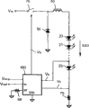
Please refer to Fig. 3, be the circuit diagram of the light emitting diode drive device of suitching type of the present invention.The light emitting diode drive device of suitching type of the present invention uses an energy conversion component 50 coupled in series in light-emitting diode 20~25, and energy conversion component 50 can be a transformer.One switches switch 70 coupled in series in light-emitting diode 20~25 and energy conversion component 50, and diverter switch 70 is used for control flows and crosses the led current I of light-emitting diode 20~25
LEDOne first resistance 75 is coupled to this light-emitting diode 20~25, and this first resistance 75 detects this led current I
LED, export a current signal V
STo a control circuit 100.Control circuit 100 further is coupled to this light-emitting diode 25 to receive a voltage signal V
D, voltage signal V
DBe the forward voltage of light-emitting diode 25.One diode 55 is coupled to energy conversion component 50 and light-emitting diode 20~25.
As current signal V
SBe higher than one first critical value V in the control circuit 100
RThe time, diverter switch 70 is ended, and is limited led current I
LEDLed current I
LEDMaximum can by following formula (2) it:
In the above-mentioned formula (2), L
50The inductance value of expression energy conversion component 50; T
ONThe ON time of expression diverter switch 70; V
F20, V
F21V
F25Be respectively light-emitting diode 20,21 ... 25 forward pressure drop.
When diverter switch 70 was ended, the energy that is stored in energy conversion component 50 can discharge by diode 55 and light-emitting diode 20~25.During the energy discharge of energy conversion component 50, control circuit 100 can detect the value of the forward voltage of this light-emitting diode 25 simultaneously, and according to the characteristic of light-emitting diode 25, forward voltage and its temperature of light-emitting diode 25 are inversely proportional.Therefore, from light-emitting diode 25 detected voltage signal V
DCan learn the temperature of light-emitting diode 25.
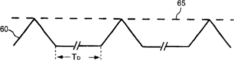
Please refer to Fig. 4 A and Fig. 4 B, be the current waveform schematic diagram of light-emitting diode of the present invention.Wherein, the first critical value V
RMaximum 65 limited led current I
LEDThe peak value of waveform 60.As this current signal V
SLess than one second critical value V
THThe time, diverter switch 70 can through one time of delay T
DAnd be unlocked, in order to set up led current I
LEDThe first critical value V
RMaximum 65 can determine led current I
LEDMean value, therefore, led current I
LEDMean value be controlled, be a fixed value, and can not change along with the inductance value of energy conversion component 50.In addition, time of delay T
DCan adjust, be used for adjusting led current I
LEDAmplitude and the luminosity of light-emitting diode 20~25.
Among the present invention, the first critical value V
RWith voltage signal V
DRespectively with led current I
LEDAnd temperature correlation.The first critical value V
RChange be according to voltage signal V
D, the first critical value V
RChange can compensate the colourity and the lumen degree of light-emitting diode 20~25.In addition, the present invention can further use one second resistance 59 to be coupled to this control circuit 100 in order to adapt to the characteristic of various light-emitting diodes, adjusts slope (slope) in order to determine one, and this adjustment slope is represented the first critical value V
RVariation and this voltage signal V
DThe relativeness of variation.
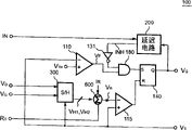
Please refer to Fig. 5, be the circuit diagram of control circuit of the present invention.In control circuit 100, as this current signal V
SGreater than the first critical value V
RThe time, control signal V
GCan be deactivated, thereby this diverter switch 70 is ended.In control circuit 100, as current signal V
SLess than one second critical value V
TH, control signal V then
GCan be by an activation signal V
FActivation, and then control this diverter switch 70 conductings.In control circuit 100, this voltage signal V
DObtain from light-emitting diode 25.
In control circuit 100, a first control circuit include one with door 180, one inverter 131 and a flip-flop 140, first control circuit is according to an inhibit signal INH and this enable signal V
FIn order to export this control signal V
GBe coupled to flip-flop 140 with the output of door 180, and this control signal V
GProduce from the output of flip-flop 140.One second control circuit 115 is coupled to flip-flop 140, as current signal V
SGreater than the first critical value V
RThe time, second control circuit 115 is promptly by flip-flop 140 inactive this control signal V
G
One delay circuit 200 is coupled to and door 180 first input end by inverter 131, and delay circuit 200 is at control signal V
GUnder the dead status, output one has T time of delay
DInhibit signal INH to this and door 180 first input end.So, control signal V
GAt T time of delay
DBe deactivated in during this section.One sample circuit 300 is coupled to this light-emitting diode, and this sample circuit is according to this voltage signal V
D, in order to export one first sampled signal V
H1, one second sampled signal V
H2One matrix current adjustment circuit 600 is coupled to sample circuit 300 and certain electric current I
R, matrix current adjustment circuit 600 receives the first sampled signal V
H1, the second sampled signal V
H2Reach and decide electric current I
R, in order to adjust the first critical value V
RAmplitude.One comparison circuit 110 is coupled to second input with door 180, according to this current signal V
SLess than the second critical value V
TH, in order to output enable signal V
F, this enable signal V
FBe coupled to and door 180 second input, can this control signal of activation V
G
Please refer to Fig. 6, be the circuit diagram of delay circuit of the present invention.In delay circuit 200, one constant current source 250 is coupled to the input IN of control circuit 100, control circuit 100 is coupled to an end of a resistor (not indicating) by this input IN, the other end of this resistor can be couple to a ground connection reference edge, or this input IN also can be coupled to a control voltage V
CNT, can be used for adjusting T time of delay
D, and then the brightness of control light-emitting diode 20~25.
One voltage includes an operational amplifier 210, a resistor 205 and a transistor 220,230,231.Voltage produces a charging current according to the voltage on the resistor that is coupled to input IN on transistor 231.Also use a capacitor 260 to be coupled to a transistor 231 and a transistor 270 in the delay circuit 200, this transistor 270 is controlled by control signal V
GAs control signal V
GStopping using makes when transistor 270 ends, and the charging current that produces on the transistor 231 is immediately to these capacitor 260 chargings, yet when transistor 270 conductings, the voltage on the capacitor 260 promptly discharges by transistor 270.The input of one inverter 280 is coupled to capacitor 260, and inverter 280 produces this inhibit signal INH according to the voltage of setting up on the capacitor 260 in output.
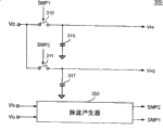
Please refer to Fig. 7, be the circuit diagram of sample circuit of the present invention.In sample circuit 300, a pulse generator 350 is according to control signal V
GStop using and current signal V
SIn order to produce one first pulse wave SMP1 and one second pulse wave SMP2.Cooperate Fig. 8, be the signal waveform schematic diagram of control circuit of the present invention.Wherein, the first pulse wave SMP1 is in control signal V
GAfter stopping using through one first time of delay T
D1And produce, this first time of delay T
D1Can guarantee before the activation first pulse wave SMP1 voltage signal V
DIt is stable state.The second pulse wave SMP2 is at current signal V
SDrop to before the null value and produce, and second time of delay T
D2Can guarantee current signal V
SWhen dropping to before the null value, produce the second pulse wave SMP2.The first pulse wave SMP1 and the second pulse wave SMP2 respectively control its switch 310,311 conducting or end.Diverter switch 310,311 is respectively to voltage signal V
DTake a sample, and on capacitor 315,317, set up the first sampled signal V respectively
H1With the second sampled signal V
H2Therefore, the first sampled signal V
H1With one second sampled signal V
H2,, and represent one first voltage V1 and one second voltage V2 forward forward of light-emitting diode 20~25 respectively according to one first electric current that flows through light-emitting diode 20~25 and one second electric current.
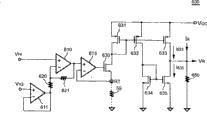
Please refer to Fig. 9, be the circuit diagram of matrix current adjustment circuit of the present invention.In the matrix current adjustment circuit 600, a differential circuit includes operational amplifier 610,611 and resistor 620,621.Differential circuit receives the first sampled signal V
H1With the second sampled signal V
H2, and export a voltage difference at the output of differential circuit.The output of differential circuit is the input that the output of operational amplifier 610 is coupled to an operational amplifier 615.Operational amplifier 615, transistor 630~635 and resistor 650 form another voltage.This another voltage produces electric current I according to the resistance value of the voltage difference and second resistor 59
633, I
635Resistor 650 is coupled to decides electric current I
R, electric current I
633And I
635, and produce the first critical value V
RBy adjusting electric current I
633, I
635Current value can adjust the first critical value V effectively
RValue.
Learn the first sampled signal V according to the above description
H1With one second sampled signal V
H2According to one first electric current that flows through light-emitting diode 20~25 and one second electric current and represent first voltage V1 and the second voltage V2 forward forward of light-emitting diode 20~25 respectively.
First forward voltage V1 and second forward voltage V2 corresponding to the first led current I
1With the second led current I
2, the first led current I
1With the second led current I
2Can get it by following formula (3), (4) respectively:
I
1=I
O×e
V1/VT (3)
I
2=I
O×e
V2/VT (4)
In formula (3), (4), VT can get it by formula (5):
In formula (5), Temp can get it by formula (6):
Above-mentioned formula (3) is in (6), and k is the graceful now constant of Bao Er (Boltzmann ' s constant); Q is an electronic charge; Temp is an absolute temperature; Io is the revers saturation current of diode.
In sum, light emitting diode drive device of the present invention can accurately be obtained the temperature of light-emitting diode 20~25 by voltage signal VD, and utilizes temperature to adjust led current, with the colourity and the lumen degree of compensation light-emitting diode 20~25.
Certainly; the present invention also can have other various embodiments; under the situation that does not deviate from spirit of the present invention and essence thereof; those of ordinary skill in the art work as can make various corresponding changes and distortion according to the present invention, but these corresponding changes and distortion all should belong to the protection range of claim of the present invention.
Claims (11)
1, a kind of light emitting diode drive device is used for driving a light-emitting diode, it is characterized in that, comprising:
One transformer, coupled in series is in this light-emitting diode;
One switches switch, and coupled in series is in this light-emitting diode and this transformer, and this diverter switch is used for controlling a led current;
One first resistance, coupled in series are in this light-emitting diode, and this this led current of first resistance detection is in order to export a current signal;
One control circuit, be coupled to this light-emitting diode, this first resistance and this diverter switch, this control circuit is obtained a voltage signal and is obtained this current signal from this first resistance from this light-emitting diode, arrives this diverter switch according to this voltage signal and this current signal in order to export a control signal;
One diode, coupled in parallel are in this transformer and this light-emitting diode, and this diode discharges in order to the storage power to this transformer by this light-emitting diode; And
One second resistance is coupled to this control circuit, adjusts slope in order to determine one, and this adjustment slope is represented the relativeness of the variation of the variation of one first critical value and this led current;
Wherein, this control signal is controlled this diverter switch and this led current, and when this current signal during greater than this first critical value, this control signal is by this diverter switch, and this first critical value changes along with this voltage signal; When this current signal during less than one second critical value, this control signal is through an adjustable delay after the time, to open this diverter switch conducting.
2, light emitting diode drive device according to claim 1 is characterized in that, this control circuit comprises:
One delay circuit, according to ending of this control signal, in order to export an inhibit signal, this inhibit signal has the adjustable delay time, and wherein, this control signal is to stop using during this section of this adjustable delay time;
One comparison circuit, according to this current signal less than this second critical value, in order to export an activation signal;
One first control circuit is according to this inhibit signal and this enable signal, in order to this control signal of activation;
One second control circuit, according to this current signal greater than this first critical value, in order to stop using this control signal; And
One sample circuit is coupled to this light-emitting diode, and this sample circuit is according to this voltage signal, in order to export one first sampled signal and one second sampled signal;
Wherein, this first sampled signal and this second sampled signal are used for adjusting this first critical value.
3, light emitting diode drive device according to claim 2, it is characterized in that, this first sampled signal and this second sampled signal, according to first electric current of this light-emitting diode and second electric current of light-emitting diode, and represent one first one second voltage forward of voltage and this light-emitting diode forward of this light-emitting diode respectively.
4, a kind of light emitting diode drive device is used for driving a light-emitting diode, it is characterized in that, comprising:
One transformer, coupled in series is in this light-emitting diode;
One switches switch, and coupled in series is in this light-emitting diode and this transformer, and this diverter switch is used for controlling a led current;
One first resistance, coupled in series are in this light-emitting diode, and this this led current of first resistance detection is in order to export a current signal;
One control circuit, be coupled to this light-emitting diode, this first resistance and this diverter switch, this control circuit is obtained a voltage signal and is obtained this current signal from this first resistance from this light-emitting diode, arrives this diverter switch according to this voltage signal and this current signal in order to export a control signal; And
One diode, coupled in parallel are in this transformer and this light-emitting diode, and this diode discharges in order to the storage power to this transformer by this light-emitting diode;
Wherein, this control signal is controlled this diverter switch and this led current, and when this current signal during greater than one first critical value, this control signal is by this diverter switch; When this current signal during less than one second critical value, this control signal is opened this diverter switch conducting.
5, light emitting diode drive device according to claim 4 is characterized in that, this first critical value is along with this voltage signal changes.
6, light emitting diode drive device according to claim 4 is characterized in that, this control circuit comprises:
One delay circuit, according to ending of this control signal, in order to export an inhibit signal, this inhibit signal has the adjustable delay time;
One comparison circuit, according to this current signal less than this second critical value, in order to export an activation signal;
One first control circuit is according to this inhibit signal and this enable signal, in order to this control signal of activation;
One second control circuit, according to this current signal greater than this first critical value, in order to stop using this control signal; And
One sample circuit is coupled to this light-emitting diode, and this sample circuit is according to this voltage signal, in order to export one first sampled signal and one second sampled signal;
Wherein, this first sampled signal and this second sampled signal are used for adjusting this first critical value.
7, light emitting diode drive device according to claim 6, it is characterized in that, this first sampled signal and this second sampled signal, according to first electric current of this light-emitting diode and second electric current of this light-emitting diode, and represent one first voltage and one second voltage forward forward of this light-emitting diode respectively.
8, a kind of light emitting diode drive device is used for driving a light-emitting diode, it is characterized in that, comprising:
One transformer, coupled in series is in this light-emitting diode;
One switches switch, and coupled in series is in this light-emitting diode and this transformer, and this diverter switch is used for controlling a led current;
One control circuit is coupled to this light-emitting diode, obtains a voltage signal from this light-emitting diode, and this control circuit is according to this voltage signal and this led current, to export a control signal; And
One diode, coupled in parallel are in this transformer and this light-emitting diode, and this diode discharges in order to the storage power to this transformer by this light-emitting diode;
Wherein, this control signal is controlled this diverter switch and this led current, and this led current produces a current signal by a resistance, and when this led current during greater than one first critical value, this control signal is by this diverter switch.
9, light emitting diode drive device according to claim 8 is characterized in that, this first critical value is along with this voltage signal changes.
10, light emitting diode drive device according to claim 8 is characterized in that, this control circuit comprises:
One delay circuit, according to ending of this control signal, in order to export an inhibit signal, this inhibit signal has the adjustable delay time;
One comparison circuit, according to this current signal less than this second critical value, in order to export an activation signal;
One first control circuit is according to this inhibit signal and this enable signal, in order to this control signal of activation;
One second control circuit, according to this current signal greater than this first critical value, in order to stop using this control signal; And
One sample circuit is coupled to this light-emitting diode, and this sample circuit is according to this voltage signal, in order to export one first sampled signal and one second sampled signal;
Wherein, this first sampled signal and this second sampled signal are used for adjusting the variation of this first critical value.
11, light emitting diode drive device according to claim 10, it is characterized in that, this first sampled signal and this second sampled signal, according to first electric current of this light-emitting diode and second electric current of this light-emitting diode, and represent one first voltage and one second voltage forward forward of this light-emitting diode respectively.
Priority Applications (1)
| Application Number | Priority Date | Filing Date | Title |
|---|---|---|---|
| CNB2005100230644A CN100531487C (en) | 2005-12-28 | 2005-12-28 | LED driving device |
Applications Claiming Priority (1)
| Application Number | Priority Date | Filing Date | Title |
|---|---|---|---|
| CNB2005100230644A CN100531487C (en) | 2005-12-28 | 2005-12-28 | LED driving device |
Publications (2)
| Publication Number | Publication Date |
|---|---|
| CN1993005A CN1993005A (en) | 2007-07-04 |
| CN100531487C true CN100531487C (en) | 2009-08-19 |
Family
ID=38214848
Family Applications (1)
| Application Number | Title | Priority Date | Filing Date |
|---|---|---|---|
| CNB2005100230644A Expired - Fee Related CN100531487C (en) | 2005-12-28 | 2005-12-28 | LED driving device |
Country Status (1)
| Country | Link |
|---|---|
| CN (1) | CN100531487C (en) |
Families Citing this family (3)
| Publication number | Priority date | Publication date | Assignee | Title |
|---|---|---|---|---|
| JP4452306B2 (en) * | 2007-12-26 | 2010-04-21 | シャープ株式会社 | Pulse signal delay circuit and LED drive circuit |
| CN101505558B (en) * | 2008-02-04 | 2012-06-13 | 通嘉科技股份有限公司 | Light emission element driving circuit having compensation mechanism |
| JP2012054461A (en) * | 2010-09-02 | 2012-03-15 | Sanken Electric Co Ltd | Led drive circuit |
-
2005
- 2005-12-28 CN CNB2005100230644A patent/CN100531487C/en not_active Expired - Fee Related
Also Published As
| Publication number | Publication date |
|---|---|
| CN1993005A (en) | 2007-07-04 |
Similar Documents
| Publication | Publication Date | Title |
|---|---|---|
| US7259525B2 (en) | High efficiency switching LED driver | |
| CN101489335B (en) | LED driving circuit and secondary side controller thereof | |
| CN101707837B (en) | LED drive circuit of source driver with change of output voltage and induction quantity keeping constant current | |
| CN101742771B (en) | Portable type lamp, light dimming circuit and light dimming method | |
| CN102076149B (en) | Light source drive circuit, controller and method for controlling light source brightness | |
| CN101489342A (en) | LED driver circuit and driving method thereof | |
| US20100033146A1 (en) | Current sensing for high voltage buck converter | |
| CN101527990B (en) | Light emitting diode driving circuit | |
| CN101505561A (en) | Control circuit for led drive and its off-line control circuit | |
| CN102340911A (en) | Control circuit and control method for light emitting diode (LED) driver | |
| CN100566482C (en) | Light emitting diode drive device | |
| CN101155449A (en) | Width pulse modulation device and its control circuit and method and method | |
| CN103957648B (en) | Controllable silicon, simulation, PWM light modulation universal circuit and LED drive chip | |
| CN110446308A (en) | For controlling control circuit, driving circuit, LED lamp system and the control method of power transistor | |
| CN100531487C (en) | LED driving device | |
| CN202587506U (en) | Adjustable constant current source | |
| CN202310230U (en) | Energy saving light box control circuit and energy saving light box | |
| CN102487567A (en) | LED constant current drive circuit used for portable device | |
| CN101511141B (en) | Control technique for switch power supply, inductance and current | |
| CN102111929A (en) | Circuit for controlling CC (Constant Current) driving and dimming of LED | |
| CN104283422A (en) | Boosting converting circuit and drive control module thereof | |
| CN201360369Y (en) | LED driver circuit | |
| CN109185212B (en) | Speed regulating circuit of direct current fan | |
| CN102223743B (en) | Light emitting diode (LED) driving control circuit and method thereof | |
| CN201731275U (en) | Intelligent light-adjusting flashlight capable of adjusting light intensity |
Legal Events
| Date | Code | Title | Description |
|---|---|---|---|
| C06 | Publication | ||
| PB01 | Publication | ||
| C10 | Entry into substantive examination | ||
| SE01 | Entry into force of request for substantive examination | ||
| C14 | Grant of patent or utility model | ||
| GR01 | Patent grant | ||
| CF01 | Termination of patent right due to non-payment of annual fee |
Granted publication date: 20090819 Termination date: 20201228 |
|
| CF01 | Termination of patent right due to non-payment of annual fee |