CN100537232C - Process for forming a patterned thin film structure for in-mold decoration - Google Patents
Process for forming a patterned thin film structure for in-mold decoration Download PDFInfo
- Publication number
- CN100537232C CN100537232C CN200410048743.2A CN200410048743A CN100537232C CN 100537232 C CN100537232 C CN 100537232C CN 200410048743 A CN200410048743 A CN 200410048743A CN 100537232 C CN100537232 C CN 100537232C
- Authority
- CN
- China
- Prior art keywords
- substrate
- membrane structure
- film
- forms
- peelable
- Prior art date
- Legal status (The legal status is an assumption and is not a legal conclusion. Google has not performed a legal analysis and makes no representation as to the accuracy of the status listed.)
- Expired - Fee Related
Links
Images


Classifications
-
- H—ELECTRICITY
- H05—ELECTRIC TECHNIQUES NOT OTHERWISE PROVIDED FOR
- H05K—PRINTED CIRCUITS; CASINGS OR CONSTRUCTIONAL DETAILS OF ELECTRIC APPARATUS; MANUFACTURE OF ASSEMBLAGES OF ELECTRICAL COMPONENTS
- H05K3/00—Apparatus or processes for manufacturing printed circuits
- H05K3/02—Apparatus or processes for manufacturing printed circuits in which the conductive material is applied to the surface of the insulating support and is thereafter removed from such areas of the surface which are not intended for current conducting or shielding
- H05K3/04—Apparatus or processes for manufacturing printed circuits in which the conductive material is applied to the surface of the insulating support and is thereafter removed from such areas of the surface which are not intended for current conducting or shielding the conductive material being removed mechanically, e.g. by punching
- H05K3/046—Apparatus or processes for manufacturing printed circuits in which the conductive material is applied to the surface of the insulating support and is thereafter removed from such areas of the surface which are not intended for current conducting or shielding the conductive material being removed mechanically, e.g. by punching by selective transfer or selective detachment of a conductive layer
- H05K3/048—Apparatus or processes for manufacturing printed circuits in which the conductive material is applied to the surface of the insulating support and is thereafter removed from such areas of the surface which are not intended for current conducting or shielding the conductive material being removed mechanically, e.g. by punching by selective transfer or selective detachment of a conductive layer using a lift-off resist pattern or a release layer pattern
-
- B—PERFORMING OPERATIONS; TRANSPORTING
- B32—LAYERED PRODUCTS
- B32B—LAYERED PRODUCTS, i.e. PRODUCTS BUILT-UP OF STRATA OF FLAT OR NON-FLAT, e.g. CELLULAR OR HONEYCOMB, FORM
- B32B38/00—Ancillary operations in connection with laminating processes
- B32B38/10—Removing layers, or parts of layers, mechanically or chemically
-
- C—CHEMISTRY; METALLURGY
- C23—COATING METALLIC MATERIAL; COATING MATERIAL WITH METALLIC MATERIAL; CHEMICAL SURFACE TREATMENT; DIFFUSION TREATMENT OF METALLIC MATERIAL; COATING BY VACUUM EVAPORATION, BY SPUTTERING, BY ION IMPLANTATION OR BY CHEMICAL VAPOUR DEPOSITION, IN GENERAL; INHIBITING CORROSION OF METALLIC MATERIAL OR INCRUSTATION IN GENERAL
- C23C—COATING METALLIC MATERIAL; COATING MATERIAL WITH METALLIC MATERIAL; SURFACE TREATMENT OF METALLIC MATERIAL BY DIFFUSION INTO THE SURFACE, BY CHEMICAL CONVERSION OR SUBSTITUTION; COATING BY VACUUM EVAPORATION, BY SPUTTERING, BY ION IMPLANTATION OR BY CHEMICAL VAPOUR DEPOSITION, IN GENERAL
- C23C14/00—Coating by vacuum evaporation, by sputtering or by ion implantation of the coating forming material
- C23C14/04—Coating on selected surface areas, e.g. using masks
- C23C14/042—Coating on selected surface areas, e.g. using masks using masks
-
- C—CHEMISTRY; METALLURGY
- C23—COATING METALLIC MATERIAL; COATING MATERIAL WITH METALLIC MATERIAL; CHEMICAL SURFACE TREATMENT; DIFFUSION TREATMENT OF METALLIC MATERIAL; COATING BY VACUUM EVAPORATION, BY SPUTTERING, BY ION IMPLANTATION OR BY CHEMICAL VAPOUR DEPOSITION, IN GENERAL; INHIBITING CORROSION OF METALLIC MATERIAL OR INCRUSTATION IN GENERAL
- C23C—COATING METALLIC MATERIAL; COATING MATERIAL WITH METALLIC MATERIAL; SURFACE TREATMENT OF METALLIC MATERIAL BY DIFFUSION INTO THE SURFACE, BY CHEMICAL CONVERSION OR SUBSTITUTION; COATING BY VACUUM EVAPORATION, BY SPUTTERING, BY ION IMPLANTATION OR BY CHEMICAL VAPOUR DEPOSITION, IN GENERAL
- C23C14/00—Coating by vacuum evaporation, by sputtering or by ion implantation of the coating forming material
- C23C14/06—Coating by vacuum evaporation, by sputtering or by ion implantation of the coating forming material characterised by the coating material
- C23C14/08—Oxides
- C23C14/086—Oxides of zinc, germanium, cadmium, indium, tin, thallium or bismuth
-
- C—CHEMISTRY; METALLURGY
- C23—COATING METALLIC MATERIAL; COATING MATERIAL WITH METALLIC MATERIAL; CHEMICAL SURFACE TREATMENT; DIFFUSION TREATMENT OF METALLIC MATERIAL; COATING BY VACUUM EVAPORATION, BY SPUTTERING, BY ION IMPLANTATION OR BY CHEMICAL VAPOUR DEPOSITION, IN GENERAL; INHIBITING CORROSION OF METALLIC MATERIAL OR INCRUSTATION IN GENERAL
- C23C—COATING METALLIC MATERIAL; COATING MATERIAL WITH METALLIC MATERIAL; SURFACE TREATMENT OF METALLIC MATERIAL BY DIFFUSION INTO THE SURFACE, BY CHEMICAL CONVERSION OR SUBSTITUTION; COATING BY VACUUM EVAPORATION, BY SPUTTERING, BY ION IMPLANTATION OR BY CHEMICAL VAPOUR DEPOSITION, IN GENERAL
- C23C14/00—Coating by vacuum evaporation, by sputtering or by ion implantation of the coating forming material
- C23C14/06—Coating by vacuum evaporation, by sputtering or by ion implantation of the coating forming material characterised by the coating material
- C23C14/14—Metallic material, boron or silicon
- C23C14/20—Metallic material, boron or silicon on organic substrates
-
- G—PHYSICS
- G02—OPTICS
- G02F—OPTICAL DEVICES OR ARRANGEMENTS FOR THE CONTROL OF LIGHT BY MODIFICATION OF THE OPTICAL PROPERTIES OF THE MEDIA OF THE ELEMENTS INVOLVED THEREIN; NON-LINEAR OPTICS; FREQUENCY-CHANGING OF LIGHT; OPTICAL LOGIC ELEMENTS; OPTICAL ANALOGUE/DIGITAL CONVERTERS
- G02F1/00—Devices or arrangements for the control of the intensity, colour, phase, polarisation or direction of light arriving from an independent light source, e.g. switching, gating or modulating; Non-linear optics
- G02F1/01—Devices or arrangements for the control of the intensity, colour, phase, polarisation or direction of light arriving from an independent light source, e.g. switching, gating or modulating; Non-linear optics for the control of the intensity, phase, polarisation or colour
- G02F1/13—Devices or arrangements for the control of the intensity, colour, phase, polarisation or direction of light arriving from an independent light source, e.g. switching, gating or modulating; Non-linear optics for the control of the intensity, phase, polarisation or colour based on liquid crystals, e.g. single liquid crystal display cells
- G02F1/133—Constructional arrangements; Operation of liquid crystal cells; Circuit arrangements
- G02F1/1333—Constructional arrangements; Manufacturing methods
- G02F1/1343—Electrodes
- G02F1/13439—Electrodes characterised by their electrical, optical, physical properties; materials therefor; method of making
-
- G—PHYSICS
- G09—EDUCATION; CRYPTOGRAPHY; DISPLAY; ADVERTISING; SEALS
- G09F—DISPLAYING; ADVERTISING; SIGNS; LABELS OR NAME-PLATES; SEALS
- G09F7/00—Signs, name or number plates, letters, numerals, or symbols; Panels or boards
- G09F7/16—Letters, numerals, or other symbols adapted for permanent fixing to a support
- G09F7/165—Letters, numerals, or other symbols adapted for permanent fixing to a support obtained by a treatment of the support
-
- H—ELECTRICITY
- H05—ELECTRIC TECHNIQUES NOT OTHERWISE PROVIDED FOR
- H05K—PRINTED CIRCUITS; CASINGS OR CONSTRUCTIONAL DETAILS OF ELECTRIC APPARATUS; MANUFACTURE OF ASSEMBLAGES OF ELECTRICAL COMPONENTS
- H05K3/00—Apparatus or processes for manufacturing printed circuits
- H05K3/02—Apparatus or processes for manufacturing printed circuits in which the conductive material is applied to the surface of the insulating support and is thereafter removed from such areas of the surface which are not intended for current conducting or shielding
- H05K3/04—Apparatus or processes for manufacturing printed circuits in which the conductive material is applied to the surface of the insulating support and is thereafter removed from such areas of the surface which are not intended for current conducting or shielding the conductive material being removed mechanically, e.g. by punching
-
- H—ELECTRICITY
- H05—ELECTRIC TECHNIQUES NOT OTHERWISE PROVIDED FOR
- H05K—PRINTED CIRCUITS; CASINGS OR CONSTRUCTIONAL DETAILS OF ELECTRIC APPARATUS; MANUFACTURE OF ASSEMBLAGES OF ELECTRICAL COMPONENTS
- H05K3/00—Apparatus or processes for manufacturing printed circuits
- H05K3/38—Improvement of the adhesion between the insulating substrate and the metal
- H05K3/386—Improvement of the adhesion between the insulating substrate and the metal by the use of an organic polymeric bonding layer, e.g. adhesive
-
- B—PERFORMING OPERATIONS; TRANSPORTING
- B29—WORKING OF PLASTICS; WORKING OF SUBSTANCES IN A PLASTIC STATE IN GENERAL
- B29C—SHAPING OR JOINING OF PLASTICS; SHAPING OF MATERIAL IN A PLASTIC STATE, NOT OTHERWISE PROVIDED FOR; AFTER-TREATMENT OF THE SHAPED PRODUCTS, e.g. REPAIRING
- B29C45/00—Injection moulding, i.e. forcing the required volume of moulding material through a nozzle into a closed mould; Apparatus therefor
- B29C45/14—Injection moulding, i.e. forcing the required volume of moulding material through a nozzle into a closed mould; Apparatus therefor incorporating preformed parts or layers, e.g. injection moulding around inserts or for coating articles
- B29C45/14778—Injection moulding, i.e. forcing the required volume of moulding material through a nozzle into a closed mould; Apparatus therefor incorporating preformed parts or layers, e.g. injection moulding around inserts or for coating articles the article consisting of a material with particular properties, e.g. porous, brittle
- B29C45/14811—Multilayered articles
-
- B—PERFORMING OPERATIONS; TRANSPORTING
- B29—WORKING OF PLASTICS; WORKING OF SUBSTANCES IN A PLASTIC STATE IN GENERAL
- B29K—INDEXING SCHEME ASSOCIATED WITH SUBCLASSES B29B, B29C OR B29D, RELATING TO MOULDING MATERIALS OR TO MATERIALS FOR MOULDS, REINFORCEMENTS, FILLERS OR PREFORMED PARTS, e.g. INSERTS
- B29K2995/00—Properties of moulding materials, reinforcements, fillers, preformed parts or moulds
- B29K2995/0018—Properties of moulding materials, reinforcements, fillers, preformed parts or moulds having particular optical properties, e.g. fluorescent or phosphorescent
- B29K2995/002—Coloured
-
- H—ELECTRICITY
- H05—ELECTRIC TECHNIQUES NOT OTHERWISE PROVIDED FOR
- H05K—PRINTED CIRCUITS; CASINGS OR CONSTRUCTIONAL DETAILS OF ELECTRIC APPARATUS; MANUFACTURE OF ASSEMBLAGES OF ELECTRICAL COMPONENTS
- H05K2201/00—Indexing scheme relating to printed circuits covered by H05K1/00
- H05K2201/03—Conductive materials
- H05K2201/0302—Properties and characteristics in general
- H05K2201/0317—Thin film conductor layer; Thin film passive component
-
- H—ELECTRICITY
- H05—ELECTRIC TECHNIQUES NOT OTHERWISE PROVIDED FOR
- H05K—PRINTED CIRCUITS; CASINGS OR CONSTRUCTIONAL DETAILS OF ELECTRIC APPARATUS; MANUFACTURE OF ASSEMBLAGES OF ELECTRICAL COMPONENTS
- H05K2203/00—Indexing scheme relating to apparatus or processes for manufacturing printed circuits covered by H05K3/00
- H05K2203/02—Details related to mechanical or acoustic processing, e.g. drilling, punching, cutting, using ultrasound
- H05K2203/0257—Brushing, e.g. cleaning the conductive pattern by brushing or wiping
-
- H—ELECTRICITY
- H05—ELECTRIC TECHNIQUES NOT OTHERWISE PROVIDED FOR
- H05K—PRINTED CIRCUITS; CASINGS OR CONSTRUCTIONAL DETAILS OF ELECTRIC APPARATUS; MANUFACTURE OF ASSEMBLAGES OF ELECTRICAL COMPONENTS
- H05K2203/00—Indexing scheme relating to apparatus or processes for manufacturing printed circuits covered by H05K3/00
- H05K2203/02—Details related to mechanical or acoustic processing, e.g. drilling, punching, cutting, using ultrasound
- H05K2203/0264—Peeling insulating layer, e.g. foil, or separating mask
-
- H—ELECTRICITY
- H05—ELECTRIC TECHNIQUES NOT OTHERWISE PROVIDED FOR
- H05K—PRINTED CIRCUITS; CASINGS OR CONSTRUCTIONAL DETAILS OF ELECTRIC APPARATUS; MANUFACTURE OF ASSEMBLAGES OF ELECTRICAL COMPONENTS
- H05K2203/00—Indexing scheme relating to apparatus or processes for manufacturing printed circuits covered by H05K3/00
- H05K2203/05—Patterning and lithography; Masks; Details of resist
- H05K2203/0502—Patterning and lithography
- H05K2203/0522—Using an adhesive pattern
-
- H—ELECTRICITY
- H05—ELECTRIC TECHNIQUES NOT OTHERWISE PROVIDED FOR
- H05K—PRINTED CIRCUITS; CASINGS OR CONSTRUCTIONAL DETAILS OF ELECTRIC APPARATUS; MANUFACTURE OF ASSEMBLAGES OF ELECTRICAL COMPONENTS
- H05K2203/00—Indexing scheme relating to apparatus or processes for manufacturing printed circuits covered by H05K3/00
- H05K2203/07—Treatments involving liquids, e.g. plating, rinsing
- H05K2203/0736—Methods for applying liquids, e.g. spraying
- H05K2203/0746—Local treatment using a fluid jet, e.g. for removing or cleaning material; Providing mechanical pressure using a fluid jet
-
- H—ELECTRICITY
- H05—ELECTRIC TECHNIQUES NOT OTHERWISE PROVIDED FOR
- H05K—PRINTED CIRCUITS; CASINGS OR CONSTRUCTIONAL DETAILS OF ELECTRIC APPARATUS; MANUFACTURE OF ASSEMBLAGES OF ELECTRICAL COMPONENTS
- H05K3/00—Apparatus or processes for manufacturing printed circuits
- H05K3/10—Apparatus or processes for manufacturing printed circuits in which conductive material is applied to the insulating support in such a manner as to form the desired conductive pattern
- H05K3/14—Apparatus or processes for manufacturing printed circuits in which conductive material is applied to the insulating support in such a manner as to form the desired conductive pattern using spraying techniques to apply the conductive material, e.g. vapour evaporation
- H05K3/146—By vapour deposition
-
- H—ELECTRICITY
- H05—ELECTRIC TECHNIQUES NOT OTHERWISE PROVIDED FOR
- H05K—PRINTED CIRCUITS; CASINGS OR CONSTRUCTIONAL DETAILS OF ELECTRIC APPARATUS; MANUFACTURE OF ASSEMBLAGES OF ELECTRICAL COMPONENTS
- H05K3/00—Apparatus or processes for manufacturing printed circuits
- H05K3/10—Apparatus or processes for manufacturing printed circuits in which conductive material is applied to the insulating support in such a manner as to form the desired conductive pattern
- H05K3/14—Apparatus or processes for manufacturing printed circuits in which conductive material is applied to the insulating support in such a manner as to form the desired conductive pattern using spraying techniques to apply the conductive material, e.g. vapour evaporation
- H05K3/16—Apparatus or processes for manufacturing printed circuits in which conductive material is applied to the insulating support in such a manner as to form the desired conductive pattern using spraying techniques to apply the conductive material, e.g. vapour evaporation by cathodic sputtering
-
- H—ELECTRICITY
- H05—ELECTRIC TECHNIQUES NOT OTHERWISE PROVIDED FOR
- H05K—PRINTED CIRCUITS; CASINGS OR CONSTRUCTIONAL DETAILS OF ELECTRIC APPARATUS; MANUFACTURE OF ASSEMBLAGES OF ELECTRICAL COMPONENTS
- H05K3/00—Apparatus or processes for manufacturing printed circuits
- H05K3/10—Apparatus or processes for manufacturing printed circuits in which conductive material is applied to the insulating support in such a manner as to form the desired conductive pattern
- H05K3/18—Apparatus or processes for manufacturing printed circuits in which conductive material is applied to the insulating support in such a manner as to form the desired conductive pattern using precipitation techniques to apply the conductive material
- H05K3/181—Apparatus or processes for manufacturing printed circuits in which conductive material is applied to the insulating support in such a manner as to form the desired conductive pattern using precipitation techniques to apply the conductive material by electroless plating
- H05K3/182—Apparatus or processes for manufacturing printed circuits in which conductive material is applied to the insulating support in such a manner as to form the desired conductive pattern using precipitation techniques to apply the conductive material by electroless plating characterised by the patterning method
- H05K3/184—Apparatus or processes for manufacturing printed circuits in which conductive material is applied to the insulating support in such a manner as to form the desired conductive pattern using precipitation techniques to apply the conductive material by electroless plating characterised by the patterning method using masks
-
- H—ELECTRICITY
- H10—SEMICONDUCTOR DEVICES; ELECTRIC SOLID-STATE DEVICES NOT OTHERWISE PROVIDED FOR
- H10K—ORGANIC ELECTRIC SOLID-STATE DEVICES
- H10K71/00—Manufacture or treatment specially adapted for the organic devices covered by this subclass
- H10K71/60—Forming conductive regions or layers, e.g. electrodes
- H10K71/611—Forming conductive regions or layers, e.g. electrodes using printing deposition, e.g. ink jet printing
-
- Y—GENERAL TAGGING OF NEW TECHNOLOGICAL DEVELOPMENTS; GENERAL TAGGING OF CROSS-SECTIONAL TECHNOLOGIES SPANNING OVER SEVERAL SECTIONS OF THE IPC; TECHNICAL SUBJECTS COVERED BY FORMER USPC CROSS-REFERENCE ART COLLECTIONS [XRACs] AND DIGESTS
- Y10—TECHNICAL SUBJECTS COVERED BY FORMER USPC
- Y10S—TECHNICAL SUBJECTS COVERED BY FORMER USPC CROSS-REFERENCE ART COLLECTIONS [XRACs] AND DIGESTS
- Y10S156/00—Adhesive bonding and miscellaneous chemical manufacture
- Y10S156/918—Delaminating processes adapted for specified product, e.g. delaminating medical specimen slide
- Y10S156/919—Delaminating in preparation for post processing recycling step
- Y10S156/922—Specified electronic component delaminating in preparation for recycling
-
- Y—GENERAL TAGGING OF NEW TECHNOLOGICAL DEVELOPMENTS; GENERAL TAGGING OF CROSS-SECTIONAL TECHNOLOGIES SPANNING OVER SEVERAL SECTIONS OF THE IPC; TECHNICAL SUBJECTS COVERED BY FORMER USPC CROSS-REFERENCE ART COLLECTIONS [XRACs] AND DIGESTS
- Y10—TECHNICAL SUBJECTS COVERED BY FORMER USPC
- Y10T—TECHNICAL SUBJECTS COVERED BY FORMER US CLASSIFICATION
- Y10T156/00—Adhesive bonding and miscellaneous chemical manufacture
- Y10T156/11—Methods of delaminating, per se; i.e., separating at bonding face
- Y10T156/1168—Gripping and pulling work apart during delaminating
- Y10T156/1189—Gripping and pulling work apart during delaminating with shearing during delaminating
Landscapes
- Engineering & Computer Science (AREA)
- Chemical & Material Sciences (AREA)
- Physics & Mathematics (AREA)
- Mechanical Engineering (AREA)
- Manufacturing & Machinery (AREA)
- Microelectronics & Electronic Packaging (AREA)
- Chemical Kinetics & Catalysis (AREA)
- Materials Engineering (AREA)
- Metallurgy (AREA)
- Organic Chemistry (AREA)
- General Physics & Mathematics (AREA)
- Nonlinear Science (AREA)
- Theoretical Computer Science (AREA)
- Mathematical Physics (AREA)
- Crystallography & Structural Chemistry (AREA)
- Optics & Photonics (AREA)
- Laminated Bodies (AREA)
- Moulds For Moulding Plastics Or The Like (AREA)
- Injection Moulding Of Plastics Or The Like (AREA)
- Manufacturing Of Printed Circuit Boards (AREA)
Abstract
A process for forming a patterned thin film structure on a substrate or in-mold decoration film is disclosed. A pattern is printed with a material, such as a masking coating or ink, on the substrate, the pattern being such that, in one embodiment, the desired structures will be formed in the areas where the printed material is not present, i.e., a negative image of thin film structure to be formed is printed. In another embodiment, the pattern is printed with a material that is difficult to strip from the substrate, and the desired thin film structures will be formed in the areas where the printed material is present, i.e., a positive image of the thin film structure is printed. The thin film material is deposited on the patterned substrate, and the undesired area is stripped, leaving behind the patterned thin film structure.
Description
Technical field
Present invention relates in general to in-mold decoration.The present invention discloses a kind of in the method that is used for forming on the substrate of in-mold decoration patterned film.
Background technology
In-mold decoration (IMD) has formed the technology of a cover decoration injecting molded part of popularizing day by day.The IMD technology is to be used for text, numeral, legend, other symbol and information and mere decoration design are joined injecting molded part, as phone and other consumer-elcetronics devices, fascia, the container that is used for the consumer goods and packaging material and the whole field of injecting molded part in fact.
IMD is usually directed to form in-mold decoration film (IMD film or IMD decorating film), and it comprises the image that will be transferred to or be incorporated into the surface of injecting molded part.In a typical inner mould transfer printing method, PETG (PET) film is handled (to promote the image transfer printing) with releasing agent, be coated with then with durable layer so that oil resistivity and resistance to scraping to be provided.Printing and/or form with other method is decorated on the PET film of treated and coating then, then is coated with this film with formation in-mold transfer printing film with adhesive (for example, hot-melt adhesive or polyurethane binder).Before injecting molten resin, this film is embedded injection molding then, and will decorate (or other image) and be transferred to injection-molded article from the PET film.In typical molding embedding grammar, this decoration or other image are not to be transferred to injection-molded article from the IMD decorating film, but the film that IMD is decorated is bonded in injection-molded article and becomes its part.In a typical molding embedding grammar, used Merlon (PC) substrate.Be included in the decoration on the injection-molded article or other image is printed or be formed at other method on the surface of PC substrate.This patterned substrate coating provides IMD decorating film with thin protective layer (so that protection printing ink is avoided damage in injection process) then.
In some cases, the IMD technology decoration or other image that can be used to comprise pattern metal film or other thin-film material is applied to or joins injection-molded article.In one approach, this patterned film design adds by form the pattern metal thin layer on the IMD decorating film.The method of prior art that a kind of typical manufacturing comprises the in-mold decoration film of pattern metal film relates to uses photoetching technique and chemical etching.Typical photoetching method comprises a plurality of time-consuming and expensive steps, comprises that (1) forms non-pattern metal thin layer; (2) with this metallic film of photic resist-coating; (3) come patterned in (for example) ultraviolet ray the photoresist graph exposure by photomask; (4) by removing the image " development " that photoresist (type that depends on used photoresist) makes patterning, so that at zone (that is the zone of thin-film material, is not set) exposing metal film that metallic film will be removed from exposure or unexposed area; (5) utilize chemical etching method so that remove this film from the zone that photoresist has been removed; And (6) remove remaining photoresist so that expose the membrane structure of patterning.
Some processing step in the photoetching method as graph exposure, is time-consuming also the needs carefully with mask and mobile target area registration and aligning.In addition, developing and remove photoresist and handle refuse from chemical etching technology, except causing environmental hazard potentially, may be time-consuming and expensive.Chemical etching method also often causes the less surface of gloss, and this does not normally meet for high-end decorative applications and needs.
Therefore, need a kind of method that is used for forming as the patterned film structure of IMD decorating film on the plasticity substrate, it need not to use photoetching process or chemical etching.
Summary of the invention
The invention provides a kind of method that on substrate, forms the patterned film structure, may further comprise the steps: utilize the peelable material printed patterns on substrate that comprises the redispersible particle of calculating by weight 5-80%, the peelable material of printing limits the zone that membrane structure will form on substrate, it is the negative-appearing image that uses the decoration design that thin-film material will form by comprising on substrate, so that the peelable material of printing is present in the inchoate zone of on-chip membrane structure and the peelable material of printing is not present in the zone that on-chip membrane structure will form basically; The film of deposition materials on pattern structure; And peel off peelable material from substrate; Any thin-film material of peelable material and formation thereon is removed by peeling off thus, stays the membrane structure that forms on substrate with the shape of decorating design; And wherein this substrate and the patterned film design that forms thereon are suitable for as in-mold decoration (IMD) decorating film.
Peelable material comprises the redispersible particle of calculating by weight 10-60%.
Peelable material comprise water-soluble or aqueous dispersion polymers as adhesive.
Water-soluble or aqueous dispersion polymers is to be selected from by polyvinyl alcohol, polyvinylpyrrolidone, polyvinyl pyridine, polyacrylic acid, polymethylacrylic acid, polyacrylamide, polyethylene glycol, ethene-maleic anhydride copolymers, vinyl ethers-maleic anhydride copolymers, styrene-maleic anhydride copolymers, butylene-itaconic acid copolymer, PEO, polystyrolsulfon acid ester, such as hydroxyethylcellulose, hydroxypropyl cellulose, methylcellulose, the such cellulose derivative of carboxymethyl cellulose, xanthans, gum arabic, gelatin, lecithin, with and the group formed of copolymer.
Water-soluble or aqueous dispersion polymers comprises aqueous dispersion polymers, is selected from the group of being made up of the dispersed wax of water dispersible or alkali, polyolefin or acrylic based emulsion or dispersion.
Peelable material comprises that dissolution with solvents or solvent polymer dispersion are as adhesive.
The redispersible particle is derived from silica, CaCO
3, CaSO
4, BaSO
4, Al
2O
3, TiO
2, hollow spheres, non-film forming latex or dispersion, inorganic pigment or organic pigment.
Particle is polymer particles or polymer composite particles.
Peelable material comprises an additive, is selected from the group of being made up of surfactant, dyestuff, curing agent and plasticizer; Thereby the existence of additive promotes to peel off peelable material after depositing of thin film.
Strip step comprises uses solvent to remove peelable material.
Solvent be select Free water, the aqueous solution, alcohol, ketone, ester, ether, acid amides, hydrocarbon, alkylbenzene, pyrrolidones, sulfone, dimethyl sulfoxide (DMSO), with and composition thereof the group formed with derivative.
Thin-film material can be non-conductive.
Thin-film material can be semi-conductive.
Thin-film material can conduct electricity.
Conductive film material be selected from by metal, metal oxide, with and the material of the group formed of alloy and multilayer materials.
Conductive material is a metal, is selected from the group of being made up of aluminium, copper, zinc, tin, molybdenum, nickel, chromium, silver, gold, iron, indium, thallium, titanium, tantalum, tungsten, rhodium, palladium, platinum and cobalt.
Conductive material is metal oxide or sulfide, is selected from by the indium oxide of tin indium oxide (ITO), indium zinc oxide (IZO), aluminum zinc oxide, gadolinium oxide indium, tin oxide, doped with fluorine or the group that zinc sulphide is formed.
The step of deposit film can comprise spraying plating.
The step of deposit film can comprise vapour deposition.
The step of deposit film can comprise vacuum deposition.
The step of deposit film can comprise plating.
The step of deposit film can comprise electroless plating.
The step of deposit film can comprise electroforming.
Print steps can comprise hectographic printing.
Print steps can comprise driography.
Print steps can comprise electrophotographic printing.
Print steps can comprise litho.
Print steps can comprise photogravure.
Print steps can comprise the temperature-sensitive printing.
Print steps can comprise ink jet printing.
Print steps can comprise serigraphy.
Print steps can comprise letterpress.
Substrate can comprise the plasticity substrate.The plasticity substrate comprises part plasticity substrate roller.
In addition, the method for formation patterned film structure is the part of roll-to-roll (roll-to-roll) technology of preparation in-mold decoration film on substrate.
Substrate comprises PETG (PET) film.
According to the method that on substrate, forms the patterned film structure of the present invention, further be included in and carry out following step on the substrate before the formation patterned film structure: handle or coating PET film with releasing agent or coating; And with durable layer coating treated or through the PET film of coating so that oil resistivity and resistance to scraping to be provided.
According to the method that on substrate, forms the patterned film structure of the present invention, use second of the printing material printing that is different from thin-film material to decorate design on the substrate but further be included in.
According to the method that on substrate, forms the patterned film structure of the present invention, further comprise with adhesive coating IMD decorating film to form the in-mold transfer printing film.
Substrate can comprise Merlon (PC) substrate.
According to the method that on substrate, forms the patterned film structure of the present invention, further comprise with thin protective layer applied decorative substrate.
The present invention also provides a kind of method that forms the patterned film structure on substrate, may further comprise the steps: with printable first kind of material printed patterns on substrate, pattern limits the zone that membrane structure will form by the erect image that is included in the decoration design that will form on the substrate, so that printable first kind of material is printed on the zone that membrane structure will form, and printable first kind of material can use first kind of solvent to peel off; With second kind of material be coated with outward substrate through the printing the surface, wherein second kind of material is not peelable with first kind of solvent; In a process, utilize first kind of solvent to peel off first kind of material, wherein process is peeled off first kind of material and is formed on second kind of material of first kind of any part on the material and does not peel off and be formed directly into second kind of material of on-chip part, so that second kind of material still is coated on first kind of non-existent part substrate of material, whereby by comprising that its negative-appearing image limits the border of membrane structure, so that second kind of material is not present in the zone that membrane structure will form and first kind of material has been stripped from from the zone that membrane structure will form; Patterning top surface deposit thin film layers at substrate; Thereby and peel off second kind of material to decorate the shape formation membrane structure of design; Wherein substrate and formation patterned film design thereon is suitable for as in-mold decoration (IMD) decorating film.
First kind of material repels second kind of material, so that second kind of material filled the substrate region between the zone of having printed first kind of material and be not coated with the zone that first kind of material exists.
First kind of solvent can be the aqueous solution or water.
First kind of solvent can be nonaqueous solvents or solution.
First kind of solvent can be alkaline aqueous solution, and the step of peeling off second kind of material comprises and uses second kind of solvent, comprises acidic aqueous solution, neutral aqueous solution or water.
First kind of solvent is acidic aqueous solution, and the step of peeling off second kind of material comprises and uses second kind of solvent, comprises alkaline aqueous solution, neutral aqueous solution or water.
First kind of solvent is neutral aqueous solution or water, and the step of peeling off second kind of material comprises and uses second kind of solvent, comprises acidic aqueous solution or alkaline aqueous solution.
The invention provides a kind of method that on substrate, forms the patterned film structure, may further comprise the steps: utilize to comprise that the peelable material of the redispersible particle of calculating by weight 10-60% prints first pattern on first surface of substrate, first pattern of peelable material limits the zone that first membrane structure will form on first surface of substrate; The film of deposit film material on first surface of patterning of substrate; Peel off first pattern of peelable material from substrate; Utilization comprises that the peelable material of the redispersible particle of calculating by weight 10-60% prints second pattern on second surface of substrate, and second pattern of peelable material limits second zone that membrane structure will form on second surface of substrate; The film of deposit film material on second surface of patterning of substrate; And second pattern peeling off peelable material from substrate; Remove thus peelable material first pattern, peelable material second pattern and be formed on any thin-film material on first or second pattern of peelable material, stay first membrane structure on first surface of substrate and second membrane structure second surface at substrate; Wherein first membrane structure comprises first decoration design, and second membrane structure comprises that second is decorated design, and the patterned film design of substrate and formation thereon is suitable for as in-mold decoration (IMD) decorating film.
The present invention also provides a kind of method that forms the patterned film structure on substrate, may further comprise the steps: utilize to comprise that the peelable material of the redispersible particle of calculating by weight 10-60% prints first pattern on first surface of substrate, first pattern of peelable material limits the zone that first membrane structure will form on first surface of substrate; Utilization comprises that the peelable material of the redispersible particle of calculating by weight 10-60% prints second pattern on second surface of substrate, and second pattern of peelable material limits second zone that conducting membrane structure will form on second surface of substrate; The film of deposition materials on first surface of the patterning of substrate and second surface of patterning; And first pattern and second pattern of peeling off peelable material from substrate; Remove thus peelable material first pattern, peelable material second pattern and be formed on any thin-film material on first or second pattern of peelable material, stay first membrane structure on first surface of substrate and second membrane structure second surface at substrate; And wherein first membrane structure comprises first decoration design, and second membrane structure comprises that second is decorated design, and the patterned film design of substrate and formation thereon is suitable for as in-mold decoration (IMD) decorating film.
Strip step comprises uses solvent to remove peelable material.
Strip step comprises uses mechanical pressure to remove peelable material.
Use mechanical pressure to comprise brushing.
Use mechanical pressure to comprise and utilize nozzle.
Strip step can comprise and apply adhesive phase that with respect to the bonding strength of peelable material to substrate, adhesive phase has higher bonding strength to film and/or peelable material; And remove peelable material and form thereon any film by the release adhesive layer.
Strip step puts on substrate with adhesive phase after can being included in thin film deposition steps; And remove film in zone with first kind of printing material by the release adhesive layer.Bonding strength between the adhesion strength of film and film and the substrate is be better than following three kinds of intensity any: the bonding strength between bonding strength between the adhesion strength of peelable material, film and the peelable material and peelable material and the substrate.
The present invention provides a kind of method that forms the patterned film structure on substrate with the shape of decorating design again, may further comprise the steps: with printable material printed patterns on the top surface of substrate, pattern limits the zone that membrane structure will form by comprising the erect image of decorating design, so that printable material is printed on the zone that membrane structure will form; Deposit thin film layers on the patterning top surface of substrate, but film printing material and substrate wherein selected, but so that being attached to substrate, the film ratio more effectively is attached to printing material; But and utilize not stripping means from the printing material stripping film, peel off from substrate and be formed directly into on-chip film portion, but so that membrane structure still be formed on the printing material, be used for limiting the zone that will form before the membrane structure; Wherein the patterned film design of substrate and formation thereon is suitable for as in-mold decoration (IMD) decorating film.
But printing material comprises priming coat, adhesive, tack coat or adheres to the promotion material.
But printing material comprises printing ink.
But printing material is a radiation-hardenable.
But printing material is heat-setting.
Strip step can comprise utilizes solvent to be formed directly into on-chip part thin-film material to remove.
Strip step can comprise utilizes mechanical pressure to be formed directly into on-chip part thin-film material to remove.
Use mechanical pressure to comprise brushing.
Use mechanical pressure to comprise and utilize nozzle.
But printing material comprises first kind of adhesive, adheres to promotion or binding material, and strip step comprises: after thin film deposition steps, second adhesive phase put on substrate; And there be not first kind of printing binder or adhering to promote the zone of material to remove thin-film material by peeling off second adhesive phase.
Bonding strength between film and the substrate when and following strength ratio than the time be the most weak: the adhesion strength of second adhesive phase, first adhesive or adhere to adhesion strength, film and bonding strength and film and first adhesive between second adhesive phase of the adhesion strength that promotes material, film or adhere to the bonding strength that promotes between the material.
Description of drawings
Also can easily understand the present invention in conjunction with the accompanying drawings by following detailed description, wherein identical Reference numeral is represented identical structure member, and wherein:
Fig. 1 is a flow chart, and used method in the specific embodiment of a formation patterned film on substrate is described;
Fig. 2 A to Fig. 2 D explanation is used for forming the floor map of the series of process step of four bonding jumpers on substrate;
Fig. 3 A to Fig. 3 D looks schematic cross-section by the master that the processing step shown in Fig. 2 A to Fig. 2 D is provided and further specifies the embodiment shown in Fig. 2 A to Fig. 2 D;
The floor map of a Fig. 4 A and an embodiment of Fig. 4 B explanation wherein utilizes the method for a specific embodiment as herein described to form the segmented electrode that is used for seven sections patterns;
Fig. 5 A-1 to Fig. 5 D-2 explanation is used replaceable method in the specific embodiment of a formation patterned film on substrate;
Another replaceable method of method shown in Fig. 6 A-1 to Fig. 6 F-2 key diagram 1-4;
Fig. 7 explanation is used to make the typical process step of (transfer printing) decorating film in the mould; And
The exemplary steps that Fig. 8 explanation is used to make the mould internal labeling or embeds film.
The specific embodiment
The detailed description of preferred specific embodiment of the present invention is provided below.Though the present invention is described in conjunction with the preferred embodiments, should understand that the present invention is not limited to any one specific embodiment.On the contrary, scope of the present invention is only limited and be the present invention includes many replacements, improvement and equivalent by desired protection domain.Explanation has provided many concrete details in the following description and has fully understood of the present invention so that provide for example.The present invention can implement by not part or all of these concrete details according to protection domain.For the sake of clarity, the technical data of knowing in technical field related to the present invention is not described in detail, so that outstanding content of the present invention.
The present invention discloses the method that on substrate, forms the patterned film structure.In a specific embodiment, thin-film material can be conduction, non-conductive or semi-conductive.In a specific embodiment, the patterned film structure is included in the metal that forms on the polymer matrix film or the design (pattern) of Metal Substrate, so that as the IMD decorating film.With masking coating or pattern of ink printing, this pattern is such on substrate, and in one embodiment, needed membrane structure is formed on the non-existent zone of masking coating of printing,, has printed the negative-appearing image of the membrane structure that will form that is.Dry weight with shielding layer is a benchmark, and this shielding layer comprises the redispersibility particle in the adhesive of being dispersed in of weight ratio 5-80%, preferred weight ratio 10-60%, its solubilized or be scattered in stripping process thereafter in the employed remover combination.The redispersibility particle is defined as being dispersed in the particle in the stripping solution that is used for removing masking coating/printing ink.The redispersible particle is not often being peeled off back unwanted scum silica frost of formation or feint background.Film be by, for example, vapour deposition or spraying plating are deposited on equably to preprint and are brushed with on the substrate that covers printing ink.In strip step thereafter, be removed then at film on the maskant and maskant.
In another specific embodiment, shielding layer is coated on the substrate at first equably, is difficult to then be printed onto on this shielding layer with certain pattern from bonding or tackifier that substrate is peeled off.Tack coat all has good adhesive force to shielding layer and the film that will deposit on the patterned substrate.The thin-film material that is not deposited on then on the tack coat is optionally peeled off, and stays the film design pattern of patterning.In this case, needed membrane structure forms in the zone of the binding material existence of printing,, has printed the erect image of membrane structure that is.
Fig. 1 is a flow chart, and used method in the specific embodiment of a formation patterned film structure on substrate is described.This method starts from step 102 and proceeds to step 104, utilizes on masking coating or the surface of ink printing at substrate at the negative-appearing image of this membrane structure that will form.In one embodiment, utilize the aqueous solution and/or another kind of usual vehicle can remove masking coating or printing ink.In step 104, the negative-appearing image of the membrane structure that form is printed in the following cases: masking coating or printing ink will cover the substrate region that process is finished the non-existent substrate region of rear film material and will be not can the cover film material do not existed.In fact, ink logo more proves absolutely together with step 106 as following as the mask of the thin-film material that deposits thereafter.
Any suitable printing technology as hectographic printing, driography, electrophotographic printing and litho, all can be used to printing-ink pattern on substrate.In some applications, resolution ratio as required, other printing technology as letterpress, serigraphy, photogravure, ink-jet and temperature-sensitive printing, may be suitable.In addition, maskant or printing ink do not need optically to contrast with substrate, and can be colourless.
In a specific embodiment, masking coating or printing ink comprise the redispersible particle.In a specific embodiment, be benchmark with the dry weight of shielding layer, masking coating or printing ink comprise the solubilized of weight ratio 5-80%, preferred weight ratio 10-60% or are dispersed in redispersible particle and adhesive in the remover combination.In a specific embodiment, masking coating or printing ink comprise water-soluble or aqueous dispersion polymers as adhesive.The representative instance of water-soluble polymer includes but not limited to: polyvinyl alcohol, polyvinylpyrrolidone, polyvinyl pyridine, polyacrylic acid, polymethylacrylic acid, polyacrylamide, polyethylene glycol, ethene-maleic anhydride copolymers, vinyl ethers-maleic anhydride copolymers, styrene-maleic anhydride copolymers, butylene-itaconic acid copolymer, PEO (PEOX), polystyrolsulfon acid ester, such as hydroxyethylcellulose, hydroxypropyl cellulose, methylcellulose, the cellulose derivative that carboxymethyl cellulose is such, xanthans, gum arabic, gelatin, lecithin, with and copolymer.In such specific embodiment, aqueous dispersion polymers comprises water dispersible or the dispersed wax of alkali, polyolefin or acrylic based emulsion or dispersion.In a specific embodiment, masking coating or printing ink comprise that dissolution with solvents or solvent polymer dispersion are as adhesive.In a specific embodiment, masking coating or printing ink comprise the redispersible particle, and it is derived from silica, CaCO
3, CaSO
4, BaSO
4, Al
2O
3, TiO
2, hollow ball, non-film forming latex or dispersion, inorganic pigment or organic pigment.In a specific embodiment, masking coating or printing ink comprise the redispersible particle, and it comprises polymer or polymer composite particles.In a specific embodiment, comprise that in masking coating or printing ink the redispersible particle can promote masking coating or the peeling off of printing ink thereafter.In a specific embodiment, comprise that in masking coating or printing ink the redispersible particle can promote masking coating or the peeling off of printing ink thereafter, it is to peel off the permeability of solvent to maskant or ink lay by the thickness that reduces maskant or ink lay during peeling off or integrality and/or improvement.
In step 106, material film is deposited on the patterned surface of substrate.In a specific embodiment, thin-film material can be conduction, non-conductive or semi-conductive.In a specific embodiment, in step 106, vapour deposition is used to material film is deposited on the patterning side of substrate.In a such specific embodiment, aluminium, copper or anyly be adapted to pass through the material that vapour deposition or spraying be deposited as film and can be used as thin-film material.In an interchangeable specific embodiment, thin-film material deposits by the patterning side with thin-film material sputter coating substrate.In a such specific embodiment, can use the indium oxide of zinc oxide, gadolinium oxide indium, tin oxide or doped with fluorine of tin indium oxide (ITO), zinc sulphide, gold, silver, copper, iron, nickel, zinc, indium, chromium, adulterated al or any other to be adapted to pass through sputter coating and be deposited over material in the film.
Any method that on patterned substrate, forms thin layer be can use, lamination, plating, spraying plating, vacuum deposition or more than one the combination that is used for film forming method on the plasticity substrate included but not limited to.Useful thin film conductor comprises metallic conductor, for example aluminium, copper, zinc, tin, molybdenum, nickel, chromium, silver, gold, iron, indium, thallium, titanium, tantalum, tungsten, rhodium, palladium, platinum and/or cobalt or the like, and conductor metal oxide, as tin indium oxide (ITO) and indium zinc oxide (IZO), and derived from the alloy or the multilayer complex films of above-mentioned metal and/or metal oxide.In addition, membrane structure as herein described can comprise single thin film or plural layers.Useful plasticity substrate comprise epoxy resin, polyimides, polysulfones, polyarylether, Merlon (PC), PETG (PET), PEN (PEN), poly-(cyclenes), with and composition.With regard to in-mold decoration, coating is with the separation layer (not shown) usually for substrate, and it applies with a durable layer (not shown) subsequently.The pattern of masking coating is printed on the durable layer.Should pass through through the multilayer film of printing then, for example, vapour deposition or spraying plating, coated with film.
In the step 108 of method shown in Figure 1, masking coating or printing ink are stripped from from the patterned surface of substrate, and wherein this substrate has deposited thin-film material in step 106.Release coating/printing ink has following effect in step 108: will peel off and will peel off at the part thin-film material of step 106 deposition at the printed patterns that step 104 forms, it be deposited on the substrate region that coating/printing ink exists.Thereby peeling off solvent can release coating/ink logo and be formed on thin-film material on the top surface of coating/ink logo, even strip step is to carry out after the deposit film in step 106.The method that is shown in Fig. 1 then finishes in step 110.Do not limiting under the general situation of this disclosure content, can believe, in some specific embodiment, be exposed to or almost be exposed at step 104 to the masking coating/printing ink of small part printing and peel off solvent, covered by metallic film although cover pattern as the result of the deposition process of step 106.In a specific embodiment, be benchmark with the dry weight of shielding layer, masking coating or printing ink comprise the solubilized of weight ratio 5-80%, preferred weight ratio 10-60% or are dispersed in redispersible particle and adhesive in the remover combination.The existence of redispersible particle has improved the rippability of the film on the maskant and the resistance to blocking that covers coated film significantly, particularly under higher temperature and damp condition.
In a specific embodiment, low molecular weight additives such as plasticizer, surfactant, and the residual monomer in masking coating/printing ink or solvent can cause defective or micropore in the metal on coating printing ink, quickens masking coating and be exposed to solvent.The content that discloses according to the present invention, the any suitable combination of coating/printing ink, film and stripping means can be used, and do not limit the present invention in any way the scope of application of disclosure content, and do not limit disclosure content of the present invention in any specific release mechanism or theory.About being shown in the method for Fig. 1, only requirement is: employed combination is such, being formed on on-chip film zone when peeling off still exists and is formed on that film zone on peelable masking coating/printing ink is stripped from or like this basically, peeling off that the rear film structure does not exist in the zone that coating/ink logo exists or sufficiently almost like this like this, so that needed design is portrayed fully.
Said method and not requiring is used photoetching process and selective etching conductive layer so that limit the patterned film structure on substrate, but, ink logo is used for, before the deposit film material, the shape of the membrane structure that qualification will form.Depend on employed durable layer in the in-mold decoration film, simple solvent, as water, the aqueous solution, alcohol, ketone, ester, dimethyl sulfoxide (DMSO) (DMSO), perhaps many other OOSs or solvent mixture, can be used to the thin-film material of peeling off printing ink and forming at the top of ink logo.Because the agent of environmental problem aqueous release is preferred.The formation of patterned film structure can be by roll-to-roll (roll-to-roll) technology, this technology and be unlike in the existing photoetching process employed photoetching and the chemical etching technology is time-consuming like that, expensive and produce many cytotoxic chemical refuses.
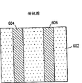
As mentioned above, technology described herein can be used for producing the IMD decorating film that comprises pattern metal or other patterned film layer in a specific embodiment.The floor map of Fig. 2 A to Fig. 2 D explanation series of process step, these processing steps are used for utilizing on substrate membrane structure to form the simple designs that comprises four vertical bars.Fig. 2 A shows plasticity substrate 202.In Fig. 2 B, comprise that the ink logo of lines 204 has been printed on the substrate 202.In the embodiment that is shown in Fig. 2 B, lines 204 define the zone that four vertical thin-film structures will form thereon on substrate 202, describe more fully as following, in the zone of the substrate 202 that is not covered by lines 204.
In Fig. 2 C, thin layer 206 has been formed on the patterned surface of substrate, and covering substrate 202 is not by the part (being represented by the dotted line among Fig. 2 C) of printing ink lines 204 coverings with by the part of printing ink lines 204 coverings.In Fig. 2 D, the part that is deposited on the printing ink lines 204 of ink logo and film 206 is stripped from, exposes (a plurality of) membrane structure 208.Single membrane structure 208 by since a plurality of zones of peeling off the substrate 202 that printing ink lines 204 expose by separated from one another.
Fig. 3 A to 3D looks schematic cross-section by the master that the processing step that is shown in Fig. 2 A to Fig. 2 D is provided and further specifies the embodiment that is shown in Fig. 2 A to Fig. 2 D.Fig. 3 A represents that the master of substrate 202 looks sectional view.Fig. 3 B represents to be formed on the printing ink lines 204 on the substrate 202.Shown in Fig. 3 C, thin layer 206 is formed on the part that is not covered by lines 204 of substrate and in the top and the side surface of polymeric oil line of ink marker bar 204.At last, Fig. 3 D is illustrated in and peels off the membrane structure 208 that lines 204 still are formed on the substrate 202 afterwards, and it has following effect: peel off printing ink lines 204 and any thin-film material 206 that is formed on printing ink lines 204 tops.
Though Fig. 2 A-2D and Fig. 3 A-3D explanation form the embodiment of four vertical thin-film structures on the plasticity substrate, can be with any printing coatings/printing ink of pattern arbitrarily so that on substrate, limit the membrane structure of any required form or size.The floor map of an embodiment of Fig. 4 A and Fig. 4 B explanation, a plurality of segmentations that wherein form numeral " 8 " are to utilize a specific embodiment of methods described herein and form.Fig. 4 A represents IMD decorating film 400, and it comprises and cover ink logo 402, and this pattern defines seven film sectional area 404a-404g on the plasticity substrate, and ink logo 402 does not exist in these zones, so that exposes following substrate.Fig. 4 B is illustrated in deposit film and peels off ink logo step same film 400 afterwards.Shown in Fig. 4 B, printing ink peel off the background area 406 that has exposed substrate, do not have membrane structure thereon.In addition, film segmentation 408a-408g has formed and has stayed sectional area 404a-404g, and it is as defined in above-mentioned Fig. 4 A.
As can obviously seeing from above-mentioned, the membrane structure of Any shape or size can be by being limited and formed simply by the area of the pattern that uses printing on the substrate that will form thereon at membrane structure.
In a specific embodiment of the illustrated method of Fig. 1-4, be used for making the coating/printing ink of substrate composing images to comprise Sun Chemical Aquabond AP blue ink and/or Sunester red ink (Sun Chemical company, Northlake, IL), and substrate comprises Melinex 453 polyester (the DuPont Teijin company of 5 mil thick, Hopewell, VA).Printing ink can and utilize the manual doctor kiss coater with 360# anilox roller to apply by stencil.Printing ink available air heating gun carries out drying.By being loaded into, patterned substrate come depositing metal films in the DC magnetron sputtering system to deposit the ITO film up to about 100nm thickness.Patterned substrate can be handled with plasma before depositing metal films.Ink logo and metallic film formed thereon are by at room temperature using acetone (Histological grade (pathological grading), Fisher Scientific company) sprinkling to form the patterned substrate 1 to 2 minute of metallic film thereon and being stripped from.The metallic film that above-mentioned processing step causes forming in ink logo (that is, ITO) is removed with printing ink, stays the zone that does not have the ITO coating on substrate, do not have measurable electrical conductivity in the zone that these ITO have been removed like this.
In a specific embodiment of the illustrated method of Fig. 1-4, utilize manual doctor kiss coater to apply warm red ink (the Environmental Inks and Coatings company of film III, LosAngeles, California) so that comprising 5 mil thick Melinex ST505 polyester (DuPont Teiiin companies, Hopewell, Virginia) limiting pattern or mask on the substrate.By being loaded into, patterned substrate come depositing metal films in the DC magnetron sputtering system to deposit the ITO film up to about 100nm thickness.By spraying 30-60 second, from the patterned substrate washing printing ink of ITO coating with acetone (Histological grade, Fisher Scientific).The ITO that forms on printing ink is removed with printing ink, stays the zone that does not have the ITO coating, is printed with ink logo herein.
In a specific embodiment of the illustrated method of Fig. 1-4, covering ink logo is to utilize GP-217Process Magenta printing ink (Ink Systems company on offset press, Commerce, California) be printed in 4507 polyester (Transilwrap of 5 mil thick, Franklin Park, the Illinois) on.The polyester of inking is loaded in in the vacuum system of aluminum evaporation, at the film thickness of 120nm.The polyester of aluminium coating be immersed in heat (about 80 ℃ of T=) butanone (the calibrating level, Fisher Scientific, MEK) in 15 seconds, gently clean with the cotton that is immersed among the MEK then.This process is from the zone that polyester is peeled off inking, and at the aluminium at printing ink top.This peels off the negative-appearing image of formation from printing ink,, do not have aluminized coating in the zone that is printed with ink logo, and remaining area (that is the non-existent zone of ink logo) then is coated with aluminium that is.
In a specific embodiment of the illustrated method of Fig. 1-4, covering ink logo is to utilize film III to warm up red ink (Environmental Inks and Coatings on Mark Andy 4200 offset presses, Los Angeles, California) prepare in 5 mil thick, 12 " on the roller of wide Melinex 453 polyester (Plastics Suppliers; Fullerton, California).This patterning polyester is loaded in the DC magnetron sputtering system with the about 100nm of deposition ITO film.Before deposition, the sheet material of printing ink coating can be handled with plasma.The polyester of ITO coating is immersed in the container of heat (about 80 ℃ of T=) butanone and utilizes Fisher Scientific FS220H ultrasonic cleaning machine ultrasonic wave to clean 2 minutes then.As the result of ultrasonic cleaning step, printing ink and the ITO that forms at the printing ink top are peeled off from polyester.
Behind depositing metal films, utilize simply to the film that forms in the non-existent zone of coating/ink logo do not have destructive stripping means (as but be not limited to above-mentioned solvent and physics stripping means) ability of peeling off masking coating/printing ink lines helps continuous preparation technology, as roll-to-roll preparation technology, because do not need time-consuming intermittently operated, as graph exposure and development photoresist, etch away not the part thin layer that is covered by photoresist or utilize and need the solvent of specially treated or condition after etching, to remove the photoresist layer.By saving time and using more cheap material, method described herein is more much lower than the method cost that other is commonly used to the various types of structures described herein of formation on polymer matrix film.The existence of redispersible particle has improved the resistance to blocking of coated film significantly and and then has widened the process window of roll-to-roll technology in masking coating/printing ink.In addition, the redispersible particle improves the rippability that is deposited on the film on masking coating/printing ink widely.
Fig. 5 A-1 to Fig. 5 D-2 explanation is used replaceable method in the specific embodiment of a formation patterned film design on substrate.The replaceable method that is shown in Fig. 5 A-1 to Fig. 5 D-2 is used the image of " just " printing on following meaning: coating/printing ink is that the pattern with the membrane structure that will form prints, rather than is used to limit the zone that membrane structure will can not form as relevant with Fig. 1-4 as described in top.The illustrated method of Fig. 5 A-1 to Fig. 5 D-2 is similar to the method shown in Fig. 1-4 aspect following: the method that is shown in Fig. 5 A-1 to Fig. 5 D-2 uses printing technology to limit the membrane structure that will form.Yet the method that is shown in Fig. 5 A-1 to Fig. 5 D-2 is different from the method shown in Fig. 1-4 aspect following: the pattern of printing is not peeled off from substrate, describes more fully as following.
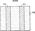
Shown in Fig. 5 A-1 and Fig. 5 A-2, membrane structure is formed on the substrate 502.Substrate 502 can be any above-mentioned substrate material that supplies the usefulness of method shown in Fig. 1-4.In a specific embodiment, substrate comprises 4507 polyester (can be available from Transilwrap, Franklin Park, Illinois) of 5 mil thick.Fig. 5 B-1 and Fig. 5 B-2 show the pattern line 504 and 506 that is printed on the substrate 502.In a specific embodiment, pattern line 504 and 506 is to utilize GP20011 UV Process Magenta printing ink (InkSystems company, Commerce, California) to be printed on the substrate 502 on offset press.But can use any printing ink or other printing material with following characteristics: be attached to substrate with it and compare, Chen Ji film more effectively is attached to this materials printed thereafter, as following explanation more fully.
Fig. 5 C-1 and Fig. 5 C-2 show the thin layer 508 of the patterned surface that is formed on substrate, the zone of the pattern (lines 504 and 506) of covering printing and the pattern covers that is not printed of substrate 502.In a specific embodiment, the formation of film 508 is by patterned substrate being loaded into in the vacuum system of aluminum evaporation, at the film thickness of 120nm.
Fig. 5 D-1 and Fig. 5 D-2 are presented at stripping means and have removed remaining structure after the part film that is formed on the substrate 502 508. Membrane structure 510 and 512 still is respectively formed on the lines 504 and 506 of printing.In a specific embodiment, solvent is used to remove and is formed directly into on-chip part film, but does not remove the part film that is formed on the materials printed, stays the membrane structure with the materials printed identical patterns.In a specific embodiment that is not shown in Fig. 5 D-1 and Fig. 5 D-2, some or all films that are formed on the side of printing material still are attached to the side of printing material behind stripping process.In a specific embodiment, not allly be formed directly into on-chip film and remove, but be formed directly into that on-chip film is sufficiently removed so that see seldom or can't see thin-film material in the substrate region that does not have printing material by stripping process.
The replaceable method that is shown in Fig. 5 A-1 to Fig. 5 D-2 requires: thin layer is lower to the adhesive force of substrate, thin layer is higher to the adhesive force of printing material, printing material is higher to the adhesive force of substrate, and solvent is such, it is removed and is formed directly into on-chip part thin layer, but does not remove the part thin layer that is formed on the printing material.
Replaceable but in the preferable methods, can use semi-finished product IMD film at another, it comprises substrate, separation layer and the durable layer that has bad affinity with film.In such specific embodiment, can use surface treatment, tack coat or priming coat such as ultraviolet curable polymer layer, it all has good adhesive force to durable layer and film.In this case, can in stripping process, be removed to be emerging in the design drawing at surface treatment or priming coat top at the film on the uncoated area.This interchangeable method is similar to the method that is shown in Fig. 5 A-1 to Fig. 5 D-2, has tack coat or priming coat (not shown), and it comprises printing material, as pattern line 504 and 506.If durable layer demonstrates the high affinity to film, then can before tack coat and printing material, masking coating/printing ink be coated durable layer equably.There is not the film on the zone of printing material can in stripping process, be removed to be emerging in the design drawing at printing material and tack coat top.
Fig. 6 A-1 to Fig. 6 F-2 explanation is shown in the other replaceable method of the method for Fig. 1-4.Fig. 6 A-1 and Fig. 6 A-2 display substrate 602.In Fig. 6 B-1 and Fig. 6 B-2, pattern line 604 and 606 has used printable first kind of material to be printed in substrate 602.In a specific embodiment, shown in Fig. 6 C-1 and Fig. 6 C-2, be coated with second kind of material through the substrate of printing is outer then, but it is to be insoluble in the soluble solvent at least a first kind of printing material, but consequently described at least a solvent can be used to peel off first kind of printing material and can not peel off second kind of material.In a specific embodiment, printable first kind of material is that hydrophobic (that is, refusing water) and solvent are soluble and have a low surface tension.In a specific embodiment, second kind of material be water-based and repelled by first kind of material so that external coating only is attached to the part substrate that those are not covered by first kind of material, forms the zone 608,610 and 612 that comprises second kind of (water-based) material.In an interchangeable specific embodiment, second kind of material do not repelled by first kind of material and second kind of material can partially or completely extraterrestrial coating Fig. 6 C-1 and Fig. 6 C-2 shown in pattern line 604 and 606.In such specific embodiment, the zone of first kind of material of coating outside second kind of material, the thickness of second kind of material may be littler than the zone (that is, not printing the on-chip zone of first kind of material) that directly puts on substrate at second kind of material.In a specific embodiment, peeling off of first kind of material is to utilize the suitable solvent of not peeling off second kind of material, stay the structure shown in Fig. 6 D-1 and Fig. 6 D-2, structure 604 and 606 comprising first kind of material has been stripped from, stays the structure 608,610 and 612 that comprises second kind of material on substrate 602.In a specific embodiment, wherein second kind of material can be coated on, at least in part, first kind of material of printing, so being formed on second kind of material of first kind of part on the material is stripped from first kind of material of part that they form thereon, stay the second kind of material of part (that is) that directly puts on substrate, shown in Fig. 6 D-1 and Fig. 6 D-2 in first kind of non-existent zone of material.In a specific embodiment, but be used for peeling off first kind of printing material (and, if suitable, second kind of material of the part of Xing Chenging thereon) solvent comprise the aqueous solution or water.In a specific embodiment, but the solvent that is used for peeling off first kind of printing material comprises non-aqueous solvent or solution.Then, shown in Fig. 6 E-1 and Fig. 6 E-2, use one of above-mentioned thin-film material, film 614 is formed on structure 608,610 and 612 and on the part that is not covered by second kind of material of substrate 602.In a specific embodiment, the formation of film is by spraying plating, vapour deposition, spraying or other suitable technology.At last, Fig. 6 F-1 and Fig. 6 F-2 are presented at appropriate solvent or suitable chemistry or the mechanical stripping method of another kind and peel off the membrane structure 616 and 618 that stays after second kind of material.In a specific embodiment, the solvent that is used for peeling off first kind of material is an alkaline aqueous solution, and the solvent that is used for peeling off second kind of material is acidic aqueous solution, neutral aqueous solution or water.In a specific embodiment, the solvent that is used for peeling off first kind of material is an acidic aqueous solution, and the solvent that is used for peeling off second kind of material is alkaline aqueous solution, neutral aqueous solution or water.In a specific embodiment, the solvent that is used for peeling off first kind of material is neutral aqueous solution or water, and the solvent that is used for peeling off second kind of material is acidic aqueous solution or alkaline aqueous solution.
Among method shown in Fig. 6 A-1 to Fig. 6 F-2, the printed patterns of first kind of material comprises the erect image of the membrane structure that will form.After first kind of material was stripped from, as above-mentioned, second kind of remaining material comprised the negative-appearing image of the membrane structure that will form.In some sense, first kind of material can be counted as mask, and it can be used for limiting has very undersized zone, and as very thin lines, wherein membrane structure will not exist.Though it is initial with practical printing technology, as offset printing technology, it may be difficult printing narrow lines like this, for example because physical restriction, the diffusion or the like of printing ink after printing, not very thin lines or be not very little zone but such technology can be used for easily printing only have separation lines or a zone closely spaced.So can be used to fill the narrow gap between the zone that covers by first kind of material as second kind of above-mentioned material, utilize the peelable first kind of material of appropriate solvent then, stay the very thin lines or other shape that comprise second kind of material, and print this very thin lines at first or shape may be unpractiaca.Can use these lines then, as mentioned above, as, for example, form the negative-appearing image of the adjacent membrane structure of opening by very narrow separated.
In a specific embodiment, the physics stripping means is used to appear the patterned film structure as peeling off.For example, the adhesive tape that ITO is had suitable adhesion strength and a bonding strength is laminated to and preprints the ITO/PET film that is brushed with masking coating/printing ink.Thereafter peel off the ITO that will remove being printed with on the zone on the zone of covering printing ink or that do not having printing ink, it depends on the adhesion strength of printing ink and in the bonding strength at printing ink-PET and ITO-PET interface.This lift-off technology can use together with any above-mentioned method.
In a specific embodiment, the method of Fig. 6 A-1 to Fig. 6 F-2 comprises: on MarkAndy 4200 offset presses, use warm red ink (the Environmental Inksand Coatings of film III, Morganton, the North Carolina), with the erect image of needed conducting membrane structure be printed onto Melinex 582 polyester rollers (4 mil thick, 14 " wide, Dupont TeijinFilms; Wilmington, DL) on.Then the printing of polyester roller utilize the rod coating of 6# Meyer with a solution and 80 ℃ in baking oven dry 1.5 minutes, this solution comprises 16 parts moisture 10% polyvinylpyrrolidone (PVP-90, ISP Technologies company, Wayne, the New Jersey), 0.40 part of Sunsperse Violet (Sun Chemical, Cincinnati, the Ohio) and 16 parts of water.Then this film is placed in the crystallising dish that contains ethyl acetate.With 10 " * 10 " * 12.5 " ultrasonication bathe (by 12TMultiSonik
TMThe BLACKSTONE-NEY that generator drives, PROT-0512H EP ultra sonic bath) fill about 4 " water, and the ware that will contain this film floats in the water, ultrasonication 5 minutes under 104KHz then.Then from ware remove this film and 80 ℃ baking oven dry 1.5 minutes.When finishing drying steps, this film has the lines of PVP coating, and it limits the negative-appearing image of the erect image of initial printing.Then utilize CHA Mark 50 roll coaters with ITO spraying plating coated pattern polyester to deposit the thick ITO film of 1250 dusts.The patterning polyester ultrasonication that in containing the beaker of water ITO is coated with is 3 minutes then, and wherein beaker is to be placed in the Fisher #FS220H sonicator (Fisher Scientific, Pittsburg, Pennsylvania).Then with this film with deionized water rinsing and blow moisture content off with air-flow and carry out drying.The film that generates has the ITO structure, and it is shaped as the erect image of initial printing.
In a specific embodiment, the method that is shown in Fig. 6 A-1 to Fig. 6 F-2 is included in sputtering deposition ITO film on the PET substrate, and this substrate has hydrophilic coating, and for example, Melinex 582, and utilizes warm red ink (Environmental Ink) to print.In a specific embodiment, the combination of this material makes and can utilize the water-based remover to peel off ITO from unwanted zone ultrasonically.
In a specific embodiment, being used for the water-based remover that ITO peels off can be surfactant solution, as JEM-126 (sodium tripolyphosphate, sodium metasilicate, nonyl phenol ethoxylate, ethylene glycol monobutyl ether (EGMBE) and NaOH), detergent compositions 409, hydroperoxides and developer Shipley 453 or the like.
In a specific embodiment, the ITO detachment rate depends on solvent strength, solvent temperature and the substrate membrane position with respect to ultrasonic transducer.
In a specific embodiment, before the ITO sputtering deposition, the pet sheet face of ink printing carries out preliminary treatment with suitable plasma.In a specific embodiment, such plasma preliminary treatment will be in the ITO stripping process on patterning ITO structure the generation of the micro-crack degree that minimizes.In addition, such plasma preliminary treatment can prevent to produce the ITO residue on the inked areas of printing in a specific embodiment, this is the result owing to the ink logo of removing the part printing with energetic plasma, and it can produce the ITO residue on the inked areas of printing in stripping process.
In order to eliminate the optical effect that appears at the lip-deep less printing ink residue of the ITO that peels off, in a specific embodiment, the colorless ink that is printed on the pet sheet face is preferred.
Be used for can be used on the plasticity substrate, form patterned metal layer, to be provided at the IMD decorating film that comprises such patterned metal layer in its design in any aforementioned techniques that forms the patterned film design on the substrate.These technology are applicable to but are not limited to in-mold transfer printing and mould is embedded in IMD.
Fig. 7 is a flow chart, illustrates to be the employed method of formation in-mold transfer printing type IMD film in a specific embodiment, wherein uses one or more the techniques described herein to come to form the patterned film structure on substrate.This method starts from step 702, and wherein the coating of PET substrate is with separation layer.In a specific embodiment, coating about 0.1-3 μ m, preferred 0 on 2 mil PET substrate layers.The separation layer of 3-2 μ m thickness.In step 704, treated substrate is coated with durable layer to obtain oil resistivity and resistance to scraping.In a specific embodiment, durable layer is about the 2-10 micron, is preferably the thickness of 4-8 μ m.In step 706, formed the patterned film part of IMD design.In a specific embodiment, step 706 comprises one or more technology of describing among top and Fig. 1 to Fig. 6 D, is used for forming on substrate the patterned film structure.In a specific embodiment, step 706 comprises utilizes one of technology described herein to form patterned metal layer on substrate.In step 708, use any suitable printing ink on substrate, to print any extra pattern, to obtain visual effect.Be coated with substrate and layout in step 710 with adhesive then.The IMD decorating film that produces can be used in the inner mould transfer printing technology, is transferred to injection-molded article so that will design thing.
Fig. 8 is a flow chart, illustrates in a specific embodiment to be embedded in the employed method of type IMD film for forming mould, wherein uses one or more the techniques described herein to come to form the patterned film structure on substrate.In step 802, the patterned film of IMD design partly is formed in, for example, and on Merlon (PC) or acrylic acid (PMMA) substrate.In a specific embodiment, step 802 comprises one or more technology of describing among top and Fig. 1 to Fig. 6 D, is used for forming on substrate the patterned film structure.In a specific embodiment, step 802 comprises utilizes one of technology described herein to form patterned metal layer on substrate.In step 804, use any suitable printing ink on substrate, to print any extra pattern.Substrate and layout are coated with in step 806 with thin layer then with protection printing ink.The IMD decorating film that produces can be used on mould and is embedded in the technology so that layout is transferred to injection-molded article.
The additional embodiment of enumerating below (being labeled as specific embodiment A to F) with relatively convenient, image according to film forms and relevant manufacturing and processing method, further specify, for example, the advantage that in masking coating/printing ink, comprises redispersible particle (as described herein), as in the above with Fig. 1 to Fig. 4 B in the method described.
In specific embodiment A, following shielding layer composition is used for aluminium (Al) metallic film image and forms: 5.5 gram Celvol 203S (PVA, from Celanese, Dallas, Texas, low-molecular-weight, 87% hydrolysis), 5.5 gram PVP K-30 (from ISP company, Wayne, New Jersey) and 0.1 gram xanthans are (from Allchem company, Dalton, the Georgia State) at room temperature slowly is dissolved in the deionized waters of 39.2 grams.In shading composition, add 0.23 gram Silwet L-7608 (from OSi Specialties, Middlebury, the Connecticut State).The solution that produces is used for printed patterns on substrate as masking coating/printing ink, is used for metallization, and is for example, as described herein.
In specific embodiment B, following shielding layer composition is used for aluminium (Al) metallic film image and forms: (Sylojet 703C, from GraceDavison, Columbia MD) dilutes with 36.2 gram deionized waters the dispersed silicon dioxide of 3.0 grams 20%.Under the room temperature, in this solution, slowly add 5.2 gram Celvol 203S, 5.2 gram PVP K-30 and 0.1 gram xanthans, under high-rate of shear, mix then.At last, add 0.23 gram SilwetL-7608.The solution that produces is used for printed patterns on substrate as masking coating/printing ink, is used for metallization, and is for example, as described herein.
In specific embodiment C-F, used step and the adhesive identical with specific embodiment B, difference is: the percetage by weight of silica changes to 10%, changes to 30% in specific embodiment D, change to 60% and change to 80% in specific embodiment F in specific embodiment E in specific embodiment C in dry film.
For the purpose of comparison, all in above-mentioned specific embodiment A-F are covered solution and are screen printed by 330 order stencils that (ICI is UK) to form the negative pattern that covers in 2 mil Melinex, 453 PET films.The performance of rolling of print film is to assess with resistance to blocking under environment and 50 ℃/80% RH condition.The PET film of printing is by the aluminium lamination of the even coating of vapour deposition with 50-60nm thickness.By optionally removing the aluminium lamination on shielding layer, positive aluminium pattern develops in water so that produce positive aluminium pattern in the zone that is not printed with shielding layer.Rippability or to peel off selectivity be that definition and gloss by the aluminium image that produces is determined.The results are shown in the following table 1 (be used for specific embodiment at data of each row letter representation) by first row:
Table 1
| Adhesive PVA/PVP K-30 (1:1) | Silica (percetage by weight in dry film) | The serigraphy quality | Film coalescence under environmental condition | Film coalescence after wearing out under 50 ℃/80% RH condition | Water is to the rippability of aluminium | |
| A | 97 | 0% | Well | Adhesion | Serious adhesion | Well |
| B | 92 | 5% | Well | Fabulous | Well | Well |
| C | 87 | 10% | Well | Fabulous | Fabulous | Fabulous |
| D | 67 | 30% | Well | Fabulous | Fabulous | Fabulous |
| E | 37 | 60% | Well | Fabulous | Fabulous | Fabulous |
| F | 17 | 80% | Medium | Fabulous | Fabulous | Fairly good |
As can be seen from Table 1, be benchmark and calculate by weight that the particulate silica that adds 5wt% to 80wt% has been improved the resistance to blocking of shielding layer and the rippability of the aluminium lamination on the shielding layer significantly with dried shielding film.The existence of particle dispersion also causes having the high glaze aluminum steel bar of hachure width and fabulous integrality in shielding layer.
In a specific embodiment, the in-mold decoration film, as above in conjunction with Figure 7, comprise separation layer, it is prepared as follows: 15.0 gram CYMEL 303ULF are (from CytecIndustries company, West Paterson, the New Jersey) under 600 rev/mins condition, mixed 5 minutes with 105 gram MEK.Adding 0.3 gram CYCAT600 (from CytecIndustries company, West Paterson, New Jersey) also stirred under 600 rev/mins condition 5 minutes again.The solution that generates filters with 0.2 micron filter then and coats 1.42 mil PET (SH22 is from SKC company, Korea S) with 4# Meyer rod, and target thickness is 1 μ m.Dry this coated film of air 5 minutes and 130 ℃ of bakings 10 minutes in baking oven then.
In a specific embodiment, the in-mold decoration film, as top described in conjunction with Figure 7, comprise durable layer, it is prepared as follows: (Elvacite 2041 (the PMMA resin is from Lucite International company) of 20% in the weight ratio=9:1) and 320 restrains that (EB1290 (from UCB Chemicals company) of 25% in the weight ratio=9:1) fully mixes at the MEK/ cyclohexanone to 500 grams at the MEK/ cyclohexanone.In this solution, add 67 gram MEK-ST (from Nissan Chemical) mechanical agitation simultaneously.At last, add 24 grams at MEK/ cyclohexanone (photoinitiator (the Irgacure907/Irgacure 1800=1:1 of 25% in the weight ratio=9:1), w/w is from Ciba Specialty Chemicals) and 89 gram MEK/ cyclohexanones (weight ratios=9:1) also stirred again 30 minutes.This solution is coated separation layer coated film and this coating air drying 30 minutes with No. 22 coiling rods, then 65 ℃ of dryings 10 minutes to produce the thick durable layer coating of 6-7 μ m (doing).
In a specific embodiment, the in-mold decoration film, as top described in conjunction with Figure 7, comprise patterned aluminium layer, it is prepared as follows: the shielding layer that prints above-mentioned specific embodiment C as the durable layer of preparation as described in the epimere by serigraphy, by vapour deposition coating with the thick aluminium lamination of about 60nm, thereby then by the water flushing to remove aluminium on the printing shielding layer glossiness, the high-resolution aluminium pattern that develops.
In a specific embodiment, as the top and common description of Fig. 7, the adhesive phase that comprises the in-mold decoration film comprises adhesive phase, it is prepared as follows: 2.5 gram Sancure2710 are (from Noveon company, Cleveland, the Ohio) and 7.5 gram deionized waters fully mix then with 16# Meyer rod coat as tight go up save as described in the patterned aluminium layer of preparation, target thickness is 2-3 μ m.Coated film in 90 ℃ baking oven dry 1 minute then.
In a specific embodiment, be put into injection molding as the multilayer film of preparation as described in four sections of the fronts, then the PMMA resin by injection-molded to adhesive phase.After barrier film was stripped from, durable layer and patterned aluminium layer were transferred to molded item fully.
The above is the preferred embodiments of the present invention only, is not limited to the present invention, and for a person skilled in the art, the present invention can have various changes and variation.Within the spirit and principles in the present invention all, any modification of being done, be equal to replacement, improvement etc., all should be included within protection scope of the present invention.
Claims (56)
1. method that forms membrane structure on substrate may further comprise the steps:
Utilize peelable material printed patterns on described substrate of mainly forming by adhesive and the redispersible particle of calculating by weight 5-80%, the peelable material of described printing is at the negative-appearing image that is limited to the decoration design that will form on the described substrate on the described substrate, so that the peelable material of described printing is present in the zone that described on-chip described membrane structure can not form and the peelable material of described printing is not present in the zone that described on-chip described membrane structure will form basically;
Deposit film material on described substrate; And
Peel off described peelable material from described substrate;
Described thus peelable material and any thin-film material that forms thereon are removed by described peeling off, and stay the described membrane structure that the shape with described decoration design forms on described substrate;
Wherein said substrate and the described membrane structure that forms thereon are suitable for as the IMD decorating film.
2. the method that forms membrane structure on substrate according to claim 1, wherein said peelable material are mainly formed by adhesive and the described redispersible particle of calculating by weight 10-60%.
3. the method that forms membrane structure on substrate according to claim 1, wherein said adhesive is water-soluble or aqueous dispersion polymers.
4. the method that on substrate, forms membrane structure according to claim 3, wherein said water-soluble or aqueous dispersion polymers is to be selected from by polyvinyl alcohol, polyvinylpyrrolidone, polyvinyl pyridine, polyacrylic acid, polymethylacrylic acid, polyacrylamide, polyethylene glycol, ethene-maleic anhydride copolymers, vinyl ethers-maleic anhydride copolymers, styrene-maleic anhydride copolymers, butylene-itaconic acid copolymer, PEO, the polystyrolsulfon acid ester, cellulose derivative, xanthans, gum arabic, gelatin, lecithin, with and the group formed of copolymer.
5. the method that on substrate, forms membrane structure according to claim 3, wherein said water-soluble or aqueous dispersion polymers is an aqueous dispersion polymers, is selected from the group of being made up of water dispersible or the dispersed wax of alkali, polyolefin and acrylic based emulsion or dispersion.
6. the method that forms membrane structure on substrate according to claim 1, wherein said adhesive is dissolution with solvents or solvent polymer dispersion.
7. the method that forms membrane structure on substrate according to claim 1, wherein said redispersible particle is derived from silica, CaCO
3, CaSO
4, BaSO
4, Al
2O
3, TiO
2, hollow spheres, non-film forming latex or dispersion, inorganic pigment or organic pigment.
8. the method that forms membrane structure on substrate according to claim 1, wherein said redispersible particle is polymer particles or polymer composite particles.
9. the method that on substrate, forms membrane structure according to claim 1, wherein said peelable material also comprises an additive, is selected from the group of being made up of surfactant, dyestuff, curing agent and plasticizer; Thereby the existence of described additive promotes to peel off described peelable material after the deposition of described thin-film material.
10. the method that forms membrane structure on substrate according to claim 1, wherein said strip step comprise uses solvent to remove described peelable material.
11. the method that on substrate, forms membrane structure according to claim 10, wherein said solvent be select Free water, the aqueous solution, alcohol, ketone, ester, ether, acid amides, hydrocarbon, alkylbenzene, pyrrolidones, sulfone, dimethyl sulfoxide (DMSO), with and composition thereof the group formed with derivative.
12. the method that forms membrane structure on substrate according to claim 1, wherein said thin-film material is non-conductive.
13. the method that forms membrane structure on substrate according to claim 1, wherein said thin-film material is semi-conductive.
14. the method that forms membrane structure on substrate according to claim 1, wherein said thin-film material conducts electricity.
15. the method that on substrate, forms membrane structure according to claim 14, wherein said conductive film material be selected from by metal, metal oxide, with and the material of the group formed of alloy and multilayer materials.
16. the method that on substrate, forms membrane structure according to claim 14, wherein said conductive film material is a metal, is selected from the group of being made up of aluminium, copper, zinc, tin, molybdenum, nickel, chromium, silver, gold, iron, indium, thallium, titanium, tantalum, tungsten, rhodium, palladium, platinum and cobalt.
17. the method that on substrate, forms membrane structure according to claim 14, wherein said conductive film material is metal oxide or sulfide, is selected from by the indium oxide of tin indium oxide, indium zinc oxide, aluminum zinc oxide, gadolinium oxide indium, tin oxide, doped with fluorine and the group that zinc sulphide is formed.
18. the method that forms membrane structure on substrate according to claim 1, the step of wherein said deposit film material comprises spraying plating.
19. the method that forms membrane structure on substrate according to claim 1, the step of wherein said deposit film material comprises vapour deposition.
20. the method that forms membrane structure on substrate according to claim 1, the step of wherein said deposit film material comprises vacuum deposition.
21. the method that forms membrane structure on substrate according to claim 1, the step of wherein said deposit film material comprises plating.
22. the method that forms membrane structure on substrate according to claim 1, the step of wherein said deposit film material comprises electroless plating.
23. the method that forms membrane structure on substrate according to claim 1, the step of wherein said deposit film material comprises electroforming.
24. the method that forms membrane structure on substrate according to claim 1, wherein said print steps comprises hectographic printing.
25. the method that forms membrane structure on substrate according to claim 1, wherein said print steps comprises driography.
26. the method that forms membrane structure on substrate according to claim 1, wherein said print steps comprises electrophotographic printing.
27. the method that forms membrane structure on substrate according to claim 1, wherein said print steps comprises litho.
28. the method that forms membrane structure on substrate according to claim 1, wherein said print steps comprises photogravure.
29. the method that forms membrane structure on substrate according to claim 1, wherein said print steps comprises the temperature-sensitive printing.
30. the method that forms membrane structure on substrate according to claim 1, wherein said print steps comprises ink jet printing.
31. the method that forms membrane structure on substrate according to claim 1, wherein said print steps comprises serigraphy.
32. the method that forms membrane structure on substrate according to claim 1, wherein said print steps comprises letterpress.
33. the method that forms membrane structure on substrate according to claim 1, wherein said substrate comprises the plasticity substrate.
34. the method that forms membrane structure on substrate according to claim 33, wherein said plasticity substrate comprises part plasticity substrate roller.
35. the method that forms membrane structure on substrate according to claim 34, the wherein said method that forms membrane structure on substrate are the parts of the roll-to-roll technology of preparation IMD decorating film.
36. the method that forms membrane structure on substrate according to claim 1, wherein said substrate comprises the PETG film.
37. the method that forms membrane structure on substrate according to claim 36 further is included in and carries out following step on the described substrate before the described membrane structure of formation:
Handle or be coated with described PET film with releasing agent or coating; And
With durable layer be coated with described treated or through the coating the PET film so that oil resistivity and resistance to scraping to be provided.
38. the method that forms membrane structure on substrate according to claim 36 uses second of the printing material printing that is different from described thin-film material to decorate design but further be included on the described substrate.
39. the method that forms membrane structure on substrate according to claim 36 further comprises with adhesive being coated with described IMD decorating film to form the in-mold transfer printing film.
40. the method that forms membrane structure on substrate according to claim 1, wherein said substrate comprises polycarbonate substrate.
41., further comprise with thin protective layer being coated with described IMD decorating film according to the described method that on substrate, forms membrane structure of claim 40.
42. comprising, the method that forms membrane structure on substrate according to claim 1, wherein said strip step use mechanical pressure to remove described peelable material.
43., wherein use mechanical pressure to comprise brushing according to the described method that on substrate, forms membrane structure of claim 42.
44., wherein use mechanical pressure to comprise and utilize nozzle according to the described method that on substrate, forms membrane structure of claim 42.
45. the method that forms membrane structure on substrate according to claim 1, wherein said strip step comprises:
Apply adhesive phase, with respect to the bonding strength of described peelable material to described substrate, described adhesive phase has higher bonding strength to described thin-film material and/or peelable material; Bonding strength between the adhesion strength of described thin-film material and thin-film material and the described substrate is better than the bonding strength of adhesive phase to described thin-film material and/or peelable material; Bonding strength between described thin-film material and the described peelable material is better than the bonding strength between peelable material and the described substrate; And
Remove described peelable material and formation any thin-film material thereon by peeling off described adhesive phase.
46. the method that forms membrane structure on substrate according to claim 1, wherein said strip step comprises:
Behind described deposition step, adhesive phase is put on described substrate; And remove described thin-film material in zone with described peelable material by peeling off described adhesive phase, wherein with respect to the bonding strength of described peelable material to described substrate, described adhesive phase has higher bonding strength to described thin-film material and/or peelable material; Bonding strength between the adhesion strength of described thin-film material and thin-film material and the described substrate is better than the bonding strength of adhesive phase to described thin-film material and/or peelable material; Bonding strength between described thin-film material and the described peelable material is better than the bonding strength between peelable material and the described substrate.
47. a method that forms membrane structure on substrate may further comprise the steps:
With first kind of material printed patterns on described substrate, described pattern is limited to the erect image of the decoration design that will form on the described substrate, so that described first kind of material is printed on the zone that described membrane structure will form, and described first kind of material can use first kind of solvent to peel off;
With the surface through printing of the described substrate of the outer coating of second kind of material, wherein said second kind of material is not peelable with described first kind of solvent;
In a process, utilize described first kind of solvent to peel off described first kind of material, wherein said process is peeled off described first kind of material and is formed on the described second kind of material on described first kind of material and does not peel off and be formed directly into second kind of material on the described substrate, so that described second kind of material still is coated on described first kind of material and do not exist on the described substrate, limits the negative-appearing image of the decoration design that will form so that described second kind of material whereby and still be present in and do not form described membrane structure zone on described substrate;
Deposit film material on described substrate; And
Peel off removing described second kind of material and to be deposited on thin-film material on described second kind of material, thereby form described membrane structure with the shape of described decoration design;
Wherein said substrate and the described membrane structure that forms thereon are suitable for as the IMD decorating film.
48. according to the described method that on substrate, forms membrane structure of claim 47, wherein said first kind of material repels described second kind of material, so that described second kind of material filled the zone of the described substrate that does not print described first kind of material and be not coated with the zone that described first kind of material exists.
49. according to the described method that forms membrane structure on substrate of claim 47, wherein said first kind of solvent is the aqueous solution or water.
50. according to the described method that forms membrane structure on substrate of claim 47, wherein said first kind of solvent is nonaqueous solvents or solution.
51. according to the described method that on substrate, forms membrane structure of claim 47, wherein said first kind of solvent is alkaline aqueous solution, and the described step of peeling off described second kind of material comprises and uses second kind of solvent, comprises acidic aqueous solution, neutral aqueous solution or water.
52. according to the described method that on substrate, forms membrane structure of claim 47, wherein said first kind of solvent is acidic aqueous solution, and the described step of peeling off described second kind of material comprises and uses second kind of solvent, comprises alkaline aqueous solution, neutral aqueous solution or water.
53. according to the described method that on substrate, forms membrane structure of claim 47, wherein said first kind of solvent is neutral aqueous solution or water, and the described step of peeling off described second kind of material comprises and uses second kind of solvent, comprises acidic aqueous solution or alkaline aqueous solution.
54. a method that forms membrane structure on substrate may further comprise the steps:
Utilize mainly and print first pattern by adhesive and the peelable material that the redispersible particle of calculating by weight 10-60% is formed on first surface of described substrate, first pattern of described peelable material limits the negative-appearing image of first membrane structure that will form on described first surface of described substrate;
Deposit film material on described first surface of described substrate;
Peel off described first pattern of peelable material from described substrate;
Utilize mainly and print second pattern by adhesive and the peelable material that the redispersible particle of calculating by weight 10-60% is formed on second surface of described substrate, second pattern of described peelable material limits the negative-appearing image of second membrane structure that will form on described second surface of described substrate;
Deposit film material on described second surface of described substrate; And
Peel off described second pattern of described peelable material from described substrate;
Remove described second pattern of described first pattern of described peelable material, described peelable material thus and be formed on any thin-film material on described first or described second pattern of described peelable material, stay described first membrane structure on described first surface of described substrate and described second membrane structure described second surface at described substrate;
Wherein said first membrane structure comprises first decoration design, and described second membrane structure comprises that second is decorated design, and the described membrane structure of described substrate and formation thereon is suitable for being used as the IMD decorating film.
55. a method that forms membrane structure on substrate may further comprise the steps:
Utilize mainly and print first pattern by adhesive and the peelable material that the redispersible particle of calculating by weight 10-60% is formed on first surface of described substrate, first pattern of described peelable material limits the negative-appearing image of first membrane structure that will form on described first surface of described substrate;
Utilize mainly and print second pattern by adhesive and the peelable material that the redispersible particle of calculating by weight 10-60% is formed on second surface of described substrate, second pattern of described peelable material limits the negative-appearing image of second conducting membrane structure that will form on described second surface of described substrate;
Described substrate described first the surface and described second surface on the deposit film material; And
Peel off described first pattern and second pattern of described peelable material from described substrate;
Remove described second pattern of described first pattern of described peelable material, described peelable material thus and be formed on any thin-film material on described first or described second pattern of described peelable material, stay described first membrane structure on described first surface of described substrate and described second membrane structure described second surface at described substrate; And
Wherein said first membrane structure comprises first decoration design, and described second membrane structure comprises that second is decorated design, and the described membrane structure of described substrate and formation thereon is suitable for being used as the IMD decorating film.
56. according to the described method that forms membrane structure on substrate of claim 55, wherein said strip step comprises uses solvent to remove described peelable material.
Applications Claiming Priority (2)
| Application Number | Priority Date | Filing Date | Title |
|---|---|---|---|
| US10/665,992 US7156945B2 (en) | 2002-04-24 | 2003-09-19 | Process for forming a patterned thin film structure for in-mold decoration |
| US10/665,992 | 2003-09-19 |
Publications (2)
| Publication Number | Publication Date |
|---|---|
| CN1597333A CN1597333A (en) | 2005-03-23 |
| CN100537232C true CN100537232C (en) | 2009-09-09 |
Family
ID=34375845
Family Applications (1)
| Application Number | Title | Priority Date | Filing Date |
|---|---|---|---|
| CN200410048743.2A Expired - Fee Related CN100537232C (en) | 2003-09-19 | 2004-06-15 | Process for forming a patterned thin film structure for in-mold decoration |
Country Status (6)
| Country | Link |
|---|---|
| US (1) | US7156945B2 (en) |
| EP (1) | EP1697102A4 (en) |
| JP (1) | JP2007533483A (en) |
| CN (1) | CN100537232C (en) |
| TW (1) | TWI273965B (en) |
| WO (1) | WO2005028176A2 (en) |
Families Citing this family (77)
| Publication number | Priority date | Publication date | Assignee | Title |
|---|---|---|---|---|
| TWI268813B (en) * | 2002-04-24 | 2006-12-21 | Sipix Imaging Inc | Process for forming a patterned thin film conductive structure on a substrate |
| US20050102897A1 (en) * | 2003-02-10 | 2005-05-19 | Productivity California, Inc. | Plant container and method for making a plant container |
| US20050107231A1 (en) * | 2003-02-10 | 2005-05-19 | Productivity California, Inc. | Method for printing images and text on a plant container |
| WO2005089480A2 (en) | 2004-03-19 | 2005-09-29 | Stuart Arthur Bateman | Activation method |
| US20060019088A1 (en) | 2004-07-20 | 2006-01-26 | Xiaojia Wang | Adhesive layer composition for in-mold decoration |
| US20060030149A1 (en) * | 2004-08-06 | 2006-02-09 | Steven Leith | Depositing material on photosensitive material |
| US20060076702A1 (en) * | 2004-10-07 | 2006-04-13 | Fu-Chi Tsai | Method of manufacturing a casing of an electronic product with surface decoration thereon |
| ATE460466T1 (en) * | 2005-01-21 | 2010-03-15 | Commw Scient Ind Res Org | ACTIVATION METHOD USING A MODIFICATION AGENT |
| US20070026205A1 (en) | 2005-08-01 | 2007-02-01 | Vapor Technologies Inc. | Article having patterned decorative coating |
| US7767126B2 (en) * | 2005-08-22 | 2010-08-03 | Sipix Imaging, Inc. | Embossing assembly and methods of preparation |
| US20070069418A1 (en) * | 2005-09-28 | 2007-03-29 | Chih-Yuan Liao | In mold manufacturing of an object comprising a functional element |
| US20070241966A1 (en) * | 2006-04-14 | 2007-10-18 | Yung-Shun Chen | Conductive antenna structure and method for making the same |
| SG175689A1 (en) * | 2006-10-27 | 2011-11-28 | Takeoka Shinji | Thin film-like polymer structure and method for preparing the same |
| JP2008165849A (en) * | 2006-12-27 | 2008-07-17 | Fujitsu Ltd | Nano-structure forming method and magnetic disk manufacturing method |
| CN101210338B (en) * | 2006-12-29 | 2010-11-17 | 深圳富泰宏精密工业有限公司 | Multi-color electrophoresis painting method |
| JP4096023B1 (en) | 2007-05-31 | 2008-06-04 | 日本写真印刷株式会社 | Production method of radio wave transmission material |
| GB0716266D0 (en) * | 2007-08-21 | 2007-09-26 | Eastman Kodak Co | Method of patterning vapour deposition by printing |
| GB0718840D0 (en) * | 2007-09-26 | 2007-11-07 | Eastman Kodak Co | Method of patterning vapour deposition by printing |
| WO2009070428A1 (en) * | 2007-11-26 | 2009-06-04 | S.D. Warren Company | Tip printing and scrape coating systems and methods for manufacturing electronic devices |
| US20090149589A1 (en) * | 2007-12-05 | 2009-06-11 | College Of William And Mary | Method for generating surface-silvered polymer structures |
| WO2009103274A1 (en) * | 2008-02-18 | 2009-08-27 | Hologram Industries Research Gmbh | Method for the individual application of hot embossing film and security documents produced therewith |
| TWI353808B (en) * | 2008-04-28 | 2011-12-01 | Ind Tech Res Inst | Method for fabricating conductive pattern on flexi |
| CN101659173B (en) * | 2008-08-28 | 2013-06-19 | 比亚迪股份有限公司 | Method for manufacturing metal patterns |
| EP2177644A1 (en) | 2008-10-14 | 2010-04-21 | Applied Materials, Inc. | Coating of masked substrates |
| CN101722779B (en) * | 2008-10-17 | 2013-04-10 | 华硕电脑股份有限公司 | Membranous layer and method for making same |
| CN101730413A (en) * | 2008-10-27 | 2010-06-09 | 深圳富泰宏精密工业有限公司 | Housing and method for making same |
| US8388885B2 (en) * | 2008-11-18 | 2013-03-05 | General Electric Company | Membrane structure for vacuum assisted molding fiber reinforced article |
| US20100260940A1 (en) * | 2009-04-08 | 2010-10-14 | Mccown James Charles | System and method for depositing metallic coatings on substrates using removable masking materials |
| US8551386B2 (en) * | 2009-08-03 | 2013-10-08 | S.D. Warren Company | Imparting texture to cured powder coatings |
| CN101797789B (en) * | 2009-09-22 | 2015-03-18 | 欧阳雷 | Shape self-adaptive in-mold decorating method |
| EP2319630A1 (en) * | 2009-11-05 | 2011-05-11 | Heidelberger Druckmaschinen AG | Method for multi-colour permanent varnishing of a product |
| TW201207134A (en) * | 2010-08-03 | 2012-02-16 | Hon Hai Prec Ind Co Ltd | Sputtering method |
| CN102345090A (en) * | 2010-08-04 | 2012-02-08 | 鸿富锦精密工业(深圳)有限公司 | Method for coating film |
| CN102373406A (en) * | 2010-08-13 | 2012-03-14 | 鸿富锦精密工业(深圳)有限公司 | Film plating method |
| FR2968241B1 (en) * | 2010-12-02 | 2012-12-21 | Corso Magenta | METHOD FOR MANUFACTURING AN ARTICLE ENABLING THE APPLICATION OF A FILM |
| GB201103258D0 (en) | 2011-02-25 | 2011-04-13 | Ge Healthcare Uk Ltd | Solid support and method of enhancing the recovery of biological material therefrom |
| ITVI20110122A1 (en) * | 2011-05-13 | 2012-11-14 | St Microelectronics Srl | METHOD AND APPARATUS FOR THE MANUFACTURE OF LEAD FRAMES |
| TWI617628B (en) * | 2011-09-02 | 2018-03-11 | 3M新設資產公司 | Protective composition |
| KR20130076354A (en) * | 2011-12-28 | 2013-07-08 | (주)엘지하우시스 | High glossy sheet with metallic effect comprising ultraviolet curable resin |
| CN102642421A (en) * | 2012-04-27 | 2012-08-22 | 广东宏达印业有限公司 | Preparation method and transfer printing method of film capable of being printed in transfer mode |
| US9518317B2 (en) * | 2012-05-11 | 2016-12-13 | General Electric Company | Method of coating a component, method of forming cooling holes and a water soluble aperture plug |
| US10401668B2 (en) | 2012-05-30 | 2019-09-03 | E Ink California, Llc | Display device with visually-distinguishable watermark area and non-watermark area |
| CN102861993B (en) * | 2012-10-09 | 2015-02-04 | 苏州德诚物联科技有限公司 | Laser production process of radio frequency identification antenna |
| TWI550137B (en) * | 2012-12-28 | 2016-09-21 | 鴻海精密工業股份有限公司 | Masking method for surface treating process |
| CN105308219B (en) * | 2013-04-24 | 2017-07-25 | 汽车专利管理和采用有限责任公司 | The method of coat plastics functional unit |
| CN103278936B (en) * | 2013-05-16 | 2015-09-16 | 周国新 | A kind of high light pad pasting leg of spectacles and manufacturing process thereof |
| JP2015022503A (en) * | 2013-07-18 | 2015-02-02 | 株式会社翔栄 | Method of manufacturing touch panel |
| TWI492136B (en) * | 2013-10-11 | 2015-07-11 | Aevoe Inc | Protective device of portable mobile device |
| FR3013739B1 (en) * | 2013-11-28 | 2016-01-01 | Valeo Vision | METHOD AND DEVICE FOR COATING THE AUTOMOBILE PIECE |
| CN109353136B (en) * | 2014-06-20 | 2020-08-04 | 3M创新有限公司 | Printing of multiple inks to achieve accurate registration during subsequent processing |
| JP2016029224A (en) * | 2014-07-25 | 2016-03-03 | 株式会社ミマキエンジニアリング | Dyeing method, mask forming apparatus, and method for manufacturing colored article |
| JP6167088B2 (en) * | 2014-09-30 | 2017-07-19 | 日本写真印刷株式会社 | Manufacturing method of decorative products that decorate uneven surfaces, manufacturing method of decorative products and drawing products that decorate uneven surfaces |
| GB201509082D0 (en) * | 2015-05-27 | 2015-07-08 | Landa Labs 2012 Ltd | Coating process |
| WO2017044887A1 (en) | 2015-09-09 | 2017-03-16 | Drawbridge Health, Inc. | Systems, methods, and devices for sample collection, stabilization and preservation |
| CN105645350A (en) * | 2016-03-03 | 2016-06-08 | 上海大学 | Device and method for manufacturing micro-nano structures |
| CN106113380B (en) * | 2016-06-28 | 2018-02-13 | 长春华涛汽车塑料饰件有限公司 | A kind of imitative woven design automotive upholstery processing method |
| CN106646938B (en) * | 2016-11-08 | 2019-09-13 | 武汉华星光电技术有限公司 | A kind of Film patterning method |
| US10802373B1 (en) | 2017-06-26 | 2020-10-13 | E Ink Corporation | Reflective microcells for electrophoretic displays and methods of making the same |
| US10921676B2 (en) | 2017-08-30 | 2021-02-16 | E Ink Corporation | Electrophoretic medium |
| US10698265B1 (en) | 2017-10-06 | 2020-06-30 | E Ink California, Llc | Quantum dot film |
| KR101998290B1 (en) * | 2017-11-29 | 2019-07-09 | 순천대학교 산학협력단 | Method for manufacturing semiconducting ink, and methods for manufacturing diode and rectifying circuit using the semiconducting ink |
| CN108118295A (en) * | 2017-12-21 | 2018-06-05 | 上海银之川金银线有限公司 | A kind of discontinuous vacuum metallization film, wire and preparation method thereof |
| CN107955954B (en) * | 2018-01-16 | 2019-11-12 | 北京中钞钞券设计制版有限公司 | A kind of polymeric release agent applied and its preparation, film forming and application method in electroformed nickel production |
| CN108382118A (en) * | 2018-01-23 | 2018-08-10 | 珠海市瑞明科技有限公司 | Platinum leads to the manufacturing method of version stencil paper |
| CN108513456A (en) * | 2018-03-22 | 2018-09-07 | 广东风华高新科技股份有限公司 | Substrate through holes technique |
| CN108834322A (en) * | 2018-03-30 | 2018-11-16 | 广州大正新材料科技有限公司 | A kind of method of printed circuit |
| CN108745816B (en) * | 2018-06-12 | 2021-12-03 | 业成科技(成都)有限公司 | Gluing method |
| US10676809B2 (en) | 2018-06-20 | 2020-06-09 | Lockheed Martin Corporation | Methods and systems for generating patterns on flexible substrates |
| US11397366B2 (en) | 2018-08-10 | 2022-07-26 | E Ink California, Llc | Switchable light-collimating layer including bistable electrophoretic fluid |
| CN112470066A (en) | 2018-08-10 | 2021-03-09 | 伊英克加利福尼亚有限责任公司 | Drive waveform for switchable light collimating layer comprising a bistable electrophoretic fluid |
| WO2020033789A1 (en) | 2018-08-10 | 2020-02-13 | E Ink California, Llc | Switchable light-collimating layer with reflector |
| CN110077135B (en) * | 2019-04-23 | 2020-07-17 | 捷卡(厦门)工业科技有限公司 | Production process of label with window |
| CN111844569B (en) * | 2019-04-29 | 2022-04-01 | 科勒(中国)投资有限公司 | Method for forming pattern, bathroom product and shielding film |
| CN112659709A (en) * | 2019-10-16 | 2021-04-16 | 嘉饰材料科技(浙江)有限公司 | INS film with surface touch feeling and transparent electroplating effect and preparation method thereof |
| CN113025140A (en) * | 2021-03-09 | 2021-06-25 | 长沙蓝思新材料有限公司 | Vacuum electroplating thermosetting dissolving type protective oil and vacuum electroplating process |
| CN113151769B (en) * | 2021-04-01 | 2022-08-05 | 西安交通大学 | Micropore and microcrack composite toughened millimeter-sized thick ceramic coating and preparation method thereof |
| CN114242924B (en) * | 2021-12-13 | 2023-09-26 | 广东省科学院半导体研究所 | Quantum dot light conversion device and preparation method thereof |
Family Cites Families (90)
| Publication number | Priority date | Publication date | Assignee | Title |
|---|---|---|---|---|
| US606654A (en) * | 1898-07-05 | Combination-chair for children | ||
| US518488A (en) * | 1894-04-17 | Compensator | ||
| US3612758A (en) | 1969-10-03 | 1971-10-12 | Xerox Corp | Color display device |
| US3668106A (en) | 1970-04-09 | 1972-06-06 | Matsushita Electric Ind Co Ltd | Electrophoretic display device |
| US3697679A (en) | 1970-07-01 | 1972-10-10 | Ampex | Automatic threading video recorder |
| GB1423952A (en) | 1973-06-26 | 1976-02-04 | Oike & Co | Process for preparing a metallized resin film for condenser element |
| IT1031474B (en) | 1974-02-12 | 1979-04-30 | Plessey Handel Investment Ag | WORKING FLUID FOR ELECTROPHORETIC DEVICES FOR VISUAL IMAGE TAKING |
| DE2519403A1 (en) * | 1974-04-30 | 1975-11-13 | Fuji Photo Film Co Ltd | CARRIER MATERIAL AND ITS USE IN A PHOTOGRAPHICAL RECORDING MATERIAL |
| US4119483A (en) | 1974-07-30 | 1978-10-10 | U.S. Philips Corporation | Method of structuring thin layers |
| US4022927A (en) | 1975-06-30 | 1977-05-10 | International Business Machines Corporation | Methods for forming thick self-supporting masks |
| US4071430A (en) | 1976-12-06 | 1978-01-31 | North American Philips Corporation | Electrophoretic image display having an improved switching time |
| US4217182A (en) | 1978-06-07 | 1980-08-12 | Litton Systems, Inc. | Semi-additive process of manufacturing a printed circuit |
| US4285801A (en) | 1979-09-20 | 1981-08-25 | Xerox Corporation | Electrophoretic display composition |
| US4345000A (en) | 1979-12-15 | 1982-08-17 | Nitto Electric Industrial Co., Ltd. | Transparent electrically conductive film |
| US4368281A (en) * | 1980-09-15 | 1983-01-11 | Amp Incorporated | Printed circuits |
| JPS57177029A (en) | 1981-04-24 | 1982-10-30 | Reiko Co Ltd | Partial metallization of plastic film |
| US4420515A (en) | 1981-08-21 | 1983-12-13 | Sicpa Holding, S.A. | Metallization process for protecting documents of value |
| US4495981A (en) | 1981-11-02 | 1985-01-29 | Olin Corporation | Process and apparatus for synchronized electromagnetic casting of multiple strands |
| JPS5978987A (en) | 1982-10-29 | 1984-05-08 | マルイ工業株式会社 | Formation of pattern on metal coating |
| JPS59171930A (en) | 1983-03-18 | 1984-09-28 | Matsushita Electric Ind Co Ltd | Electrophoresis display element |
| JPS60150508A (en) | 1984-01-18 | 1985-08-08 | 日本写真印刷株式会社 | Method of producing transparent electrode board |
| JPS60173842A (en) | 1984-02-20 | 1985-09-07 | Canon Inc | Forming method of pattern |
| US4655897A (en) | 1984-11-13 | 1987-04-07 | Copytele, Inc. | Electrophoretic display panels and associated methods |
| US4741988A (en) | 1985-05-08 | 1988-05-03 | U.S. Philips Corp. | Patterned polyimide film, a photosensitive polyamide acid derivative and an electrophoretic image-display cell |
| US4714631A (en) * | 1985-08-28 | 1987-12-22 | W. H. Brady Co. | Rapidly removable undercoating for vacuum deposition of patterned layers onto substrates |
| US4680103A (en) | 1986-01-24 | 1987-07-14 | Epid. Inc. | Positive particles in electrophoretic display device composition |
| GB2207289B (en) * | 1987-06-30 | 1990-12-05 | H R Smith | Metal film patterns on substrates |
| JPH0192356A (en) * | 1987-09-30 | 1989-04-11 | Pentel Kk | Ornamental body and its production |
| DE3743780A1 (en) | 1987-12-23 | 1989-07-06 | Bayer Ag | METHOD FOR IMPROVING THE ADHESIVITY OF CURRENTLY DEPOSITED METAL LAYERS ON POLYIMIDE SURFACES |
| US4977013A (en) | 1988-06-03 | 1990-12-11 | Andus Corporation | Tranparent conductive coatings |
| JPH0295893A (en) | 1988-09-30 | 1990-04-06 | Nissha Printing Co Ltd | Metallic luster pattern transfer material |
| JPH02253692A (en) | 1989-03-27 | 1990-10-12 | Matsushita Electric Ind Co Ltd | Pattern formation and manufacture of panel board |
| US5059454A (en) * | 1989-04-26 | 1991-10-22 | Flex Products, Inc. | Method for making patterned thin film |
| JPH0384521A (en) | 1989-08-29 | 1991-04-10 | Mitsumura Genshiyokuban Insatsujiyo:Kk | Pattering method |
| US4995718A (en) | 1989-11-15 | 1991-02-26 | Honeywell Inc. | Full color three-dimensional projection display |
| US5177476A (en) | 1989-11-24 | 1993-01-05 | Copytele, Inc. | Methods of fabricating dual anode, flat panel electrophoretic displays |
| US5495981A (en) | 1994-02-04 | 1996-03-05 | Warther; Richard O. | Transaction card mailer and method of making |
| US5326865A (en) | 1990-06-08 | 1994-07-05 | Hercules Incorporated | Arylazo and poly(arylazo) dyes having at least one core radical selected from naphthyl or anthracyl and having at least one 2,3-dihydro-1,3-dialkyl perimidine substituent |
| CA2114650C (en) | 1991-08-29 | 1999-08-10 | Frank J. Disanto | Electrophoretic display panel with internal mesh background screen |
| DE4209708A1 (en) | 1992-03-25 | 1993-09-30 | Bayer Ag | Process for improving the adhesive strength of electrolessly deposited metal layers |
| US5310778A (en) * | 1992-08-25 | 1994-05-10 | E. I. Du Pont De Nemours And Company | Process for preparing ink jet inks having improved properties |
| US5279511A (en) | 1992-10-21 | 1994-01-18 | Copytele, Inc. | Method of filling an electrophoretic display |
| US5395740A (en) | 1993-01-27 | 1995-03-07 | Motorola, Inc. | Method for fabricating electrode patterns |
| JPH08510790A (en) | 1993-05-21 | 1996-11-12 | コピイテル,インコーポレイテッド | Method for preparing electrophoretic dispersion containing two types of particles having different colors and opposite charges |
| US5380362A (en) | 1993-07-16 | 1995-01-10 | Copytele, Inc. | Suspension for use in electrophoretic image display systems |
| US6111598A (en) | 1993-11-12 | 2000-08-29 | Peveo, Inc. | System and method for producing and displaying spectrally-multiplexed images of three-dimensional imagery for use in flicker-free stereoscopic viewing thereof |
| US5403518A (en) | 1993-12-02 | 1995-04-04 | Copytele, Inc. | Formulations for improved electrophoretic display suspensions and related methods |
| US5699097A (en) | 1994-04-22 | 1997-12-16 | Kabushiki Kaisha Toshiba | Display medium and method for display therewith |
| US5795527A (en) * | 1994-04-29 | 1998-08-18 | Nissha Printing Co., Ltd. | Method of manufacturing decorated article using a transfer material |
| CN1149894A (en) | 1994-05-26 | 1997-05-14 | 考贝泰利公司 | Fluorinated dielectric suspensions for electrophoretic image displays and related methods |
| US6017584A (en) | 1995-07-20 | 2000-01-25 | E Ink Corporation | Multi-color electrophoretic displays and materials for making the same |
| US6120839A (en) | 1995-07-20 | 2000-09-19 | E Ink Corporation | Electro-osmotic displays and materials for making the same |
| US6120588A (en) | 1996-07-19 | 2000-09-19 | E Ink Corporation | Electronically addressable microencapsulated ink and display thereof |
| US6037058A (en) | 1995-10-12 | 2000-03-14 | Rohms And Haas Company | Particles and droplets containing liquid domains and method for forming in an acueous medium |
| US5835174A (en) | 1995-10-12 | 1998-11-10 | Rohm And Haas Company | Droplets and particles containing liquid crystal and films and apparatus containing the same |
| JP3488012B2 (en) | 1996-03-23 | 2004-01-19 | 藤森工業株式会社 | Plastics board |
| US6080606A (en) | 1996-03-26 | 2000-06-27 | The Trustees Of Princeton University | Electrophotographic patterning of thin film circuits |
| US6117300A (en) | 1996-05-01 | 2000-09-12 | Honeywell International Inc. | Method for forming conductive traces and printed circuits made thereby |
| DE19624071A1 (en) | 1996-06-17 | 1997-12-18 | Bayer Ag | Process for the production of sheet-like metal-coated foils |
| JPH1099775A (en) * | 1996-09-30 | 1998-04-21 | Central Glass Co Ltd | Water-soluble masking agent |
| US5930026A (en) | 1996-10-25 | 1999-07-27 | Massachusetts Institute Of Technology | Nonemissive displays and piezoelectric power supplies therefor |
| US5837609A (en) | 1997-01-16 | 1998-11-17 | Ford Motor Company | Fully additive method of applying a circuit pattern to a three-dimensional, nonconductive part |
| US5961804A (en) | 1997-03-18 | 1999-10-05 | Massachusetts Institute Of Technology | Microencapsulated electrophoretic display |
| US6252624B1 (en) | 1997-07-18 | 2001-06-26 | Idemitsu Kosan Co., Ltd. | Three dimensional display |
| US6067185A (en) | 1997-08-28 | 2000-05-23 | E Ink Corporation | Process for creating an encapsulated electrophoretic display |
| US6232950B1 (en) | 1997-08-28 | 2001-05-15 | E Ink Corporation | Rear electrode structures for displays |
| JP3993691B2 (en) * | 1997-09-24 | 2007-10-17 | 関西ペイント株式会社 | Resist pattern forming method |
| US6131512A (en) | 1998-02-03 | 2000-10-17 | Agfa-Gevaert, N.V. | Printing master comprising strain gauges |
| US5914806A (en) | 1998-02-11 | 1999-06-22 | International Business Machines Corporation | Stable electrophoretic particles for displays |
| DE19812880A1 (en) * | 1998-03-24 | 1999-09-30 | Bayer Ag | Shaped part and flexible film with protected conductor track and process for its production |
| AU3767899A (en) | 1998-04-27 | 1999-11-16 | E-Ink Corporation | Shutter mode microencapsulated electrophoretic display |
| JP4053136B2 (en) | 1998-06-17 | 2008-02-27 | 株式会社半導体エネルギー研究所 | Reflective semiconductor display device |
| JP2000010058A (en) | 1998-06-18 | 2000-01-14 | Hamamatsu Photonics Kk | Spatial light modulating device |
| DE19828846C2 (en) | 1998-06-27 | 2001-01-18 | Micronas Gmbh | Process for coating a substrate |
| US6184856B1 (en) | 1998-09-16 | 2001-02-06 | International Business Machines Corporation | Transmissive electrophoretic display with laterally adjacent color cells |
| US6312304B1 (en) | 1998-12-15 | 2001-11-06 | E Ink Corporation | Assembly of microencapsulated electronic displays |
| US6327072B1 (en) | 1999-04-06 | 2001-12-04 | E Ink Corporation | Microcell electrophoretic displays |
| DE60045738D1 (en) | 1999-07-01 | 2011-04-28 | E Ink Corp | ELECTROPHORETIC MEDIA PROVIDE SPACING ELEMENTS |
| US6337761B1 (en) | 1999-10-01 | 2002-01-08 | Lucent Technologies Inc. | Electrophoretic display and method of making the same |
| JP3857006B2 (en) * | 2000-01-06 | 2006-12-13 | 富士通株式会社 | Manufacturing method of LCD panel |
| US6933098B2 (en) | 2000-01-11 | 2005-08-23 | Sipix Imaging Inc. | Process for roll-to-roll manufacture of a display by synchronized photolithographic exposure on a substrate web |
| US6930818B1 (en) | 2000-03-03 | 2005-08-16 | Sipix Imaging, Inc. | Electrophoretic display and novel process for its manufacture |
| US6672921B1 (en) | 2000-03-03 | 2004-01-06 | Sipix Imaging, Inc. | Manufacturing process for electrophoretic display |
| WO2001088958A2 (en) * | 2000-05-15 | 2001-11-22 | The Trustees Of The University Of Pennsylvania | Spontaneous pattern formation of functional materials |
| JP2002060530A (en) * | 2000-08-23 | 2002-02-26 | Toppan Printing Co Ltd | Saponificated film and method and apparatus for producing the same |
| US6507376B2 (en) | 2000-12-25 | 2003-01-14 | Kawasaki Microelectronics, Inc. | Display device formed on semiconductor substrate and display system using the same |
| US6795138B2 (en) | 2001-01-11 | 2004-09-21 | Sipix Imaging, Inc. | Transmissive or reflective liquid crystal display and novel process for its manufacture |
| ATE325364T1 (en) | 2001-08-23 | 2006-06-15 | Koninkl Philips Electronics Nv | ELECTROPHORETIC DISPLAY DEVICE |
| JP2003234184A (en) * | 2002-02-06 | 2003-08-22 | Fuji Photo Film Co Ltd | Manufacturing method of organic thin film element and transfer material used for the same |
| TWI268813B (en) * | 2002-04-24 | 2006-12-21 | Sipix Imaging Inc | Process for forming a patterned thin film conductive structure on a substrate |
-
2003
- 2003-09-19 US US10/665,992 patent/US7156945B2/en not_active Expired - Fee Related
-
2004
- 2004-05-11 TW TW093113164A patent/TWI273965B/en not_active IP Right Cessation
- 2004-06-15 CN CN200410048743.2A patent/CN100537232C/en not_active Expired - Fee Related
- 2004-09-16 EP EP04784783A patent/EP1697102A4/en not_active Withdrawn
- 2004-09-16 WO PCT/US2004/031071 patent/WO2005028176A2/en active Application Filing
- 2004-09-16 JP JP2006527150A patent/JP2007533483A/en active Pending
Also Published As
| Publication number | Publication date |
|---|---|
| TWI273965B (en) | 2007-02-21 |
| WO2005028176A3 (en) | 2005-12-08 |
| WO2005028176A2 (en) | 2005-03-31 |
| EP1697102A4 (en) | 2009-11-11 |
| JP2007533483A (en) | 2007-11-22 |
| CN1597333A (en) | 2005-03-23 |
| TW200512085A (en) | 2005-04-01 |
| US20040112237A1 (en) | 2004-06-17 |
| US7156945B2 (en) | 2007-01-02 |
| EP1697102A2 (en) | 2006-09-06 |
Similar Documents
| Publication | Publication Date | Title |
|---|---|---|
| CN100537232C (en) | Process for forming a patterned thin film structure for in-mold decoration | |
| US7972472B2 (en) | Process for forming a patterned thin film structure for in-mold decoration | |
| CN100430810C (en) | Process for forming a patterned thin film conductive structure on a substrate | |
| US7261920B2 (en) | Process for forming a patterned thin film structure on a substrate | |
| US8002948B2 (en) | Process for forming a patterned thin film structure on a substrate | |
| JP2007533483A5 (en) | ||
| JP4737348B2 (en) | Method for forming transparent conductive layer pattern | |
| JP2005524100A5 (en) | ||
| CN102308367B (en) | Method for manufacturing insulated conductive pattern and laminate | |
| JP5113149B2 (en) | Thermal transfer type conductive ribbon, method of manufacturing thermal transfer type conductive ribbon, and method of manufacturing electric circuit on flexible substrate | |
| WO2015047944A1 (en) | Protective coating for printed conductive pattern on patterned nanowire transparent conductors | |
| CN101548587B (en) | Method for printing electrically conductive circuits | |
| JP2005118769A (en) | Pattern formation | |
| CN101208207A (en) | Process for contact printing of pattern of electroless deposition catalyst | |
| US20070295448A1 (en) | System for forming leaf laminates | |
| JPH09244536A (en) | Label | |
| TWI318547B (en) | ||
| JP4342806B2 (en) | Substrate comprising transparent conductive substrate etching method and manufacturing method thereof | |
| JPS63130762A (en) | Production of transfer sheet having partially vapor deposited metal layer | |
| JP2004190115A (en) | Base material having patterned metal layer, and production method therefor | |
| JPH01215600A (en) | Metal film pattern transfer sheet |
Legal Events
| Date | Code | Title | Description |
|---|---|---|---|
| C06 | Publication | ||
| PB01 | Publication | ||
| C10 | Entry into substantive examination | ||
| SE01 | Entry into force of request for substantive examination | ||
| C14 | Grant of patent or utility model | ||
| GR01 | Patent grant | ||
| C17 | Cessation of patent right | ||
| CF01 | Termination of patent right due to non-payment of annual fee |
Granted publication date: 20090909 Termination date: 20130615 |