CN100565796C - The manufacture method of semiconductor device and system - Google Patents

The manufacture method of semiconductor device and system Download PDF

Info

Publication number
CN100565796C
CN100565796C CNB031483259A CN03148325A CN100565796C CN 100565796 C CN100565796 C CN 100565796C CN B031483259 A CNB031483259 A CN B031483259A CN 03148325 A CN03148325 A CN 03148325A CN 100565796 C CN100565796 C CN 100565796C
Authority
CN
China
Prior art keywords
layer
material layer
resist
resist structure
dimensional
Prior art date
Legal status (The legal status is an assumption and is not a legal conclusion. Google has not performed a legal analysis and makes no representation as to the accuracy of the status listed.)
Expired - Fee Related
Application number
CNB031483259A
Other languages
Chinese (zh)
Other versions
CN1495853A (en
Inventor
C·P·陶西
P·梅
Current Assignee (The listed assignees may be inaccurate. Google has not performed a legal analysis and makes no representation or warranty as to the accuracy of the list.)
Applied Materials Inc
Original Assignee
Hewlett Packard Development Co LP
Priority date (The priority date is an assumption and is not a legal conclusion. Google has not performed a legal analysis and makes no representation as to the accuracy of the date listed.)
Filing date
Publication date
Application filed by Hewlett Packard Development Co LP filed Critical Hewlett Packard Development Co LP
Publication of CN1495853A publication Critical patent/CN1495853A/en
Application granted granted Critical
Publication of CN100565796C publication Critical patent/CN100565796C/en
Anticipated expiration legal-status Critical
Expired - Fee Related legal-status Critical Current

Links

Images

Classifications

    • GPHYSICS
    • G03PHOTOGRAPHY; CINEMATOGRAPHY; ANALOGOUS TECHNIQUES USING WAVES OTHER THAN OPTICAL WAVES; ELECTROGRAPHY; HOLOGRAPHY
    • G03FPHOTOMECHANICAL PRODUCTION OF TEXTURED OR PATTERNED SURFACES, e.g. FOR PRINTING, FOR PROCESSING OF SEMICONDUCTOR DEVICES; MATERIALS THEREFOR; ORIGINALS THEREFOR; APPARATUS SPECIALLY ADAPTED THEREFOR
    • G03F7/00Photomechanical, e.g. photolithographic, production of textured or patterned surfaces, e.g. printing surfaces; Materials therefor, e.g. comprising photoresists; Apparatus specially adapted therefor
    • G03F7/0002Lithographic processes using patterning methods other than those involving the exposure to radiation, e.g. by stamping
    • BPERFORMING OPERATIONS; TRANSPORTING
    • B82NANOTECHNOLOGY
    • B82YSPECIFIC USES OR APPLICATIONS OF NANOSTRUCTURES; MEASUREMENT OR ANALYSIS OF NANOSTRUCTURES; MANUFACTURE OR TREATMENT OF NANOSTRUCTURES
    • B82Y10/00Nanotechnology for information processing, storage or transmission, e.g. quantum computing or single electron logic
    • BPERFORMING OPERATIONS; TRANSPORTING
    • B82NANOTECHNOLOGY
    • B82YSPECIFIC USES OR APPLICATIONS OF NANOSTRUCTURES; MEASUREMENT OR ANALYSIS OF NANOSTRUCTURES; MANUFACTURE OR TREATMENT OF NANOSTRUCTURES
    • B82Y40/00Manufacture or treatment of nanostructures
    • HELECTRICITY
    • H01ELECTRIC ELEMENTS
    • H01LSEMICONDUCTOR DEVICES NOT COVERED BY CLASS H10
    • H01L21/00Processes or apparatus adapted for the manufacture or treatment of semiconductor or solid state devices or of parts thereof
    • H01L21/02Manufacture or treatment of semiconductor devices or of parts thereof
    • H01L21/027Making masks on semiconductor bodies for further photolithographic processing not provided for in group H01L21/18 or H01L21/34
    • H01L21/0271Making masks on semiconductor bodies for further photolithographic processing not provided for in group H01L21/18 or H01L21/34 comprising organic layers
    • H01L21/0273Making masks on semiconductor bodies for further photolithographic processing not provided for in group H01L21/18 or H01L21/34 comprising organic layers characterised by the treatment of photoresist layers
    • HELECTRICITY
    • H01ELECTRIC ELEMENTS
    • H01LSEMICONDUCTOR DEVICES NOT COVERED BY CLASS H10
    • H01L21/00Processes or apparatus adapted for the manufacture or treatment of semiconductor or solid state devices or of parts thereof
    • H01L21/02Manufacture or treatment of semiconductor devices or of parts thereof
    • H01L21/027Making masks on semiconductor bodies for further photolithographic processing not provided for in group H01L21/18 or H01L21/34
    • H01L21/033Making masks on semiconductor bodies for further photolithographic processing not provided for in group H01L21/18 or H01L21/34 comprising inorganic layers
    • H01L21/0334Making masks on semiconductor bodies for further photolithographic processing not provided for in group H01L21/18 or H01L21/34 comprising inorganic layers characterised by their size, orientation, disposition, behaviour, shape, in horizontal or vertical plane
    • H01L21/0335Making masks on semiconductor bodies for further photolithographic processing not provided for in group H01L21/18 or H01L21/34 comprising inorganic layers characterised by their size, orientation, disposition, behaviour, shape, in horizontal or vertical plane characterised by their behaviour during the process, e.g. soluble masks, redeposited masks
    • HELECTRICITY
    • H01ELECTRIC ELEMENTS
    • H01LSEMICONDUCTOR DEVICES NOT COVERED BY CLASS H10
    • H01L21/00Processes or apparatus adapted for the manufacture or treatment of semiconductor or solid state devices or of parts thereof
    • H01L21/02Manufacture or treatment of semiconductor devices or of parts thereof
    • H01L21/04Manufacture or treatment of semiconductor devices or of parts thereof the devices having at least one potential-jump barrier or surface barrier, e.g. PN junction, depletion layer or carrier concentration layer
    • H01L21/18Manufacture or treatment of semiconductor devices or of parts thereof the devices having at least one potential-jump barrier or surface barrier, e.g. PN junction, depletion layer or carrier concentration layer the devices having semiconductor bodies comprising elements of Group IV of the Periodic System or AIIIBV compounds with or without impurities, e.g. doping materials
    • H01L21/30Treatment of semiconductor bodies using processes or apparatus not provided for in groups H01L21/20 - H01L21/26
    • H01L21/302Treatment of semiconductor bodies using processes or apparatus not provided for in groups H01L21/20 - H01L21/26 to change their surface-physical characteristics or shape, e.g. etching, polishing, cutting
    • H01L21/306Chemical or electrical treatment, e.g. electrolytic etching
    • H01L21/308Chemical or electrical treatment, e.g. electrolytic etching using masks
    • H01L21/3083Chemical or electrical treatment, e.g. electrolytic etching using masks characterised by their size, orientation, disposition, behaviour, shape, in horizontal or vertical plane
    • H01L21/3085Chemical or electrical treatment, e.g. electrolytic etching using masks characterised by their size, orientation, disposition, behaviour, shape, in horizontal or vertical plane characterised by their behaviour during the process, e.g. soluble masks, redeposited masks

Abstract

The present invention includes a kind of method and system that is used for making semiconductor device.The present invention relates to and utilize impression tool to produce three-dimensional resist structure, thereby can in single molded step, the film pattern step be transferred to resist, and in procedure of processing after a while, appeared subsequently.Therefore, the precision when can be with impression tool manufactured is determined the aligning between each graphical in succession step, and no matter contingent expansion or contraction in the manufacture process.The method that is used for making semiconductor device of the present invention comprises provides substrate [410], go up deposit first material layer [415] and go up at substrate [410] at substrate [410] and form three-dimensional (3D) resist structure [420], and three-dimensional resist structure [420] wherein comprises a plurality of different vertical heights in total [420].

Description

The manufacture method of semiconductor device and system
Technical field
Present invention generally relates to field of semiconductor devices, relate to the manufacture method and the system of semiconductor device more precisely.
Background technology
For size that reduces existing structure and the littler structure of manufacturing, exist strong growth momentum at present.This process is commonly called little manufacturing.A little manufacturing field having a significant impact of tool is a microelectronic.Exactly, the reducing of microelectronic structure size allows structure more cheap usually, and performance is higher, power consumption reduce and intended size in comprise more element.Though littlely be manufactured in the electronics industry very actively, also be applied to other field, for example biotechnology, optical system, mechanical system, senser element and reactor.
A kind of method that is used for little manufacturing process is imprint lithography (lithograph).Imprint lithography is used to high-resolution the film on the backing material be carried out graphically usually.Graphical film can be dielectric, semiconductor, metal or organic substance, and can be patterned to film or single layer.Because imprint lithography is responsive like that not as conventional photoetching technique for evenness, so imprint lithography is for graphically particularly useful the device in roll-to-roll environment.In addition, imprint lithography has higher productive rate, and can dispose wideer substrate.
Usually, the manufacturing of electronic device need several usually must be each other with near or even surpass the graphical step of the accurate alignment of minimum feature size.In conventional photoetching technique, the optical alignment mask is used to guarantee the aligning between each graphical in succession step.Though might in roll-to-roll technology, adopt optical alignment, owing to several reasons does not sound feasible feasible.At first, because the imprint lithography technology on basis is not optical profile type, so increased extra complexity.Secondly, in roll-to-roll environment, the substrate planarization is poor, causes the difficulty of the precision aspect that can carry out optical alignment owing to depth of field restriction and other optical aberration.At last, the flexible substrate that is used for roll-to-roll technology may experience the size change owing to the variation of temperature, humidity or mechanical stress.A patterned layer is with respect to Next these contraction or expansions, and it is impossible that large-area aligning is become.
What therefore, need is a kind of method and system that has overcome the manufacturing device of the problems referred to above.The method and system should be simple, cost-effective, and can easily adapt to prior art.The present invention tries hard to satisfy these demands.
Summary of the invention
The present invention includes a kind of method and system that is used for making semiconductor device.The present invention relates to and utilize impression tool to produce three-dimensional resist structure, thereby can in single molded step, the film pattern step be transferred to resist, and in procedure of processing after a while, it is appeared subsequently.Therefore, the precision when can be with impression tool manufactured is determined the aligning between each graphical in succession step, and no matter contingent expansion or contraction in the manufacture process.
A first aspect of the present invention comprises a kind of method that is used for making semiconductor device.The method comprises provides substrate, form three-dimensional (3D) resist structure at first material layer of deposit on the substrate and on substrate, and wherein the 3D resist structure comprises at least three different vertical heights in total.
A second aspect of the present invention comprises a kind of system that is used for making semiconductor device, and this system comprises and is used at the device of first material layer of deposit on the flexible substrate, is used at the device of deposit resist layer on the flexible substrate, is used for the 3D figure transfer to resist layer so that forming the device of 3D resist layer on the flexible substrate and be used for utilizing the 3D resist layer so that form the device of crosspoint array on flexible substrate.
From illustrating that with the method for giving an example other situation of the present invention and advantage will become obvious the following detailed description of the principle of the invention in conjunction with the accompanying drawings.
Description of drawings
The high level flow chart of Fig. 1 the method according to this invention.
Fig. 2 (a)-2 (c) shows and utilizes impression tool to form the 3D resist structure.
Fig. 3 is the explanation of crosspoint array structure.
Fig. 4 (a)-4 (g) shows first embodiment of utilizing masking effect to form crosspoint array.
Fig. 5 is the flow chart of first embodiment of the method according to this invention.
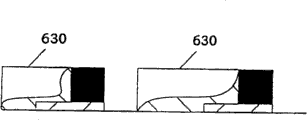
Fig. 6 (a)-6 (i) shows second embodiment of utilizing two kinds of polymer to form crosspoint array.
Fig. 7 is the flow chart of second embodiment of the method according to this invention.
Fig. 8 shows substrate and is applied by the skim photopolymer, uses the experimental result under the molded situation of ultraviolet transparent mould of PDMS subsequently.
Fig. 9 is the explanation of pattern, and wherein first aspect ratio, second feature is narrower.
Figure 10 (a)-10 (1) shows the 3rd embodiment of utilizing capillary force to form crosspoint array.
Figure 11 is the flow chart according to the 3rd embodiment of the present invention.
Embodiment
The present invention relates to a kind of method and system that is used for making semiconductor device.Following description is used to make those skilled in the art to carry out and uses patent application, and relevant application of the present invention and requirement thereof are provided.For person skilled in the art, the various corrections and the feature of preferred embodiment described herein and basic principle are conspicuous.So, the embodiment shown in the present invention is not regarded as being limited to, but give and principle described herein and the consistent maximum magnitude of feature.
As the accompanying drawing that is used to describe shown in, the present invention is a kind of method and system that is used for making semiconductor device.The present invention relates to and utilize impression tool to produce three-dimensional resist structure, thereby can in single molded step, a plurality of figure transfer be arrived resist, and in procedure of processing after a while, appeared subsequently.
Though the present invention has been described to be used to make semiconductor device, but those skilled in the art can easily understand, the present invention can be used to make the device (for example mechanical devices, optics, biological device etc.) of other type, does not still surmount design of the present invention and scope simultaneously.
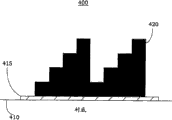
In order to understand the present invention better, can be with reference to Fig. 1.Fig. 1 is the high level flow chart of the method according to this invention.At first, provide substrate by step 110.This substrate preferably includes the flexible substrate that is suitable for roll-to-roll manufacturing process.Then, by step 120 at depositing layer of material on substrate.This material preferably includes organic material or inorganic material.At last, by step 130, form three-dimensional (3D) resist structure on first material layer, wherein the 3D resist structure comprises a plurality of different vertical heights in total.Preferably utilize coining tool to produce the 3D resist structure.Because the 3D resist structure comprises a plurality of different vertical heights in total, so structure can be used to based on subsequently corrosion step alignment patterns be transferred to the below layer.
As discussed previously, the present invention relates to and utilize impression tool on flexible substrate, to produce the 3D resist structure.In order more to be expressly understood this notion, see also Fig. 2 (a)-2 (c).Fig. 2 (a)-2 (c) shows the section that utilizes impression tool to form the 3D resist structure.Fig. 2 (a) shows the section of impression tool 210 and unfashioned anticorrosive additive material layer 214.Impression tool 210 comprises the 3D figure 212 that will be transferred to resist layer 214.Resist layer 214 can comprise any of various commercial polymer.For example, can adopt polymer from Norland optical adhesive (NOA) series of polymers.
Impression tool 210 is contacted with resist layer 214, thereby resist layer 214 is displaced in the 3D figure 212 of impression tool 210.Fig. 2 (b) shows the section of the impression tool 210 that has contacted with resist layer 214.Then, with ultraviolet lithography art or any other suitable curing, to being cured by the resist layer 214 of displacement.Fig. 2 (c) shows the section of the resist layer 214 ' of formation.
In addition, as seen, the resist layer 214 ' of formation is that resist structure comprises different vertical height 216,218,220,222 in Fig. 2 (c).Each vertical height preferably has nothing in common with each other, that is at least one is different from another height highly significantly.Therefore, these different vertical heights make that structure 214 ' can be used to based on subsequently corrosion step alignment patterns is transferred to the below layer.In the manufacturing of cross point memory array, these structures are useful especially.
Crosspoint array
Cross point memory array preferably includes two layers of separated parallel conductor quadrature group that is mounted with semiconductor layer therebetween.Two groups of conductors form the row and column electrodes, with each column electrode in the mode of accurately position and each row electrode crossing and overlapping.
In order to understand crosspoint array in more detail, see also Fig. 3.Fig. 3 is the explanation of crosspoint array structure 300.At place, each crosspoint, the semiconductor layer 330 that works by the mode of connecting with fuse with diode forms between column electrode 310 and row electrode 320 and is connected.Diode in the array all is orientated to, and all diodes will be biased along identical direction if common potential is applied between all column electrodes and all row electrodes then.Fuse element can be implemented as when critical current by the time discrete component that will open a way, maybe can be combined in the operation of diode.
Those skilled in the art can easily understand, and above-mentioned crosspoint array can be used to form various semiconductor device, including, but not limited to transistor, resistor, capacitor etc., do not surmount design of the present invention and scope simultaneously.
Propose to form the distinct methods of crosspoint array below with above-mentioned 3D resist structure.First method utilizes " sheltering " effect to form crosspoint array in conjunction with the 3D structure; The second method utilization have mutual corrosion optionally two kinds of polymer form crosspoint array; Third party's method is utilized the effect of capillary force to produce the 3D structure and is formed crosspoint array.Though described three kinds of methods, those skilled in the art can easily understand, the 3D resist structure can be utilized in conjunction with various method, does not surmount design of the present invention and scope simultaneously.
Masking effect
First method of utilizing the 3D resist structure to form crosspoint array has been considered masking effect.Masking effect is under proper condition, and when on the surface that is comprising the groove with steep sidewalls during deposition film, the material that is deposited accumulates in according to qualifications perpendicular on the surface of direction of deposition and avoid covering the phenomenon of sidewall.Deposit at a certain angle, thus " sheltering " sidewall can strengthen this effect sometimes.
In order to understand in the method, how to consider masking effect better, can be in conjunction with following description referring to Fig. 4 (a)-4 (g).Fig. 4 (a)-4 (g) shows the technology of utilizing masking effect to form crosspoint array.Fig. 4 (a) is the side view of structure 400, and this structure 400 comprises flexible substrate 410, first material layer (" the first film lamination ") 415 and the 3D resist structure 420 that forms.
In case formed resist structure, just the thin layer of removing resist structure by the anisotropy rot etching technique begins technology, thus expose portion the first film lamination.Fig. 4 (b) shows the expose portion 415 ' of the first film lamination.Then, utilize identical or different corrosion chemical methodes, the expose portion of the first film lamination is corroded, thereby forms a plurality of depressions in substrate.Fig. 4 (c) shows depression 425 and has been corroded and enters structure in the substrate 410.The sidewall that importantly caves in this technology keeps the thickness of depth ratio the first film lamination of precipitous and depression much bigger.Say ideally, in order to strengthen " sheltering " effect, if depression undercutting slightly (undercut) the first film lamination in the substrate is then best.
Then, the layer that the next one of resist structure is the thinnest is corroded, thereby exposes the second portion of the first film lamination.So the second portion of the exposure of the first film lamination is corroded.But in this step, when pellicular cascade from the substrate of its below when being eliminated, corrosion is stopped.Fig. 4 (d) shows the substrate 410 ' that is exposed after this step.
In next procedure, the thinnest part of the next one of resist structure is corroded, thereby exposes the third part of the first film lamination.But in this step, the expose portion of the first film lamination is not corroded.When finishing this step, resist originally only stays a series of isolated island.Fig. 4 (e) shows each isolated island of resist 430 and the expose portion 415 of the first film lamination ".
Then, deposit second material layer (second pellicular cascade) on total.Second pellicular cascade preferably includes semi-conducting material and electric conducting material.The small stair that the condition of these deposits will make the first film laminated thickness cause is conformally covered.But the bigger step corresponding to recessed side walls will be uncovered.Fig. 4 (f) shows second pellicular cascade 435 after the deposit.
At last, the remainder of resist structure is eliminated, thereby forms crosspoint array.Fig. 4 (g) shows the structure that comprises crosspoint array 440.Though formed crosspoint array when this step finishes, extra step can comprise slight cleaning, so that remove any residual film on the sidewall that in resulting devices, may produce short circuit.
In order to understand said method better, see also Fig. 5.Fig. 5 is the flow chart according to said method of the present invention.At first, by step 510, in case formed resist structure, the first thin layer of resist structure is just by anisotropic etch, thereby exposes the first of the first film lamination.Then, by step 520, the first of the exposure of the first film lamination is corroded, thereby forms a plurality of depressions in substrate.It is the most much bigger that the degree of depth of this depression cans be compared to most the first film lamination, and undercutting the first film lamination slightly, thereby strengthen masking effect.Then, by step 530, the second thin layer of resist is corroded, thereby exposes the second portion of the first film lamination.
Then, by step 540, the second portion of the exposure of the first film lamination is corroded.Pass through step 550, deposit second pellicular cascade then.Second pellicular cascade preferably includes semi-conducting material and electric conducting material.Equally, the small stair that the condition of these deposits will make the first film laminated thickness cause is capped, and will be uncovered corresponding to the bigger step of recessed side walls.At last, by step 560, the remainder of resist is eliminated.
Have optionally two kinds of mask polymer of mutual corrosion
Utilize the 3D resist structure to form second method of crosspoint array, two kinds of polymer have been adopted, its character makes a kind of compound can be with than being corroded under the much higher speed of another kind of compound under certain condition, for example for polymer A and B, the corrosion of polymer " A " is impact polymer " B " not, and the corrosion of polymer " B " impact polymer " A " not.These conditions can comprise different corrosion chemistry, different flow velocitys, different dividing potential drops, different plasma powers etc.In addition, these two kinds of caustic solutions preferably all are the anisotropic dry corrosion.
Though said method is disclosed as the conjugated polymer material and is utilized, but those skilled in the art are appreciated that, can can both be used to replace polymeric material by any material molded, that cast, solidify then, and not surmount design of the present invention and scope as resist.For example, spin-coating glass (SOG) can be used as second polymer in the above-mentioned embodiment of the present invention.
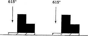
In order to understand the method better, can be in conjunction with following description referring to Fig. 6 (a)-6 (i).Fig. 6 (a)-6 (i) shows and utilizes two kinds of polymer to form the technology of crosspoint array.Fig. 6 (a) shows structure 600, and it comprises flexible substrate 610, first material layer (" the first film lamination ") and the 3D resist structure 620 that forms, and wherein exists a plurality of different vertical heights in total 620.In case formed resist structure, just remove the thinnest layer of resist structure by the anisotropy rot etching technique, thus expose portion the first film lamination.Fig. 6 (b) shows the part 615 ' that is exposed of the first film lamination.
Then, utilize identical or different corrosion chemistry, the expose portion of the first film lamination is corroded.Say that ideally these etching processs should be to remove the first film lamination to it to the similar or higher speed of the erosion rate of resist structure.Then, the layer that the next one of resist structure is the thinnest is corroded, thereby exposes the second portion of the first film lamination, wherein the zone that is corroded in the contiguous previous technology of second expose portion of the first film lamination.Fig. 6 (c) shows second expose portion 615 of the first film lamination ".
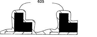
Then, deposit second material layer (second pellicular cascade).Second pellicular cascade preferably includes semi-conducting material and electric conducting material.All exposed surfaces of substrate, the first film lamination and resist can be coated in this step.Fig. 6 (d) shows second pellicular cascade 625 of deposit.
On second pellicular cascade, apply second polymer then.Can use such as intaglio printing coating roll coating process or with vacuum deposition or gas-phase deposition method, apply this coating.This coating is in order to flatten structure, and should cause smooth basically surface to cover all patterns that abovementioned steps produces.Fig. 6 (e) shows the second polymer layer 630 that covers second thin layer 625.
Then, the second polymer layer is returned corrosion, and all second pellicular cascades on the resist horizontal surface that is deposited at the beginning appear.Fig. 6 (f) shows second pellicular cascade 625 ' of the exposure after the corrosion the second polymer layer 630.Should be noted that for this technology, second pellicular cascade there is no need as etch stop layer owing to being eliminated.
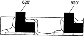
Then, second pellicular cascade is corroded from the top surface of resist structure.Etching process importantly used herein does not corrode second polymer to be higher than the speed of corroding second pellicular cascade.Fig. 6 (g) shows and corrodes second pellicular cascade resist expose portion 620 ' afterwards.Then, the thinnest zone of the next one of resist structure is corroded, thereby exposes another part of the first film lamination.Remove this part of the first film lamination then with identical or different etching processs.This group etching process that is used for removing resist and the first film lamination is not preferably removed second pellicular cascade that is covered by second polymer.Withstand the etching process of removing the first film lamination and resist by means of the top layer that makes the second polymer layer or second pellicular cascade, can reach this purpose.Fig. 6 (h) shows the remainder 630 of the second polymer layer.
At last, remove the remainder of resist structure and the second polymer layer, thereby form crosspoint array.Extra step comprises slight cleaning once more, so that remove any residual film on the sidewall that may produce short circuit in resulting devices.Fig. 6 (i) shows the structure that comprises crosspoint array 640.
In order to understand said method better, see also Fig. 7.Fig. 7 is the flow chart according to said method of the present invention.At first, by step 705, in case formed resist structure, the first thin layer of resist structure is just by anisotropic etch, thereby exposes the first of the first film lamination.Then, by step 710, the first of the exposure of the first film lamination is corroded, thus the expose portion substrate.Then, by step 715, the second thin layer of resist is corroded, thereby exposes the second portion of the first film lamination.
Then, by step 720, deposit second pellicular cascade.Second pellicular cascade preferably includes semi-conducting material and electric conducting material.By step 725, on second pellicular cascade, apply second resist layer then.Second resist layer preferably can apply by roll coating process.Then, by step 730, second resist layer is corroded, thereby exposes the first of second pellicular cascade.By step 735, this part of second pellicular cascade is corroded then.Then, by step 740, the 3rd thin layer of resist is corroded, thereby exposes the third part of the first film lamination.By step 745, this expose portion is corroded then.At last, by step 750, the remainder of resist and second resist layer are eliminated.
Capillary force
Third party's method of utilizing the 3D resist structure to form crosspoint array has been considered the capillary force phenomenon.Capillary force is to cause anticorrosive additive material to pull the power of narrow raceway groove into than entering the easier quilt of broad raceway groove.In order to understand this notion better, see also Fig. 8.
Fig. 8 shows substrate and is also used experimental result under the molded situation of ultraviolet ray (UV) transparent mould of PDMS (dimethyl silicone polymer) by the coating of photopolymer thin layer subsequently.In this example, die comprises that the degree of depth is 5.6 microns narrow (10 microns) feature and broad (100 a microns) feature.Ultraviolet solidifiable polymer foil (0.9 micron) is applied to substrate.When die contacted with liquid polymer, capillary force was pulled most polymers in the narrow raceway groove 810 into, and less polymer pulled into the zone 820 of broad.Also observe the corner district 830 that more polymer pulled into wide region 820.
In order more to be expressly understood, see also Fig. 9.Fig. 9 is the pattern explanations of first feature, 910 to the second features 920 when narrower.Because first feature, 910 to the second features 920 are narrower, so capillary force makes the polymeric material of deposit subsequently compare second feature, 920 easier first features 910 that being drawn to.As a result because first feature 910 will comprise the polymer material layer thicker than second feature 920, so below material can be according to subsequently processing step easily by graphically.
In order to understand the method better, please in conjunction with following description referring to Figure 10 (a)-10 (j).Figure 10 (a)-10 (j) has illustrated the technology of utilizing capillary force to form crosspoint array.Figure 10 (a) shows the X-X ' section (from Fig. 9) of structure, this structure comprises flexible substrate 1010, first material layer (" the first film lamination ") 1015 and the 3D resist structure 1020 that forms, and wherein exists a plurality of different vertical heights in the total 1020.Figure 10 (b) shows the Y-Y ' profile of structure.Also show feature 910 among two figure corresponding to Fig. 9 shape characteristic 910.
In case formed resist structure, just remove the thinnest layer of resist structure, thereby expose the part of the first film lamination by the anisotropy rot etching technique.Figure 10 (c) shows the X-X ' profile of structure, has wherein exposed the part 1015 ' of the first film lamination.Figure 10 (d) shows the above-mentioned etching process Y-Y ' profile of structure afterwards.
Then, deposit second material layer (second pellicular cascade).Second pellicular cascade preferably includes semi-conducting material and electric conducting material.Figure 10 (e) and 10 (f) show deposit second pellicular cascade 1030 X-X ' and the Y-Y ' profile of structure afterwards respectively.
Polymer-coated on total with second then.In coating second polymer process, two kinds of technology have been imagined.Utilize first technology, second polymer has lower viscosity and soaks into resist easily.The quantity not sufficient of second polymer of coating is present in cavity on the structure and morphology with complete filling, but because capillary force, second polymer will more easily pulled in the narrow passage.As a result, these zones will be filled into than the bigger degree of depth in zone that has bigger spacing between the sidewall.
Second technology of imagination relates to vapor deposition or vacuum deposition processes second polymer is applied structurally equably.Based on capillary force, narrow gap may crested before big gap once more.And, because this technology depends on geometric effect rather than corrosion selectivity, so second polymer can have identical with resist structure or different chemical constituents.Figure 10 (g) 10 (h) shows deposit second polymer 1040 X-X ' and the Y-Y ' profile of structure afterwards respectively.
Though said method is disclosed as the conjugated polymer material and is utilized, those skilled in the art can easily understand, and can utilize various resist compounds and do not surmount design of the present invention and scope.
In case applied second polymer, just carry out anisotropic etch, so that remove second pellicular cascade that exposes, thus expose portion first resist.Figure 10 (i) and 10 (j) show respectively and carry out the anisotropic etch X-X ' and the Y-Y ' profile of structure afterwards.Figure 10 (j) shows the resist 1020 ' of exposure.Then, remove the resist and second polymer.Second pellicular cascade covers each zone at the first film lamination place, is crosspoint array.Figure 10 (k) and 10 (l) show the X-X ' and the Y-Y ' profile of the crosspoint array 1050 of formation respectively.
In order to understand said method better, see also Figure 11.Figure 11 is the flow chart according to said method of the present invention.At first, in case formed resist structure, just carry out anisotropic etch, thereby expose the first of the first film lamination by first of the step 1100 pair resist structure the thinnest layer.The resist structure that forms preferably includes at least one feature wideer than another feature.Pass through step 1110, deposit second pellicular cascade then.Second pellicular cascade preferably includes semi-conducting material and electric conducting material.
Then, by step 1120, the deposit the second polymer layer.Carry out anisotropic etch by step 1130 then, so that remove second pellicular cascade, thus the expose portion resist.At last, by step 1140, remove the remainder of the resist and second polymer.
The method and system that is used for making semiconductor device is disclosed.The method and system relate to and utilize impression tool to produce the 3D resist structure, so that can in single molded step film pattern be transferred to resist, and are appeared in processing step after a while subsequently.
Though according to shown in each embodiment the present invention has been described, those skilled in the art can easily understand, and can carry out various changes to these embodiments, and these change all among design of the present invention and scope.Therefore, those skilled in the art can make many corrections and not depart from the design and the scope of claims.

Claims (9)

1. method that is used for making semiconductor device comprises:
Substrate [410] is provided;
Go up deposit first material layer [415] at substrate [410]; And
Go up formation three-dimensional resist structure [420] at substrate [410], wherein three-dimensional resist structure [420] comprises four different vertical heights in total [420].
2. the method for claim 1, wherein four different vertical heights comprise that at least one is different from the height of another height significantly.
3. method as claimed in claim 2, wherein, substrate [410] is a flexible substrate material, and the operation that forms three-dimensional resist structure [420] also comprises:
Go up the deposit resist layer at first material layer [415]; And
3-D graphic is transferred to resist layer, so that form three-dimensional resist structure [420].
4. method as claimed in claim 3, wherein, the operation of 3-D graphic being transferred to resist layer also comprises:
Utilize impression tool, in resist layer, form 3-D graphic; And
Resist layer is cured, thereby forms three-dimensional resist structure [440].
5. method as claimed in claim 4 also comprises:
On substrate, produce crosspoint array.
6. method as claimed in claim 5, wherein, the operation that produces crosspoint array [440] also comprises:
Anisotropic etch penetrates the first the thinnest layer of three-dimensional resist structure, thereby exposes first's [415 '] of first material layer;
Corrode first's [415 '] of the exposure of first material layer, so that form a plurality of depressions [425] in substrate [410], each of wherein a plurality of depressions [425] comprises the bigger degree of depth of thickness than first material layer [415];
Corrosion penetrates the second the thinnest layer of three-dimensional resist structure, thereby exposes the second portion of first material layer;
Corrode the second portion of the exposure of first material layer;
Corrosion penetrates the 3rd the thinnest layer of three-dimensional resist structure, thereby exposes the third part [415 "] of first material layer;
On the remainder of the expose portion of first material layer and three-dimensional resist structure, deposit second material layer [435], wherein second material layer [435] comprises semi-conducting material and electric conducting material; And
Remove the remainder of three-dimensional resist structure.
7. method as claimed in claim 5, wherein, the operation that produces crosspoint array also comprises:
Anisotropic etch penetrates the first the thinnest layer of three-dimensional resist structure, thereby exposes first's [615 '] of first material layer;
Corrode first's [615 '] of the exposure of first material layer, thereby expose a part of substrate;
Corrosion penetrates the second the thinnest layer of three-dimensional resist structure [620], thereby exposes the second portion [615 "] of first material layer;
On the remainder of the expose portion of first material layer and three-dimensional resist structure, deposit second material layer [625], wherein second material layer [625] comprises semi-conducting material and electric conducting material;
On second material layer [625], roller coating second resist layer [630], wherein the corrosion rate of second resist layer [630] is different from the corrosion rate of three-dimensional resist structure;
Corrode second resist layer [630], thereby expose first's [625 '] of second material layer;
Corrode first's [625 '] of second material layer;
Corrode the 3rd the thinnest layer of three-dimensional resist structure, thereby expose the third part of first material layer;
Corrode the third part of first material layer; And
Remove the remainder of three-dimensional resist structure and the remainder of second resist layer [625].
8. method as claimed in claim 5, wherein, three-dimensional resist structure comprises at least one raceway groove narrower than another raceway groove [910], and the operation of generation crosspoint array also comprises:
On the remainder of the expose portion [1015 '] of first material layer and three-dimensional resist structure, deposit second material layer [1030], wherein, second material layer [1030] comprises semi-conducting material and electric conducting material;
Go up deposit second resist layer [1040] at second material layer [1030], wherein, easier at least one raceway groove [910] that pulled into of second resist layer [1040];
Anisotropic etch second material layer [1030], thereby the three-dimensional resist structure of expose portion; And
Remove the remainder of three-dimensional resist structure and the remainder of second resist layer [1040].
9. method that is used for making semiconductor device, it comprises:
Flexible substrate material [410] is provided;
Go up deposit first material layer [415] in flexible substrate [410]; And
Deposit resist layer on first material layer;
Utilize impression tool, in resist layer, form 3-D graphic;
Resist layer is cured, thereby goes up formation three-dimensional resist structure [420] at first material layer [415], wherein, three-dimensional resist structure [420] comprises four different vertical heights, and wherein at least one is different from another height highly significantly; And
Utilize three-dimensional resist structure [420], go up in flexible substrate [410] and produce crosspoint array [440].
CNB031483259A 2002-06-28 2003-06-30 The manufacture method of semiconductor device and system Expired - Fee Related CN100565796C (en)

Applications Claiming Priority (2)

Application Number Priority Date Filing Date Title
US10/184567 2002-06-28
US10/184,567 US6861365B2 (en) 2002-06-28 2002-06-28 Method and system for forming a semiconductor device

Publications (2)

Publication Number Publication Date
CN1495853A CN1495853A (en) 2004-05-12
CN100565796C true CN100565796C (en) 2009-12-02

Family

ID=29717967

Family Applications (1)

Application Number Title Priority Date Filing Date
CNB031483259A Expired - Fee Related CN100565796C (en) 2002-06-28 2003-06-30 The manufacture method of semiconductor device and system

Country Status (6)

Country Link
US (1) US6861365B2 (en)
EP (1) EP1376663A3 (en)
JP (1) JP4585745B2 (en)
CN (1) CN100565796C (en)
HK (1) HK1064212A1 (en)
TW (1) TWI292588B (en)

Families Citing this family (44)

* Cited by examiner, † Cited by third party
Publication number Priority date Publication date Assignee Title
US6696220B2 (en) * 2000-10-12 2004-02-24 Board Of Regents, The University Of Texas System Template for room temperature, low pressure micro-and nano-imprint lithography
JP3821069B2 (en) 2002-08-01 2006-09-13 株式会社日立製作所 Method for forming structure by transfer pattern
US20040065252A1 (en) * 2002-10-04 2004-04-08 Sreenivasan Sidlgata V. Method of forming a layer on a substrate to facilitate fabrication of metrology standards
US7256435B1 (en) * 2003-06-02 2007-08-14 Hewlett-Packard Development Company, L.P. Multilevel imprint lithography
JP2005159294A (en) * 2003-09-18 2005-06-16 Nec Kagoshima Ltd Method of treating substrate and chemical used therefor
ATE451717T1 (en) * 2003-09-29 2009-12-15 Ibm PRODUCTION METHOD
US9039401B2 (en) 2006-02-27 2015-05-26 Microcontinuum, Inc. Formation of pattern replicating tools
US8148251B2 (en) * 2004-01-30 2012-04-03 Hewlett-Packard Development Company, L.P. Forming a semiconductor device
US7056834B2 (en) * 2004-02-10 2006-06-06 Hewlett-Packard Development Company, L.P. Forming a plurality of thin-film devices using imprint lithography
US7195950B2 (en) * 2004-07-21 2007-03-27 Hewlett-Packard Development Company, L.P. Forming a plurality of thin-film devices
US7259106B2 (en) * 2004-09-10 2007-08-21 Versatilis Llc Method of making a microelectronic and/or optoelectronic circuitry sheet
US7202179B2 (en) * 2004-12-22 2007-04-10 Hewlett-Packard Development Company, L.P. Method of forming at least one thin film device
US7521313B2 (en) * 2005-01-18 2009-04-21 Hewlett-Packard Development Company, L.P. Thin film device active matrix by pattern reversal process
US7585424B2 (en) * 2005-01-18 2009-09-08 Hewlett-Packard Development Company, L.P. Pattern reversal process for self aligned imprint lithography and device
US8097400B2 (en) * 2005-02-22 2012-01-17 Hewlett-Packard Development Company, L.P. Method for forming an electronic device
US7352376B2 (en) * 2005-03-29 2008-04-01 Hewlett-Packard Development Company, L.P. Apparatus and method for electrophoretic printing device
US7470544B2 (en) * 2005-05-26 2008-12-30 Hewlett-Packard Development Company, L.P. Sensor array using sail
US7994509B2 (en) * 2005-11-01 2011-08-09 Hewlett-Packard Development Company, L.P. Structure and method for thin film device with stranded conductor
US7533905B2 (en) * 2005-06-02 2009-05-19 Hewlett-Packard Development Company, L.P. Anti-counterfeiting system and method
US7341893B2 (en) * 2005-06-02 2008-03-11 Hewlett-Packard Development Company, L.P. Structure and method for thin film device
CN101189720A (en) * 2005-06-06 2008-05-28 Nxp股份有限公司 Method for manufacturing a crossbar circuit device
KR101107474B1 (en) * 2005-06-07 2012-01-19 엘지디스플레이 주식회사 soft mold and patterning method thereof
FR2887160B1 (en) * 2005-06-16 2007-09-14 Eastman Kodak Co METHOD FOR APPLYING A DISCONTINUOUS THIN LAYER TO A SUBSTRATE
US7678626B2 (en) * 2005-11-23 2010-03-16 Hewlett-Packard Development Company, L.P. Method and system for forming a thin film device
KR101157966B1 (en) * 2005-12-29 2012-06-25 엘지디스플레이 주식회사 Method for fabricating liquid crystal display
GB2436163A (en) * 2006-03-10 2007-09-19 Seiko Epson Corp Device fabrication by ink-jet printing materials into bank structures, and embossing tool
US7795062B2 (en) * 2007-04-03 2010-09-14 Hewlett-Packard Development Company, L.P. Method of forming a pressure switch thin film device
DE102007044505A1 (en) * 2007-09-18 2009-03-19 Robert Bosch Gmbh Process for the lithographic production of nano- and / or microstructures, stamps and substrates
US20090108397A1 (en) * 2007-10-31 2009-04-30 Warren Jackson Thin film device with layer isolation structure
US8765252B2 (en) 2007-11-30 2014-07-01 Hewlett-Packard Development Company, L.P. Thin film device with minimized spatial variation of local mean height
US8021935B2 (en) 2008-10-01 2011-09-20 Hewlett-Packard Development Company, L.P. Thin film device fabrication process using 3D template
KR20120032005A (en) * 2009-06-18 2012-04-04 휴렛-팩커드 디벨롭먼트 컴퍼니, 엘.피. Current-driven-pixel circuits and related methods
KR101549267B1 (en) * 2009-10-14 2015-09-11 엘지디스플레이 주식회사 Fabricating method of thin film transistor array substrate
KR101568268B1 (en) 2009-10-27 2015-11-11 엘지디스플레이 주식회사 Thin film transistor substrate and method of fabricating the same
US8568182B2 (en) 2010-09-27 2013-10-29 Hewlett-Packard Development Company, L.P. Display
US8877531B2 (en) 2010-09-27 2014-11-04 Applied Materials, Inc. Electronic apparatus
NL2007372C2 (en) 2011-09-08 2013-03-11 Univ Delft Tech A process for the manufacture of a semiconductor device.
GB2499606B (en) 2012-02-21 2016-06-22 Pragmatic Printing Ltd Substantially planar electronic devices and circuits
US8940555B2 (en) * 2012-09-06 2015-01-27 Globalfoundries Inc. Method and system for determining overlap process windows in semiconductors by inspection techniques
NL2010199C2 (en) 2013-01-29 2014-08-04 Univ Delft Tech Manufacturing a submicron structure using a liquid precursor.
US9589797B2 (en) 2013-05-17 2017-03-07 Microcontinuum, Inc. Tools and methods for producing nanoantenna electronic devices
KR102420081B1 (en) 2015-03-27 2022-07-13 삼성디스플레이 주식회사 Manufacturing method of thin film and manufacturing method of organic light emitting display device using the same
JP6646888B2 (en) * 2015-09-09 2020-02-14 大日本印刷株式会社 Convex structure, concave structure, and method of manufacturing convex structure
CN105425547B (en) * 2016-01-12 2018-07-10 苏州华维纳纳米科技有限公司 A kind of volume template used in exposure photo-etching and preparation method thereof

Family Cites Families (13)

* Cited by examiner, † Cited by third party
Publication number Priority date Publication date Assignee Title
JPH02156624A (en) * 1988-12-09 1990-06-15 Mitsubishi Electric Corp Manufacture of semiconductor device
JPH03100942A (en) * 1989-09-13 1991-04-25 Hitachi Chem Co Ltd Production of stamper for optical disk
JPH0580530A (en) * 1991-09-24 1993-04-02 Hitachi Ltd Production of thin film pattern
US5308415A (en) * 1992-12-31 1994-05-03 Chartered Semiconductor Manufacturing Pte Ltd. Enhancing step coverage by creating a tapered profile through three dimensional resist pull back
JP3372258B2 (en) * 1995-08-04 2003-01-27 インターナシヨナル・ビジネス・マシーンズ・コーポレーシヨン Stamps for lithography processes
EP1055260A1 (en) * 1998-02-02 2000-11-29 Uniax Corporation Organic diodes with switchable photosensitivity
US6255035B1 (en) * 1999-03-17 2001-07-03 Electron Vision Corporation Method of creating optimal photoresist structures used in the manufacture of metal T-gates for high-speed semiconductor devices
EP1072954A3 (en) * 1999-07-28 2002-05-22 Lucent Technologies Inc. Lithographic process for device fabrication
JP2001147515A (en) * 1999-09-07 2001-05-29 Ricoh Co Ltd Method for designing photomask, apparatus for designing photomask, memory medium readable with computer, photomask, photoresist, photosensitive resin, substrate, microlens and optical element
US6165911A (en) 1999-12-29 2000-12-26 Calveley; Peter Braden Method of patterning a metal layer
TW461002B (en) * 2000-06-05 2001-10-21 Ind Tech Res Inst Testing apparatus and testing method for organic light emitting diode array
CN100504598C (en) * 2000-07-16 2009-06-24 得克萨斯州大学系统董事会 High-resolution overlay alignment methods and systems for imprint lithography
JP2002162747A (en) * 2000-11-27 2002-06-07 Ricoh Opt Ind Co Ltd Manufacturing method for three-dimensional structure by multistep exposure

Also Published As

Publication number Publication date
TWI292588B (en) 2008-01-11
CN1495853A (en) 2004-05-12
HK1064212A1 (en) 2005-01-21
JP2004040092A (en) 2004-02-05
JP4585745B2 (en) 2010-11-24
TW200400542A (en) 2004-01-01
EP1376663A3 (en) 2005-04-13
US20040002216A1 (en) 2004-01-01
US6861365B2 (en) 2005-03-01
EP1376663A2 (en) 2004-01-02

Similar Documents

Publication Publication Date Title
CN100565796C (en) The manufacture method of semiconductor device and system
US8372731B2 (en) Device fabrication by ink-jet printing materials into bank structures, and embossing tool
JP2004111933A (en) Embossing mask lithography
US20090148619A1 (en) Controlling Thickness of Residual Layer
CN102707351A (en) The producing of diffraction optical element with structured glass coating
US8413576B2 (en) Method of fabricating a structure
US8895438B2 (en) Method for forming a multi-level surface on a substrate with areas of different wettability and a semiconductor device having the same
JP4466547B2 (en) Method for manufacturing transistor
US20150031185A1 (en) Methods of fabricating semiconductor devices and semiconductor devices fabricated thereby
JP6370883B2 (en) Multi-level mask circuit manufacturing and multilayer circuit
JP5090625B2 (en) Method and system for forming a semiconductor device
WO2021082981A1 (en) Nano-pattern manufacturing method, nano-imprinted substrate, and display substrate
WO2012161051A1 (en) Method for manufacturing pattern structure
TWI422085B (en) Process to produce an electronic part
KR20200004442A (en) Fluid Assembly Substrate and Manufacturing Method Thereof
CN101062494A (en) Fluid ejecting device and method for making the same
US8486514B2 (en) Method to fabricate a mould for lithography by nano-imprinting
JPH05175195A (en) Manufacture of semiconductor device
KR20150120548A (en) Roll to Roll apparatus for forming pattern and Method for forming pattern using the same
KR100301247B1 (en) Method of manufacturing a monitoring box
CN102811548B (en) Circuit structure and making method thereof
CN111446041A (en) Conductive film manufacturing method and conductive film
KR19990055771A (en) Photosensitive film formation method
JPS5961144A (en) Manufacture of semiconductor device
JPH01244645A (en) Semiconductor device and manufacture thereof

Legal Events

Date Code Title Description
C06 Publication
PB01 Publication
REG Reference to a national code

Ref country code: HK

Ref legal event code: DE

Ref document number: 1064212

Country of ref document: HK

C10 Entry into substantive examination
SE01 Entry into force of request for substantive examination
C14 Grant of patent or utility model
GR01 Patent grant
REG Reference to a national code

Ref country code: HK

Ref legal event code: GR

Ref document number: 1064212

Country of ref document: HK

ASS Succession or assignment of patent right

Owner name: APPLIED MATERIALS INC.

Free format text: FORMER OWNER: HEWLETT PACKARD CO.

Effective date: 20140903

C41 Transfer of patent application or patent right or utility model
TR01 Transfer of patent right

Effective date of registration: 20140903

Address after: California, USA

Patentee after: Applied Materials Inc.

Address before: Texas, USA

Patentee before: Hewlett-Packard Development Corp.

CF01 Termination of patent right due to non-payment of annual fee

Granted publication date: 20091202

Termination date: 20210630

CF01 Termination of patent right due to non-payment of annual fee