CN100573276C - The manufacture method of LCD and LCD - Google Patents
The manufacture method of LCD and LCD Download PDFInfo
- Publication number
- CN100573276C CN100573276C CNB2004100741433A CN200410074143A CN100573276C CN 100573276 C CN100573276 C CN 100573276C CN B2004100741433 A CNB2004100741433 A CN B2004100741433A CN 200410074143 A CN200410074143 A CN 200410074143A CN 100573276 C CN100573276 C CN 100573276C
- Authority
- CN
- China
- Prior art keywords
- liquid crystal
- partition walls
- viewing area
- crystal material
- substrates
- Prior art date
- Legal status (The legal status is an assumption and is not a legal conclusion. Google has not performed a legal analysis and makes no representation as to the accuracy of the status listed.)
- Expired - Fee Related
Links
Images


Classifications
-
- G—PHYSICS
- G02—OPTICS
- G02F—OPTICAL DEVICES OR ARRANGEMENTS FOR THE CONTROL OF LIGHT BY MODIFICATION OF THE OPTICAL PROPERTIES OF THE MEDIA OF THE ELEMENTS INVOLVED THEREIN; NON-LINEAR OPTICS; FREQUENCY-CHANGING OF LIGHT; OPTICAL LOGIC ELEMENTS; OPTICAL ANALOGUE/DIGITAL CONVERTERS
- G02F1/00—Devices or arrangements for the control of the intensity, colour, phase, polarisation or direction of light arriving from an independent light source, e.g. switching, gating or modulating; Non-linear optics
- G02F1/01—Devices or arrangements for the control of the intensity, colour, phase, polarisation or direction of light arriving from an independent light source, e.g. switching, gating or modulating; Non-linear optics for the control of the intensity, phase, polarisation or colour
- G02F1/13—Devices or arrangements for the control of the intensity, colour, phase, polarisation or direction of light arriving from an independent light source, e.g. switching, gating or modulating; Non-linear optics for the control of the intensity, phase, polarisation or colour based on liquid crystals, e.g. single liquid crystal display cells
- G02F1/133—Constructional arrangements; Operation of liquid crystal cells; Circuit arrangements
- G02F1/1333—Constructional arrangements; Manufacturing methods
- G02F1/1339—Gaskets; Spacers; Sealing of cells
- G02F1/13394—Gaskets; Spacers; Sealing of cells spacers regularly patterned on the cell subtrate, e.g. walls, pillars
-
- G—PHYSICS
- G02—OPTICS
- G02F—OPTICAL DEVICES OR ARRANGEMENTS FOR THE CONTROL OF LIGHT BY MODIFICATION OF THE OPTICAL PROPERTIES OF THE MEDIA OF THE ELEMENTS INVOLVED THEREIN; NON-LINEAR OPTICS; FREQUENCY-CHANGING OF LIGHT; OPTICAL LOGIC ELEMENTS; OPTICAL ANALOGUE/DIGITAL CONVERTERS
- G02F1/00—Devices or arrangements for the control of the intensity, colour, phase, polarisation or direction of light arriving from an independent light source, e.g. switching, gating or modulating; Non-linear optics
- G02F1/01—Devices or arrangements for the control of the intensity, colour, phase, polarisation or direction of light arriving from an independent light source, e.g. switching, gating or modulating; Non-linear optics for the control of the intensity, phase, polarisation or colour
- G02F1/13—Devices or arrangements for the control of the intensity, colour, phase, polarisation or direction of light arriving from an independent light source, e.g. switching, gating or modulating; Non-linear optics for the control of the intensity, phase, polarisation or colour based on liquid crystals, e.g. single liquid crystal display cells
- G02F1/137—Devices or arrangements for the control of the intensity, colour, phase, polarisation or direction of light arriving from an independent light source, e.g. switching, gating or modulating; Non-linear optics for the control of the intensity, phase, polarisation or colour based on liquid crystals, e.g. single liquid crystal display cells characterised by the electro-optical or magneto-optical effect, e.g. field-induced phase transition, orientation effect, guest-host interaction or dynamic scattering
- G02F1/139—Devices or arrangements for the control of the intensity, colour, phase, polarisation or direction of light arriving from an independent light source, e.g. switching, gating or modulating; Non-linear optics for the control of the intensity, phase, polarisation or colour based on liquid crystals, e.g. single liquid crystal display cells characterised by the electro-optical or magneto-optical effect, e.g. field-induced phase transition, orientation effect, guest-host interaction or dynamic scattering based on orientation effects in which the liquid crystal remains transparent
- G02F1/141—Devices or arrangements for the control of the intensity, colour, phase, polarisation or direction of light arriving from an independent light source, e.g. switching, gating or modulating; Non-linear optics for the control of the intensity, phase, polarisation or colour based on liquid crystals, e.g. single liquid crystal display cells characterised by the electro-optical or magneto-optical effect, e.g. field-induced phase transition, orientation effect, guest-host interaction or dynamic scattering based on orientation effects in which the liquid crystal remains transparent using ferroelectric liquid crystals
Abstract
In LCD, attaching components and the zone between the viewing area of attaching components inboard at the periphery that is used for sealing two substrates, setting is bonded to the one or more partition walls on two substrates, thereby reduces to be applied to the stress in the liquid crystal material.Even stress is imposed on the liquid crystal material in the periphery of substrate, partition walls also can reduce the viewing area on the opposite side that stress and stress can not be delivered to partition walls.Therefore, even because stress when in the periphery of substrate, crackle occurring, partition walls also can stop the propagation of crackle, and crackle can not enter the viewing area.
Description
Technical field
The present invention relates to the manufacture method of LCD and LCD, more specifically, relate to the LCD of the display defect that can reduce to be applied to the stress on the liquid crystal material and prevent to cause by this stress, and the manufacture method of this LCD.
Background technology
Along with the recent development of the office automation system, office automation (OA) equipment such as word processor, personal computer and PDA (personal digital assistant) is used widely.Along with popularizing of this OA equipment, bring into use to can be used in indoor and outdoor portable OA equipment, and the small size and the light weight of these equipment proposed requirement.LCD is used widely as a kind of means that can satisfy these requirements.LCD not only has small size and light weight, and has energy conservation characteristic, and replaces CRT and be used for televisor.
LCD comprises the liquid crystal material that is sealed in the gap that is formed by two substrates, and these two substrates have electrode, and these electrodes apply voltage toward each other between electrode, with the transmittance (being determined by the voltage that is applied) of control liquid crystal material.Normally used TN (twisted-nematic) liquid crystal has the response speed of Millisecond for the voltage that is applied, and this response speed drops sharply to the value near 100 milliseconds sometimes, especially in the lower scope of applying voltage.Therefore, when showing moving image (for example 60 images of per second) on the LCD of using the TN liquid crystal, thereby liquid crystal molecule can not sufficient movement makes image blurringly, so the TN liquid crystal is unsuitable for showing moving image, for example the multimedia application field.
Therefore, use and to have the spontaneous polarization phenomenon and to have dropped into practical application applying the ferroelectric liquid crystals (FLC) that voltage has microsecond level response speed or the LCD of anti ferroelectric liquid crystal (AFLC).When this liquid crystal that can high-speed response when being used for LCD, can be by be applied to the voltage on each pixel electrode by on-off element control such as TFT and MIM, and finish the polarization of liquid crystal molecule at short notice, thereby realize that excellent moving image shows.
Traditional LCD is from the white light of the back side illuminaton backlight (being made of discharge lamp or light emitting diode) of liquid crystal board, and utilizes the color filter on the liquid crystal board to realize colored the demonstration.But, if use FLC or AFLC, then because FLC or AFLC have high-speed response, therefore can carry out time-division driving (preface drives), this time-division drives by the light time of carrying out of each illuminator (for example, red, green and blue (primary colors) or green grass or young crops, pinkish red and yellow (complementary color)) is cut apart and realizes colored the demonstration.Therefore, a pixel can show the red, green and blue look, in theory, compares the demonstration that can realize three times of sharpness with the LCD of using color filter.
The layer structure that known FLC forms v-shaped structure, book-house structure or is made up of the mixing of these structures.If use FLC as liquid crystal material, then have such shortcoming: layer structure is easy to be destroyed by the stress in the liquid crystal material (for example changing the external force in gap).
Therefore, in order to resist the gap that external force keeps preset distance, use the method that between substrate, forms viscosity columnar interval body in actual applications.Fig. 1 is the schematic plan view that demonstrates traditional LCD panel.Tradition LCD panel 100 comprises by glass that has good light transmission in visible-range or quartzy array base palte that is used as a pair of insulated substrate 101 and the subtend substrate of making (counter substrate) 102.By being arranged in the 100a of viewing area to keep the gap holding element (for example, the columnar interval body) 103 of void size (gap), by the periphery of seal element 104 and closure elements 105 seal array substrates 101 and subtend substrate 102.The gap that forms by sealing is filled with the liquid crystal material 106 such as FLC.
Therefore, invented a kind of technology, by between two substrates, forming the gap that viscosity columnar interval body 103 keeps preset distance, show resistancing action not only and reducing the effect (for example, opening 8-110524 communique/1996) that external force on the gap direction but also resistancing action are increasing the external force on the gap direction referring to the spy.
But, if used viscosity columnar interval body 103, then when injecting liquid crystal, determined the volume of the liquid crystal material 106 that seals in the gap, and when temperature variation occurring, because the volume-variation in the volume change of liquid crystal material 106 and the gap that kept by columnar interval body 103 is poor, makes on the liquid crystal material 106 and is applied with stress.If form columnar interval body 103 to high-density, then owing to be provided with the viewing area of columnar interval body and be provided with the difference of linear expansion coefficient (hereinafter referred to as expansion coefficient) and elastic modulus between the periphery (interface 104a) of seal element 104, this outer part branch crackle or the defective 110 (referring to Fig. 1) that stress causes occur on predetermined direction, and defective 110 enters viewing area 100a and causes the problem that display quality descends.
For example, if use liquid crystal material: isotropic phase (Iso phase)-chiral nematic phase (N* phase)-chiral smectic phase (Sc* phase) with following phase transformation order, then by applying the consistent state of orientation that the DC electric field obtains the Sc* phase constantly in phase transformation from N* to the Sc* phase, and the volumetric contraction when supposing by phase transformation is poor, and promptly the difference of the expansion coefficient of the expansion coefficient of Sc* phase and display plate component causes defective 110.Note, the easier defective 110 that occurs when to high-density columnar interval body 103 being set, and suppose that defect level (size of defective (length), density etc.) not only depends on expansion coefficient poor of the expansion coefficient of liquid crystal material 106 and seal element 104, and depend on expansion coefficient poor of the expansion coefficient of liquid crystal material 106 and columnar interval body 103.
Because expansion coefficient and elastic modulus are the physical values that changes with environment temperature, so if in the environment that uses liquid crystal board 100, temperature variation occurred, then as mentioned above can be owing to this variation causes defective 110.For example, when driving circuit is connected to liquid crystal board 100, because the metal electrode that has used formation on the metal electrode (for example, gold) that FPC go up formed by hot press and the liquid crystal board 100 (for example, aluminium) method that couples together therefore can be owing to heat causes defective 110.Notice that defective 110 Lock-out along with the time sometimes is even but when defective 110 Lock-outs, also might cause defective 110 once more owing to the temperature variation in the environment for use of liquid crystal board 100.
Summary of the invention
The present invention is intended to overcome the above problems, an object of the present invention is to provide a kind of between two substrates, the have LCD of partition walls and the manufacture method of this LCD, the display defect that described partition walls is used for reducing the stress of liquid crystal material and therefore prevents to be caused by this stress.According to the LCD of first aspect present invention is a kind ofly be sealed in the periphery that utilizes one or more attaching components will have two substrates of electrode by the liquid crystal materials that will be made of a plurality of layers at the interface with almost parallel and bond together and constitute in the gap that forms, this LCD is characterised in that and comprises a partition walls, it is being attached in described attaching components and the zone between the viewing area of this attaching components inboard on these two substrates, and has a hole of the described liquid crystal material of guiding that is positioned at the liquid crystal injecting port side, thereby reduce to be applied to the stress on the described liquid crystal material, determine to be arranged on the position in the described hole in the partition walls according to the gradient of the layer line of described liquid crystal material, to prevent because stress and the defective that occurs along the layer line of liquid crystal material enters the viewing area, be positioned at the outside of viewing area in the wherein said a plurality of layer with one deck of the end in contact in the hole of described partition walls, and, distance X from one side of the partition walls of liquid crystal injecting port side to the viewing area satisfies: X=L/tan (θ), the normal direction distance of the L another side that to be the contact point that contacts with the layer line of liquid crystal material of the end in described hole contact with this layer line to partition walls wherein, θ be and the described another side of the layer line of the liquid crystal material of the end in contact in described hole and partition walls between angle.
In this first aspect, attaching components by being provided at the periphery that is used for sealing two substrates and be attached to two partition walls on the substrate in the zone between the viewing area of this attaching components inboard, reduced to be applied to the stress on the liquid crystal material, if and sealing is the liquid crystal materials that are made of a plurality of layer with substantially parallel interface, then partition walls is arranged so that in described a plurality of layer that the one deck with an end in contact of partition walls is positioned at the outside of viewing area.By a plurality of layers of liquid crystal material that constitutes be with almost parallel interface, for example, monostable ferroelectric liquid crystals material.When observing the plane of liquid crystal material from the top of substrate (being invisible to the naked eye certainly), align regularly with substantially parallel straight line in the interface of each layer, and this straight line (hereinafter referred to as layer line) handle by the orientation in the manufacture process in the frictional direction of alignment film and voltage apply direction and determine.This liquid crystal material has the advantages that defective (orientation defective) to occur along the layer line of liquid crystal material owing to stress.Therefore, even liquid crystal material has been subjected to stress in substrate peripheral part, this stress also can be reduced by partition walls, even and in the periphery of substrate, occurred defective along the layer line of liquid crystal material, defective can not appear in the viewing area, because the viewing area is not on the route of defective yet.
According to the LCD of second aspect present invention based on first aspect, it is characterized in that comprising the gap holding element that is used to keep two relative distances between the substrate between two substrates in the viewing area, wherein said partition walls has the expansion coefficient identical with this gap holding element.
In this second aspect, when being provided with the gap holding element that is used to keep relative distance between two substrates in the viewing area, if described partition walls and described gap holding element are to be made by the material with essentially identical expansion coefficient, then can further reduce to be applied to the stress on the liquid crystal material that is positioned at partition walls inboard (that is, in the viewing area).
Based on first aspect, it is characterized in that partition walls is lower than the bonding strength of attaching components to two substrates to the bonding strength of two substrates according to the LCD of third aspect present invention.
In this third aspect, by being provided with to such an extent that be lower than attaching components bonding strength to two substrates to the bonding strength of two substrates partition walls, the stress that is imposed on liquid crystal material by partition walls is less than by the caused stress of attaching components.Note, can regulate the bonding strength of partition walls by the width of partition walls to two substrates.
According to the LCD of fourth aspect present invention based on first aspect, it is characterized in that partition walls and attaching components are coupled together, make and between partition walls and attaching components, form a gap portion, this gap portion is in the state of being filled by the material that does not possess optical rotatory power or is in vacuum state, and the polaroid that will be in the cross Nicols state (crossed-Nicol state) is arranged on the outside surface of two substrates that comprise this gap portion.
In this fourth aspect, produce by partition walls, attaching components and two spaces (gap portion) that substrate fences up by partition walls and attaching components are coupled together, and this gap portion is under the state or vacuum state of being filled by the material that does not possess optical rotatory power.Therefore, different with the viewing area, in this gap portion, there is not optical rotatory power.In addition, because polaroid is in the cross Nicols state, therefore the light from the incident of a polaroid side can not be transmitted to another polaroid side.Therefore, the interval between partition walls and the attaching components can form shading region.
Based on first aspect, it is characterized in that except the part of viewing area periphery that according to the LCD of fifth aspect present invention partition walls is surrounded the viewing area.
Aspect the 5th, by partition walls being arranged to surround the viewing area except the part of viewing area periphery, the crackle that has reduced to occur in periphery (being included in the orientation defective in the situation of using the liquid crystal material with layer structure) enters the route of viewing area.The described part of the periphery of this display specifically refers to for injecting the bore portion that liquid crystal provides.Have in use under the situation of liquid crystal material of layer structure, if according to the layer line of this liquid crystal material bore portion is set, then defective can not enter the inboard of partition walls, and therefore almost the whole base plate district can make the viewing area.
Based on first aspect, it is characterized in that being provided with a plurality of partition walls, and these partition walls has different width according to the LCD of sixth aspect present invention.
Aspect the 6th, if LCD comprises a plurality of partition walls, width that then can be by changing each partition walls and arrange that these partition walls suitably regulate and reduce to be applied to stress on the liquid crystal material in the viewing area.For example, if make the width of lateral septal dilapidated walls wideer and the width medial septal dilapidated walls are narrower, then can with respect to the viewing area from the lateral septal dilapidated walls to the inside partition walls little by little reduce to be applied to stress the liquid crystal material, and it is basic identical with the stress that is applied to the liquid crystal material in the viewing area to be applied to the stress of the liquid crystal material in the medial septal dilapidated walls.Therefore, the layer structure of liquid crystal material can be at flip-flop at the interface.
According to the LCD manufacture method of seventh aspect present invention is to make the method that comprises with the LCD of lower part: be sealed in by bond together liquid crystal material in the gap that is constituted of the periphery that utilizes one or more attaching components will have two substrates of electrode, described liquid crystal material is made of a plurality of layers with parallel interface; And partition walls, be used for reducing to be applied to the stress of liquid crystal material, outer fix in the viewing area with electrode is between two substrates this partition walls is set, described partition walls has the hole of the described liquid crystal material of guiding that is positioned at the liquid crystal injecting port side, and determine to be arranged on the position in the described hole in the described partition walls according to the gradient of the layer line of described liquid crystal material, because stress and the defective that occurs along the layer line of liquid crystal material enters described viewing area, described method is characterised in that and may further comprise the steps to prevent: the described partition walls that will have viscosity one of is arranged in two substrates, and to be positioned at attaching components inboard but on the position in the outside, viewing area; And be set to toward each other and, partition walls be attached on two substrates from external pressurized heating by two substrates; Wherein, be positioned at the outside of described viewing area in the described a plurality of layer with one deck of the end in contact in the hole of described partition walls, and, distance X from one side of the partition walls of liquid crystal injecting port side to the viewing area is satisfied: X=L/tan (θ), the normal direction distance of the L another side that to be the contact point that contacts with the layer line of liquid crystal material of the end in described hole contact with this layer line to partition walls wherein, θ be and the described another side of the layer line of the liquid crystal material of the end in contact in described hole and partition walls between angle.
In aspect the 7th, the partition walls that will have viscosity be arranged on one of two substrates to be positioned at attaching components inboard but on the position in the outside, viewing area, and be set to toward each other and from the external pressurized heating and partition walls is attached on two substrates by two substrates.
According to the manufacture method of the LCD of eighth aspect present invention based on the 7th aspect, it is characterized in that comprising the gap holding element that is used to keep two relative distances between the substrate between two substrates of this LCD in the viewing area, and utilization and partition walls identical materials constitute this gap holding element, thereby form partition walls and gap holding element together.
In this eight aspect, because gap holding element and partition walls use identical materials to constitute together, therefore can reduce manufacturing process, boost productivity thus.
According to the present invention, owing to reduce to be applied to stress in the liquid crystal material between two substrates by the partition walls be attached on these two substrates is set, even therefore the liquid crystal material in the substrate peripheral part has been subjected to stress, also can reduce this stress by partition walls, and prevent the viewing area of Stress Transfer to the opposite side of partition walls, and in substrate peripheral part even crackle and orientation defective appear because this stress makes, also can stop the propagation of crackle and defective by partition walls.In addition, even design the ratio of the gap holding element area occupied that is provided with in the viewing area bigger than conventional value, but owing to the problem that in the viewing area, can not occur such as crackle and defective, therefore can realize gratifying display board intensity and display quality, realize having the LCD of better quality thus.In addition, because the space between partition walls and the viewing area is used as shading region, the inboard of at least one that therefore needn't be in two substrates is provided with the photomask with good shading performance, advantageous effects is provided thus, for example prevent owing to the formation photomask causes the irregular orientation defective that causes, and realize the reduction of cost.
By following detailed description, in conjunction with the accompanying drawings, can more be expressly understood the other objects and features of the invention.
Description of drawings
Fig. 1 is the schematic plan view that demonstrates traditional liquid crystal board;
Fig. 2 is the schematic plan view that demonstrates according to an example of the liquid crystal board of the embodiment of the invention 1;
Fig. 3 is the section of structure along the II-II line intercepting of Fig. 2;
Fig. 4 is the schematic plan view that demonstrates according to another example of the liquid crystal board of the embodiment of the invention 1;
Fig. 5 A to 5F is used to explain by array base palte and subtend substrate bonding are made the figure of the method for liquid crystal board together;
Fig. 6 is the schematic plan view that demonstrates according to an example of the liquid crystal board of the embodiment of the invention 2;
Fig. 7 is the schematic plan view that demonstrates according to an example of the liquid crystal board of the embodiment of the invention 3;
Fig. 8 is the schematic plan view that demonstrates according to an example of the liquid crystal board of the embodiment of the invention 4;
Fig. 9 is the schematic plan view that demonstrates according to an example of the liquid crystal board of the embodiment of the invention 5;
Figure 10 is the schematic plan view that demonstrates according to an example of the liquid crystal board of the embodiment of the invention 6;
Figure 11 is the section of structure along the XI-XI line intercepting of Figure 10;
Figure 12 is the schematic plan view that demonstrates according to an example of the liquid crystal board of the embodiment of the invention 7; And
Figure 13 is the schematic plan view that demonstrates according to another example of liquid crystal board of the present invention.
Embodiment
Following basis shows the accompanying drawing of some embodiments of the invention, and the present invention is described in detail.
(embodiment 1)
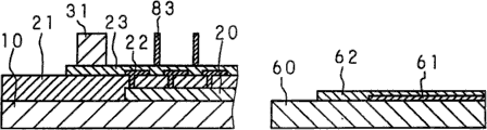
Fig. 2 is the schematic plan view that demonstrates according to an example of the liquid crystal board of the embodiment of the invention 1, and Fig. 3 is the section of structure along the II-II line intercepting of Fig. 2.For the ease of understanding, there have some parts not have to be shown in Figure 2.Liquid crystal board 1 according to the embodiment of the invention 1 comprises array base palte 10 and the subtend substrate 60 that is used as insulated substrate, and these two substrates are made by glass that has good light transmission in visible-range or quartz.Use the periphery of seal element 81 and closure elements 82 seal array substrates 10 and subtend substrate 60, the gap that forms by sealing is filled with the liquid crystal material 90 such as monostable (side is stable) ferroelectric liquid crystal material composition.
Form to constitute the TFT layer 20 of TFT matrix in the 1a of the viewing area of array base palte 10, TFT layer 20 is provided with the 2.5 μ m planarization films 21 as second interlayer dielectric such as eurymeric allyl resin (PMHD-901 that can obtain from Sumitomo Chemical Co.Ltd).In addition, the pixel electrode of being made by the ITO with good light transmission (tin indium oxide) 22 (for example, longitudinal size 130 μ m * lateral dimensions 130 μ m) is arranged to matrix form, and is connected to the drain electrode of TFT layer 20 by the contact hole that forms in planarization film 21.Note, because that base portion is preferably is smooth, so planarization film 21 has the thicker thickness of a few μ m to reduce scrambling.Therefore,, preferably in visible-range, have the material of good light transmission, thereby can not reduce the light transmission of liquid crystal board on the whole as the material of planarization film 21.In addition, by thickening planarization film 21, can reduce the stray capacitance of 20 pairs of pixel electrode 22 of TFT layer and reduce to crosstalk.
On the surface of the subtend substrate 60 relative, be formed with the counter electrode of making by ITO (or being called public electrode) 61, thereby make counter electrode 61 relative with pixel electrode 22 with good light transmission with array base palte 10.In addition, with above-mentioned array base palte 10 similarly, counter electrode 61 is coated with the alignment film 62 of thickness 20nm.For the alignment direction of the liquid crystal material 90 of determining subtend substrate 60 sides, use rayon friction matching film 62 to regulate the side chain direction.
In addition, be perpendicular to one another two polaroids 24 and 63 of crossing (being in the cross Nicols state) of polarizing axis direction are attached to respectively on the surface of array base palte 10 and subtend substrate 60, so that the direction of the polarizing axis of polaroid 24 (or 64) is alignd with the long axis direction of liquid crystal molecule.Based on the voltage that imposes on pixel electrode 22 by TFT with impose on voltage poor of counter electrode 61, the transmittance of liquid crystal material 90 among the control viewing area 1a, and the optical transmission amount sent from backlight of control are with display image.
The layer line A of liquid crystal material 90 determines by material behavior, and below hypothesis layer line A is the direction with the angled θ of frictional direction B (for example, clockwise 75 °).Partition walls 31 is made by the material with expansion coefficient identical with columnar interval body 83, and the object lesson of numerical value is 100 * 10
-6(/ ℃).Therefore, if partition walls 31 has identical expansion coefficient with columnar interval body 83, then reduce to be provided with the gap in the zone of partition walls 31 and difference between the gap among the viewing area 1a of pixel electrode 22 has been set, and reduced to be applied to the stress on the liquid crystal material 90.In addition, the width of partition walls 31 is narrower than the width of seal element 81, and the bonding strength of 31 pairs of two substrates of partition walls is littler than the bonding strength of 81 pairs of two substrates of seal element.
Below, the method that manufacturing is had the liquid crystal board 1 of said structure describes.Because the manufacture method of array base palte and subtend substrate (for example forming the method as the TFT of on-off element on array base palte) is identical with classic method, so omit explanation to it.Fig. 5 A to 5F is used to explain by array base palte and subtend substrate bonding are made the figure of the method for liquid crystal board together.
At first, on the array base palte 10 that is formed with TFT layer 20, planarization film 21 and pixel electrode 22, apply alignment film solution, subsequently 200 ℃ of bakings 30 minutes down, to form the alignment film 23 of thickness 20nm such as polyamic acid solution by spin coater.Similarly, be formed with the alignment film 62 (Fig. 5 A) that forms thickness 20nm on the subtend substrate 60 of counter electrode 61.
Next, under the display board curing condition that is deposited on the following stated on the array base palte 10, show the photosensitive resin (for example, eurymeric propenyl resist) 85 of viscosity, and in 80 ℃ of following prebake conditions 30 minutes (Fig. 5 B).Then, for between pixel electrode 22 and 22, be formed in the plan view is the columnar interval body 83 of 8 * 12 μ m rectangular shapes and in the precalculated position (sealing form district inboard) forms the partition walls 31 of wide 50 μ m, by having the exposed mask 86 irradiation 200mJ/cm of the pattern corresponding with columnar interval body 83 and partition walls 31
2Ultraviolet ray (Fig. 5 C).Afterwards, after removing unexposed portion, under 140 ℃, resin is carried out back baking 5 minutes, to form columnar interval body 83 and partition walls 31 (Fig. 5 D) by the spraying developer solution.Therefore, in the viewing area, be a bit larger tham 1% by the ratio of columnar interval body 83 area occupied.At this moment, partition walls 31 and columnar interval body 83 have the height of 2.5 μ m after back baking.Notice that partition walls 31 and columnar interval body 83 can be thermoset resin or thermoplastic resin, and needn't use identical materials partition walls 31 and columnar interval body 83.Certainly, can on the position that will form partition walls, place preformed unhardened resin thread (for example, epoxy resin line) with preset width.After this, use rayon to carry out friction treatment, to regulate the side chain direction of alignment film 23 on the array base palte 10.
On the other hand, after use rayon execution friction treatment is with the side chain direction of regulating alignment film 62 on the subtend substrate 60, on subtend substrate 60, spray spherical silica bead (particle diameter) 84 by electrostatic spray or dry shotcreting method with 1.8 μ m, and by divider with annular to the periphery part apply thermosetting seal element 81 (Fig. 5 E) under the unhardened state.Notice that seal element 81 has liquid crystal injecting port.
Next, array base palte 10 and subtend substrate 60 aimed at and carried out Vacuum Package to produce pressurized state (applying air pressure) from the outside of array base palte 10 and subtend substrate 60 by vacuum packaging machine, when keeping pressurized state, heated 90 minutes down afterwards, thereby make columnar interval body 83, partition walls 31 and seal element 81 be bonded to (Fig. 5 F) on array base palte 10 and the subtend substrate 60 at 135 ℃.At this moment, silica bead 84 is used as the auxiliary element of determining gap width, and partition walls 31 and seal element 81 are bonded on two substrates when this gap width equals the diameter of silica bead 84, so partition walls 31 and columnar interval body 83 have the height of 1.8 μ m.
Subsequently, to be heated to the chiral nematic attitude such as the liquid crystal material 90 of monostable (side is stable) ferroelectric liquid crystal material composition, and, with the UV cured resin liquid crystal injecting port is sealed afterwards by the liquid crystal injecting port injection of vacuum impregnation from the part of seal element 81.Next, make it change the chiral nematic attitude into by heating fluid eutectic substance 90, and between pixel electrode 22 and counter electrode 61, apply predetermined dc voltage (12V (electric field intensity: 5V/ μ m)) near the temperature range the transition temperature between N* phase-Sc* phase, thereby carry out after the orientation processing, liquid crystal material 90 cool to room temperature.Thus, changing to the Sc* phase time mutually, applying uniform electric field, thereby liquid crystal material 90 has consistent orientation state (layer structure) to viewing area 1a with pixel electrode 22.In addition, under the polarizing axis direction of polaroid 24 (or 63) and state that the long axis direction of liquid crystal molecule aligns, two polaroids 24 and 63 that will be in the cross Nicols state are attached to respectively on the surface of array base palte 10 and subtend substrate 60, thereby make liquid crystal board.
Next, the display quality of liquid crystal board 1 with said structure is assessed.At first, although the ratio of column interval body 83 area occupied is slightly larger than 1% in liquid crystal board 1, shown in Fig. 2 and 4, the defective 41 that is just occurred in traditional liquid crystal board can not appear in the 1a of viewing area after orientation is handled.In addition, even when carrying out temperature cycling test on liquid crystal board 1, defective 41 can not appear yet in the 1a of viewing area.
Think that its reason is as follows.By (noting in the inboard partition walls 31 that forms of seal element 81 with expansion coefficient identical with columnar interval body 83, use partition walls 31 in this case) with expansion coefficient lower than seal element 81, reduced to be applied to stress in seal element 81 liquid crystal material at the interface by partition walls 31, even and columnar interval body 83 is set with high density, partition walls 31 also can stop the propagation of the defective 41 that occurs in as the seal element 81 of starting point, therefore defective 41 can not occur in the 1a of viewing area.
(embodiment 2)
In embodiment 1, determine the position of the bore portion 31a of setting in the partition walls 31 according to the layer line A of liquid crystal material, to prevent that the defective 41 that occurs in the seal element 81 from entering viewing area 1a, but the position of bore portion 31a can be positioned at any position of liquid crystal injecting port 81a side, and embodiment 2 shows a such example.Fig. 6 is the schematic plan view that demonstrates according to an example of the liquid crystal board of the embodiment of the invention 2, and has some parts not shown in Figure 6 for ease of understanding.
According to the liquid crystal board 2 of the embodiment of the invention 2 (promptly in the inboard of seal element 81, in viewing area 2a side) have a partition walls 32, and this partition walls 32 has bore portion 32a, this bore portion 32a produces by opening is carried out at a side center of liquid crystal injecting port 81a side, so that in the liquid crystal implantation step liquid crystal material 90 is imported among the 2a of viewing area.Because other structures are identical with embodiment 1, so counterpart is represented and omission detailed description thereof with same numeral.
Next, the display quality of liquid crystal board 2 with said structure is assessed.At first, although the ratio of column interval body area occupied is slightly larger than 1% in liquid crystal board 2, as shown in Figure 6, in the 2a of viewing area, can not appear at the defective 42a and the 42b that occur after orientation is handled in traditional liquid crystal board.In addition, even carry out temperature cycling test on liquid crystal board 2, defective 42a and 42b can not appear yet in the 2a of viewing area.
Think its former because: because partition walls 32 has stoped in as the seal element 81 of starting point the defective 42a that occurs and the propagation of the defective 42a among the 42b, so in the 2a of viewing area, defective 42a can not occur.On the other hand, because partition walls 32 is not in the route of defective 42b, so can not stop the propagation of the defective 42b among defective 42a and the 42b.But, because viewing area 2a is positioned at the position more inner than the route of defective 42b, so think naturally and in the 2a of viewing area, defective 42b can not occur.
In a word, in embodiment 2, although propagating into, defective 42b is positioned at partition walls 32 area inside, owing to regulated the route of defective 42b according to the layer line A of liquid crystal material 90, so can know the route of defective 42b according to the alignment film frictional direction B of the layer line A that determines liquid crystal material 90.Therefore, owing to just can know the zone that defective can occur for certain in the stage of design liquid crystal board 2, the position that therefore can design pixel electrode 22 enters viewing area 2a to prevent defective.
(embodiment 3)
In embodiment 1 and 2, be provided with partition walls 31 and 32, but also can be for example have the partition walls of big bore portion with the shape setting of letter " C " with undersized bore portion 31a and 32a, embodiment 3 shows a such example.Fig. 7 is the schematic plan view that demonstrates according to an example of the liquid crystal board of the embodiment of the invention 3, and has some parts not shown in Figure 7 for ease of understanding.
According to the liquid crystal board 3 of the embodiment of the invention 3 (promptly in seal element 81 inboards, in viewing area 3a side) have a C shape partition walls 33, and partition walls 33 is set makes its bore portion 33a, in the liquid crystal implantation step, liquid crystal material 90 is imported viewing area 3a at liquid crystal injecting port 81a side opening.Because other structures and embodiment's 1 is identical, so counterpart is represented and omission detailed description thereof by same numeral.
Next, the display quality of liquid crystal board 3 with said structure is assessed.At first, although the ratio of column interval body area occupied is slightly larger than 1% in liquid crystal board 3, as shown in Figure 7, the defective 43a and the 43b that occur in traditional liquid crystal board can not appear in the 3a of viewing area after orientation is handled.In addition, even carry out temperature cycling test on liquid crystal board 3, defective 43a and 43b can not appear in the 3a of viewing area yet.
Think its former because: because partition walls 33 stops the defective 43a that occurs and the propagation of the defective 43a among the 43b in as the seal element 81 of starting point, so defective 43a can in the 3a of viewing area, not occur.On the other hand, because partition walls 33 is not in the route of defective 43b, so can not stop the propagation of the defective 43b among defective 43a and the 43b.But, because viewing area 3a is positioned at the position more inner than the route of defective 43b, so not think naturally and defective 43b can in the 3a of viewing area, occur.
In a word, in embodiment 3, defective 43b propagates into and is arranged in partition walls 33 area inside, but owing to regulated the route of defective 43b according to the layer line A of liquid crystal material 90, so can know the route of defective 43b according to the alignment film frictional direction B of the layer line A that determines liquid crystal material 90.Therefore, owing to just can know the zone that defective can occur for certain in the stage of design liquid crystal board 3, the position that therefore can design pixel electrode 22 enters viewing area 3a to prevent defective.
(embodiment 4)
Fig. 8 is the schematic plan view that demonstrates according to an example of the liquid crystal board of the embodiment of the invention 4, and has some parts not shown in Figure 8 for ease of understanding.
On the direction of viewing area 4a, have banded partition walls 34a and 34b according to the liquid crystal board 4 of the embodiment of the invention 4 along each long limit of seal element 81.Because other structures and embodiment's 1 is identical, so counterpart is represented and omission detailed description thereof by same numeral.
Next, the display quality of liquid crystal board 4 with said structure is assessed.At first, although the ratio of column interval body area occupied is slightly larger than 1% in liquid crystal board 4, as shown in Figure 8, defective 44a, the 44b and the 44c that occur in traditional liquid crystal board can not appear in the 4a of viewing area after orientation is handled.In addition, even carry out temperature cycling test on liquid crystal board 4, defective 44a, 44b and 44c can not appear in the 4a of viewing area yet.
Think its former because: because partition walls 34a and 34b have stoped the defective 44a, the 44b that occur and the propagation of the defective 44a among the 44c in as the seal element 81 of starting point, so defective 44a can in the 4a of viewing area, not occur.On the other hand, because partition walls 34a and 34b be not in the route of defective 44b and 44c, so can not prevent the propagation of defective 44b and 44c.But, because viewing area 4a is positioned at the position more inner than the route of defective 44b and 44c, so not think naturally and defective 44b and 44c can in the 4a of viewing area, occur.
In a word, in embodiment 4, defective 44b and 44c propagate into and are arranged in partition walls 34a and 34b area inside, but owing to regulated their route, so can know the route of defective 44b and 44c according to the alignment film frictional direction B of the layer line A that determines liquid crystal material 90 according to the layer line A of liquid crystal material 90.Therefore, owing to just can know the zone that defective can occur for certain in the stage of design liquid crystal board 4, the position that therefore can design pixel electrode 22 enters viewing area 4a to prevent defective.
Distance X 3a from the right-hand member of partition walls 34a to viewing area 4a is designed to satisfy X3a=L3/tan (θ), wherein L3 is that the layer line P3 of the liquid crystal material 90 that contacts with the right-hand member of partition walls 34a is to its normal direction distance with partition walls 34b one side of partition walls 34b intersection, promptly, relative distance between partition walls 34a and the 34b, θ is the layer line P3 of liquid crystal material 90 and the crossing angle in limit of partition walls 34a.Similarly, the distance X 3b from the left end of partition walls 34a to viewing area 4a is designed to satisfy X3b=L3/tan (θ).Therefore, even can design liquid crystal board so that occur defective 44b and 44c in actual applications, defective 44b and 44c also can be stopped in the outside of viewing area 4a and can not influence display quality.Note,, compare, also can not increase and inject the required time of liquid crystal material 90 with traditional structure even banded partition walls 34a and 34b are set.
(embodiment 5)
In embodiment 2 to 4, enter the viewing area according to the position of bore portion and the layer line A setting viewing area of liquid crystal material with the defective that prevents to occur in the seal element, but also can control the route of the defective that occurs in the seal element, and embodiment 5 shows a such example.Fig. 9 is the schematic plan view that demonstrates according to an example of the liquid crystal board of the embodiment of the invention 5, and has some parts not shown in Figure 9 for ease of understanding.
Be similar to embodiment 4, on the direction of viewing area 5a, have banded partition walls 35a and 35b along each long limit of seal element 81 according to the liquid crystal board 5 of the embodiment of the invention 5.Note, different with embodiment 4, become 75 ° direction (become with long side direction 15 ° direction) to go up friction liquid crystal board 5 at short side direction with viewing area 5a.Owing to use the liquid crystal material that between frictional direction B and layer line A, becomes 75 ° of angles, so the short side direction of viewing area 5a is parallel with layer line A.Because other structures are identical with embodiment's 1,, and omit detailed description thereof so counterpart uses same numeral to represent.
Below, the display quality of liquid crystal board 5 with said structure is assessed.At first, although the ratio of the area that the column interval body takies in liquid crystal board 5 is slightly larger than 1%, as shown in Figure 9, defective 45a, the 45b and the 45c that occur in traditional liquid crystal board can not appear in the 5a of viewing area after orientation is handled.In addition, even carry out temperature cycling test on liquid crystal board 5, defective 45a, 45b and 45c can not appear in the 5a of viewing area yet.
Think its former because: because partition walls 35a and 35b have stoped the defective 45a that occurs and the propagation of the defective 45a among the 45b in as the seal element 81 of starting point, so defective 45a can in the 5a of viewing area, not occur.On the other hand, because partition walls 35a and 35b be not in the route of defective 45b, so can not stop the propagation of defective 45b.But, because being set at, frictional direction B becomes 15 ° direction with the long side direction of liquid crystal board 5, thus think that the route of defective 45b (comprising 45a certainly) is equal to the normal direction of partition walls 35a and 35b, and defective 45b can not enter among the 5a of viewing area.
In other words, defective 45a and 45b propagate along the layer line A of liquid crystal material, but can control the route of defective 45a and 45b by control frictional direction B.In addition, in this embodiment, the whole base plate zone becomes the viewing area owing to can make basically, therefore compares with embodiment 2 to 4 and can more effectively use substrate.
Notice that embodiment 5 shows at the short side direction with viewing area 5a and becomes friction liquid crystal board 5 on 75 ° the direction, but also can become 75 ° direction (become with short side direction 15 ° direction) friction liquid crystal board 5 along long side direction with viewing area 5a.In this case, because the long side direction of viewing area 5a is parallel with layer line A, therefore partition walls can be arranged on each minor face of seal element 81.
By the way, as the semiconductor that is used for the TFT layer, mainly use amorphous silicon and polysilicon.Amorphous silicon has low mobility and is difficult to integrated driving circuit such as gate driver and Source drive, so the distance between viewing area and the periphery is generally shorter.Therefore, in the liquid crystal board of making by amorphous silicon,, preferably, adopt the structure that defective in the viewing area, do not occur described in embodiment 1 or embodiment 5 even the distance between viewing area and the periphery is shorter.
On the other hand, polysilicon has high mobility and can integrated driving circuit such as gate driver and Source drive, therefore generally driving circuit is arranged in the periphery of display board.Therefore, in the liquid crystal board of being made by polysilicon, the distance between viewing area and the periphery is longer, even therefore adopted the structure shown in the embodiment 2 to 4, does not also have too bad effect.
(embodiment 6)
Figure 10 is the schematic plan view that demonstrates according to an example of the liquid crystal board of the embodiment of the invention 6, and Figure 11 is the section of structure along the XI-XI line of Figure 10.For the ease of understanding, there have some parts not have to be shown in Figure 10.
The lower right corner that is included in two substrates 10 and 60 according to the liquid crystal board 6 of the embodiment of the invention 6 has the seal element 81 of liquid crystal injecting port 81a, and the partition walls 36 that is arranged on seal element 81 inboards.The two ends of partition walls 36 all are connected to seal element 81, and form gap portion 40 between partition walls 36 and seal element 81.This gap portion 40 is in vacuum state.In order to make gap portion 40 enter vacuum state, under vacuum, array base palte 10 and subtend substrate 60 are bonded together.Because other structures are identical with embodiment's 1, counterpart uses same numeral to represent, and omits detailed description thereof.
Therefore, owing to gap portion 40 is under the vacuum state, therefore not as viewing area 6a, in gap portion 40, there is not optical rotatory power, and,, make can not see through polaroid 24 sides from the light of polaroid 63 side incidents because polaroid 24 and 63 is in the cross Nicols state.Therefore, by gap portion 40 is set, this gap portion 40 can be used as shading region.Therefore, photomask with good light-proofness (for example Cr (chromium) or WSi needn't be set in substrate 10 or 60
2(tungsten silicide)), therefore realized the reduction of cost.And, form such metal can in the edge (interface) of photomask, cause irregular, and can be irregular and cause the orientation defective by this.But, if as among the present invention, make gap portion 40, then can not occur irregularly as shading region, and there is not the orientation defective.
(embodiment 7)
In embodiment 6, make all to be connected to the gap portion that seal element forms by two ends and to enter vacuum state, but also can fill the material that does not have optical rotatory power gap portion with partition walls, embodiment 7 shows a such example.Figure 12 is the schematic plan view that demonstrates according to an example of the liquid crystal board of the embodiment of the invention 7, has some parts not shown in Figure 12 for ease of understanding.
The lower right corner that is included in two substrates 10 and 60 according to the liquid crystal board 7 of the embodiment of the invention 7 has the first inlet 80a and has the seal element 80 of the second inlet 80b in the lower left corner, and the partition walls 37 that is positioned at seal element 80 inboards.The two ends of partition walls 37 all are connected to seal element 80.The first inlet 80a is set between substrate, to inject liquid crystal material 90, the second inlet 80b is set simultaneously between substrate, to inject the material that does not have optical rotatory power.In addition, after injecting liquid crystal material 90, use closure elements 82a to seal the first inlet 80a, after the material that will not have optical rotatory power is injected into gap portion 40, use closure elements 82b to seal the second inlet 80b.As the material that does not have optical rotatory power, for example, can use the material that does not have optical rotatory power such as gas and liquid.Because other structures are identical with embodiment's 1,, and omitted detailed description thereof so counterpart uses same numeral to represent.
Therefore, owing to filled the material that does not have optical rotatory power in the gap portion 40, so similar to Example 6, in gap portion 40,6a is different with the viewing area, owing to be in the polaroid 24 and 63 in the cross Nicols state, makes can not see through polaroid 24 sides from the light of polaroid 63 side incidents.
Notice that above-mentioned each embodiment has illustrated the situation that partition walls is made by the material with expansion coefficient identical with the columnar interval body, but the expansion coefficient of partition walls can be between the expansion coefficient of the expansion coefficient of columnar interval body and seal element.
In addition, each embodiment has illustrated the situation (being provided with two partition walls in embodiment 4) that a partition walls is set, but also a plurality of partition walls can be set between viewing area and periphery.For example, as shown in Figure 13, when being provided with three partition walls 31a, 31b and 31c, if the width of outermost partition walls 31a is W1, the width of the most inboard partition walls 31c is W3, and the width of middle partition walls 31b is W2, then preferably satisfies W1>W2>W3.Therefore, inboard partition walls has narrower width if the partition walls in the outside has the width of broad, then can be in the viewing area partition walls from the partition walls in the outside to the inboard little by little reduce to be applied to stress the liquid crystal material, and it is basic identical with the stress that imposes on the liquid crystal material in the viewing area to impose on the stress of liquid crystal material of the most inboard partition walls.Therefore, variation suddenly can not take place in the layer structure of liquid crystal material at the interface.Certainly by changing the material of partition walls but not the width that changes partition walls is regulated elastic modulus from the partition walls in outside partition walls to the inside.
In addition, in each embodiment, partition walls is formed on the planarization film.But,, also can obtain identical effect even partition walls is formed in the zone that does not constitute planarization film.
Owing under the situation of the main idea that does not break away from essential characteristic of the present invention, can implement the present invention by several forms, therefore described embodiment is illustrative rather than restrictive, because scope of the present invention is by claims but not explanation is before limited, so fall into the boundary of claim and all changes among the equivalent are included among the claim.
Claims (7)
1. LCD comprises:
Two substrates with electrode;
One or more attaching components are used for periphery with described substrate and bond to together to be formed for the gap of encapsulated liquid crystals material, and described liquid crystal material is made of a plurality of layers with parallel interface; And
A partition walls, it is being bonded in described attaching components and the zone between the viewing area of described attaching components inboard on described two substrates, and has a hole of the described liquid crystal material of guiding that is positioned at the liquid crystal injecting port side, thereby reduce to be applied to the stress on the described liquid crystal material, according to the gradient of the layer line of described liquid crystal material determine to be arranged on the position in the described hole in the partition walls, to prevent because stress and enter the viewing area along the defective that the layer line of liquid crystal material occurs
Wherein, be positioned at the outside of described viewing area in the described a plurality of layer with one deck of the end in contact in the hole of described partition walls, and, distance X from one side of the partition walls of liquid crystal injecting port side to the viewing area satisfies: X=L/tan (θ), the normal direction distance of the L another side that to be the contact point that contacts with the layer line of liquid crystal material of the end in described hole contact with this layer line to partition walls wherein, θ be and the described another side of the layer line of the liquid crystal material of the end in contact in described hole and partition walls between angle.
2. LCD according to claim 1 further comprises:
The gap holding element, it is arranged in described viewing area between described two substrates, is used to keep the relative distance between described two substrates,
The expansion coefficient of wherein said partition walls equals the expansion coefficient of described gap holding element.
3. LCD according to claim 1,
Wherein said partition walls is lower than the bonding strength of described attaching components to described two substrates to the bonding strength of described two substrates.
4. LCD according to claim 1, wherein
Described partition walls and described attaching components are connected, thereby form gap portion between described partition walls and described attaching components,
Described gap portion be in filling do not have optical rotatory power material state down or be under the vacuum state, and
The outside surface that comprises described two substrates of described gap portion is provided with the polaroid that is under the cross Nicols state.
5. LCD according to claim 1, wherein
Described partition walls is arranged to surround the described viewing area except that the part of described viewing area periphery.
6. method of making LCD, this LCD comprises: be sealed in by the periphery that will have two substrates of electrode with one or more attaching components and bond to liquid crystal material in the gap that forms together, described liquid crystal material is made of a plurality of layers with parallel interface; And partition walls, it is used to reduce to be applied to the stress on the described liquid crystal material, described partition walls at the outer fix place of the viewing area that is provided with described electrode between described two substrates, described partition walls has the hole of the described liquid crystal material of guiding that is positioned at the liquid crystal injecting port side, and according to the gradient of the layer line of described liquid crystal material determine to be arranged on the position in the described hole in the described partition walls, to prevent since stress and enter described viewing area along the defective that the layer line of liquid crystal material occurs said method comprising the steps of:
The inboard that is positioned at described attaching components in described substrate on one but be positioned on the position in the outside of described viewing area the described partition walls with viscosity is set; And
By described two substrates are positioned opposite to each other and, described partition walls is bonded on described two substrates from external pressurized heating;
Wherein, be positioned at the outside of described viewing area in the described a plurality of layer with one deck of the end in contact in the hole of described partition walls, and, distance X from one side of the partition walls of liquid crystal injecting port side to the viewing area is satisfied: X=L/tan (θ), the normal direction distance of the L another side that to be the contact point that contacts with the layer line of liquid crystal material of the end in described hole contact with this layer line to partition walls wherein, θ be and the described another side of the layer line of the liquid crystal material of the end in contact in described hole and partition walls between angle.
7. the method for manufacturing LCD according to claim 6, wherein
Described LCD comprises the gap holding element between described two substrates of described viewing area, this gap holding element is used to keep the relative distance between described two substrates, and
Use with described partition walls identical materials and form described gap holding element, thereby form described partition walls and described gap holding element together.
Applications Claiming Priority (2)
| Application Number | Priority Date | Filing Date | Title |
|---|---|---|---|
| JP2004105453A JP4480443B2 (en) | 2004-03-31 | 2004-03-31 | Liquid crystal display device and method of manufacturing liquid crystal display device |
| JP2004105453 | 2004-03-31 |
Publications (2)
| Publication Number | Publication Date |
|---|---|
| CN1677196A CN1677196A (en) | 2005-10-05 |
| CN100573276C true CN100573276C (en) | 2009-12-23 |
Family
ID=35049798
Family Applications (1)
| Application Number | Title | Priority Date | Filing Date |
|---|---|---|---|
| CNB2004100741433A Expired - Fee Related CN100573276C (en) | 2004-03-31 | 2004-08-31 | The manufacture method of LCD and LCD |
Country Status (5)
| Country | Link |
|---|---|
| US (1) | US7362404B2 (en) |
| JP (1) | JP4480443B2 (en) |
| KR (1) | KR100662067B1 (en) |
| CN (1) | CN100573276C (en) |
| TW (1) | TWI300505B (en) |
Families Citing this family (37)
| Publication number | Priority date | Publication date | Assignee | Title |
|---|---|---|---|---|
| TWI306530B (en) * | 2003-10-01 | 2009-02-21 | Himax Tech Inc | Liquid crystal display panel and liquid crystal on silicon display panel |
| JP2005257883A (en) * | 2004-03-10 | 2005-09-22 | Nec Lcd Technologies Ltd | Liquid crystal display device |
| JP4389780B2 (en) | 2004-12-27 | 2009-12-24 | セイコーエプソン株式会社 | Method for manufacturing liquid crystal device, liquid crystal device, and electronic apparatus |
| TWI271591B (en) * | 2005-01-31 | 2007-01-21 | Au Optronics Corp | Liquid crystal display and fabrication method thereof |
| KR101146536B1 (en) * | 2005-06-27 | 2012-05-25 | 삼성전자주식회사 | Display panel, method of manufacturing the same and display device having the same |
| JP5066836B2 (en) * | 2005-08-11 | 2012-11-07 | セイコーエプソン株式会社 | Electro-optical device and electronic apparatus |
| KR20070025447A (en) * | 2005-09-02 | 2007-03-08 | 삼성전자주식회사 | Liquid crystal display and method for manufacturing the same |
| JP5382395B2 (en) * | 2006-01-23 | 2014-01-08 | セイコーエプソン株式会社 | Electrophoretic display sheet, electrophoretic display device, and electronic apparatus |
| US20070178618A1 (en) * | 2006-01-31 | 2007-08-02 | Chunghwa Picture Tubes, Ltd. | Method for manufacturing liquid crystal display panel |
| TWI337285B (en) * | 2006-04-25 | 2011-02-11 | Au Optronics Corp | Active device array substrate, color filter substrate and respective manufacturing methods thereof |
| WO2008056787A1 (en) * | 2006-11-10 | 2008-05-15 | Asahi Glass Company, Limited | Method for manufacturing liquid crystal display and liquid crystal display |
| JP4910672B2 (en) * | 2006-12-12 | 2012-04-04 | ソニー株式会社 | Display module, display device, and electronic device |
| US7733559B2 (en) | 2006-12-28 | 2010-06-08 | Seiko Epson Corporation | Electrophoretic display sheet, electrophoretic display device, and electronic apparatus |
| JP4978248B2 (en) * | 2007-03-14 | 2012-07-18 | 三菱電機株式会社 | Liquid crystal display device and manufacturing method thereof |
| US7815480B2 (en) * | 2007-11-30 | 2010-10-19 | Corning Incorporated | Methods and apparatus for packaging electronic components |
| FR2934061B1 (en) * | 2008-07-15 | 2010-10-15 | Commissariat Energie Atomique | LIQUID CRYSTAL ALIGNMENT LAYER DEPOSITED AND FRICTED BEFORE REALIZING THE MICROSTRUCTURES |
| JP5357730B2 (en) * | 2009-12-15 | 2013-12-04 | 株式会社ジャパンディスプレイ | Liquid crystal display device and manufacturing method thereof |
| JP4999127B2 (en) * | 2010-06-18 | 2012-08-15 | 株式会社ジャパンディスプレイセントラル | Liquid crystal display |
| KR20120004862A (en) * | 2010-07-07 | 2012-01-13 | 삼성모바일디스플레이주식회사 | Organic light emitting diode display |
| JP5731284B2 (en) | 2011-06-02 | 2015-06-10 | ピクストロニクス,インコーポレイテッド | Display device and manufacturing method thereof |
| JP5408373B2 (en) * | 2012-08-17 | 2014-02-05 | 旭硝子株式会社 | ELECTRONIC DEVICE MEMBER, ELECTRONIC DEVICE MANUFACTURING METHOD, AND ELECTRONIC DEVICE MEMBER |
| US9122047B2 (en) * | 2012-12-31 | 2015-09-01 | Pixtronix, Inc. | Preventing glass particle injection during the oil fill process |
| CN103984154A (en) * | 2013-12-25 | 2014-08-13 | 上海天马微电子有限公司 | Display panel, manufacturing method thereof and display device |
| WO2015168782A1 (en) * | 2014-05-05 | 2015-11-12 | Lensvector Inc. | Method of wafer scale fabrication and assembly of a liquid crystal electro-optic device |
| CN104656293B (en) * | 2015-03-18 | 2017-11-28 | 合肥京东方光电科技有限公司 | Liquid crystal display panel and preparation method thereof, display device |
| US20170010630A1 (en) * | 2015-07-22 | 2017-01-12 | Boe Technology Group Co., Ltd. | Touch Display Screen, Method for Preparing Touch Display Screen and Attaching Adhesive Jig |
| CN105183209B (en) * | 2015-07-22 | 2019-05-03 | 合肥鑫晟光电科技有限公司 | Touch display screen and preparation method thereof and joint adhesive jig |
| US20170026553A1 (en) * | 2015-07-24 | 2017-01-26 | Apple Inc. | Displays With Camera Window Openings |
| JP2017111290A (en) * | 2015-12-16 | 2017-06-22 | 株式会社ジャパンディスプレイ | Liquid crystal display device |
| KR102516055B1 (en) | 2016-07-05 | 2023-03-31 | 삼성디스플레이 주식회사 | flexible display device |
| JP2018205358A (en) | 2017-05-30 | 2018-12-27 | 株式会社ジャパンディスプレイ | Display |
| JP2019066532A (en) | 2017-09-28 | 2019-04-25 | シャープ株式会社 | Optical shutter for camera module and method for manufacturing the same |
| US11105677B2 (en) * | 2017-11-06 | 2021-08-31 | Apple Inc. | Electronic devices with switchable diffusers |
| JP7058534B2 (en) * | 2018-03-27 | 2022-04-22 | シチズンファインデバイス株式会社 | LCD panel |
| CN109752889B (en) * | 2019-03-26 | 2021-01-01 | 深圳市华星光电技术有限公司 | Liquid crystal display panel |
| KR20210021210A (en) * | 2019-08-16 | 2021-02-25 | 삼성디스플레이 주식회사 | Display device |
| CN114361361B (en) * | 2021-12-31 | 2024-02-09 | 武汉天马微电子有限公司 | Display panel and display device |
Family Cites Families (27)
| Publication number | Priority date | Publication date | Assignee | Title |
|---|---|---|---|---|
| JPS60212733A (en) * | 1984-04-06 | 1985-10-25 | Hitachi Ltd | Liquid crystal display element |
| JPS63137213A (en) | 1986-11-29 | 1988-06-09 | Toppan Printing Co Ltd | Liquid crystal display element |
| JPH02126231A (en) * | 1988-11-05 | 1990-05-15 | Sharp Corp | Liquid crystal display element |
| JPH05119325A (en) * | 1991-10-24 | 1993-05-18 | Fujitsu Ltd | Liquid crystal panel |
| JP2861757B2 (en) | 1992-11-10 | 1999-02-24 | 三菱電機株式会社 | Electrode device for vacuum valve |
| JPH07318912A (en) * | 1993-07-22 | 1995-12-08 | Toppan Printing Co Ltd | Liquid crystal panel frame, liquid crystal panel body and liquid crystal display |
| JPH07128640A (en) * | 1993-10-29 | 1995-05-19 | Sharp Corp | Ferroelectric liquid crystal display device |
| US5517344A (en) * | 1994-05-20 | 1996-05-14 | Prime View Hk Limited | System for protection of drive circuits formed on a substrate of a liquid crystal display |
| JP3572550B2 (en) | 1994-10-07 | 2004-10-06 | 富士通株式会社 | Optical switch element and method of manufacturing the same |
| SE503136C2 (en) * | 1994-12-09 | 1996-04-01 | Emt Ag | Pressure resistant liquid crystal cell |
| JPH10268361A (en) * | 1997-03-27 | 1998-10-09 | Semiconductor Energy Lab Co Ltd | Liquid crystal display device and its manufacture |
| JP3456896B2 (en) | 1997-12-25 | 2003-10-14 | シャープ株式会社 | Liquid crystal display |
| JP2000066176A (en) * | 1998-08-19 | 2000-03-03 | Toppan Printing Co Ltd | Liquid crystal panel body |
| JP2000137236A (en) | 1998-10-30 | 2000-05-16 | Hitachi Ltd | Liquid crystal display element and its production |
| TW440738B (en) | 1999-12-27 | 2001-06-16 | Ind Tech Res Inst | A structure of multi-domain liquid crystal display |
| JP2002023164A (en) | 2000-07-04 | 2002-01-23 | Nec Corp | Method for liquid crystal displaying, liquid crystal display device and device for manufacturing the same |
| JP4609679B2 (en) * | 2000-07-19 | 2011-01-12 | 日本電気株式会社 | Liquid crystal display |
| JP2003057660A (en) * | 2001-06-05 | 2003-02-26 | Sharp Corp | Liquid crystal display element and liquid crystal display device using the same |
| JP4081643B2 (en) * | 2001-08-01 | 2008-04-30 | 株式会社日立製作所 | Liquid crystal display |
| JP2003140183A (en) * | 2001-08-22 | 2003-05-14 | Sharp Corp | Reflective liquid crystal display device |
| KR100685949B1 (en) * | 2001-12-22 | 2007-02-23 | 엘지.필립스 엘시디 주식회사 | A Liquid Crystal Display Device And The Method For Manufacturing The Same |
| JP3937304B2 (en) * | 2002-01-10 | 2007-06-27 | 鹿児島日本電気株式会社 | Manufacturing method of liquid crystal display panel |
| KR100453897B1 (en) | 2002-01-15 | 2004-10-20 | 삼성에스디아이 주식회사 | Raw panel for liquid crystal display and manufacturing method of color liquid crsytal display using the raw panel |
| JP2003315810A (en) | 2002-02-20 | 2003-11-06 | Hitachi Displays Ltd | Liquid crystal display panel |
| KR100867167B1 (en) | 2002-06-17 | 2008-11-06 | 엘지디스플레이 주식회사 | Liquid Crystal Display Device and Method for Fabricating the same |
| JP4059735B2 (en) | 2002-09-03 | 2008-03-12 | 株式会社 日立ディスプレイズ | Liquid crystal display |
| US20040160566A1 (en) * | 2003-02-17 | 2004-08-19 | Shinichi Kawabe | Liquid crystal display panel with fluid control wall |
-
2004
- 2004-03-31 JP JP2004105453A patent/JP4480443B2/en not_active Expired - Fee Related
- 2004-08-23 TW TW093125342A patent/TWI300505B/en not_active IP Right Cessation
- 2004-08-30 KR KR1020040068625A patent/KR100662067B1/en not_active IP Right Cessation
- 2004-08-31 CN CNB2004100741433A patent/CN100573276C/en not_active Expired - Fee Related
- 2004-08-31 US US10/930,529 patent/US7362404B2/en not_active Expired - Fee Related
Also Published As
| Publication number | Publication date |
|---|---|
| CN1677196A (en) | 2005-10-05 |
| US7362404B2 (en) | 2008-04-22 |
| US20050219456A1 (en) | 2005-10-06 |
| TWI300505B (en) | 2008-09-01 |
| KR20050096806A (en) | 2005-10-06 |
| JP4480443B2 (en) | 2010-06-16 |
| JP2005292347A (en) | 2005-10-20 |
| TW200532320A (en) | 2005-10-01 |
| KR100662067B1 (en) | 2006-12-27 |
Similar Documents
| Publication | Publication Date | Title |
|---|---|---|
| CN100573276C (en) | The manufacture method of LCD and LCD | |
| KR100220550B1 (en) | Liquid crystal display panel and liquid crystal display device | |
| JP3624834B2 (en) | Electro-optical panel, projection display device, and method of manufacturing electro-optical panel | |
| US5757451A (en) | Liquid crystal display device spacers formed from stacked color layers | |
| US7180566B2 (en) | Liquid crystal display device and repairing method thereof | |
| CN1991531B (en) | Liquid crystal display panel and method of manufacturing the same | |
| JPH08271871A (en) | Display device | |
| JPH08201830A (en) | Liquid crystal display device | |
| JP3083717B2 (en) | Liquid crystal display panel and liquid crystal display device using the same | |
| CN101613177A (en) | Scoring equipment and adopt this scoring equipment to make the method for display panel | |
| TWI400526B (en) | Substrate for a liquid crystal display device and liquid crystal display device having the same | |
| JP2000019528A (en) | Liquid crystal display device | |
| US20080094564A1 (en) | Liquid crystal display device and method for manufacturing the same | |
| KR100604036B1 (en) | Method of manufacturing of liquid crystal cell using UV curable liquid crystal | |
| KR101289064B1 (en) | Fabrication method of liquid crystal display device | |
| JP2003066465A (en) | Liquid crystal device and manufacturing method therefor | |
| JPH08220552A (en) | Liquid crystal display panel and liquid crystal display devic | |
| KR101128464B1 (en) | Liquid crystal display panel and method of fabricating the same | |
| JP2001201752A (en) | Optoelectronic panel, production type display device and method of producing optoelectronic panel | |
| KR20050090035A (en) | Liquid crystal display panel and the method of therof | |
| JPH08129181A (en) | Liquid crystal display device | |
| KR101192785B1 (en) | Liquid Crystal Display Device and Method of fabricating the same | |
| KR100862072B1 (en) | liquid crystal panel including step compensated pattern | |
| KR20030094849A (en) | Method for fabricating of liquid crystal display device | |
| JP2004213048A (en) | Electrooptic panel, projection display device, and method for manufacturing electrooptic panel |
Legal Events
| Date | Code | Title | Description |
|---|---|---|---|
| C06 | Publication | ||
| PB01 | Publication | ||
| C10 | Entry into substantive examination | ||
| SE01 | Entry into force of request for substantive examination | ||
| C14 | Grant of patent or utility model | ||
| GR01 | Patent grant | ||
| CF01 | Termination of patent right due to non-payment of annual fee |
Granted publication date: 20091223 Termination date: 20150831 |
|
| EXPY | Termination of patent right or utility model |