CN100576595C - Light-emitting device - Google Patents
Light-emitting device Download PDFInfo
- Publication number
- CN100576595C CN100576595C CN03158666A CN03158666A CN100576595C CN 100576595 C CN100576595 C CN 100576595C CN 03158666 A CN03158666 A CN 03158666A CN 03158666 A CN03158666 A CN 03158666A CN 100576595 C CN100576595 C CN 100576595C
- Authority
- CN
- China
- Prior art keywords
- film
- light
- forms
- inorganic insulating
- electrode
- Prior art date
- Legal status (The legal status is an assumption and is not a legal conclusion. Google has not performed a legal analysis and makes no representation as to the accuracy of the status listed.)
- Expired - Fee Related
Links
Images


Classifications
-
- H—ELECTRICITY
- H10—SEMICONDUCTOR DEVICES; ELECTRIC SOLID-STATE DEVICES NOT OTHERWISE PROVIDED FOR
- H10K—ORGANIC ELECTRIC SOLID-STATE DEVICES
- H10K50/00—Organic light-emitting devices
- H10K50/80—Constructional details
- H10K50/84—Passivation; Containers; Encapsulations
- H10K50/842—Containers
- H10K50/8426—Peripheral sealing arrangements, e.g. adhesives, sealants
-
- H—ELECTRICITY
- H10—SEMICONDUCTOR DEVICES; ELECTRIC SOLID-STATE DEVICES NOT OTHERWISE PROVIDED FOR
- H10K—ORGANIC ELECTRIC SOLID-STATE DEVICES
- H10K50/00—Organic light-emitting devices
- H10K50/80—Constructional details
- H10K50/84—Passivation; Containers; Encapsulations
- H10K50/844—Encapsulations
-
- H—ELECTRICITY
- H10—SEMICONDUCTOR DEVICES; ELECTRIC SOLID-STATE DEVICES NOT OTHERWISE PROVIDED FOR
- H10K—ORGANIC ELECTRIC SOLID-STATE DEVICES
- H10K50/00—Organic light-emitting devices
- H10K50/80—Constructional details
- H10K50/87—Arrangements for heating or cooling
-
- H—ELECTRICITY
- H10—SEMICONDUCTOR DEVICES; ELECTRIC SOLID-STATE DEVICES NOT OTHERWISE PROVIDED FOR
- H10K—ORGANIC ELECTRIC SOLID-STATE DEVICES
- H10K59/00—Integrated devices, or assemblies of multiple devices, comprising at least one organic light-emitting element covered by group H10K50/00
- H10K59/10—OLED displays
- H10K59/12—Active-matrix OLED [AMOLED] displays
Abstract
The problem of the release heat that produces when the objective of the invention is to solve film (polytetrafluoroethylene (R)) that above-mentioned use contains fluororesin, and the problem that solves the metallic material corrosion that causes because of fluorine element as the diaphragm of element.Therefore, the present invention adopts after forming element and forms inorganic insulating membrane, form the laminated construction of the film that contains fluororesin at last, so just make the film that contains fluororesin not contact and form, thereby reach the purpose that prevents to cause metallic material corrosion because of the fluorine element in the film that contains fluororesin with the metal material of element.Inorganic insulating membrane has the function (being block) that fluorine element in the film that prevents to contain fluororesin and metal material react.And this inorganic insulating membrane adopts the material of high-termal conductivity to form so that the heat that releasing member produces.
Description
Technical field
The present invention relates to have the manufacture method of the light-emitting device and this light-emitting device of light-emitting component, wherein the element of the film (hereinafter referred to as organic compound layer) by containing organic compound to clamping between pair of electrodes applies electric field, makes light-emitting component emitting fluorescence or phosphorescence.Concrete, the present invention relates to a kind of technology, this technology realizes protecting the above-mentioned light-emitting component that forms on component substrate not to be subjected to the influence of moisture or oxygen by using the film of being made by fluororesin.In the present technique explanation, the term light-emitting device is meant image display device, light-emitting device or the light source (comprising lighting device) that uses light-emitting component.And, following module is included in the light-emitting device: be mounted with connector at light-emitting component, such as the module of FPC (flexible print circuit), TAB (band engages (tape automatedbonding) automatically) band or TCP (being with delivery bag (tape carrier package)); Be mounted with the module of printed substrate in the termination of TAB band or TCP; Or IC (integrated circuit) directly is installed to module on the light-emitting component by COG (glass top chip) mode.
Background technology
The material that use has thin thickness, in light weight, features such as response is fast, low voltage DC driving is applied in the flat-panel monitor of future generation by expectation as the light-emitting component of luminous element.In addition, because wide visual angle and good visibility, the light-emitting device that its interior light-emitting component is arranged in the matrix configuration is considered to more have superiority than the liquid crystal display device of routine.
It is said that light-emitting component is luminous by following mechanism: just, when voltage is applied to the electroluminescent layer that is clipped between the pair of electrodes, be compounded to form molecular excitation mutually at the luminescence center of electroluminescent layer by the negative electrode injected electrons with by anode injected electrons hole.Subsequently, when molecular excitation is returned ground state, take place luminous by releasing energy.Be known in the art two types excitation state, be excited singlet state and be excited triplet.Can think and to realize luminous through any state of two types.
But light-emitting device in the mill and other display unit such as for example liquid crystal indicator has different problems.
The known luminescence element is owing to moisture is degenerated, concrete, because the influence of moisture, cause that generation is peeled off or caused that the material that forms electroluminescent layer is rotten between electroluminescent layer and electrode, so produce the non-light-emitting area that is called as blackspot, or the generation light-emitting area dwindles so that can not keep predetermined luminous problem.Notice that the degeneration of above-mentioned light-emitting component when long-time driving element, can make the reliability of element reduce.
As solution to the problems described above, knownly on element, form the technology (for example, with reference to patent document 1) that polytetrafluoroethylene (R) the AF film (du pont company manufacturing) of polytetrafluoroethylene (R) base polymer comes potted component with vapour deposition.But, though adopting polytetrafluoroethylene (R) can make relative dielectric constant is 1.9~2.1, but there are the thermal stability of polytetrafluoroethylene (R) and metal and fluorine element to produce problems such as reaction, so as on element, directly forming these films, can cause to be released in the heat that produces in the element, and the problem that forms metal material (electrode or lead-in wire etc.) the generation corrosion of element.
Patent document 1
JP?Hei?2-409017
Summary of the invention
So, produce the problem that discharges heat when the objective of the invention is to solve film (polytetrafluoroethylene (R)) that above-mentioned use contains fluororesin, and solve the problem that causes metallic material corrosion because of fluorine element as the diaphragm of element.
In order to address the above problem, the present invention adopts after forming element and forms inorganic insulating membrane, form the laminated construction of the film that contains fluororesin then, so just can form the film that contains fluororesin and it is not contacted with the metal material of element, thereby reach the purpose that prevents the metallic material corrosion that causes because of the fluorine element in the film that contains fluororesin.
Among the present invention, be formed on the metal film (second electrode) of element and contain inorganic insulating membrane between the film of fluororesin and have the function (being block) that fluorine element in the film that prevents to contain fluororesin and described metal material react.And this inorganic insulating membrane adopts the material of high-termal conductivity to form so that the heat that releasing member produces.Inorganic insulating membrane can adopt particularly and pass through sputtering method, CVD method or vapour deposition and the inorganic insulating material that obtains are such as silicon nitride, nitride-monox (SiNxOy), silica, aluminium nitride (AlN), oxidation aluminium nitride (AlNxOy), DLC (diamond-like-carbon) film, carbon nitride films (CxNy) etc.
Concrete structure of the present invention is: a kind of light-emitting device: have and comprise first electrode, the electroluminescent film that forms on described first electrode, and the light-emitting component of second electrode that forms on described electroluminescent film is characterized in that comprising:
The inorganic insulating membrane that contact forms on described second electrode;
And the film that contains fluororesin that on described inorganic insulating membrane, forms.
The film that contains fluororesin in the said structure contacts and forms with inorganic insulating membrane, and wherein inorganic insulating membrane is the metal material (i.e. second electrode) that is covered with element and forming, and therefore, has the function that prevents that light-emitting component from degenerating because of moisture and oxygen.
The present invention can use by polytetrafluoroethylene, tetrafluoraoethylene-hexafluoropropylene copolymer (tetrafluoroethylene-hexafluoropropylene copolymer), polychlorotrifluoroethylene (is abbreviated as PCTFE, Polychlorotrifluoroethylene), tetrafluoroethylene-ethylene copolymer (tetrafluoroethylene-ethylene copolymer), polyvinyl fluoride (is abbreviated as PVF, Poly vinyl fluoride), Kynoar (is abbreviated as PVDF, Polyvinylidene Fluoride) etc. the target of making forms the film that contains these fluororesin by sputtering method, has promptly formed the film that contains fluororesin of the present invention.
Be positioned at the seal substrate on the described film that contains fluororesin, between described seal substrate and the described film that contains fluororesin, has the space, wherein, by described seal substrate being pasted described substrate, make described light-emitting component, described inorganic insulating membrane and the described film that contains fluororesin sealed with encapsulant.
Except said structure, the present invention can also form the organic insulating film of being made by organic insulating material on inorganic insulating membrane, then its surface is implemented the operation of planarization, forms the film that contains fluororesin at last.
And except said structure, the present invention can also be following structure, promptly goes up at inorganic insulating membrane (first dielectric film) and forms organic insulating film, forms inorganic insulating membrane (second dielectric film) afterwards once more, forms the film that contains fluororesin then.
In above-mentioned each structure, above-mentioned organic insulating film can be by acrylic acid, polyamide, any formation in the polyimides.
Other structures among the present invention are: a kind of light-emitting device: have comprise that intermediary's dielectric film and the TFT that forms have first electrode of electrical connection on substrate, the electroluminescent film that on described first electrode, forms, and the light-emitting component of second electrode that on described electroluminescent film, forms, it is characterized in that comprising:
The inorganic insulating membrane that contact forms on described second electrode;
And the film that contains fluororesin that contact forms on described inorganic insulating membrane;
Be positioned at the seal substrate on the described film that contains fluororesin, between described seal substrate and the described film that contains fluororesin, has the space, wherein by described seal substrate being pasted described substrate, make described light-emitting component, described inorganic insulating membrane and the described film that contains fluororesin sealed with encapsulant.
According to above-mentioned structure, with containing the diaphragm of the film of fluororesin, can obtain to be released in the function of the heat that produces in the element as element, simultaneously, can not cause Corrosion of Metallic Materials because of fluorine element.
The film that contains fluororesin that forms with sputtering method of the present invention can be applied to the surface (promptly and extraneous air, the surface that staff etc. contact) of light-emitting device and other manufactured goods
Description of drawings
Fig. 1 is the structure key diagram of light-emitting device of the present invention;
Fig. 2 is the structure key diagram of light-emitting device of the present invention;
Fig. 3 is the structure key diagram of light-emitting device of the present invention;
Fig. 4 A and 4B are respectively the hermetically-sealed construction key diagrams about light-emitting device of the present invention;
Fig. 5 A~5H illustrates the example of the concrete electronic equipment of using light-emitting device of the present invention respectively;
Fig. 6 represents the result about the film that contains fluororesin that measures with ESCA;
Fig. 7 represents the result about the film that contains fluororesin that measures with ESCA;
Fig. 8 represents the result about the film that contains fluororesin that measures with IR.
The explanation of symbol
101 first substrates;
102 (the dielectric films of 102a~102c);
103TFT; 104 gate electrodes; 105 channel formation regions;
106 impurity ranges;
107 lead-in wires;
108 first electrodes;
109 insulants;
110 electroluminescent layers; 111 second electrodes; 112 inorganic insulating membranes;
113 contain the film of fluororesin
Embodiment
Embodiment pattern 1
In the present embodiment pattern 1, after light-emitting component forms, hereinafter will just on second electrode, form by exothermicity being arranged and fluorine element being had the inorganic insulating membrane of barrier effect and have and prevent that moisture and oxygen from invading the situation of the lamination that the film that contains fluororesin of function constitutes, be elaborated with Fig. 1.
Note, in the present invention, the structure of light-emitting device can adopt 2 kinds of structures, promptly the light that produces at light-emitting component is formed with bottom surface emission type structure that the side of the component substrate of TFT launches and the end face emission type structure of launching from the opposing face of component substrate at the light that light-emitting component produces from it.Put up with in the embodiment pattern 1 and adopt the situation of end face emission type structure to describe.
Fig. 1 is the part that a sectional view illustrates pixel portion.In Fig. 1,101 is first substrates, 102a, 102b and 102c are insulating barriers, the 103rd, TFT (it comprises gate electrode 104, channel formation region territory 105, impurity range 106), the 107th, lead-in wire, 108 is first electrodes, the 109th, and insulant, the 110th, electroluminescent layer, 111 is second electrodes, the 112nd, and inorganic insulating membrane and 113 is the films that contain fluororesin.
At first, the insulating barrier 102a (herein for as the insulative nitride film of lower floor with as the stack membrane of the insulation oxide film on upper strata) that is used for end insulation film forms on first substrate 101.Insulating barrier 102b as gate insulating film is provided between the gate electrode 104 and active layer of TFT.In addition, form the insulating barrier 102c of interlayer dielectric on gate electrode 104, this insulating barrier is made by organic material or inorganic material.
In addition, the TFT103 (using p channel-type TFT herein) that contacts with insulating barrier 102a and form on first substrate 101 is the element that control flows is gone into the electric current of electroluminescent layer 110.The 106th, impurity range (source region or drain region).In addition, the 107th, be used for first electrode 108 is connected to the lead-in wire (being known as source electrode or drain electrode) of impurity range 106, form electric current supply line and source lead-in wire etc. simultaneously by same step.
In addition, though do not express in the drawings, a pixel also provides one or more TFT (n channel-type TFT or p channel-type TFT) except that this TFT.
And insulant 109 (being also referred to as dykes and dams, dividing wall, potential barrier, dam body etc.) is covered with the edge part (and going between 107) of first electrode 108.The laminations of inorganic material (for example silica, silicon nitride and silicon oxynitride), light sensitivity organic material and non-photosensitivity organic material (for example polyimides, acrylic acid, polyamide, polyimide amide, resist and BCB (Benzo-Cyclobutene)) and these materials etc. can be used as insulant 109.Adopt the light sensitivity organic resin that is covered by silicon nitride film herein.When for example adopting positive light-sensitive acrylic acid, preferably only provide curved surface with radius of curvature in the upper edge of insulant part as organic resin material.And, owing to exposure becomes the negative light-sensitive organic material that is insoluble to corrosive agent, or, can both be used as this insulant owing to exposure becomes the positive light-sensitive organic material that dissolves in corrosive agent.
And, form electroluminescent layer 110 with vapour deposition or coating process.Note, before forming electroluminescent layer 110, preferably carry out vacuum heat (100~250 ℃), thereby carry out degasification, so that improve reliability.
Note, adopt vapour deposition and when forming electroluminescent layer 110, for example, stack gradually Alq by means of vapour deposition
3, wherein partly to have mixed be Alq for the Nile red of emitting red light pigment
3, Alq
3, p-EtTAZ and TPD (aromatic diamine), can access white thus.
And, if form electroluminescent layer 110, then be preferably in coating and with vacuum heat-treating method this layer carried out roasting afterwards with spin-coating method.For example, the aqueous solution (PEDOT/PSS) that gathers (ethylidene dioxy base thiophene) and poly-(styrene sulfonic acid) as hole injection layer can be applied on the whole surface and roasting.Then, can will be mixed with luminescence center pigment (1 as luminescent layer, 1,4,4-tetraphenyl-1,3-butadiene (TPB), 4-dicyano dimethyl-2-methyl-6-(p-dimethylamine-styryl)-4H-pyrans (DCM1), Nile red, coumarin 6 and so on) the solution of polyvinylcarbazole (PVK) be coated on the whole surface and roasting.
And electroluminescent layer 110 can be made into individual layer, and has 1,3 of electrons transport property, and 4-oxadiazole derivative (PBD) can be dispersed in the polyvinylcarbazole (PVK) with hole transport property.In addition, as the electron transport agent, and disperse 4 kinds of pigment (TPB, coumarin 6, DCM1 and Nile red) of appropriate amount, can access white luminous by means of the PBD that disperses 30wt%.
Except as implied above obtaining the white luminous light-emitting component,, can form the light-emitting component that sends ruddiness, green glow or blue light by selecting suitable material to form electroluminescent layer 110.
The light-emitting device of explanation is an end face emission type light-emitting device in this embodiment pattern 1, so second electrode 111 need have photopermeability.Thereby to adopt thickness be that the aluminium film of 1-10nm or the aluminium film that comprises a small amount of Li are to form second electrode 111.Note, in this case, before forming the aluminium film, also can with have light transmission by CaF
2, MgF
2, or BaF
2The layer of forming (film thickness is 1-5nm) forms cathode buffer layer.
And, have lower resistance in order to make second electrode 111, can adopt the thickness by film is the metallic film of 1-10nm, and nesa coating (ITO (indium oxide tin oxide alloy) film for example, indium oxide zinc oxide alloy (In
2O
3-ZnO) film, perhaps zinc oxide (ZnO) film) lamination of stacked formation.In addition, can also provide auxiliary electrode not becoming on second electrode 111 of luminous zone.
Secondly, the inorganic insulating membrane 112 that forms on second electrode can use the silicon nitride film that obtains by sputtering method or CVD method or vapour deposition, silicon oxide film, silicon oxynitride film (SiNO film (composition is than N>0) or SiON film (composition is than N<0)), aluminium nitride, aluminum oxynitride and with the film (such as DLC film, CN film) of carbon as main component.And the inorganic insulating membrane 112 of Xing Chenging has the thickness of about 0.1~1 μ m herein.
Next,, protect second electrode 111, and prevent that the material that moisture and oxygen etc. cause that element is degenerated from intruding into light-emitting component 114 by forming the film 113 that contains fluororesin with sputtering method or vapour deposition.
Note, the above-mentioned film that contains fluororesin 113 usefulness are by polytetrafluoroethylene, tetrafluoroethylene-ethylene copolymer (tetrafluoroethylene-hexafluoropropylene copolymer), polychlorotrifluoroethylene (is reduced into PCTFE, Polychlorotrifluoroethylene), tetrafluoroethylene-ethylene copolymer (tetrafluoroethylene-ethylene copolymer), polyvinyl fluoride (is reduced into PVF, Poly vinyl fluoride), the target that Kynoar (being abbreviated as PVDF, Polyvinylidene fluoride) etc. is made forms the film 113 that contains these fluororesin.
Here explanation is by forming the situation of the film 113 that contains fluororesin with sputtering method.Notice that this film forms under the following conditions, the Ar that promptly imports flow and be 30sccm is used as unstrpped gas, and (and flow is the O of 5sccm
2Can and use) to form the film that contains fluororesin 113 of thickness 0.1~5 μ m, wherein the actual conditions with sputtering method is set at: sputter pressure, 0.4Pa; Power, 400W; Underlayer temperature, 300 ℃.And, contain the target of fluororesin by use, to the every 1cm of target
2Apply the high-frequency power of 0.15~6.2W, can form the film that contains fluororesin.
According to above-mentioned step, can form the film that contains fluororesin diaphragm as element, this diaphragm not only has the function that is released in the heat that produces in the element, and, can not cause Corrosion of Metallic Materials because of fluorine element.
And, in the present invention, on second electrode 111, forming in the situation of the lamination that constitutes by inorganic insulating membrane and the film that contains fluororesin, the situation that its structure is different from the structure of Fig. 1 will be elaborated with Fig. 2.In addition, part identical with Fig. 1 among Fig. 2 will be used identical symbol, and omit relevant explanation.
In Fig. 2, on second electrode 111, form by inorganic insulating membrane 112 lamination of organic insulating film 213 and film 214 formations that contain fluororesin.Notice that in this case, organic insulating film 213 can form by spin-coating method or coating process.And the thickness of organic insulating film 213 is preferably 0.5~3.0 μ m, and its material can adopt such as acrylic acid, polyimides, polyamine, polyimide amide, and BCB organic insulating materials such as (Benzo-Cyclobutene).Like this, form organic insulating film 213, can make the surface realize good planarization, and the general dielectric constant of organic insulating material is lower, so can reduce parasitic capacitance with organic insulating material.
And, as shown in Figure 3, can adopt on second electrode, to form by first inorganic insulating membrane 312 organic insulating film 213, the second inorganic insulating membranes 314 and the lamination that contains the film 315 stacked formations of fluororesin.
Notice that in this situation, first dielectric film 312 is used in the material of Fig. 1 or inorganic insulating membrane 112 shown in Figure 2 by employing, can form the thickness of same degree.And, be formed on second inorganic insulating membrane 314 on the organic insulating film 213 and also can resemble and form first inorganic insulating membrane 312.But, form the material of first inorganic insulating membrane 312 and second inorganic insulating membrane 314 and the variable thickness of film and decide necessary identical.
Embodiment pattern 2
Embodiment pattern 2 will illustrate the measurement result of the characteristic of the film that contains fluororesin that uses about the present invention.The film that contains fluororesin that is used to measure forms under the following conditions, and the Ar that promptly imports 30sccm is used as unstrpped gas; The target that the use polytetrafluoroethylene is made is by the film of sputtering method formation thickness 100nm, and wherein the actual conditions with sputtering method is set at: sputter pressure, 0.4Pa; Power, 400W; Underlayer temperature, 300 ℃.
Fig. 6 has introduced the spectral line of measuring according to electron spectroscopy for chemical analysis ESCA (photoElectronSpectroscopy for Chemical Analysis).The elemental composition ratio in the sample in this case that it is noted that is: fluorine (F): oxygen (O): carbon (C): silicon (Si)=61:<1: 38:<0.
Fig. 7 has introduced according to identical assay method, measures the result of the film that forms under the different conditions.It is noted that in this situation, import the Ar of 30sccm and the O of 5sccm
2Be used as unstrpped gas.In addition, the component ratio of Fig. 7 is identical with the situation of Fig. 6.
Fig. 8 has introduced the The qualitative analysis of measuring according to infrared absorption spectroscopy (fourier transform infraredspectroscopy is abbreviated as FT-IR).From 1.~3. thinking (1100~1000cm shown in Fig. 8 according to CF
-1), CF
2(1250~1070cm
-1), CF
3(1360~1150cm
-1) peak value that confirms.Wherein peak value 2. has specific characteristic, so can think CF
2The amount proportion higher.
The embodiment mode 3
In the embodiment mode 3, Fig. 4 A and 4B are the outside drawings of describing the active array type light-emitting device.Further, Fig. 4 A is the vertical view of expression light-emitting device, and Fig. 4 B is the sectional view that obtains along A-A ' line cutting drawing 4A.The 601 expression driving circuit section (source drive circuit) that are dotted line shows, 602 remarked pixels part and 603 expression driving circuit section (grid side drive circuit).In addition, 604 expression seal substrate, 605 expression encapsulants, and the inboard that is surrounded by encapsulant 605 has constituted space 607.
In addition, lead-in wire 608 is used to transmit the signal that is input to source drive circuit 601 and grid side drive circuit 603, and from FPC (flexible print circuit) 609 receiving video signals that are used to constitute external input terminals, clock signal, initial signal and reset signal etc.Though only illustrate FPC herein, this FPC can attach printed wire substrate (PWB).The light-emitting device of this specification not only comprises the main body of light-emitting device, also comprises the light-emitting device that attaches the state of FPC or PWB on it.
Secondly, with Fig. 4 B explanation cross section structure.On substrate 610, be formed with drive circuit part and pixel portion, but what express is source drive circuit 601 and pixel portion 602 as driving circuit section herein.
In addition, source drive circuit 601 is formed by the cmos circuit of n-channel-type TFT 623 and p-channel-type TFT 624 combinations.In addition, the TFT that is used to form drive circuit can be formed by known cmos circuit, PMOS circuit or nmos circuit.In addition, though the present embodiment pattern description is the integrated-type driver that forms drive circuit on substrate, the integrated-type driver is optional, drive circuit can be not on the substrate and outside substrate, form.
In addition, pixel portion 602 is made up of a plurality of pixels, each pixel comprise switch with TFT 611, Current Control with TFT 612 be electrically connected to first electrode 613 of Current Control with the drain region of TFT 612.Incidentally, form insulant 614 and make its edge part that covers first electrode 613, the insulant 614 here uses the light sensitivity acrylic resin film of eurymeric and forms.
In order to obtain perfect coverage, form insulant 614 and make its upper edge or lower edge become flexure plane with curvature.Such as, in adopting the situation of positive type photosensitive acrylic acid as the material of insulant 614, preferably, the upper edge part that only makes insulant 614 is the flexure plane with radius of curvature (0.2 μ m~3 μ m).In addition, insulant 614 can adopt by the width of cloth in corrosive agent and make it become undissolved minus material according to the light of light sensitivity and make it become deliquescent eurymeric material by width of cloth irradiation in corrosive agent.
On first electrode 613, form the electroluminescent layer 616 and second electrode 617 respectively.Here, the big material of the preferred work function of material that is used for first electrode 613.Such as, titanium nitride film, chromium film, tungsten film, the Zn film, monofilms such as Pt film, in addition, can also adopt with titanium nitride and aluminium is the lamination of the film formation of main component, can also adopt titanium nitride film in addition, is the film of main component and the 3-tier architecture of titanium nitride film formation etc. with aluminium.If the employing laminated construction is low as the resistance of lead-in wire, thus good ohmic contact can be obtained, and, this lamination is played a role as anode.
In addition, electroluminescent layer 616 is by using the vapour deposition of vapor deposition mask, perhaps ink-jet method and forming.
Second electrode (negative electrode) 617 is formed on the electroluminescent layer 616, and its material adopts the material of little work function, and (Al, Ag, Li, Ca, or the alloy of these materials are as MgAg, MgIn, AlLi, CaF
2Or CaN), at this, for allowing the light transmission of emission, second electrode (negative electrode) 617 adopts the metallic film by the thin thickness of film, and nesa coating (for example ITO (indium oxide tin oxide alloy), indium oxide-zinc oxide alloy (In
2O
3-ZnO) or zinc oxide (ZnO) etc.) lamination of stacked formation.
Second electrode 617 also plays a role as whole general lead-in wires of pixel, and second electrode 617 is electrically connected by connecting lead-in wire 608 and FPC609.
Next, on second electrode 617, form the film 619 that contains fluororesin with sputtering method.The described film 619 that contains fluororesin can adopt the film that contains fluororesin such as polytetrafluoroethylene, tetrafluoraoethylene-hexafluoropropylene copolymer (tetrafluoroethylene-hexafluoropropylenecopolymer), polychlorotrifluoroethylene (is abbreviated as PCTFE, Polychlorotrifluoroethylene), tetrafluoroethylene-ethylene copolymer (tetrafluoroethylene-ethylene copolymer), polyvinyl fluoride (being abbreviated as PVFPoly vinyl fluoride), Kynoar (is abbreviated as PVDF, PolyvinylideneFluoride) etc.
Secondly, on the film 619 that contains fluororesin, form inorganic insulating membrane 620, inorganic insulating membrane 620 can use the silicon nitride film that obtains by sputtering method or CVD method or vapour deposition, silicon oxide film, ((composition is than N>O) or SiON film (composition than N<O)) with the film (such as DLC film, CN film) of carbon as main component for the SiNO film for silicon oxynitride film.
Like this, by with inorganic insulating membrane 620 and film 619 covering luminous elements 618 that contain fluororesin, can prevent that the light-emitting component 618 that the intrusion because of moisture or oxygen etc. causes from degenerating.Further by seal substrate 604 being pasted substrate 610, strengthened above-mentioned effect more then with encapsulant 605.
That is to say that light-emitting component 618 is provided at component substrate 610, seal substrate 604, and in the space 607 that surrounds of encapsulant 605.
In addition, the encapsulant 605 preferred epoxy resin that use.Also have, these materials preferably do not see through the material of moisture and oxygen as far as possible.
In addition, in the present embodiment pattern, material as constituting seal substrate 604 except glass substrate or quartz substrate, can also use the plastic of being made by FRP (fiberglass reinforced plastics), PVF (polyvinyl fluoride), Mai La (Mylar), polyester or acrylic acid etc.
According to above step, promptly with inorganic insulating membrane 620 and contain the film 619 of fluororesin so seal substrate 604 make light-emitting component 618 fully with external world's blocking-up, can prevent to quicken the material of organic compound degraded layer like this from outside invading such as moisture or oxygen.Thereby, light-emitting device highly reliably can be provided.
The embodiment mode 3 can be randomly and embodiment pattern 1 or embodiment pattern 2 independent assortments.
Embodiment pattern 4
Owing to be self-luminous, adopt the light-emitting device of light-emitting component to have than better visuality of liquid crystal indicator and wide visual angle in the place of light.Therefore, supporting the finishing of all available light-emitting device of the present invention of various electronic equipments.
Example as the electronic equipment that adopts the light-emitting device of making according to the present invention, can enumerate video camera, digital camera, goggles formula display (helmet-mounted display), navigation system, audio playing apparatus (for example, automobile playback or playback assembly), notebook, game machine, portable data assistance (for example, mobile computer, roam-a-phone, portable game machine and e-book) and the image playing device (particularly, having the device that data in the recording medium that can reproduce the digital universal optic disk (DVD) of display data images for example show the display unit of its image) that is equipped with recording medium.Wide visual angle is seen its screen because usually be from the angle of skew back for portable information terminal particular importance.Therefore, portable information terminal preferably adopts the light-emitting device of this use light-emitting component.The object lesson of these electronic devices is shown in Fig. 5 A~5H.
Fig. 5 A represents a display unit, is made up of casing 2001, base 2002, display unit 2003, loudspeaker unit 2004, video input terminal 2005 etc.Light-emitting device by manufacturing of the present invention may be used on this display unit 2003.In view of the light-emitting device with light-emitting component is an emissive type, so this device does not need back side light therefore can make the display unit thinner than liquid crystal indicator.This display unit refers to all display unit that are used for display message, comprises being used for personal computer, being used for the television broadcasting reception and being used for the advertisement device shown.
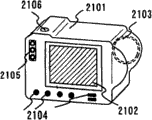
Fig. 5 B represents digital camera, is made up of body 2101, display unit 2102, image receiving unit 2103, operation keys 2104, external cabling mouth 2105, shutter 2106 etc.Light-emitting device by manufacturing of the present invention can be applicable on this display unit 2102.
Fig. 5 C represents notebook, is made up of body 2201, casing 2202, display unit 2203, keyboard 2204, external cabling mouth 2205, sensing mouse 2206 etc.Light-emitting device by manufacturing of the present invention may be used on this display unit 2203.
Fig. 5 D represents removable computer, is made up of body 2301, display unit 2302, switch 2303, operation keys 2304, infrared mouth 2305 etc.Light-emitting device by manufacturing of the present invention may be used on this display unit 2302.
Fig. 5 E represents to be equipped with the portable image playing device (specifically, DVD display) of recording medium.This device is made up of body 2401, casing 2402, display unit A2403, display unit B2404, recording medium (DVD and so on) reading unit 2405, operation keys 2406, loudspeaker unit 2407 etc.The main displays image information of display unit A2403, and the main videotex information of display unit B2404.Light-emitting device by manufacturing of the present invention may be used on display unit A2403 and the B2404.This image playing device that has been equipped with recording medium also comprises the family game machine.
Fig. 5 F represents goggles formula display (helmet-mounted display), is made up of body 2501, display unit 2502 and arm unit 2503.Light-emitting device by manufacturing of the present invention may be used on the display unit 2502.
Fig. 5 G represents video camera, is made up of body 2601, display unit 2602, casing 2603, external interface 2604, remote control receiving element 2605, image receiving unit 2606, battery 2607, audio frequency input unit 2608, operation keys 2609, eyepiece part 2610 etc.Light-emitting device by manufacturing of the present invention may be used on the display unit 2602.
Fig. 5 H represents mobile phone, is made up of body 2701, casing 2702, display unit 2703, audio frequency input unit 2704, audio output unit 2705, operation keys 2706, external interface 2707, antenna 2708 etc.Light-emitting device by manufacturing of the present invention may be used on the display unit 2703.If display unit 2703 shows the black background wrongly written or mispronounced character, then this mobile phone power consumption is less.
If improved in the future the brightness that organic material sends light, before or after then this light-emitting device can be used in the projector, output light transmission lens of being loaded with image information and so on are amplified and this light is throwed away.
At present, these electronic equipments show the information, particularly animation information that sends by electronic communication line such as the Internet or CATV (cable TV) etc. just more and more.In view of organic material has very fast response speed,, this light-emitting device shows so being applicable to animation.
In this light-emitting device, the luminous component consumed power, therefore preferred to require the mode display message of less luminous component.When this light-emitting device is used in the portable information terminal display unit, especially in the time of in the device of the main display text information of this class of mobile phone or audio playing apparatus, preferred following mode drives such device, even luminous component does not form background, and luminous component forms Word message.
As mentioned above, the range of application of the light-emitting device that employing the present invention makes is so extensive, so that it may be used on the electronic equipment in any field.The electronic equipment of this embodiment pattern 4 can be finished by the light-emitting device that adopts embodiment pattern 1~3 to be shaped.
By implementing the present invention, not only can prevent to make the material of light-emitting component degeneration from outside invading like this such as moisture or oxygen etc., and, can solve in employing and contain the problem that causes the metallic material corrosion of light-emitting component in the situation of film of fluororesin because of fluorine element.
Claims (22)
1. a light-emitting device comprises:
Has light-emitting component at first electrode that forms on the substrate, the electroluminescent film that on described first electrode, forms and second electrode that on described electroluminescent film, forms;
The inorganic insulating membrane that on described second electrode, forms;
The film that contains fluororesin that on described inorganic insulating membrane, forms; And
Be positioned at the seal substrate on the described film that contains fluororesin, between described seal substrate and the described film that contains fluororesin, have the space,
Wherein, by described seal substrate being pasted described substrate, make described light-emitting component, described inorganic insulating membrane and the described film that contains fluororesin sealed with encapsulant.
2. according to the light-emitting device of claim 1, the wherein said film that contains fluororesin is to be selected from polytetrafluoroethylene, tetrafluoraoethylene-hexafluoropropylene copolymer (tetrafluoroethylene-hexafluoropropylene copolymer), polychlorotrifluoroethylene (is abbreviated as PCTFE, Polychlorotrifluoroethylene), tetrafluoroethylene-ethylene copolymer (tetrafluoroethylene-ethylene copolymer), polyvinyl fluoride (is abbreviated as PVF, Poly vinyl fluoride), a kind of polymer in the Kynoar (being abbreviated as PVDF, Polyvinylidene Fluoride).
3. according to the light-emitting device of claim 1, wherein said inorganic insulating membrane is by silicon nitride, oxidized silicon nitride, aluminium nitride, a kind of in the nitriding and oxidizing aluminium and forming.
4. a light-emitting device comprises:
Has light-emitting component at first electrode that forms on the substrate, the electroluminescent film that on described first electrode, forms and second electrode that on described electroluminescent film, forms;
The inorganic insulating membrane that on described second electrode, forms;
The organic insulating film that on described inorganic insulating membrane, forms;
The film that contains fluororesin that on described organic insulating film, forms; And
Be positioned at the seal substrate on the described film that contains fluororesin, between described seal substrate and the described film that contains fluororesin, have the space,
Wherein, by described seal substrate being pasted described substrate, make described light-emitting component, described inorganic insulating membrane, described organic insulating film and the described film that contains fluororesin sealed with encapsulant.
5. according to the light-emitting device of claim 4, the wherein said film that contains fluororesin is to be selected from polytetrafluoroethylene, tetrafluoraoethylene-hexafluoropropylene copolymer (tetrafluoroethylene-hexafluoropropylene copolymer), polychlorotrifluoroethylene (is abbreviated as PCTFE, Polychlorotrifluoroethylene), tetrafluoroethylene-ethylene copolymer (tetrafluoroethylene-ethylene copolymer), polyvinyl fluoride (is abbreviated as PVF, Poly vinyl fluoride), a kind of polymer in the Kynoar (being abbreviated as PVDF, Polyvinylidene Fluoride).
6. according to the light-emitting device of claim 4, wherein said inorganic insulating membrane is by silicon nitride, oxidized silicon nitride, aluminium nitride, a kind of in the nitriding and oxidizing aluminium and forming.
7. according to the light-emitting device of claim 4, wherein said organic insulating film is by acrylic acid, polyamide, a kind of in the polyimides and forming.
8. a light-emitting device comprises:
Has light-emitting component at first electrode that forms on the substrate, the electroluminescent film that on described first electrode, forms and second electrode that on described electroluminescent film, forms;
First inorganic insulating membrane that on described second electrode, forms;
The organic insulating film that on described first inorganic insulating membrane, forms;
Second inorganic insulating membrane that on described organic insulating film, forms;
The film that contains fluororesin that on described second inorganic insulating membrane, forms; And
Be positioned at the seal substrate on the described film that contains fluororesin, between described seal substrate and the described film that contains fluororesin, have the space,
Wherein, by described seal substrate being pasted described substrate, make described light-emitting component, described first inorganic insulating membrane, described organic insulating film, described second inorganic insulating membrane and the described film that contains fluororesin sealed with encapsulant.
9. light-emitting device according to Claim 8, the wherein said film that contains fluororesin is to be selected from polytetrafluoroethylene, tetrafluoraoethylene-hexafluoropropylene copolymer (tetrafluoroethylene-hexafluoropropylene copolymer), polychlorotrifluoroethylene (is abbreviated as PCTFE, Polychlorotrifluoroethylene), tetrafluoroethylene-ethylene copolymer (tetrafluoroethylene-ethylene copolymer), polyvinyl fluoride (is abbreviated as PVF, Poly vinyl fluoride), a kind of polymer in the Kynoar (being abbreviated as PVDF, Polyvinylidene Fluoride).
10. light-emitting device according to Claim 8, wherein said first inorganic insulating membrane and second inorganic insulating membrane be respectively by silicon nitride, oxidized silicon nitride, aluminium nitride, a kind of in the nitriding and oxidizing aluminium and forming.
11. light-emitting device according to Claim 8, wherein said organic insulating film be by acrylic acid, polyamide, a kind of in the polyimides and forming.
12. a light-emitting device comprises:
Light-emitting component with first electrode, the electroluminescent film that on described first electrode, forms that is electrically connected via the TFT that forms on dielectric film and the substrate and second electrode that on described electroluminescent film, forms;
The inorganic insulating membrane that on described second electrode, forms;
The film that contains fluororesin that on described inorganic insulating membrane, forms; And
Be positioned at the seal substrate on the described film that contains fluororesin, between described seal substrate and the described film that contains fluororesin, have the space,
Wherein, by described seal substrate being pasted described substrate, make described light-emitting component, described inorganic insulating membrane and the described film that contains fluororesin sealed with encapsulant.
13. light-emitting device according to claim 12, the wherein said film that contains fluororesin is to be selected from polytetrafluoroethylene, tetrafluoraoethylene-hexafluoropropylene copolymer (tetrafluoroethylene-hexafluoropropylene copolymer), polychlorotrifluoroethylene (is abbreviated as PCTFE, Polychlorotrifluoroethylene), tetrafluoroethylene-ethylene copolymer (tetrafluoroethylene-ethylene copolymer), polyvinyl fluoride (is abbreviated as PVF, Poly vinyl fluoride), a kind of polymer in the Kynoar (being abbreviated as PVDF, Polyvinylidene Fluoride).
14. according to the light-emitting device of claim 12, wherein said inorganic insulating membrane is by silicon nitride, oxidized silicon nitride, aluminium nitride, a kind of in the nitriding and oxidizing aluminium and forming.
15. a light-emitting device comprises:
Light-emitting component with first electrode, the electroluminescent film that on described first electrode, forms that is electrically connected via the TFT that forms on dielectric film and the substrate and second electrode that on described electroluminescent film, forms;
The inorganic insulating membrane that on described second electrode, forms;
The organic insulating film that on described inorganic insulating membrane, forms;
The film that contains fluororesin that on described organic insulating film, forms; And
Be positioned at the seal substrate on the described film that contains fluororesin, between described seal substrate and the described film that contains fluororesin, have the space,
Wherein, by described seal substrate being pasted described substrate, make described light-emitting component, described inorganic insulating membrane, described organic insulating film and the described film that contains fluororesin sealed with encapsulant.
16. light-emitting device according to claim 15, the wherein said film that contains fluororesin is to be selected from polytetrafluoroethylene, tetrafluoraoethylene-hexafluoropropylene copolymer (tetrafluoroethylene-hexafluoropropylene copolymer), polychlorotrifluoroethylene (is abbreviated as PCTFE, Polychlorotrifluoroethylene), tetrafluoroethylene-ethylene copolymer (tetrafluoroethylene-ethylene copolymer), polyvinyl fluoride (is abbreviated as PVF, Poly vinyl fluoride), a kind of polymer in the Kynoar (being abbreviated as PVDF, Polyvinylidene Fluoride).
17. according to the light-emitting device of claim 15, wherein said inorganic insulating membrane is by silicon nitride, oxidized silicon nitride, aluminium nitride, a kind of in the nitriding and oxidizing aluminium and forming.
18. according to the light-emitting device of claim 15, wherein said organic insulating film is by acrylic acid, polyamide, a kind of in the polyimides and forming.
19. a light-emitting device comprises:
Light-emitting component with first electrode, the electroluminescent film that on described first electrode, forms that is electrically connected via the TFT that forms on dielectric film and the substrate and second electrode that on described electroluminescent film, forms;
First inorganic insulating membrane that on described second electrode, forms;
The organic insulating film that on described first inorganic insulating membrane, forms;
Second inorganic insulating membrane that on described organic insulating film, forms;
The film that contains fluororesin that on described second inorganic insulating membrane, forms; And
Be positioned at the seal substrate on the described film that contains fluororesin, between described seal substrate and the described film that contains fluororesin, have the space,
Wherein, by described seal substrate being pasted described substrate, make described light-emitting component, described first inorganic insulating membrane, described organic insulating film, described second inorganic insulating membrane and the described film that contains fluororesin sealed with encapsulant.
20. light-emitting device according to claim 19, the wherein said film that contains fluororesin is to be selected from polytetrafluoroethylene, tetrafluoraoethylene-hexafluoropropylene copolymer (tetrafluoroethylene-hexafluoropropylene copolymer), polychlorotrifluoroethylene (is abbreviated as PCTFE, Polychlorotrifluoroethylene), tetrafluoroethylene-ethylene copolymer (tetrafluoroethylene-ethylene copolymer), polyvinyl fluoride (is abbreviated as PVF, Poly vinyl fluoride), a kind of polymer in the Kynoar (being abbreviated as PVDF, Polyvinylidene Fluoride).
21. according to the light-emitting device of claim 19, wherein said first inorganic insulating membrane and second inorganic insulating membrane be respectively by silicon nitride, oxidized silicon nitride, aluminium nitride, a kind of in the nitriding and oxidizing aluminium and forming.
22. according to the light-emitting device of claim 19, wherein said organic insulating film is by acrylic acid, polyamide, a kind of in the polyimides and forming.
Applications Claiming Priority (3)
| Application Number | Priority Date | Filing Date | Title |
|---|---|---|---|
| JP276382/02 | 2002-09-20 | ||
| JP276382/2002 | 2002-09-20 | ||
| JP2002276382A JP2004119016A (en) | 2002-09-20 | 2002-09-20 | Light emitting device |
Publications (2)
| Publication Number | Publication Date |
|---|---|
| CN1492723A CN1492723A (en) | 2004-04-28 |
| CN100576595C true CN100576595C (en) | 2009-12-30 |
Family
ID=31944624
Family Applications (1)
| Application Number | Title | Priority Date | Filing Date |
|---|---|---|---|
| CN03158666A Expired - Fee Related CN100576595C (en) | 2002-09-20 | 2003-09-19 | Light-emitting device |
Country Status (6)
| Country | Link |
|---|---|
| US (1) | US7268487B2 (en) |
| EP (1) | EP1401032A3 (en) |
| JP (1) | JP2004119016A (en) |
| KR (1) | KR20040025834A (en) |
| CN (1) | CN100576595C (en) |
| TW (1) | TWI369917B (en) |
Families Citing this family (20)
| Publication number | Priority date | Publication date | Assignee | Title |
|---|---|---|---|---|
| JP2004119015A (en) * | 2002-09-20 | 2004-04-15 | Semiconductor Energy Lab Co Ltd | Light emitting device and its manufacturing method |
| US20040099926A1 (en) * | 2002-11-22 | 2004-05-27 | Semiconductor Energy Laboratory Co., Ltd. | Semiconductor device, display device, and light-emitting device, and methods of manufacturing the same |
| US7652359B2 (en) * | 2002-12-27 | 2010-01-26 | Semiconductor Energy Laboratory Co., Ltd. | Article having display device |
| JP4785415B2 (en) * | 2004-05-14 | 2011-10-05 | 株式会社半導体エネルギー研究所 | Method for manufacturing electroluminescence display device |
| EP1655790B1 (en) * | 2004-10-21 | 2010-08-04 | LG Display Co., Ltd. | Organic electroluminescent device and method of manufacturing the same |
| WO2007055299A1 (en) * | 2005-11-09 | 2007-05-18 | Semiconductor Energy Laboratory Co., Ltd. | Semiconductor device and manufacturing method thereof |
| EP2031036B1 (en) * | 2007-08-31 | 2012-06-27 | Semiconductor Energy Laboratory Co., Ltd. | Light-emitting element, light-emitting device, and electronic appliance |
| CN101971235B (en) * | 2008-03-04 | 2013-09-18 | 夏普株式会社 | Display device substrate, method for manufacturing the same, display device, method for forming multi-layer wiring, and multi-layer wiring substrate |
| TWI388056B (en) * | 2008-12-05 | 2013-03-01 | Chunghwa Picture Tubes Ltd | Organic electro-luminescence device |
| US9000442B2 (en) * | 2010-01-20 | 2015-04-07 | Semiconductor Energy Laboratory Co., Ltd. | Light-emitting device, flexible light-emitting device, electronic device, and method for manufacturing light-emitting device and flexible-light emitting device |
| TWI589042B (en) | 2010-01-20 | 2017-06-21 | 半導體能源研究所股份有限公司 | Light-emitting device, flexible light-emitting device, electronic device, lighting apparatus, and method of manufacturing light-emitting device and flexible-light emitting device |
| KR101033963B1 (en) * | 2010-09-24 | 2011-05-11 | 엘지이노텍 주식회사 | Light emitting device array module and method for forming protective film of the same |
| KR20120109081A (en) * | 2011-03-24 | 2012-10-08 | 삼성디스플레이 주식회사 | Organic light emitting diode display |
| CN102856503A (en) * | 2011-06-28 | 2013-01-02 | 海洋王照明科技股份有限公司 | Organic electroluminescent device and preparation method thereof |
| CN103035663B (en) * | 2011-10-04 | 2016-08-10 | 乐金显示有限公司 | Display device |
| KR101643012B1 (en) * | 2011-10-04 | 2016-07-28 | 엘지디스플레이 주식회사 | Display device |
| KR102000709B1 (en) * | 2012-08-31 | 2019-09-30 | 삼성디스플레이 주식회사 | Manufacturing method of a display panel |
| CN105493627A (en) | 2013-08-28 | 2016-04-13 | 夏普株式会社 | Electroluminescent device and method for manufacturing same |
| KR102539668B1 (en) * | 2016-06-30 | 2023-06-02 | 엘지이노텍 주식회사 | Semiconductor device, display panel, display device and communication device having the same |
| KR102421576B1 (en) * | 2017-03-10 | 2022-07-18 | 삼성디스플레이 주식회사 | Organic light-emitting apparatus and the method for manufacturing of the organic light-emitting display apparatus |
Family Cites Families (56)
| Publication number | Priority date | Publication date | Assignee | Title |
|---|---|---|---|---|
| JPS5435780B2 (en) * | 1974-07-23 | 1979-11-05 | ||
| US4417174A (en) * | 1980-10-03 | 1983-11-22 | Alps Electric Co., Ltd. | Electroluminescent cell and method of producing the same |
| JPS60115944A (en) | 1983-11-29 | 1985-06-22 | Asahi Chem Ind Co Ltd | Electrophotographic sensitive body |
| US4580818A (en) * | 1984-10-25 | 1986-04-08 | Lyng William E | Locker latching assembly |
| JPH0265895U (en) * | 1988-11-07 | 1990-05-17 | ||
| JPH03153859A (en) | 1989-11-08 | 1991-07-01 | Sekisui Chem Co Ltd | Surface-modified plastic |
| US5188876A (en) * | 1990-04-12 | 1993-02-23 | Armstrong World Industries, Inc. | Surface covering with inorganic wear layer |
| US5427858A (en) * | 1990-11-30 | 1995-06-27 | Idemitsu Kosan Company Limited | Organic electroluminescence device with a fluorine polymer layer |
| JP2597047B2 (en) | 1990-12-28 | 1997-04-02 | 出光興産株式会社 | Organic electroluminescent device |
| JP2813495B2 (en) | 1991-07-26 | 1998-10-22 | 出光興産株式会社 | Organic EL element sealing method |
| JP2813499B2 (en) | 1991-09-30 | 1998-10-22 | 出光興産株式会社 | Organic EL device |
| JPH05101884A (en) | 1991-10-11 | 1993-04-23 | Idemitsu Kosan Co Ltd | Sealing method and patterning method of organic electroluminescent element |
| JPH06306591A (en) | 1993-04-28 | 1994-11-01 | Sekisui Chem Co Ltd | Production of water-repellent hard-coated coating film |
| US5834327A (en) * | 1995-03-18 | 1998-11-10 | Semiconductor Energy Laboratory Co., Ltd. | Method for producing display device |
| US6027958A (en) * | 1996-07-11 | 2000-02-22 | Kopin Corporation | Transferred flexible integrated circuit |
| DE69739368D1 (en) * | 1996-08-27 | 2009-05-28 | Seiko Epson Corp | Separation method and method for transferring a thin film device |
| JP3809681B2 (en) | 1996-08-27 | 2006-08-16 | セイコーエプソン株式会社 | Peeling method |
| EP0946993B8 (en) * | 1996-09-04 | 2007-09-12 | Cambridge Display Technology Limited | Electrode deposition for organic light-emitting devices |
| US5952778A (en) * | 1997-03-18 | 1999-09-14 | International Business Machines Corporation | Encapsulated organic light emitting device |
| JPH10321374A (en) | 1997-05-20 | 1998-12-04 | Tdk Corp | Organic el(electroluminescent)element |
| US6198220B1 (en) * | 1997-07-11 | 2001-03-06 | Emagin Corporation | Sealing structure for organic light emitting devices |
| US6800378B2 (en) * | 1998-02-19 | 2004-10-05 | 3M Innovative Properties Company | Antireflection films for use with displays |
| TW420965B (en) * | 1998-07-14 | 2001-02-01 | Matsushita Electric Ind Co Ltd | Dispersion-type electroluminescence element |
| US6198092B1 (en) * | 1998-08-19 | 2001-03-06 | The Trustees Of Princeton University | Stacked organic photosensitive optoelectronic devices with an electrically parallel configuration |
| US6274887B1 (en) * | 1998-11-02 | 2001-08-14 | Semiconductor Energy Laboratory Co., Ltd. | Semiconductor device and manufacturing method therefor |
| US6652938B1 (en) * | 1998-11-09 | 2003-11-25 | Kaneka Corporation | Media transport belt |
| CN1348609A (en) * | 1999-04-28 | 2002-05-08 | E·I·内穆尔杜邦公司 | Flexible organic electronic device with improved resistance to oxygen and moisture degradation |
| TWI232595B (en) * | 1999-06-04 | 2005-05-11 | Semiconductor Energy Lab | Electroluminescence display device and electronic device |
| TW522453B (en) * | 1999-09-17 | 2003-03-01 | Semiconductor Energy Lab | Display device |
| JP3942770B2 (en) * | 1999-09-22 | 2007-07-11 | 株式会社半導体エネルギー研究所 | EL display device and electronic device |
| JP2001267578A (en) * | 2000-03-17 | 2001-09-28 | Sony Corp | Thin-film semiconductor device, and method for manufacturing the same |
| US6936485B2 (en) * | 2000-03-27 | 2005-08-30 | Semiconductor Energy Laboratory Co., Ltd. | Method of manufacturing a light emitting device |
| US7525165B2 (en) * | 2000-04-17 | 2009-04-28 | Semiconductor Energy Laboratory Co., Ltd. | Light emitting device and manufacturing method thereof |
| US6664732B2 (en) * | 2000-10-26 | 2003-12-16 | Semiconductor Energy Laboratory Co., Ltd. | Light emitting device and manufacturing method thereof |
| TW522577B (en) * | 2000-11-10 | 2003-03-01 | Semiconductor Energy Lab | Light emitting device |
| US6583440B2 (en) * | 2000-11-30 | 2003-06-24 | Seiko Epson Corporation | Soi substrate, element substrate, semiconductor device, electro-optical apparatus, electronic equipment, method of manufacturing the soi substrate, method of manufacturing the element substrate, and method of manufacturing the electro-optical apparatus |
| US6717181B2 (en) * | 2001-02-22 | 2004-04-06 | Semiconductor Energy Laboratory Co., Ltd. | Luminescent device having thin film transistor |
| JP4147008B2 (en) * | 2001-03-05 | 2008-09-10 | 株式会社日立製作所 | Film used for organic EL device and organic EL device |
| US20020153833A1 (en) * | 2001-04-18 | 2002-10-24 | Alvin Wu | Full-color electroluminescent lamp and manufacturing method for same |
| US7211828B2 (en) * | 2001-06-20 | 2007-05-01 | Semiconductor Energy Laboratory Co., Ltd. | Light emitting device and electronic apparatus |
| JP2003084123A (en) * | 2001-06-29 | 2003-03-19 | Seiko Epson Corp | Color filter substrate, method for manufacturing color filter substrate, liquid crystal display device, electrooptical device, method for manufacturing electrooptical device and electronic apparatus |
| TW564471B (en) * | 2001-07-16 | 2003-12-01 | Semiconductor Energy Lab | Semiconductor device and peeling off method and method of manufacturing semiconductor device |
| KR100413450B1 (en) * | 2001-07-20 | 2003-12-31 | 엘지전자 주식회사 | protecting film structure for display device |
| TW490868B (en) * | 2001-08-10 | 2002-06-11 | Ritdisplay Corp | Method for forming a waterproof layer of organic light emitting device |
| TW554398B (en) * | 2001-08-10 | 2003-09-21 | Semiconductor Energy Lab | Method of peeling off and method of manufacturing semiconductor device |
| KR100393229B1 (en) * | 2001-08-11 | 2003-07-31 | 삼성전자주식회사 | Method of manufacturing non-volatile memory device including self-aligned gate structure and device by the same |
| US20030048074A1 (en) * | 2001-09-12 | 2003-03-13 | Jui-Ming Ni | Method for packaging organic electroluminescent components with polymer passivation layer and structure thereof |
| US7071613B2 (en) * | 2001-10-10 | 2006-07-04 | Lg.Philips Lcd Co., Ltd. | Organic electroluminescent device |
| US6926572B2 (en) * | 2002-01-25 | 2005-08-09 | Electronics And Telecommunications Research Institute | Flat panel display device and method of forming passivation film in the flat panel display device |
| US7164155B2 (en) * | 2002-05-15 | 2007-01-16 | Semiconductor Energy Laboratory Co., Ltd. | Light emitting device |
| JP4052631B2 (en) * | 2002-05-17 | 2008-02-27 | 株式会社東芝 | Active matrix display device |
| US6792333B2 (en) * | 2002-06-04 | 2004-09-14 | Semiconductor Energy Laboratory Co., Ltd. | Product management method, program for performing product management, and storage medium having recorded the program therein |
| JP2004119015A (en) * | 2002-09-20 | 2004-04-15 | Semiconductor Energy Lab Co Ltd | Light emitting device and its manufacturing method |
| US20040099926A1 (en) * | 2002-11-22 | 2004-05-27 | Semiconductor Energy Laboratory Co., Ltd. | Semiconductor device, display device, and light-emitting device, and methods of manufacturing the same |
| US6936761B2 (en) * | 2003-03-29 | 2005-08-30 | Nanosolar, Inc. | Transparent electrode, optoelectronic apparatus and devices |
| US6919681B2 (en) * | 2003-04-30 | 2005-07-19 | Eastman Kodak Company | Color OLED display with improved power efficiency |
-
2002
- 2002-09-20 JP JP2002276382A patent/JP2004119016A/en not_active Withdrawn
-
2003
- 2003-09-03 TW TW092124359A patent/TWI369917B/en not_active IP Right Cessation
- 2003-09-16 US US10/662,357 patent/US7268487B2/en not_active Expired - Fee Related
- 2003-09-18 KR KR1020030064762A patent/KR20040025834A/en active Search and Examination
- 2003-09-19 EP EP03021328A patent/EP1401032A3/en not_active Withdrawn
- 2003-09-19 CN CN03158666A patent/CN100576595C/en not_active Expired - Fee Related
Also Published As
| Publication number | Publication date |
|---|---|
| TWI369917B (en) | 2012-08-01 |
| JP2004119016A (en) | 2004-04-15 |
| US20040056589A1 (en) | 2004-03-25 |
| US7268487B2 (en) | 2007-09-11 |
| CN1492723A (en) | 2004-04-28 |
| KR20040025834A (en) | 2004-03-26 |
| TW200410594A (en) | 2004-06-16 |
| EP1401032A3 (en) | 2007-06-13 |
| EP1401032A2 (en) | 2004-03-24 |
Similar Documents
| Publication | Publication Date | Title |
|---|---|---|
| CN100576595C (en) | Light-emitting device | |
| US9263476B2 (en) | Display device and method for fabricating the same | |
| US7128632B2 (en) | Method for manufacturing light-emitting device | |
| JP4240276B2 (en) | Light emitting device | |
| US6882102B2 (en) | Light emitting device and manufacturing method thereof | |
| US7220988B2 (en) | Luminescent device and process of manufacturing the same | |
| JP2018180549A (en) | El display device | |
| JP2019036556A (en) | Light-emitting device | |
| US20050231123A1 (en) | Semiconductor device | |
| JP2004103337A (en) | Light-emitting device and its manufacturing method | |
| JP2003092191A (en) | Luminescent device and method for manufacturing the same | |
| CN100557850C (en) | Light-emitting device and preparation method thereof | |
| JP2001195016A (en) | Electronic device | |
| JP4215750B2 (en) | Method for manufacturing light emitting device | |
| JP5052577B2 (en) | EL display device | |
| JP2012069534A (en) | Light-emitting device | |
| JP2012109257A (en) | Light-emitting device | |
| JP2010238678A (en) | Method of manufacturing light emitting device, and light emitting device | |
| JP5520995B2 (en) | EL display device | |
| JP2014044958A (en) | Light-emitting device |
Legal Events
| Date | Code | Title | Description |
|---|---|---|---|
| C06 | Publication | ||
| PB01 | Publication | ||
| C10 | Entry into substantive examination | ||
| SE01 | Entry into force of request for substantive examination | ||
| C14 | Grant of patent or utility model | ||
| GR01 | Patent grant | ||
| CF01 | Termination of patent right due to non-payment of annual fee |
Granted publication date: 20091230 Termination date: 20200919 |
|
| CF01 | Termination of patent right due to non-payment of annual fee |