Embodiment
At first with respect to Fig. 1-6 common flash memory system is described.In this system, can implement various aspects of the present invention.The host computer system 1 of Fig. 1 stores data in the flash memory 2 into and from retrieve data wherein.Although flash memory can be embedded in the main frame, storer 2 is illustrated as card than common form, its mating part 3 and 4 by machinery and electrical cnnector is connected to main frame removedly.Have at present many different commercially available flash memory cards, example is compact flash memory (CF), multimedia card (MMC), secure digital (SD), small-sized SD, memory stick, smart media and TransFlash card.Although each in these cards all has machinery and/or electric interfaces according to the uniqueness of its standard convention, the flash memory system that comprises in each is similar.These cards can be buied from the assignee SanDisk company of the application's case.SanDisk also provides the line of the flash drive take Cruzer as trade mark, and it is the hand-held accumulator system of little encapsulation, and described system has the USB plug that is connected with main frame for by USB (universal serial bus) (USB) socket that inserts main frame.In these memory cards and the flash drive each all comprises the controller that connects and control the operation of flash memory in it with main frame Jie.
Use the host computer system of these memory cards and flash drive to have many and of all kinds.They comprise personal computer (PC), on knee and other portable computer, cellular phone, personal digital assistant (PDA), Digital Still Camera, digital movie camera and portable audio player.Main frame comprises the built-in socket for the memory card of one or more types or flash drive usually, but some of them need to insert the adapter of memory card.Accumulator system contains Memory Controller and the driver of himself usually, but the system that also has some that storer is only arranged, it is alternatively controlled by the performed software of the main frame that is connected with storer.In containing some accumulator systems of controller, especially be embedded in those accumulator systems in the main frame, storer, controller and driver often are formed on the single integrated circuit chip.
The host computer system 1 of Fig. 1 can be considered in the scope of paying close attention to storer 2 and has two major parts, and it is constituted by circuit and software.They are application program part 5 and the driver part 6 that is situated between and connects with storer 2.In personal computer for example, application program part 5 can comprise the processor of operation word processing, figure, control or other popular application software.Mainly be exclusively used in the host computer system of carrying out the simple function set at camera, cellular phone or other, application program part 5 comprises the operation camera with shooting and storage picture, the software of operation cellular phone to make a phone call and to answer the call etc.
The accumulator system 2 of Fig. 1 comprises flash memory 7 and circuit 8, circuit 8 and with link that connecing is situated between with the main frame that is used for transmitting back and forth data connects, and go back control store 7.Controller 8 is changed between the physical address of the logical address of the data that main frame 1 uses and storer 7 at data programing and during read usually.
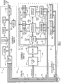
Referring to Fig. 2, its description can be used as the circuit of typical flash memory system of the nonvolatile memory 2 of Fig. 1.System controller is implemented on the single integrated circuit chip 11 usually, and it is connected in parallel by system bus 13 and one or more integrated circuit memory chips, shows single sort memory chip 15 among Fig. 2.Illustrated specific bus 13 comprises be used to the independent one group of conductor 17 that carries data, the one group of conductor 19 that is used for storage address and the one group of conductor 21 that is used for control and status signal.Perhaps, single one group of conductor can be between this three functions the time share.In addition, can adopt other configuration of system bus, the ring bus of for example describing in the 10/915th, No. 039 U.S. patent application case that is entitled as " Ring Bus Structure and It ' sUse in Flash Memory Systems " of application on August 9th, 2004.
Typical controller chip 11 has the internal bus 23 of himself, and internal bus 23 is situated between with system bus 13 by interface circuit 25 and connects.The major function part that is typically connected to bus is processor 27 (for example microprocessor or microcontroller), contain the ROM (read-only memory) (ROM) 29 of the code that is useful on initialization (" guiding ") system, be mainly used in random access memory (RAM) 31 that the data that transmit between storer and the main frame are cushioned, and the circuit 33 that the error-correcting code (ECC) of the data that are used for passing through the controller between storer and the main frame is calculated and checked.Controller bus 23 is situated between with host computer system by circuit 35 and connects, and under the system of Fig. 2 was included in situation in the memory card, institute gives an account of and connects was that the external connector 37 as the part of connector 4 by blocking is finished.Clock 39 is connected with each other assembly of controller 11 and by its use.
Memory chip 15 and any chip that other is connected with system bus 13 contain the memory cell array that is organized into a plurality of subarrays or plane usually, two this planes 41 and 43 are described for brevity, but the more planes of alternative use, for example four or eight this planes.Perhaps, can be not the memory cell array of chip 15 be divided into the plane.Yet when so dividing, each plane has the arrange control circuit that can operate independently of one another 45 and 47 of himself. Circuit 45 and 47 address portions 19 from system bus 13 receive its separately address of memory cell array, and it is decoded specific one or more in the bit line 49 and 51 separately to be carried out addressing.Come addressed word line 53 in response to the address that receives at address bus 19 by line control circuit 55.Source voltage control circuit 57 is connected with the plane of being connected also with separately, as p trap voltage control circuit 61 and 63.If memory chip 15 has the single memory cell array, and if have two or more this chips in the system, can be similar to so the array that the interior plane of above-mentioned many planar chip or subarray operate each chip.
Data communication device is crossed the separately data input/output circuit 65 that is connected with the data division 17 of system bus 13 and 67 and transmit and send out plane 41 and 43. Circuit 65 and 67 is used for by be connected to the line 69 and 71 on plane via arrange control circuit 45 and 47 separately, programs data in the memory cell and from its memory cell reading out data on plane separately.
Although the operation of controller 11 control store chips 15 comes programming data, reading out data, wipes and look after various housekeeping events, each memory chip also contains certain control circuit, and its order of carrying out self-controller 11 is to carry out these functions.Interface circuit 73 is connected to control and the state part 21 of system bus 13.The in the future order of self-controller is provided to state machine 75, and state machine 75 then provides the specific control of other circuit in order to carry out these orders.Control line 77-81 connect state machine 75 and described other circuit, as shown in Figure 2.Status information from state machine 75 is sent to interface 73 by line 83, to be used for being transferred to controller 11 by bus portion 21.
Memory cell array 41 and 43 enable nand gate are preferred at present, but also alternative use other structure of NOR for example.Can be with reference to the 5th, 570 as the example of the NAND flash memory of the part of accumulator system and operation thereof, 315,5,774,397,6,046,935,6,373,746,6,456,528,6,522,580,6,771,536 and 6,781, No. 877 United States Patent (USP)s and No. 2003/0147278 U.S. Patent Application Publication case.
Circuit diagram by Fig. 3 illustrates exemplary NAND array, and it is the part of memory cell array 41 of the accumulator system of Fig. 2.A large amount of global bit line are provided, but for the purpose of explaining for the sake of simplicity, in Fig. 3, only show four this type of line 91-94.Many memory cell strings 97-104 that are connected in series are connected between one of these bit lines and the reference potential.Use memory cell strings 99 as representative, a plurality of charge storage memory cell 107-110 are connected in series with selecting transistor 111 and 112 at arbitrary end place of string.When making the selection transistor conduction of a string, described series winding is connected between its bit line and the reference potential.Then a memory cell in the described string is carried out one-time programming or read.
Individually extend on the charge storage cell of a memory cell during the word line 115-118 of Fig. 3 is whenever a string in many memory cell strings, and the transistorized state of selection at each end place of grid 119 and 120 control strings.Make the memory cell strings of sharing common word line and control gate polar curve 115-120 form the block of memory cells 123 that jointly to wipe.This element block contains the unit of minimal amount that can disposable physical erase.Once to programming along the row of memory cells of one of word line 115-118.Usually, with predesigned order the row of NAND array being programmed, is the row beginning with the word line 118 of the end of the most close string that is connected to ground connection or another common potential in the case.Then to programming along the column of memory cells of word line 117, so in whole block 123, carry out.At last to programming along the row of word line 115.
The second block 125 is similarly, its memory cell be series-connected to the first block 123 in the identical global bit line that connects of string, but have different one group of word line and control gate polar curve.By line control circuit 55 word line and control gate polar curve are driven into its suitable operating voltage.If have an above plane or subarray in the system, the plane 1 and 2 of Fig. 2 for example, so a kind of memory construction is used the common word line of extending between it.Alternatively can there be two above planes or the subarray of sharing common word line.In other memory construction, drive separately the word line of indivedual planes or subarray.
Described in some NAND patents and above-cited open application case, but the operational store system with the detectable charge level more than two of storage in each charge storage cell or zone, and then in each above data bit of storage.The charge storage cell of memory cell is the conductive floating gate utmost point the most normally, but alternatively can be non-conductive dielectric charge material for trapping, described in No. 2003/0109093 U.S. Patent Application Publication case.
Fig. 4 conceptual illustration is as the tissue of the flash memory cell array 7 (Fig. 1) of the example in hereinafter further describing.Four planes or the subarray 131-134 of memory cell can be on single integrated memory unit chips, on (two planes on each chip) on two chips or on four independent chips.Concrete layout is inessential concerning discussion hereinafter.Certainly, in system, can there be the plane of other number, for example 1,2,8,16 or more.The plane individually is divided into the block of memory cells of showing with rectangle among Fig. 4, for example is arranged in the separately block 137,138,139 and 140 of plane 131-134.Can there be dozens of or hundreds of blocks in each plane.As mentioned above, block of memory cells is the unit of wiping, and is the minimum number destination memory location that physically can jointly wipe.Yet for the concurrency that increases, come the operation block take larger first block as unit.To link together in logic to form first block from a block on each plane.Show that four block 137-140 form a first block 141.All unit in unit's block are wiped usually jointly.The block that is used to form first block need not to be limited to its separately identical relative position in the plane, as shown in the second yuan of block 143 that is comprised of block 145-148.Although preferably extend first block on all planes obtaining high system performance, can be in Different Plane the ability of dynamic formation with any or whole first block among one, two or three blocks come the operational store system.This size that allows first block more closely with the one-time programming operation in the data volume coupling that can be used for storing.
In order to operate purpose, again individual block is divided into page of memory cells, such as Fig. 5 explanation.For example the memory cell of each respectively is divided into eight page or leaf P0-P7 among the block 131-134.Perhaps, can there be 16,32 or multi-memory page of cells more in each block.Page or leaf is data programing and the unit that reads, the minimum data amount that contains one-time programming or read in block.In the enable nand gate of Fig. 3, page or leaf is formed by the memory cell of word line in block.Yet in order to increase accumulator system operation concurrency, the described page or leaf in two or more blocks can be linked into metapage in logic.Explanation metapage 151 among Fig. 5, it is by forming from the Physical Page of each among four block 131-134.Metapage 151 for example comprises in described four blocks the page or leaf P2 in each, but the page or leaf of metapage need not necessarily have identical relative position in each of block.Metapage is maximum unit of program.
Although preferred multiple programming and read maximum amount of data obtaining high system performance on all four planes, but also the operational store system have one to form in the independent block in Different Plane, any or whole metapages in two or three pages.This allow programming and read operation adaptively with the data volume coupling of easily parallel processing, and the part maintenance that has reduced metapage is not with the generation of data programing.
The metapage (such as Fig. 5 explanation) that is formed by the Physical Page on a plurality of planes contains along the memory cell of the word line row on those a plurality of planes.Be not simultaneously to all the unit programmings in the word line row, but more common it being replaced with two or more staggered groups programmed each group's storage data page (in single block) or data metapage (on a plurality of blocks).By the memory cell that replaces is programmed at every turn, need not all provides the peripheral circuit unit that comprises data register and sensor amplifier to each bit line, but between contiguous bit line the time share.This has saved the required substrate space amount of peripheral circuit, and allows to come sealed storage device unit with the density that increases along row.In addition, preferably to programming simultaneously along each unit of row, so that the concurrency that maximization can be used from given accumulator system.
Referring to Fig. 3, by at least one end along NAND string provide two row selecting transistors (not shown) rather than shown in single row, finish with coming most convenient with data be programmed into simultaneously along delegation in a memory cell.The selection transistor of delegation then will be series-connected to its bit line separately every one in the block in response to a control signal, and the selection transient response of another row is series-connected to its bit line separately in what another control signal will get involved every one.Therefore two data pages are written in every row of memory cells.
Data volume in each logical page (LPAGE) is one or more individual data sector of integer normally, contain the data of 512 bytes on each sector convention.The sector is to be sent to accumulator system and the least unit of the data that transmit from accumulator system.Fig. 6 shows two sectors 153 of page or leaf or first page data and 155 logical data page or leaf.Each sector usually contain to some extent the user of storage or system data 512 bytes part 157 and be used for relating to the data of part 157 or relate to the Physical Page that wherein stores data or the byte 159 of another number of the overhead data of block.The byte number of overhead data is generally 16 bytes, thereby for each is 528 bytes altogether in sector 153 and 155.Overhead part 159 can contain that the ECC, its logical address, the block that calculate from data division 157 during programming have been wiped and the experience of the number of times of programming again counting, one or more control flag, operating voltage level and/or analog, adds the ECC that overhead data 159 from then on calculates.Perhaps, overhead data 159 or its part can be stored in the not same page in other block.In either case, the sector represents the unit of the data of storing that ECC is associated.
Along with the concurrency increase of storer, therefore the data storage capacity increase of first block and the size of data page and metapage also increase.Data page then can contain two above data sector.Because two sectors and two data pages of each metapage in the data page, so there are four sectors in a metapage.Therefore each metapage stores the data of 2048 bytes.This is the concurrency of height, and the middle number memory cells of can even being expert at further increases when increasing.For this reason, extend the width of flash memory so that the data volume in increase page or leaf and the metapage.
Main frame-memory interface and general memory operation
Physically less Reprogrammable non-volatile memory card and the flash drive of above-identified are commercially available, and it has the data storage capacity of 512 megabyte (MB), GB (GB), 2GB and 4GB, and may be higher.Host process is by the application software of main frame execution or the data file of firmware program generation or use.The word processing data file is an example, and the plotting file of computer-aided design (CAD) (CAD) software is another example, mainly is present in such as in the general main frame such as PC, laptop computer.The document of pdf form also is this file.The picture digital camera is that the every width of cloth figure that is stored on the memory card produces a data file.Cellular phone is used to the data of the file on the internal storage card, for example telephone directory.The PDA storage is also used some different files, such as address file, Cal. Files etc.In any this application, memory card also can contain the software of operating host.
Fig. 7 illustrates the logic interfacing commonly used between main frame and the accumulator system.Continuous logical address space 161 enough thinks that greatly all data that can be stored in the accumulator system provide the address.Usually be the increment of data clustering with the host address spatial division.Each is clustered in the given host computer system can through being designed to contain many data sector, be typical in some place between 4 and 64 sectors.The data of 512 bytes are contained in the standard sector.
Show that in the example of Fig. 7 three data files 1,2 and 3 have produced.The application program of moving in host computer system produces each file as orderly data set, and by unique title or other reference it is identified.The enough available logical address spaces that are not yet assigned to other file are assigned to data file 1 by file to logical address conversion 160 by main frame.Data file 1 is shown as the utilogic address realm that is assigned adjacency.Also be generally specific purpose and distribute address realm, for example for the particular range of host service function software, then avoid these particular ranges for the storage data, even do not utilize yet these addresses during to data assignment logic address at main frame.
When main frame produced data file 2 after a while, main frame was changed 160 two different adjacent address scopes coming in the assignment logic address space 161 by the file of Fig. 7 to logical address similarly.File need not to be assigned the logical address of adjacency, but can be the address field between the address realm of distributing to other file.This example then show that another data file 3 that is produced by main frame is assigned with the host address space other before be not yet assigned to data file 1 and 2 and the part of other data.
Main frame comes the trace memory logical address space by keeping file allocation table (FAT), keeps the logical address that main frame is assigned to each Hosts file by conversion 160 among the described FAT.FAT table the new file of storage, when deleting other file, revised file etc. by the main frame frequent updating.The FAT table is stored in the mainframe memory usually, and wherein duplicate also is stored in the nonvolatile memory that often upgrades.Just be similar to any other data file, in nonvolatile memory, usually come the described duplicate of access by logical address.When the deletion Hosts file, main frame then deallocates the logical address of before distributing to through deleted file by upgrading the FAT table, now can be used for other data file to show these logical addresses.
Main frame also is indifferent to the wherein physical location of memory system controller Selective storage file.Typical case's main frame only know its logical address space with and distributed to the logical address of its each file.On the other hand, by described typical main frame/card interface, accumulator system is the part of the written data of epistemic losic address space only, but does not know to distribute to the logical address of particular host file, or does not even know the number of Hosts file.Memory system controller will be converted to by the logical address that main frame provides for data storage or retrieval the unique physical address in the flash memory cell array that stores host data.Block 163 these logics of expression are to the worksheet of physical address translations, and it is kept by memory system controller.
Memory system controller is in being programmed for the block and first block that stores data in memory array 165 system performance is maintained high-caliber mode.In this explanation, use four planes or subarray.The maximum concurrency programming and the reading out data that on the whole first block that is formed by the block from each plane, preferably allow with system.At least one first block 167 is usually through distributing as being used for operation firmware that storage used by Memory Controller and the reservation block of data.Can distribute another yuan block 169 or a plurality of first block to be used for storage host function software, main frame FAT table etc.Keep the major part of amount of physical memory to be used for storing data files.Yet Memory Controller does not know how main frame distributes the data that receive between its each file object.Memory Controller from host interaction the full content usually known be exactly to be stored in logic by controller in the respective physical address that physical address table 163 is kept by the data that main frame is written to specific logic address.
In typical accumulator system, provide some additional blocks of the memory capacity of Duoing than the necessary memory capacity of data volume in the memory address space 161.Can provide the one or more conducts in these additional blocks to be used for replacement may become defective other block during using life of storage redundant block.The logic groups of the block that the individual metablocks block contains can change because of a variety of causes usually, comprises redundant block to the original replacement that is assigned to the defectiveness block of first block.For example one or more additional blocks of first block 171 maintain in the block pond (blockpool) through wiping usually.The major part of the first block of shown in Figure 7 all the other all is used for the storage host data.When main frame during to the accumulator system data writing, the function 163 of controller will be converted to by the logical address that main frame is assigned the physical address in first block in the erase blocks pond.Other yuan block that is used for storing data in the logical address space 161 is followed through wiping and specifying as the pond block through wiping for using during the follow-up data write operation.In a preferred form, logical address space is divided into some logical group, each logical group contains the data volume that equates with the memory capacity of a physical storage unit block, therefore allows logical group is mapped in first block one to one.
When the data of original storage become out-of-date, frequently override the data that are stored in the particular host logical address by new data.As response, memory system controller writes block through wiping with new data, and then changes logics to the new physical blocks of physical address table with these those logical address place data of identification storage for those logical addresses.Then wipe the block that contains those logical address place raw data and make it can be used for the storage of new data.If do not have enough memory capacity in the pre-erase blocks from the erase blocks pond when writing beginning, so this usually wiping must occur before the current data write operation can be finished.This may adversely affect the system data program speed.Memory Controller is only recognized usually makes the data at given logical address place become out-of-date by main frame when main frame writes new data to its same logical address.Therefore many memory blocks may be stored this type of invalid data and last certain hour.
The size of block and first block increases gradually, in order to effectively use the area of integrated circuit memory chip.This causes the individual data of larger proportion to write the data volume of storage less than the memory capacity of first block, and in many cases even less than the memory capacity of block.Because memory system controller is directed to new data the pond unit block through wiping usually, so this can cause some parts of first block not to be filled.If new data is to being stored in the renewal of certain data in another yuan block, so also expect with logical address order all the other active data metapages to be copied to new first block from described another yuan block that has with the logical address of the logical address adjacency of new data metapage.Old first block can keep other active data metapage.This caused the data of some metapage of individual metablocks block to become along with past time out-of-date and invalid, and replaced by the new data with same logical address that is written to different first blocks.
Store data in order to keep enough physical memory space at whole logical address space 161, these data are carried out periodic compression or merging (refuse collection).Also wish to keep data sector in first block with the same order of actual as many logical address with it, because this is so that the data that read in the logical address are more effective.Therefore usually come executing data compression and refuse collection with this extra purpose.Aspect some that when the receiving unit block data upgrades, storer are managed and the use of first block be described in the 6th, 763, in No. 424 United States Patent (USP)s.
Data compression is usually directed to read all valid data metapages and be written into new block from first block, has wherein ignored the metapage that has during the course invalid data.Also preferably with the metapage with valid data in the physical address order of logical address order coupling of the data of storing arrange described metapage.The number of the metapage that occupies in new first block will less than the number of the metapage that occupies in old first block, copy to new first block because will not contain the metapage of invalid data.Then wipe old block and make it can be used for storing new data.Then can be used for storing other data by merging the extra metapage with capacity that obtains.
During refuse collection, from two or more yuan block collect have in abutting connection with or the metapage of the valid data of the logical address of approximate contiguous, and it is rewritten in another yuan block, normally a first block in the erase blocks pond.When having copied all valid data metapages from original two or more yuan block, can be with described first block erase to be used for following the use.
Data merge and refuse collection spended time and may affect the performance of accumulator system, especially need to carry out before can carrying out from the order of main frame in data merging or refuse collection.This generic operation usually by memory system controller scheduling carrying out on the backstage as far as possible, but the needs of carrying out these operations may cause controller to provide busy status signal to main frame, until this operation is finished.The example that the execution of Host Command can be delayed is enough wipe in advance first block and come storage host to wish to be written to all data in the storer not having in the erase blocks pond, therefore at first need data merging or refuse collection to remove one or more valid data unit blocks, described first block then can be wiped free of.Therefore concentrate on the control of diode-capacitor storage in order to minimize this type of interruption.Below many these type of technology have been described in the U.S. patent application case hereinafter referred to as " LBA patent application case ": the 10/749th, No. 831, on Dec 30th, 2003, application was entitled as " Management of Non-Volatile Memory Systems Having Large Erase Blocks "; The 10/750th, No. 155, on Dec 30th, 2003, application was entitled as " Non-Volatile Memory and Method withBlock Management System "; The 10/917th, No. 888, on August 13rd, 2004, application was entitled as " Non-VolatileMemory and Method with Memory Planes Alignment "; The 10/917th, No. 867, application on August 13rd, 2004; The 10/917th, No. 889, on August 13rd, 2004, application was entitled as " Non-Volatile Memory and Methodwith Phased Program Failure Handling "; And the 10/917th, No. 725, on August 13rd, 2004, application was entitled as " Non-Volatile Memory and Method with Control Data Management "; The 11/192nd, No. 220, on July 27th, 2005, application was entitled as " Non-Volatile Memory and Method with Multi-Stream UpdateTracking "; The 11/192nd, No. 386, on July 27th, 2005, application was entitled as " Non-Volatile Memory and Methodwith Improved Indexing for Scratch Pad and Update Blocks "; And the 11/191st, No. 686, on July 27th, 2005, application was entitled as " Non-Volatile Memory and Method with Multi-Stream Updating ".
A challenge effectively controlling the operation of the memory array with very large erase blocks is that the data sector number of storing during the given write operation is also aimed at capacity and the Boundary Match of memory block.A kind of method is that the maximum number with the necessary block of a certain amount of data that is less than the amount of filling whole first block less than storage disposes for the first block of storage from the new data of main frame.The use of self-adaptation unit block has been described in the 10/749th, No. 189 U.S. patent application case that is entitled as " Adaptive Metablocks " of application on Dec 30th, 2003.The 10/841st of application on May 7th, 2004, in the 11/016th, No. 271 patent application case that is entitled as " Data Run Programming " of No. 118 and on Dec 16th, 2004 application the cooperation on border between the block and the physical boundary between first block have been described.
Storer control also can use the data of the FAT table of free host stores in nonvolatile memory, with operational store system more effectively.A kind of this type of with being that to understand when main frame deallocate data identification by the logical address to data be out-of-date.Know this situation allow Memory Controller its by main frame to those logical addresses write new data and before usually will knowing situation scheduling contain the wiping of block of this invalid data.This is described in the 10/897th, No. 049 U.S. patent application case that is entitled as " Method and Apparatus for Maintaining Data on Non-Volatile MemorySystems " of application on July 21st, 2004.Whether other technology comprises the supervision main frame and writes the pattern of new data to storer, be Single document in order to infer given write operation, or infers when a plurality of file where the border between the file is positioned at.The 11/022nd, No. 369 U.S. patent application case that is entitled as " FAT Analysis for Optimized Sequential ClusterManagement " of application on Dec 23rd, 2004 described the use of this type of technology.
For the valid function accumulator system, controller need to be use up it and be understood possibly the logical address that is assigned to the data of its respective files by main frame.Then controller can be stored in data file in single first block or the first block group, rather than is dispersed between a large amount of first blocks when the unknown of file border.The result is number of times and the reduced complexity of data merging and garbage collection operations.So improvement in performance of accumulator system.But when main frame/memory interface comprised aforesaid logical address space 161 (Fig. 7), memory controller was difficult to more understand the host data file structure.
Referring to Fig. 8, typical logical address main frame/memory interface of having showed of key diagram 7 by different way.By the data file assign logical addresses of main frame to the main frame generation.Accumulator system is then seen these logical addresses and it is mapped in the physical address of actual storage data storage device blocks of cells.
A kind of dissimilar interface (being called the immediate data file interface) between main frame and the accumulator system does not use logical address space.Main frame alternatively comes each file of logic addressing by the offset address of the data unit (for example byte) in one number or other identification reference and the file.This file address is directly provided to memory system controller by main frame, and memory system controller then keeps the table of data of each Hosts file of physical store of himself.Can with above describe identical accumulator system with respect to Fig. 2-6 and implement this new interface.Be the mode that accumulator system is communicated by letter with host computer system with Main Differences mentioned above.
This immediate data file interface of explanation among Fig. 9, it can compare with the logical address interface of Fig. 7.The side-play amount of the interior data of the file of the identification of each and Fig. 9 is directly delivered to Memory Controller in the file 1,2 and 3.This logical address then translates to first block of storer 165 and the physical address of metapage by Memory Controller function 173.File directory is followed the tracks of the sector of each storage or the Hosts file of other data unit institute subordinate.
Figure 10 also illustrates the immediate data file interface, and it should compare with the logical address interface of Fig. 8.The FAT table that the logical address space of Fig. 8 and main frame are kept does not exist in Figure 10.But the side-play amount by data in document number and the file recognizes accumulator system with the data file that is produced by main frame.Memory system controller then maps directly to the physical blocks of memory cell array with file, and keeps catalogue and the index table information of the memory block of storage host file.Then main frame must be kept at present for the essential file allocation table of management logic address interface (FAT).
Because accumulator system is known the position of the data that consist of each file, therefore can after host deletes file, wipe immediately these data.This is impossible for typical logical address interface.In addition, identify host data by file object rather than with logical address, memory system controller can reduce the mode of the needs that carry out the frequent data item merging and collect and store data.Therefore the frequency of data Replica operation and the data volume that copies significantly reduce, and then increase data programing and the reading performance of accumulator system.
An Alan W.Sinclair people or with Peter J.Smith in the 11/060th of on February 16th, 2005 application, 174,11/060, in the provisional application case that is entitled as " Direct Data File Storage in Flash Memories " that 248 and 11/060, No. 249 U.S. patent application case co-pending and Alan W.Sinclair and Barry Wright and the present invention apply for simultaneously (hereinafter being referred to as " immediate data file storage application case ") immediate data file storage memories system has been described.
Because the immediate data file interface of these immediate data file storage application cases of Fig. 9 and 10 explanations is simpler than the above-mentioned logical address space interface of Fig. 7 and 8 explanations, and allow accumulator system to carry out better, so the storage of immediate data file is preferred to many application.But host computer system mainly is configured to the logical address space interface operation at present, and the accumulator system and the most main frame that therefore have the immediate data file interface are incompatible.Therefore need to provide ability with any interface operation to accumulator system.
A kind of mode of finishing this way is effectively to have two accumulator systems in an encapsulation, the direct storage host data file of system, and another system stores data by logical address space.But the complicacy of this combined system will be very high, and therefore cost is also higher, and the dirigibility of its use will be very low.
Therefore, expectation can be passed through immediate data file and logical address " front end " interface operation single " rear end " accumulator system.Conceptive, this can be by finishing to adding the immediate data file interface with the existing accumulator system of logical address interface operation.But it is very loaded down with trivial details that this system will probably operate in the immediate data file mode.
Therefore find the preferred back-end memory system that utilizes with the operation of immediate data file interface, its have also can with the be situated between ability of the increase that connects of conventional logical address space.This has utilized the good operation based on the accumulator system of file of type described in the immediate data file storage application case.But it is a substantive issue that immediate data file memory rear end is operated effectively with the logical address space interface that is in front end.
Immediate data file storage by the logical address interface
An improved key feature described herein is that the logical address space with main frame/memory interface is divided into logical address group, and then the data in each group is processed as the independent logical file that directly is stored in based in the storer of file.Accumulator system with process these logical files from the identical mode of the direct received data file of main frame.Both files are identified uniquely, and the offset address of its data is maintained in the file.This allows immediate data file memory system with operating take the logical address interface as the main frame of basis with memory communication.Logical file is preferably formed as containing identical data volume, and described amount preferably equals the memory storage capabilities of a block or first block, and this depends on the physical configuration of storer.
This preferred size of each logical file also be mapped to LBA patent application case explained above in physical blocks or the logical group in first block of the flash memory system described identical.That is to say, the adjacent address of the fixed range of preferred logic file in the logical address space of memory interface of the logical group of LBA accumulator system and this paper is extended, and contains the data volume (one by one corresponding) identical with the memory capacity of the physical blocks of storer or first block.This is so that be easy to the diode-capacitor storage system.
Figure 11 illustrates this process.This example has made up the storage operation based on file of host service function and Fig. 9 of Fig. 7 in accumulator system, add the address translation 172 of an increase.Address translation 172 is mapped to the logical address group on the whole storage space 161 whole in 161 ' the upper indivedual logical file a-j that show of space, modified address.Preferably whole logical address space 161 is divided into these logical files, so the number of logical file depends on the size of logical address space and the size of indivedual logical files.Each logical file all contains to have living space and has in abutting connection with the data of the group of logical address on 161.Preferably make the data volume in each logical file identical, and described amount equal the data storage capacity of a first block in the storer 165.That yes is possible for the unequal size of logical file and/or the size different from the memory capacity of the block of storer or first block, but is not preferred.
Each interior data is represented by the logic offset address in the file among the respective files a-j.The file identifier of logical file and the data offset physical address in 173 places are converted to storer 165.Logical file a-j directly is stored in the storer 165 by identical process and the agreement of describing in the immediate data file storage application case.Process is identical with the process that is used at the data file 1-3 of storer 165 storage maps 9, and the given data amount that different is in each logical file especially equals in the situation of capacity of the block of storer or first block in described amount so that this process is easier to.Show among Figure 11 among the logical file a-j each is mapped to different one in first block of storer 165.Also expect based on the storage of the data of file with the logical address accumulator system that connects with Jie through design with present main frame identical or equivalent mode and host interaction.By indivedual logical files being mapped in the corresponding individual memory unit block, performance and temporal characteristics identical when using the logical address space interface have been realized with immediate data file interface accumulator system in essence.
Figure 12 illustrates the method for Figure 11 by different way.Figure 12 is identical with the logical address accumulator system operation of Fig. 8, but has the increase function that logical address space is divided into logical file (step 172 of the Figure 11 that has just described).In addition, Figure 12 " file data being mapped to the table of physical store block " substituted " logical address being mapped to the table of physical store block " of Fig. 8.
Figure 13 illustrates the method that logical address (LBA) space 161 (Figure 11) is mapped to logical file a-j, and last logical file usually is identified as logical file m.Use document storage system to be based on the method for LBA spatial mappings to the file storage that shares as the concept of general back-end system.Whole LBA space is divided into identical with the logical group size (preferably equaling a first block), and each logical group is stored as independently " logic " file, such as Figure 13 explanation.Has following form: read/write StartLBA, each LBA access of length (sector) is changed to file converteractivemil builder activemil builder 172 (Figure 11) by logical address, with the following form of access: the read/write filename, beginning side-play amount (byte), one or more logical files of length (byte).For instance, order READ 101,2 will translate to access logical file b by 172, and it is mapped to 0x1FF:READ LogFile b, 512,1024 with LBA from 0x100.Also erasable logical file.To writing the first time through wiping logical file triggering is filled up header or all sectors by clear data pattern (be generally several 0 or FF).
The logical address of combination with based on the interface of file
Also can have the immediate data file interface 183 of increase through design with the rear end storage system of the based on data file of Figure 11-13 of working with main frame by traditional logic address space interface 181, such as the large body display of Figure 14.Translate to the storage element block address from the host data file of file interface 183 with from the logical file by 172 ' conversion of logic interfacing 181 by 173 '.Then store data in those addresses of storer 165 ' by the immediate data file protocol of carrying out the indication of 185 places.This agreement comprises the immediate data file storage technology of the immediate data file storage application case of before having listed.Process 173 ' and 185 provides the memory interface 165 ' based on file.Really, arrive on the path preferred general of storeies 165 ' by memory file interface 187 as the immediate data file operates storing described in the application case from Hosts file interface 183.
Pocket memory card by the host interface with two types is provided or the removable accumulator system of flash drive or other form, storer can be used for the up-to-date main frame with the logical address space interface operation, can be used for direct Jie of its file received the main frame of storer, or can between two types main frame, exchange.This user who allows to have the main frame of newer interface based on file uses storer in its most effective mode, and has simultaneously the back compatible with the traditional logic address space interface.And, because identical man-to-man logical file to first block mapping, has been realized identical in essence performance and temporal characteristics.Storer with two host interface allows the user to obtain described storer to be used for its newer immediate data file interface, still can be used for having the substrate that the expansion of the main frame of traditional logic address space interface is installed simultaneously.It provides from move the method for migration immediate data file interface when front port.
Figure 15 is with two host interface accumulator systems of certain additional detail explanation Figure 14.Host data file (HF1, HF2 that storer 165 ' storage is directly supplied by interface 183 by main frame ... HFn) and from logical file (LFa, the LFb by process 172 ' conversion of logical address space interface 181 ... LFm).Storer 165 ' does not need discriminate between logical file and Hosts file, but preferably processes two types file through optimizing with first block size.So, logical file is equal to the logical group of the system of describing in the LBA patent application case, and therefore is complementary with the performance of the system with logical address space interface described in the LBA patent application case from the system performance of host interface.
Can be stored in the block through upgrading that separates with the block of described logical file original storage the renewal that is stored in the logical file in the storer 165 ', this is similar to the update system of describing in the LBA patent application case, and it supports continuous and unordered renewal.Update blocks can be exclusively used in the certain logic file, or can share with other logical file, or also can share with Hosts file.
Can open new update blocks (upgrading for the logical OR Hosts file) by request, or when update blocks becomes full, or close logical file by logic to file converteractivemil builder activemil builder 172 ', trigger the refuse collection of logical file.Converter 172 ' can " be opened " logical file and then " close " logical file at each its after access, maybe can optimize by the management logic closing of a file processing of 187 pairs of logical files of document storage system, logical file is closed and may be triggered prematurely garbage collection operations.
Memory storage space can be shared by different way by Hosts file and logical file.Figure 16 and 17 displayings are stored in Hosts file and logical file in the different subregions of physical storage, and Figure 18 shows the storage space of described two types file-sharing storer.The layout (but not shown) of describing with respect to Figure 16-18 also can be used for providing independent storage space in a plurality of files and/or the logical partition each.For instance, logical address space can be divided into different logical drives, each logical drive then is mapped to unique part of storer.And different physical memory cells arc districts can specify the data that have different qualities (for example different access modes or access right, or encryption type) for storage.
In Figure 16, but but cutting apart between first block 193 of first block 191 of storage host file and stored logic file fix, and can change by the reformatting memory card.In these subregions each comprises as wiping pond block source of supply so that the expense unit block through wiping of new more Singapore dollar block to be provided, to receive data that the file that is stored in the storer is upgraded and new file.More therefore the Singapore dollar block is exclusively used in the one in main frame or logical file subregion 191 and 193, and does not share between it.This allows more effectively to support for example feature of secure access and data encryption.The logical address space at host interface place is preferably less than the maximum storage capacity of accumulator system.One or more yuan block 195 contains the service data that is useful on storer, and uses through sharing for Hosts file and logical file.
In Hosts file and the logical file subregion each is not the expense through wiping with himself, but it can share the first block pond through wiping.This shows in Figure 17.The subregion 199 that is used for the subregion 197 of storage host file and is used for the stored logic file is shared the expenses unit blocks 201 through wiping.
Existence can be shared these different modes that shares first block.A kind of mode is first block of sharing the block pond 201 through wiping with storage host file or logical file but the data that can not store the two.This is so that open most probable number MPN purpose update blocks with more flexible for current active application (no matter being about Hosts file or logical file).Between Hosts file and logical file storage, redistribute available update blocks where necessary.For instance, the host accessing that is undertaken by the logical address space interface just can trigger for the closing of the update blocks of Hosts file, so that more update blocks can be used for the processing logic file.Perhaps, update blocks can be used for storing the data of two types of files.
Such as Figure 18 explanation, Hosts file and logical file can be stored in the shared first block group 203.In the method, whole amount of physical memory is fully shared between Hosts file and logical file.Storer through format to have at least the same large maximum storage capacity of logical address space with the host interface place.Potentially, can provide to dissimilar application access and the administrative power of two types of files, so that the erasable logical file of for example file access program or the whole card of reformatting.Control data structure (control overhead 195) and update blocks space (expense 201 through wiping) are shared for two kinds of file types.Only restriction is the availability of storage space this moment.
The existing logical file of not wiping need to be equivalent to can be used for first block of the storage space of Hosts file storage.The Hosts file that writes makes again some logical files can not access, and for example these logical files may be marked as badly, or keep as the file in the FAT table.
When logical address space during through defragmentation, main frame is benefited usually.For example referring to Figure 19, the data of the Hosts file 2 of visible segmentation are stored in several logical files in the address space 161 '.By Hosts file 2 is carried out defragmentation, one or more in the described logical file discharge to be used for other data of storage.Main frame can utilize again to be written to come in the individual host file that occupies a series of adjacent address by the data with its effective document in its file some or all are carried out the software of logic defragmentation.This Single document is compressible.
Figure 19 illustrates the example of the file of the sharing storage of Figure 18.
Preferably the data with Hosts file and logical file are stored in different first blocks, and are illustrated such as Figure 20.Logical file LGa is stored in first yuan of block, and Hosts file 1 and 2 is stored in the lower monobasic block, and logical file LGb is stored in the ternary block, and Hosts file 3 is stored in last first block of this legend.But also Hosts file and logical file may be stored in in the monobasic block, show an example among Figure 21.
The general application
The example that intercoms mutually mainly for the host computer system with logical address space interface and the flash memory system that has based on the interface of file is more than described.Although this is extremely useful example, the invention is not restricted to this configuration.For instance, described technology also can act on various data-storage systems except flash memory, such as disc driver, CD drive, dynamic ROM (read-only memory) (DRAM), static ROM (SRAM), ROM (read-only memory) (ROM), semiconductor magnetic memory etc.In fact, the invention provides at any two and have the method for communicating by letter between the system of incompatible address interface.This illustrates wherein have the system 211 and the conversion 172 of system 213 by above describing with respect to conversion 172 and 172 ' that has based on the interface of file of logical address space interface by Figure 22 " mutually intercommunication.In above-mentioned example, system 211 is host computers, and system 213 is flash memory systems.
Conclusion
Although described various aspects of the present invention with respect to example embodiment of the present invention, should be appreciated that the present invention is subject to the interior protection of full breadth of appended claims.