CN101369540B - Manufacturing method of semiconductor device - Google Patents
Manufacturing method of semiconductor device Download PDFInfo
- Publication number
- CN101369540B CN101369540B CN2008102104921A CN200810210492A CN101369540B CN 101369540 B CN101369540 B CN 101369540B CN 2008102104921 A CN2008102104921 A CN 2008102104921A CN 200810210492 A CN200810210492 A CN 200810210492A CN 101369540 B CN101369540 B CN 101369540B
- Authority
- CN
- China
- Prior art keywords
- film
- power
- electrode
- semiconductor film
- substrate
- Prior art date
- Legal status (The legal status is an assumption and is not a legal conclusion. Google has not performed a legal analysis and makes no representation as to the accuracy of the status listed.)
- Expired - Fee Related
Links
- 239000004065 semiconductor Substances 0.000 title claims abstract description 257
- 238000004519 manufacturing process Methods 0.000 title claims abstract description 58
- 239000000758 substrate Substances 0.000 claims abstract description 192
- 238000005266 casting Methods 0.000 claims description 118
- 239000007789 gas Substances 0.000 claims description 97
- 239000011248 coating agent Substances 0.000 claims description 96
- 238000000576 coating method Methods 0.000 claims description 96
- 238000005530 etching Methods 0.000 claims description 63
- 239000012535 impurity Substances 0.000 claims description 55
- 239000001257 hydrogen Substances 0.000 claims description 38
- 229910052739 hydrogen Inorganic materials 0.000 claims description 38
- 239000000463 material Substances 0.000 claims description 36
- 238000013459 approach Methods 0.000 claims description 34
- UFHFLCQGNIYNRP-UHFFFAOYSA-N Hydrogen Chemical compound [H][H] UFHFLCQGNIYNRP-UHFFFAOYSA-N 0.000 claims description 30
- BLRPTPMANUNPDV-UHFFFAOYSA-N Silane Chemical compound [SiH4] BLRPTPMANUNPDV-UHFFFAOYSA-N 0.000 claims description 30
- 229910000077 silane Inorganic materials 0.000 claims description 30
- 239000012298 atmosphere Substances 0.000 claims description 13
- 229910052799 carbon Inorganic materials 0.000 claims description 8
- 229910000085 borane Inorganic materials 0.000 claims description 4
- UORVGPXVDQYIDP-UHFFFAOYSA-N trihydridoboron Substances B UORVGPXVDQYIDP-UHFFFAOYSA-N 0.000 claims description 4
- 230000015572 biosynthetic process Effects 0.000 abstract description 36
- 230000002349 favourable effect Effects 0.000 abstract 1
- 239000010408 film Substances 0.000 description 614
- 239000010409 thin film Substances 0.000 description 104
- 239000004973 liquid crystal related substance Substances 0.000 description 100
- 210000004027 cell Anatomy 0.000 description 66
- 210000002381 plasma Anatomy 0.000 description 50
- 238000000034 method Methods 0.000 description 36
- QVGXLLKOCUKJST-UHFFFAOYSA-N atomic oxygen Chemical compound [O] QVGXLLKOCUKJST-UHFFFAOYSA-N 0.000 description 34
- 239000001301 oxygen Substances 0.000 description 34
- 229910052760 oxygen Inorganic materials 0.000 description 34
- 238000005755 formation reaction Methods 0.000 description 33
- IJGRMHOSHXDMSA-UHFFFAOYSA-N Atomic nitrogen Chemical compound N#N IJGRMHOSHXDMSA-UHFFFAOYSA-N 0.000 description 32
- 230000000052 comparative effect Effects 0.000 description 30
- 239000011521 glass Substances 0.000 description 24
- 230000008859 change Effects 0.000 description 23
- 238000005268 plasma chemical vapour deposition Methods 0.000 description 23
- 230000005540 biological transmission Effects 0.000 description 21
- 230000005684 electric field Effects 0.000 description 20
- 238000011534 incubation Methods 0.000 description 20
- 229910021417 amorphous silicon Inorganic materials 0.000 description 19
- 229910052782 aluminium Inorganic materials 0.000 description 18
- XAGFODPZIPBFFR-UHFFFAOYSA-N aluminium Chemical compound [Al] XAGFODPZIPBFFR-UHFFFAOYSA-N 0.000 description 18
- 238000012545 processing Methods 0.000 description 18
- 229910052581 Si3N4 Inorganic materials 0.000 description 17
- 239000004411 aluminium Substances 0.000 description 16
- 229910052757 nitrogen Inorganic materials 0.000 description 16
- 230000008569 process Effects 0.000 description 16
- 210000002858 crystal cell Anatomy 0.000 description 15
- XKRFYHLGVUSROY-UHFFFAOYSA-N Argon Chemical compound [Ar] XKRFYHLGVUSROY-UHFFFAOYSA-N 0.000 description 14
- XUIMIQQOPSSXEZ-UHFFFAOYSA-N Silicon Chemical compound [Si] XUIMIQQOPSSXEZ-UHFFFAOYSA-N 0.000 description 14
- 229910052710 silicon Inorganic materials 0.000 description 14
- 239000010703 silicon Substances 0.000 description 14
- 229910052751 metal Inorganic materials 0.000 description 13
- HQVNEWCFYHHQES-UHFFFAOYSA-N silicon nitride Chemical compound N12[Si]34N5[Si]62N3[Si]51N64 HQVNEWCFYHHQES-UHFFFAOYSA-N 0.000 description 12
- 239000013078 crystal Substances 0.000 description 11
- 230000000694 effects Effects 0.000 description 11
- AMGQUBHHOARCQH-UHFFFAOYSA-N indium;oxotin Chemical compound [In].[Sn]=O AMGQUBHHOARCQH-UHFFFAOYSA-N 0.000 description 11
- VYPSYNLAJGMNEJ-UHFFFAOYSA-N Silicium dioxide Chemical compound O=[Si]=O VYPSYNLAJGMNEJ-UHFFFAOYSA-N 0.000 description 10
- 239000002184 metal Substances 0.000 description 10
- 125000004429 atom Chemical group 0.000 description 9
- 230000005669 field effect Effects 0.000 description 9
- 239000012528 membrane Substances 0.000 description 9
- 239000000047 product Substances 0.000 description 9
- ZOKXTWBITQBERF-UHFFFAOYSA-N Molybdenum Chemical compound [Mo] ZOKXTWBITQBERF-UHFFFAOYSA-N 0.000 description 8
- 239000000460 chlorine Substances 0.000 description 8
- 150000002431 hydrogen Chemical class 0.000 description 8
- 238000003475 lamination Methods 0.000 description 8
- 229910052750 molybdenum Inorganic materials 0.000 description 8
- 239000011733 molybdenum Substances 0.000 description 8
- 239000000565 sealant Substances 0.000 description 8
- 230000006978 adaptation Effects 0.000 description 7
- 229910052786 argon Inorganic materials 0.000 description 7
- 238000004040 coloring Methods 0.000 description 7
- 239000004020 conductor Substances 0.000 description 7
- 230000003647 oxidation Effects 0.000 description 7
- 238000007254 oxidation reaction Methods 0.000 description 7
- 230000009467 reduction Effects 0.000 description 7
- 229920005989 resin Polymers 0.000 description 7
- 239000011347 resin Substances 0.000 description 7
- 230000000007 visual effect Effects 0.000 description 7
- RTAQQCXQSZGOHL-UHFFFAOYSA-N Titanium Chemical compound [Ti] RTAQQCXQSZGOHL-UHFFFAOYSA-N 0.000 description 6
- 239000012467 final product Substances 0.000 description 6
- 239000010936 titanium Substances 0.000 description 6
- 229910052719 titanium Inorganic materials 0.000 description 6
- 229910000838 Al alloy Inorganic materials 0.000 description 5
- RYGMFSIKBFXOCR-UHFFFAOYSA-N Copper Chemical compound [Cu] RYGMFSIKBFXOCR-UHFFFAOYSA-N 0.000 description 5
- OBNDGIHQAIXEAO-UHFFFAOYSA-N [O].[Si] Chemical compound [O].[Si] OBNDGIHQAIXEAO-UHFFFAOYSA-N 0.000 description 5
- 238000000137 annealing Methods 0.000 description 5
- 239000004568 cement Substances 0.000 description 5
- 238000006243 chemical reaction Methods 0.000 description 5
- 239000002131 composite material Substances 0.000 description 5
- 239000002322 conducting polymer Substances 0.000 description 5
- 229920001940 conductive polymer Polymers 0.000 description 5
- 238000010276 construction Methods 0.000 description 5
- 229910052802 copper Inorganic materials 0.000 description 5
- 239000010949 copper Substances 0.000 description 5
- 238000000280 densification Methods 0.000 description 5
- 238000010586 diagram Methods 0.000 description 5
- 238000005516 engineering process Methods 0.000 description 5
- 230000006870 function Effects 0.000 description 5
- 238000010438 heat treatment Methods 0.000 description 5
- 239000001307 helium Substances 0.000 description 5
- 229910052734 helium Inorganic materials 0.000 description 5
- SWQJXJOGLNCZEY-UHFFFAOYSA-N helium atom Chemical compound [He] SWQJXJOGLNCZEY-UHFFFAOYSA-N 0.000 description 5
- 238000009434 installation Methods 0.000 description 5
- 239000000843 powder Substances 0.000 description 5
- 238000007639 printing Methods 0.000 description 5
- 238000004544 sputter deposition Methods 0.000 description 5
- ZCYVEMRRCGMTRW-UHFFFAOYSA-N 7553-56-2 Chemical compound [I] ZCYVEMRRCGMTRW-UHFFFAOYSA-N 0.000 description 4
- QGZKDVFQNNGYKY-UHFFFAOYSA-N Ammonia Chemical compound N QGZKDVFQNNGYKY-UHFFFAOYSA-N 0.000 description 4
- WKBOTKDWSSQWDR-UHFFFAOYSA-N Bromine atom Chemical compound [Br] WKBOTKDWSSQWDR-UHFFFAOYSA-N 0.000 description 4
- ZAMOUSCENKQFHK-UHFFFAOYSA-N Chlorine atom Chemical compound [Cl] ZAMOUSCENKQFHK-UHFFFAOYSA-N 0.000 description 4
- PXGOKWXKJXAPGV-UHFFFAOYSA-N Fluorine Chemical compound FF PXGOKWXKJXAPGV-UHFFFAOYSA-N 0.000 description 4
- GWEVSGVZZGPLCZ-UHFFFAOYSA-N Titan oxide Chemical compound O=[Ti]=O GWEVSGVZZGPLCZ-UHFFFAOYSA-N 0.000 description 4
- 229910052796 boron Inorganic materials 0.000 description 4
- GDTBXPJZTBHREO-UHFFFAOYSA-N bromine Substances BrBr GDTBXPJZTBHREO-UHFFFAOYSA-N 0.000 description 4
- 229910052794 bromium Inorganic materials 0.000 description 4
- 229910052801 chlorine Inorganic materials 0.000 description 4
- 230000001276 controlling effect Effects 0.000 description 4
- 238000002425 crystallisation Methods 0.000 description 4
- 230000008025 crystallization Effects 0.000 description 4
- 239000011737 fluorine Substances 0.000 description 4
- 229910052731 fluorine Inorganic materials 0.000 description 4
- 229910003437 indium oxide Inorganic materials 0.000 description 4
- PJXISJQVUVHSOJ-UHFFFAOYSA-N indium(iii) oxide Chemical compound [O-2].[O-2].[O-2].[In+3].[In+3] PJXISJQVUVHSOJ-UHFFFAOYSA-N 0.000 description 4
- 239000011630 iodine Substances 0.000 description 4
- 229910052740 iodine Inorganic materials 0.000 description 4
- 238000012423 maintenance Methods 0.000 description 4
- 230000007246 mechanism Effects 0.000 description 4
- 239000013081 microcrystal Substances 0.000 description 4
- QGLKJKCYBOYXKC-UHFFFAOYSA-N nonaoxidotritungsten Chemical compound O=[W]1(=O)O[W](=O)(=O)O[W](=O)(=O)O1 QGLKJKCYBOYXKC-UHFFFAOYSA-N 0.000 description 4
- 239000000377 silicon dioxide Substances 0.000 description 4
- -1 siloxanes Chemical class 0.000 description 4
- 229910052715 tantalum Inorganic materials 0.000 description 4
- GUVRBAGPIYLISA-UHFFFAOYSA-N tantalum atom Chemical compound [Ta] GUVRBAGPIYLISA-UHFFFAOYSA-N 0.000 description 4
- OGIDPMRJRNCKJF-UHFFFAOYSA-N titanium oxide Inorganic materials [Ti]=O OGIDPMRJRNCKJF-UHFFFAOYSA-N 0.000 description 4
- 229910001930 tungsten oxide Inorganic materials 0.000 description 4
- YVTHLONGBIQYBO-UHFFFAOYSA-N zinc indium(3+) oxygen(2-) Chemical compound [O--].[Zn++].[In+3] YVTHLONGBIQYBO-UHFFFAOYSA-N 0.000 description 4
- OKTJSMMVPCPJKN-UHFFFAOYSA-N Carbon Chemical compound [C] OKTJSMMVPCPJKN-UHFFFAOYSA-N 0.000 description 3
- VYZAMTAEIAYCRO-UHFFFAOYSA-N Chromium Chemical compound [Cr] VYZAMTAEIAYCRO-UHFFFAOYSA-N 0.000 description 3
- 230000009471 action Effects 0.000 description 3
- 230000004888 barrier function Effects 0.000 description 3
- 238000010923 batch production Methods 0.000 description 3
- 239000002800 charge carrier Substances 0.000 description 3
- 229910052804 chromium Inorganic materials 0.000 description 3
- 239000011651 chromium Substances 0.000 description 3
- 239000000470 constituent Substances 0.000 description 3
- 238000013461 design Methods 0.000 description 3
- 238000010790 dilution Methods 0.000 description 3
- 239000012895 dilution Substances 0.000 description 3
- 239000005038 ethylene vinyl acetate Substances 0.000 description 3
- 239000000945 filler Substances 0.000 description 3
- 229910052743 krypton Inorganic materials 0.000 description 3
- DNNSSWSSYDEUBZ-UHFFFAOYSA-N krypton atom Chemical compound [Kr] DNNSSWSSYDEUBZ-UHFFFAOYSA-N 0.000 description 3
- 150000004767 nitrides Chemical class 0.000 description 3
- 150000002894 organic compounds Chemical class 0.000 description 3
- 229920003023 plastic Polymers 0.000 description 3
- 239000004033 plastic Substances 0.000 description 3
- 229920001200 poly(ethylene-vinyl acetate) Polymers 0.000 description 3
- 229920006267 polyester film Polymers 0.000 description 3
- 229920002620 polyvinyl fluoride Polymers 0.000 description 3
- 230000000630 rising effect Effects 0.000 description 3
- 238000007789 sealing Methods 0.000 description 3
- 238000000926 separation method Methods 0.000 description 3
- 230000005236 sound signal Effects 0.000 description 3
- 125000006850 spacer group Chemical group 0.000 description 3
- WFKWXMTUELFFGS-UHFFFAOYSA-N tungsten Chemical compound [W] WFKWXMTUELFFGS-UHFFFAOYSA-N 0.000 description 3
- 229910052721 tungsten Inorganic materials 0.000 description 3
- 239000010937 tungsten Substances 0.000 description 3
- 229910001316 Ag alloy Inorganic materials 0.000 description 2
- ZOXJGFHDIHLPTG-UHFFFAOYSA-N Boron Chemical compound [B] ZOXJGFHDIHLPTG-UHFFFAOYSA-N 0.000 description 2
- OYPRJOBELJOOCE-UHFFFAOYSA-N Calcium Chemical compound [Ca] OYPRJOBELJOOCE-UHFFFAOYSA-N 0.000 description 2
- CURLTUGMZLYLDI-UHFFFAOYSA-N Carbon dioxide Chemical compound O=C=O CURLTUGMZLYLDI-UHFFFAOYSA-N 0.000 description 2
- VEXZGXHMUGYJMC-UHFFFAOYSA-N Hydrochloric acid Chemical compound Cl VEXZGXHMUGYJMC-UHFFFAOYSA-N 0.000 description 2
- OAICVXFJPJFONN-UHFFFAOYSA-N Phosphorus Chemical compound [P] OAICVXFJPJFONN-UHFFFAOYSA-N 0.000 description 2
- 239000004642 Polyimide Substances 0.000 description 2
- 238000001237 Raman spectrum Methods 0.000 description 2
- 229910003902 SiCl 4 Inorganic materials 0.000 description 2
- NRTOMJZYCJJWKI-UHFFFAOYSA-N Titanium nitride Chemical compound [Ti]#N NRTOMJZYCJJWKI-UHFFFAOYSA-N 0.000 description 2
- WGLPBDUCMAPZCE-UHFFFAOYSA-N Trioxochromium Chemical compound O=[Cr](=O)=O WGLPBDUCMAPZCE-UHFFFAOYSA-N 0.000 description 2
- JFBZPFYRPYOZCQ-UHFFFAOYSA-N [Li].[Al] Chemical compound [Li].[Al] JFBZPFYRPYOZCQ-UHFFFAOYSA-N 0.000 description 2
- 229910021529 ammonia Inorganic materials 0.000 description 2
- 239000005388 borosilicate glass Substances 0.000 description 2
- DQXBYHZEEUGOBF-UHFFFAOYSA-N but-3-enoic acid;ethene Chemical compound C=C.OC(=O)CC=C DQXBYHZEEUGOBF-UHFFFAOYSA-N 0.000 description 2
- 239000011575 calcium Substances 0.000 description 2
- 229910052791 calcium Inorganic materials 0.000 description 2
- 238000005229 chemical vapour deposition Methods 0.000 description 2
- SLLGVCUQYRMELA-UHFFFAOYSA-N chlorosilicon Chemical compound Cl[Si] SLLGVCUQYRMELA-UHFFFAOYSA-N 0.000 description 2
- GPTXWRGISTZRIO-UHFFFAOYSA-N chlorquinaldol Chemical compound ClC1=CC(Cl)=C(O)C2=NC(C)=CC=C21 GPTXWRGISTZRIO-UHFFFAOYSA-N 0.000 description 2
- 229910000423 chromium oxide Inorganic materials 0.000 description 2
- 238000004891 communication Methods 0.000 description 2
- 150000001875 compounds Chemical class 0.000 description 2
- 239000012141 concentrate Substances 0.000 description 2
- 230000007423 decrease Effects 0.000 description 2
- 230000007547 defect Effects 0.000 description 2
- 230000007850 degeneration Effects 0.000 description 2
- 238000006356 dehydrogenation reaction Methods 0.000 description 2
- 238000000151 deposition Methods 0.000 description 2
- 230000008021 deposition Effects 0.000 description 2
- 230000005284 excitation Effects 0.000 description 2
- 229910052732 germanium Inorganic materials 0.000 description 2
- GNPVGFCGXDBREM-UHFFFAOYSA-N germanium atom Chemical compound [Ge] GNPVGFCGXDBREM-UHFFFAOYSA-N 0.000 description 2
- 229910052736 halogen Inorganic materials 0.000 description 2
- 150000002367 halogens Chemical class 0.000 description 2
- 238000005286 illumination Methods 0.000 description 2
- RHZWSUVWRRXEJF-UHFFFAOYSA-N indium tin Chemical compound [In].[Sn] RHZWSUVWRRXEJF-UHFFFAOYSA-N 0.000 description 2
- 238000002347 injection Methods 0.000 description 2
- 239000007924 injection Substances 0.000 description 2
- 238000003780 insertion Methods 0.000 description 2
- 230000037431 insertion Effects 0.000 description 2
- 239000011810 insulating material Substances 0.000 description 2
- SJCKRGFTWFGHGZ-UHFFFAOYSA-N magnesium silver Chemical compound [Mg].[Ag] SJCKRGFTWFGHGZ-UHFFFAOYSA-N 0.000 description 2
- 239000011159 matrix material Substances 0.000 description 2
- 239000007769 metal material Substances 0.000 description 2
- 229910021421 monocrystalline silicon Inorganic materials 0.000 description 2
- 229910052754 neon Inorganic materials 0.000 description 2
- GKAOGPIIYCISHV-UHFFFAOYSA-N neon atom Chemical compound [Ne] GKAOGPIIYCISHV-UHFFFAOYSA-N 0.000 description 2
- 230000003287 optical effect Effects 0.000 description 2
- 230000010355 oscillation Effects 0.000 description 2
- 239000002245 particle Substances 0.000 description 2
- 230000002688 persistence Effects 0.000 description 2
- 229910052698 phosphorus Inorganic materials 0.000 description 2
- 239000011574 phosphorus Substances 0.000 description 2
- 238000001259 photo etching Methods 0.000 description 2
- 238000001020 plasma etching Methods 0.000 description 2
- 229920002037 poly(vinyl butyral) polymer Polymers 0.000 description 2
- 229920001721 polyimide Polymers 0.000 description 2
- 229920001296 polysiloxane Polymers 0.000 description 2
- 229920000915 polyvinyl chloride Polymers 0.000 description 2
- 239000004800 polyvinyl chloride Substances 0.000 description 2
- 230000005855 radiation Effects 0.000 description 2
- 238000012216 screening Methods 0.000 description 2
- 239000010935 stainless steel Substances 0.000 description 2
- 229910001220 stainless steel Inorganic materials 0.000 description 2
- 239000000126 substance Substances 0.000 description 2
- 238000012360 testing method Methods 0.000 description 2
- 229920001187 thermosetting polymer Polymers 0.000 description 2
- 238000001039 wet etching Methods 0.000 description 2
- SMZOUWXMTYCWNB-UHFFFAOYSA-N 2-(2-methoxy-5-methylphenyl)ethanamine Chemical compound COC1=CC=C(C)C=C1CCN SMZOUWXMTYCWNB-UHFFFAOYSA-N 0.000 description 1
- NIXOWILDQLNWCW-UHFFFAOYSA-N 2-Propenoic acid Natural products OC(=O)C=C NIXOWILDQLNWCW-UHFFFAOYSA-N 0.000 description 1
- NIXOWILDQLNWCW-UHFFFAOYSA-M Acrylate Chemical compound [O-]C(=O)C=C NIXOWILDQLNWCW-UHFFFAOYSA-M 0.000 description 1
- 239000004925 Acrylic resin Substances 0.000 description 1
- 229920000178 Acrylic resin Polymers 0.000 description 1
- 229910019974 CrSi Inorganic materials 0.000 description 1
- 229920002430 Fibre-reinforced plastic Polymers 0.000 description 1
- 241001062009 Indigofera Species 0.000 description 1
- 229910016006 MoSi Inorganic materials 0.000 description 1
- 229910052779 Neodymium Inorganic materials 0.000 description 1
- 238000006124 Pilkington process Methods 0.000 description 1
- 239000004952 Polyamide Substances 0.000 description 1
- BQCADISMDOOEFD-UHFFFAOYSA-N Silver Chemical compound [Ag] BQCADISMDOOEFD-UHFFFAOYSA-N 0.000 description 1
- 238000009825 accumulation Methods 0.000 description 1
- 229910052783 alkali metal Inorganic materials 0.000 description 1
- 150000001340 alkali metals Chemical class 0.000 description 1
- 239000000956 alloy Substances 0.000 description 1
- 239000005030 aluminium foil Substances 0.000 description 1
- PNEYBMLMFCGWSK-UHFFFAOYSA-N aluminium oxide Inorganic materials [O-2].[O-2].[O-2].[Al+3].[Al+3] PNEYBMLMFCGWSK-UHFFFAOYSA-N 0.000 description 1
- 230000003321 amplification Effects 0.000 description 1
- 230000003667 anti-reflective effect Effects 0.000 description 1
- 238000004380 ashing Methods 0.000 description 1
- 238000006701 autoxidation reaction Methods 0.000 description 1
- 229910052788 barium Inorganic materials 0.000 description 1
- DSAJWYNOEDNPEQ-UHFFFAOYSA-N barium atom Chemical compound [Ba] DSAJWYNOEDNPEQ-UHFFFAOYSA-N 0.000 description 1
- 230000008901 benefit Effects 0.000 description 1
- 239000011230 binding agent Substances 0.000 description 1
- 229910002092 carbon dioxide Inorganic materials 0.000 description 1
- 239000001569 carbon dioxide Substances 0.000 description 1
- 238000005253 cladding Methods 0.000 description 1
- 229920001577 copolymer Polymers 0.000 description 1
- 230000008878 coupling Effects 0.000 description 1
- 238000010168 coupling process Methods 0.000 description 1
- 238000005859 coupling reaction Methods 0.000 description 1
- 238000011161 development Methods 0.000 description 1
- 238000009792 diffusion process Methods 0.000 description 1
- 238000007599 discharging Methods 0.000 description 1
- 238000009826 distribution Methods 0.000 description 1
- 230000008030 elimination Effects 0.000 description 1
- 238000003379 elimination reaction Methods 0.000 description 1
- 239000003822 epoxy resin Substances 0.000 description 1
- 239000011151 fibre-reinforced plastic Substances 0.000 description 1
- 239000011152 fibreglass Substances 0.000 description 1
- 238000011049 filling Methods 0.000 description 1
- 239000003292 glue Substances 0.000 description 1
- PCHJSUWPFVWCPO-UHFFFAOYSA-N gold Chemical compound [Au] PCHJSUWPFVWCPO-UHFFFAOYSA-N 0.000 description 1
- 229910052737 gold Inorganic materials 0.000 description 1
- 239000010931 gold Substances 0.000 description 1
- 230000005283 ground state Effects 0.000 description 1
- 150000004678 hydrides Chemical class 0.000 description 1
- 238000005984 hydrogenation reaction Methods 0.000 description 1
- OUUQCZGPVNCOIJ-UHFFFAOYSA-N hydroperoxyl Chemical compound O[O] OUUQCZGPVNCOIJ-UHFFFAOYSA-N 0.000 description 1
- 230000001771 impaired effect Effects 0.000 description 1
- 230000006698 induction Effects 0.000 description 1
- 230000005764 inhibitory process Effects 0.000 description 1
- 150000002484 inorganic compounds Chemical class 0.000 description 1
- 229910010272 inorganic material Inorganic materials 0.000 description 1
- 230000001678 irradiating effect Effects 0.000 description 1
- 238000001459 lithography Methods 0.000 description 1
- 229910021645 metal ion Inorganic materials 0.000 description 1
- 239000000203 mixture Substances 0.000 description 1
- QEFYFXOXNSNQGX-UHFFFAOYSA-N neodymium atom Chemical compound [Nd] QEFYFXOXNSNQGX-UHFFFAOYSA-N 0.000 description 1
- NJPPVKZQTLUDBO-UHFFFAOYSA-N novaluron Chemical compound C1=C(Cl)C(OC(F)(F)C(OC(F)(F)F)F)=CC=C1NC(=O)NC(=O)C1=C(F)C=CC=C1F NJPPVKZQTLUDBO-UHFFFAOYSA-N 0.000 description 1
- 238000003199 nucleic acid amplification method Methods 0.000 description 1
- 238000007500 overflow downdraw method Methods 0.000 description 1
- 230000003071 parasitic effect Effects 0.000 description 1
- 230000000737 periodic effect Effects 0.000 description 1
- 230000002093 peripheral effect Effects 0.000 description 1
- 229920002120 photoresistant polymer Polymers 0.000 description 1
- 239000000049 pigment Substances 0.000 description 1
- 229920002647 polyamide Polymers 0.000 description 1
- 229920000767 polyaniline Polymers 0.000 description 1
- 229910021420 polycrystalline silicon Inorganic materials 0.000 description 1
- 229920000647 polyepoxide Polymers 0.000 description 1
- 229920000128 polypyrrole Polymers 0.000 description 1
- 229920005591 polysilicon Polymers 0.000 description 1
- 229920000123 polythiophene Polymers 0.000 description 1
- 230000001737 promoting effect Effects 0.000 description 1
- QQONPFPTGQHPMA-UHFFFAOYSA-N propylene Natural products CC=C QQONPFPTGQHPMA-UHFFFAOYSA-N 0.000 description 1
- 125000004805 propylene group Chemical group [H]C([H])([H])C([H])([*:1])C([H])([H])[*:2] 0.000 description 1
- 230000001681 protective effect Effects 0.000 description 1
- 239000013014 purified material Substances 0.000 description 1
- 239000010453 quartz Substances 0.000 description 1
- 230000001105 regulatory effect Effects 0.000 description 1
- 238000011160 research Methods 0.000 description 1
- 230000027756 respiratory electron transport chain Effects 0.000 description 1
- 230000004044 response Effects 0.000 description 1
- 238000005070 sampling Methods 0.000 description 1
- 229910052706 scandium Inorganic materials 0.000 description 1
- SIXSYDAISGFNSX-UHFFFAOYSA-N scandium atom Chemical compound [Sc] SIXSYDAISGFNSX-UHFFFAOYSA-N 0.000 description 1
- 230000001932 seasonal effect Effects 0.000 description 1
- 238000004904 shortening Methods 0.000 description 1
- 239000005368 silicate glass Substances 0.000 description 1
- 229910052814 silicon oxide Inorganic materials 0.000 description 1
- 229910052709 silver Inorganic materials 0.000 description 1
- 239000004332 silver Substances 0.000 description 1
- 239000000243 solution Substances 0.000 description 1
- 238000000638 solvent extraction Methods 0.000 description 1
- 230000006641 stabilisation Effects 0.000 description 1
- 238000011105 stabilization Methods 0.000 description 1
- 230000007704 transition Effects 0.000 description 1
- 238000002834 transmittance Methods 0.000 description 1
- XLYOFNOQVPJJNP-UHFFFAOYSA-N water Substances O XLYOFNOQVPJJNP-UHFFFAOYSA-N 0.000 description 1
- 229910052724 xenon Inorganic materials 0.000 description 1
- FHNFHKCVQCLJFQ-UHFFFAOYSA-N xenon atom Chemical compound [Xe] FHNFHKCVQCLJFQ-UHFFFAOYSA-N 0.000 description 1
Images


Classifications
-
- C—CHEMISTRY; METALLURGY
- C23—COATING METALLIC MATERIAL; COATING MATERIAL WITH METALLIC MATERIAL; CHEMICAL SURFACE TREATMENT; DIFFUSION TREATMENT OF METALLIC MATERIAL; COATING BY VACUUM EVAPORATION, BY SPUTTERING, BY ION IMPLANTATION OR BY CHEMICAL VAPOUR DEPOSITION, IN GENERAL; INHIBITING CORROSION OF METALLIC MATERIAL OR INCRUSTATION IN GENERAL
- C23C—COATING METALLIC MATERIAL; COATING MATERIAL WITH METALLIC MATERIAL; SURFACE TREATMENT OF METALLIC MATERIAL BY DIFFUSION INTO THE SURFACE, BY CHEMICAL CONVERSION OR SUBSTITUTION; COATING BY VACUUM EVAPORATION, BY SPUTTERING, BY ION IMPLANTATION OR BY CHEMICAL VAPOUR DEPOSITION, IN GENERAL
- C23C16/00—Chemical coating by decomposition of gaseous compounds, without leaving reaction products of surface material in the coating, i.e. chemical vapour deposition [CVD] processes
- C23C16/44—Chemical coating by decomposition of gaseous compounds, without leaving reaction products of surface material in the coating, i.e. chemical vapour deposition [CVD] processes characterised by the method of coating
- C23C16/50—Chemical coating by decomposition of gaseous compounds, without leaving reaction products of surface material in the coating, i.e. chemical vapour deposition [CVD] processes characterised by the method of coating using electric discharges
- C23C16/515—Chemical coating by decomposition of gaseous compounds, without leaving reaction products of surface material in the coating, i.e. chemical vapour deposition [CVD] processes characterised by the method of coating using electric discharges using pulsed discharges
-
- C—CHEMISTRY; METALLURGY
- C23—COATING METALLIC MATERIAL; COATING MATERIAL WITH METALLIC MATERIAL; CHEMICAL SURFACE TREATMENT; DIFFUSION TREATMENT OF METALLIC MATERIAL; COATING BY VACUUM EVAPORATION, BY SPUTTERING, BY ION IMPLANTATION OR BY CHEMICAL VAPOUR DEPOSITION, IN GENERAL; INHIBITING CORROSION OF METALLIC MATERIAL OR INCRUSTATION IN GENERAL
- C23C—COATING METALLIC MATERIAL; COATING MATERIAL WITH METALLIC MATERIAL; SURFACE TREATMENT OF METALLIC MATERIAL BY DIFFUSION INTO THE SURFACE, BY CHEMICAL CONVERSION OR SUBSTITUTION; COATING BY VACUUM EVAPORATION, BY SPUTTERING, BY ION IMPLANTATION OR BY CHEMICAL VAPOUR DEPOSITION, IN GENERAL
- C23C16/00—Chemical coating by decomposition of gaseous compounds, without leaving reaction products of surface material in the coating, i.e. chemical vapour deposition [CVD] processes
- C23C16/44—Chemical coating by decomposition of gaseous compounds, without leaving reaction products of surface material in the coating, i.e. chemical vapour deposition [CVD] processes characterised by the method of coating
- C23C16/50—Chemical coating by decomposition of gaseous compounds, without leaving reaction products of surface material in the coating, i.e. chemical vapour deposition [CVD] processes characterised by the method of coating using electric discharges
- C23C16/505—Chemical coating by decomposition of gaseous compounds, without leaving reaction products of surface material in the coating, i.e. chemical vapour deposition [CVD] processes characterised by the method of coating using electric discharges using radio frequency discharges
- C23C16/509—Chemical coating by decomposition of gaseous compounds, without leaving reaction products of surface material in the coating, i.e. chemical vapour deposition [CVD] processes characterised by the method of coating using electric discharges using radio frequency discharges using internal electrodes
-
- H—ELECTRICITY
- H01—ELECTRIC ELEMENTS
- H01L—SEMICONDUCTOR DEVICES NOT COVERED BY CLASS H10
- H01L27/00—Devices consisting of a plurality of semiconductor or other solid-state components formed in or on a common substrate
- H01L27/02—Devices consisting of a plurality of semiconductor or other solid-state components formed in or on a common substrate including semiconductor components specially adapted for rectifying, oscillating, amplifying or switching and having at least one potential-jump barrier or surface barrier; including integrated passive circuit elements with at least one potential-jump barrier or surface barrier
- H01L27/12—Devices consisting of a plurality of semiconductor or other solid-state components formed in or on a common substrate including semiconductor components specially adapted for rectifying, oscillating, amplifying or switching and having at least one potential-jump barrier or surface barrier; including integrated passive circuit elements with at least one potential-jump barrier or surface barrier the substrate being other than a semiconductor body, e.g. an insulating body
- H01L27/1214—Devices consisting of a plurality of semiconductor or other solid-state components formed in or on a common substrate including semiconductor components specially adapted for rectifying, oscillating, amplifying or switching and having at least one potential-jump barrier or surface barrier; including integrated passive circuit elements with at least one potential-jump barrier or surface barrier the substrate being other than a semiconductor body, e.g. an insulating body comprising a plurality of TFTs formed on a non-semiconducting substrate, e.g. driving circuits for AMLCDs
- H01L27/1259—Multistep manufacturing methods
- H01L27/1288—Multistep manufacturing methods employing particular masking sequences or specially adapted masks, e.g. half-tone mask
-
- H—ELECTRICITY
- H01—ELECTRIC ELEMENTS
- H01L—SEMICONDUCTOR DEVICES NOT COVERED BY CLASS H10
- H01L29/00—Semiconductor devices adapted for rectifying, amplifying, oscillating or switching, or capacitors or resistors with at least one potential-jump barrier or surface barrier, e.g. PN junction depletion layer or carrier concentration layer; Details of semiconductor bodies or of electrodes thereof ; Multistep manufacturing processes therefor
- H01L29/02—Semiconductor bodies ; Multistep manufacturing processes therefor
- H01L29/04—Semiconductor bodies ; Multistep manufacturing processes therefor characterised by their crystalline structure, e.g. polycrystalline, cubic or particular orientation of crystalline planes
-
- H—ELECTRICITY
- H01—ELECTRIC ELEMENTS
- H01L—SEMICONDUCTOR DEVICES NOT COVERED BY CLASS H10
- H01L29/00—Semiconductor devices adapted for rectifying, amplifying, oscillating or switching, or capacitors or resistors with at least one potential-jump barrier or surface barrier, e.g. PN junction depletion layer or carrier concentration layer; Details of semiconductor bodies or of electrodes thereof ; Multistep manufacturing processes therefor
- H01L29/66—Types of semiconductor device ; Multistep manufacturing processes therefor
- H01L29/68—Types of semiconductor device ; Multistep manufacturing processes therefor controllable by only the electric current supplied, or only the electric potential applied, to an electrode which does not carry the current to be rectified, amplified or switched
- H01L29/76—Unipolar devices, e.g. field effect transistors
- H01L29/772—Field effect transistors
- H01L29/78—Field effect transistors with field effect produced by an insulated gate
- H01L29/786—Thin film transistors, i.e. transistors with a channel being at least partly a thin film
- H01L29/78696—Thin film transistors, i.e. transistors with a channel being at least partly a thin film characterised by the structure of the channel, e.g. multichannel, transverse or longitudinal shape, length or width, doping structure, or the overlap or alignment between the channel and the gate, the source or the drain, or the contacting structure of the channel
-
- H—ELECTRICITY
- H01—ELECTRIC ELEMENTS
- H01L—SEMICONDUCTOR DEVICES NOT COVERED BY CLASS H10
- H01L29/00—Semiconductor devices adapted for rectifying, amplifying, oscillating or switching, or capacitors or resistors with at least one potential-jump barrier or surface barrier, e.g. PN junction depletion layer or carrier concentration layer; Details of semiconductor bodies or of electrodes thereof ; Multistep manufacturing processes therefor
- H01L29/40—Electrodes ; Multistep manufacturing processes therefor
- H01L29/43—Electrodes ; Multistep manufacturing processes therefor characterised by the materials of which they are formed
- H01L29/45—Ohmic electrodes
- H01L29/456—Ohmic electrodes on silicon
- H01L29/458—Ohmic electrodes on silicon for thin film silicon, e.g. source or drain electrode
-
- H—ELECTRICITY
- H01—ELECTRIC ELEMENTS
- H01L—SEMICONDUCTOR DEVICES NOT COVERED BY CLASS H10
- H01L29/00—Semiconductor devices adapted for rectifying, amplifying, oscillating or switching, or capacitors or resistors with at least one potential-jump barrier or surface barrier, e.g. PN junction depletion layer or carrier concentration layer; Details of semiconductor bodies or of electrodes thereof ; Multistep manufacturing processes therefor
- H01L29/40—Electrodes ; Multistep manufacturing processes therefor
- H01L29/43—Electrodes ; Multistep manufacturing processes therefor characterised by the materials of which they are formed
- H01L29/49—Metal-insulator-semiconductor electrodes, e.g. gates of MOSFET
- H01L29/4908—Metal-insulator-semiconductor electrodes, e.g. gates of MOSFET for thin film semiconductor, e.g. gate of TFT
Abstract
An object is to provide a manufacturing method of a microcrystalline semiconductor film with favorable quality over a large-area substrate. After forming a gate insulating film over a gate electrode, in order to improve quality of a microcrystalline semiconductor film formed in an initial stage, glow discharge plasma is generated by supplying high-frequency powers with different frequencies, and a lower part of the film near an interface with the gate insulating film is formed under a first film formation condition, which is low in film formation rate but results in a good quality film. Thereafter, an upper part of the film is deposited under a second film formation condition with higher film formation rate, and further, a buffer layer is stacked on the microcrystalline semiconductor film.
Description
Technical field
The present invention relates to have the semiconductor device and the manufacturing approach thereof of the circuit that constitutes by thin-film transistor (below be called TFT).For example, the present invention relates to be equipped with the display panels as parts is the electro-optical device of representative or the electronic product with luminous display unit of organic illuminating element.
In this manual, semiconductor device refers to can be through all devices that utilize characteristic of semiconductor to work, so electro-optical device, semiconductor circuit and electronic product all are semiconductor devices.
Background technology
In recent years, the semiconductive thin film (thickness is approximately tens nm to hundreds of nm) that is formed on the substrate with insulating surface through use constitutes the technological noticeable of thin-film transistor (TFT).Thin-film transistor is widely used in electronic installation such as IC or electro-optical device, especially as the switch element of image display device, researchs and develops energetically.
Now, use the thin-film transistor that constitutes by amorphous semiconductor film or the thin-film transistor that constitutes by polycrystal semiconductor film etc. as the switch element of image display device.
About the thin-film transistor that constitutes by amorphous semiconductor film; The amorphous semiconductor film of use hydrogenated amorphous silicon film etc.; Therefore technological temperature is had certain restriction, thus do not carry out under the temperature more than 400 ℃ that the hydrogen in film breaks away from heating or cause by the hydrogen in the film under the shaggy intensity laser radiation, or the like.Hydrogenated amorphous silicon film is to the amorphous silicon film of dangling bonds end-blocking with the raising electrical characteristics through hydrogen is combined with dangling bonds.
Formation method as polycrystal semiconductor film such as polysilicon film; Known following technology: for rough surface does not take place; Reducing the dehydrogenation of the hydrogen concentration in the amorphous film in advance handles; Then through use optical system with impulse hunting excimer laser bundle be processed as linear and through use linear beam to by dehydrogenation amorphous silicon film carry out the scanner uni irradiation, to realize crystallization.
The thin-film transistor that is made up of polycrystal semiconductor film has following advantage: compare with the thin-film transistor that is made up of amorphous semiconductor film, more than the high double figures of its mobility; Can be on same substrate the pixel portions and its peripheral drive circuit of integrally formed display unit.Yet, to compare during with the use amorphous semiconductor film, its manufacturing step is owing to the crystallization step of semiconductor film is complicated, and this causes the reduction of rate of finished products and the rising of cost.
In patent document 1, the applicant has proposed the FET that its channel formation region territory is made up of the semiconductor that has mixed crystalline texture and non crystalline structure (Field effect transistor, i.e. field-effect transistor).
In addition, use the thin-film transistor that constitutes by microcrystalline semiconductor film switch element (with reference to patent document 2 and 3) as image display device.
As existing method of manufacturing thin film transistor; Known following method: on gate insulating film, form amorphous silicon film; Form metal film then above that and this metal film is shone diode laser, amorphous silicon film is changed into microcrystalline sillicon film (non-patent document 1).In said method, be formed on metal film on the amorphous silicon film and be and be used for the transform light energy of diode laser is become the film of heat energy, should be removed after this film, to accomplish thin-film transistor.In other words, amorphous silicon film only is heated because of the conduction heating from metal film, to form microcrystalline sillicon film.
Except the amorphous silicon irradiating laser being formed the method for microcrystalline semiconductor film, also has the method that forms microcrystalline semiconductor film through plasma CVD method.Method as form microcrystalline sillicon film through plasma CVD method discloses VHF (the Very High Frequency that utilizes 30MHz above; Very high frequency(VHF)) invention (with reference to patent document 4) of the high frequency of band.
No. the 5591987th, patent document 1 United States Patent (USP)
The open H4-242724 communique of patent document 2 Japanese patent applications
The open 2005-49832 communique of patent document 3 Japanese patent applications
No. 3201492 communique of patent document 4 Japan Patents
Non-patent document 1 Toshiaki Arai etc., SID07DIGEST, 2007, p.1370-1373
Liquid crystal panel is through after a plurality of panels of processing on being called as the large-area glass substrate of female glass, and final disjunction is that the size that is suitable for the screen of television equipment or personal computer is made.This is for through taking out the cost that a plurality of panels reduce each panel from a female glass.On the market of liquid crystal panel, carry out the maximization of screen size (panel size) and the decline of selling price sharp.In recent years, carry out the maximization of female glass, correspondingly to boost productivity with large-screenization and low price.
The typical glass substrate that is called as before and after 1991 of the first generation is of a size of 300mm * 400mm.Afterwards; The size of female glass enlarges simply, i.e. the second generation (400mm * 500mm), the third generation (550mm * 650mm), the 4th generation (730mm * 920mm), the 5th generation (1000mm * 1200mm), the 6th generation (2450mm * 1850mm), the 7th generation (1870mm * 2200mm), the 8th generation (2000mm * 2400mm), the 9th generation (2450mm * 3050mm), the tenth generation (2850mm * 3050mm).
As stated, if female substrate, i.e. glass substrate large tracts of landization, then the electrode area of plasma CVD apparatus also maximizes, on this glass substrate, to form microcrystalline sillicon film.In the case, when the size of glass substrate surpassed for the 6th generation, the size of the electrode of plasma CVD apparatus approached the wavelength of the frequency of high frequency electric source.For example, wavelength is 1100mm when adopting the supply frequency of 27MHz, and wavelength is 500mm when adopting the supply frequency of 60MHz, and wavelength is 250mm when adopting the supply frequency of 120MHz.
In the case, following problem is arranged: occur the influence of standing surface wave significantly, the plasma density distribution in the reative cell of plasma CVD apparatus is inhomogeneous, and it is impaired to be formed on the inner evenness of quality or thickness of the film on the glass substrate.
Summary of the invention
In view of the above problems, the object of the invention is following: a kind of manufacturing approach of microcrystalline semiconductor film is provided, wherein on large-area glass substrate, forms the microcrystalline semiconductor film with the high film quality of uniformity; A kind of manufacturing approach of microcrystalline semiconductor film is provided, wherein forms microcrystalline semiconductor film efficiently; A kind of manufacturing approach that improves field-effect mobility and reduce the semiconductor device of cut-off current value of comparing with the TFT that is made up of amorphous silicon film is provided; And the manufacturing approach that a kind of its reliability semiconductor device higher than the TFT that amorphous silicon film is mainly used in the channel formation region territory is provided.
When on large-area glass substrate, making the thin-film transistor that uses microcrystalline semiconductor film; Through providing two above RF powers to produce glow discharge plasma with different frequency; Form microcrystalline semiconductor film, to improve quality and uniformity at the semiconductor regions of film forming interim formation just.In addition,, two above RF powers with different frequency produce glow discharge plasma through being provided, the formation gate insulating film, or the like.
First RF power is the electric power that does not present the frequency band of standing surface wave effect, uses to be approximately the above high frequency of 10m as wavelength.This RF power is applied the second shorter RF power of wavelength.Through with the overlapping electrode that is applied to plasma CVD apparatus of the RF power of frequency (wavelength is inequality) inequality, realize the densification of plasma, and realize that homogenizing is to avoid the standing surface wave effect of plasma.
In addition, when forming microcrystalline semiconductor film,, obtain being fit to mass-produced technology through improving film forming speed with a plurality of phasic change membrance casting conditions.For example; In order to improve quality at the semiconductor regions of film forming interim formation just; After being formed at gate insulating film on the gate electrode; Form the bottom of the microcrystalline semiconductor film of gate insulating film near interface under first membrance casting condition that quality is good in that film forming speed is low, under the second high membrance casting condition of film forming speed, pile up the top of microcrystalline semiconductor film then.
First membrance casting condition that quality is good as film forming speed is low is in order to reduce oxygen or the H in the vacuum chamber (reaction vessel) in advance as far as possible before film forming
2The residual gas of O etc. is set at 1 * 10 with minimum pressure
-10To 1 * 10
-7Torr (approximately surpasses 1 * 10
-8Pa and 1 * 10
-5Below the Pa) ultra high vacuum (UHV), flow through and have highly purified material gas, and the underlayer temperature during with film forming is set at more than 100 ℃ and is lower than in 300 ℃ the scope.In addition, through applying the both sides in the RF power that does not cause the RF power that standing surface wave influences and belong to the VHF frequency band, form plasma.Through applying the RF power with different frequency, promptly overlapping applying can reduce or eliminate incubation time significantly, thereby can improve the uniformity of film quality.Following phenomenon can take place in microcrystalline semiconductor film: when film forming begins, do not increase film thickness, promptly begin caudacoria growth hardly temporarily in film forming, and be increased sharply in the speed through certain certain hour caudacoria growth.Begin to be called incubation time from film forming with above-mentioned,, cause the inhomogeneities of film quality sometimes though this incubation time is extremely short to the time of effective film growth beginning.In addition, if when the long-pending beginning of membrane stack, exist above-mentioned incubation time, then can cause the reduction of productive rate.
The invention structure that this specification is put down in writing is a kind of manufacturing approach of semiconductor device, comprises the steps: to form gate electrode having on the glass substrate of insulating surface; On this gate electrode, form dielectric film; Glass substrate is incorporated in the vacuum chamber; Material gas is incorporated in the vacuum chamber; Under first membrance casting condition, form the bottom of microcrystalline semiconductor film; This first membrance casting condition is following: through first RF power that will have the frequency more than the wavelength 10m and the overlapping electrode that in said vacuum chamber, produces glow discharge plasma that is applied to of second RF power that has less than the frequency of wavelength 10m; Produce glow discharge plasma; And under at least one condition in underlayer temperature, electric power, frequency, material gas flow or vacuum degree and said first membrance casting condition second membrance casting condition inequality, on the top of the indoor accumulation microcrystalline semiconductor film identical with said vacuum chamber; And on this microcrystalline semiconductor film, form resilient coating.
The bottom of the microcrystalline semiconductor film that obtains through above-mentioned first membrance casting condition is that the oxygen concentration in the film is 1 * 10
17Below/the cm.When forming microcrystalline semiconductor film, oxygen hinders crystallization and when sneaking into silicon fiml, can be used as the alms giver, therefore should reduce oxygen.The increase of the conducting electric current of the TFT that the article of the bottom of the microcrystalline semiconductor film that should obtain through first membrance casting condition form after verifying and the raising of field-effect mobility are contributed.
Preferably; Before forming microcrystalline semiconductor film; Handle through vacuum chamber being toasted (more than 200 ℃ below 300 ℃) that to remove in the vacuum chamber be the residual gas of main component with moisture in advance, with the pressure environment of the vacuum degree that in vacuum chamber, obtains having the ultra high vacuum zone.In addition, heating (more than 50 ℃ below 300 ℃) vacuum chamber inwall promotes film formation reaction in the time of also can forming microcrystalline semiconductor film.
As second membrance casting condition, so long as its film forming speed condition higher than the film forming speed of first membrance casting condition gets final product.For example,, in the scope that can form microcrystalline sillicon film, reduce hydrogen concentration, get final product through adopting and first membrance casting condition silane gas inequality and the flow-rate ratio of hydrogen.In addition, as second membrance casting condition, can adopt than the high underlayer temperature of the underlayer temperature of first membrance casting condition as more than 300 ℃, to improve film forming speed.In addition,, can make electric power be higher than first membrance casting condition, to improve film forming speed as second membrance casting condition.Can also obtain the vacuum degree inequality through the vent valve such as the pilot valve of control vacuum chamber, to improve film forming speed with first membrance casting condition.
In addition, as its film forming speed second membrance casting condition higher,, can prevent that when film forming powder is grown undesiredly in gas phase through the RF power of VHF frequency band is provided with pulse mode than first membrance casting condition.In order to prevent the powder growth, need to consider the mean residence time of gas molecule, but the frequency of oscillation of pulse is set at about 1 to 100kHz, get final product.
In addition, as its film forming speed second membrance casting condition higher than first membrance casting condition, the inwall that can add the vacuum chamber of thermosetting microcrystalline semiconductor film with the temperature that is higher than underlayer temperature forms microcrystalline semiconductor film.When the underlayer temperature under first membrance casting condition is 100 ℃, be heated to 150 ℃ through inwall with vacuum chamber, be lower than in its temperature on the substrate surface of vacuum chamber inwall and form microcrystalline semiconductor film efficiently.
In addition, through vacuum exhaust the atmosphere in the vacuum chamber is being set at above 1 * 10
-8Pa and 1 * 10
-5After the vacuum degree below the Pa; Preferably before introducing substrate; In advance hydrogen or rare gas being incorporated into and producing plasma in the vacuum chamber, in the vacuum chamber is the residual gas of main component with moisture to remove, and obtain in the vacuum chamber the residual oxygen lowering of concentration environment.
In addition, through vacuum exhaust the atmosphere in the vacuum chamber is being set at above 1 * 10
-8Pa and 1 * 10
-5After the vacuum degree below the Pa, before introducing substrate, can be in advance silane gas be flow through in the vacuum chamber and reacts and produce silica with residual oxygen in the vacuum chamber, with the oxygen in the further minimizing vacuum chamber.Can also before introducing substrate, flow through silane gas in the vacuum chamber in advance and produce the processing (being also referred to as precoating handles) that plasma carries out film forming on inwall, to prevent when forming microcrystalline semiconductor film, to sneak into metallic element such as aluminium.
Because the film forming speed of first membrance casting condition is slow, especially film formation time is elongated under the situation that increases film thickness.Consequently, impurity such as oxygen are sneaked in the film easily.Therefore, before introducing substrate, reduce oxygen and the moisture in the vacuum chamber through such as stated fully, impurity such as oxygen are sneaked in the film hardly under the elongated situation of film formation time.For the quality of the microcrystalline sillicon film of formation after improving, above-mentioned processing is important.
After introducing substrate and before forming microcrystalline sillicon film; Also can handle to remove the adsorbed water on the substrate, the oxygen concentration in the microcrystalline sillicon film is set at 1 * 10 through the rare gas Cement Composite Treated by Plasma and the hydrogen plasma that carry out argon plasma processing etc. in advance
17Below/the cm.
For the quality of the microcrystalline sillicon film that forms after improving, as stated, the oxygen and the moisture that after introducing substrate, reduce substrate fully and comprised also are important.
In addition; Through in the film forming initial stage (between first film forming stage), adopting first membrance casting condition and during film forming later stage (between second film forming stage), adopt the second high membrance casting condition of its film forming speed, because at the first interim formation crystallite and can be that nucleus is piled up the good microcrystalline sillicon film of quality with crystallite in the later stage of film forming in film forming in the first interim acquisition of film forming.In addition, through at the first interim crystallite that is pre-formed of film forming, can improve the film forming speed in film forming later stage.
With do not change membrance casting condition and just only under first membrance casting condition, obtain the needed time of desirable film thickness and compare; Can shorten the needed time of desirable film thickness that obtains through following method: film forming under first membrance casting condition, continue in the same treatment chamber with the second membrance casting condition film forming then.If can shorten the needed time of desirable film thickness that obtains, then can be blended into film forming under the state of microcrystalline sillicon film hardly at impurity such as oxygen.In addition, just only under first membrance casting condition, obtain thin microcrystalline sillicon film as if not changing membrance casting condition, then the negative effect of afterwards range upon range of resilient coating becomes big, and this can cause the reduction of the field-effect mobility of thin-film transistor.
In addition, the microcrystalline sillicon film that obtains through above-mentioned first membrance casting condition reacts with oxygen easily, therefore through just first membrance casting condition being changed into the second high membrance casting condition of film forming speed when the film forming, can protect near the film of grid interfacial insulating film.The quality of the microcrystalline sillicon film that obtains through this second membrance casting condition also to after the reduction of cut-off current of the TFT that forms contribute.
As stated, comprise column crystallization at least through the microcrystalline sillicon film that obtains with two phasic change membrance casting conditions, the oxygen concentration in this film is 1 * 10
17Below/the cm.In addition, the gross thickness through the microcrystalline sillicon film that obtains with two phasic change membrance casting conditions is 5nm to 100nm, preferably in the scope of 10nm to 30nm.
As long as the initial stage membrance casting condition is the condition that forms the good microcrystalline sillicon film of quality, just be not limited to two phasic change membrance casting conditions and form microcrystalline sillicon film, also can come film forming with the phasic change membrance casting condition more than three.Moreover, can change membrance casting condition continuously." change membrance casting condition continuously " and refer to the level variation that time per unit takes place continuously; For example increase the average discharge that is incorporated into the material gas (silane gas etc.) in the process chamber at any time; When diagram gas flow and time relation (with the longitudinal axis is gas flow, is the time with the transverse axis), become the straight line of the right rising or the curve that rises in the right.Perhaps; Fixing or increase the flow of the silane gas that is incorporated in the process chamber etc.; And reduce the average discharge of other gases (hydrogen, rare gas etc.) at any time, when the gas flow of other gases of diagram becomes the straight line that the right descends or the curve of the right decline during with time relation." continuously change " refers at least and do not contact atmosphere ground and change membrance casting condition and come a substrate is carried out the film forming processing.
Compare with amorphous silicon film, above-mentioned microcrystalline sillicon film reacts with oxygen easily, therefore preferably also is not exposed to the resilient coating that the atmosphere laminated do not comprise crystal grain and protects.About resilient coating, with the vacuum chamber that forms microcrystalline sillicon film vacuum chamber inequality in form, its underlayer temperature is higher than above-mentioned first and second membrance casting condition, for example more than 300 ℃ and be lower than 400 ℃.It is useful will the underlayer temperature when forming resilient coating being set at and being higher than above-mentioned first and second membrance casting condition.This is because can when form resilient coating, carry out annealing in process and not increase manufacturing step microcrystalline sillicon film, therefore can improve the cause of the quality of microcrystalline sillicon film.Through when forming resilient coating, microcrystalline sillicon film being carried out annealing in process, can also suppress to apply repeatedly the change (change of threshold value etc.) of the TFT characteristic in the reliability test of voltage, thereby can improve the reliability of TFT.Say that typically the thickness of resilient coating is below the above 400nm of 100nm, is preferably below the above 300nm of 200nm.In addition, resilient coating is made up of its defect concentration amorphous silicon film higher than above-mentioned microcrystalline sillicon film.Amorphous silicon film through having high defect concentration is used for resilient coating, can contribute to the reduction of the cut-off current of the TFT of formation afterwards.
Therefore preferably in addition, above-mentioned microcrystalline sillicon film is sneaked into because of impurity and is presented n type conductivity easily, adds to material gas such as the trimethyl borine gas of trace and regulates membrance casting condition, to obtain the i type.Through adding to trimethyl borine gas of trace etc. with silane gas and hydrogen is master's material gas, threshold value that can control TFT.
In this manual, microcrystalline semiconductor film refers to the semi-conductive film of the intermediate structure that comprises amorphous and crystalline texture (comprising monocrystalline, polycrystalline).This semiconductor is the semiconductor with third state stable on aspect the free energy, and is the crystal semiconductor of shortrange order and distortion of lattice, and wherein particle diameter is that 0.5 to 20nm column or acicular crystal are along the normal direction growth with respect to substrate surface.In addition, crystallite semiconductor and non-single crystal semiconductor mix.Raman spectrum as the microcrystal silicon of the exemplary of crystallite semiconductor is displaced to the 520.5cm than monocrystalline silicon
-1Low wave number one side.In other words, the peak value of the Raman spectrum of microcrystal silicon is positioned at the 520.5cm of monocrystalline silicon
-1480cm with amorphous silicon
-1Between.In addition, comprise at least 1 atom % or more hydrogen or halogen, with to the dangling bonds end-blocking.Moreover, usually further promote distortion of lattice through the rare gas unit that comprises helium, argon, krypton, neon etc., can obtain stability-enhanced good microcrystalline semiconductor film.The record of above-mentioned microcrystalline semiconductor film is for example at United States Patent (USP) 4,409, and is open in No. 134.
In addition, though when handling a plurality of large-area glass substrate, unfavorable in yield aspects, also can in the vacuum chamber identical, form resilient coating with the vacuum chamber that forms microcrystalline sillicon film.Through in identical vacuum chamber, forming resilient coating, can form the lamination interface, and the pollution contaminating impurity that is not swum during substrate in carrying, therefore can reduce the inhomogeneities of tft characteristics.Especially when the carrying large-area glass substrate, need the time of cost than carrying small-sized substrate duration, this can cause polluting adhering to of impurity, and it is useful therefore in identical vacuum chamber, forming.
On resilient coating, form source electrode or drain electrode, and in resilient coating, form groove, to reduce the leakage current between above-mentioned source electrode and the drain electrode.
Between resilient coating and source electrode or drain electrode, be formed with the semiconductor film (n+ layer) that comprises n type impurity element.In addition, resilient coating is arranged between n+ layer and the microcrystalline sillicon film so that the n+ layer is contacted with microcrystalline sillicon film.Thereby below the electrode of source, n+ layer, resilient coating and microcrystalline sillicon film are overlapping.Same therewith, below drain electrode, n+ layer, resilient coating and microcrystalline sillicon film are overlapping.Through adopting above-mentioned laminated construction and increasing the thickness of resilient coating, realize the raising of resistance to pressure.In addition, through increasing the thickness of resilient coating, can in the part of resilient coating, form groove and do not expose the microcrystalline sillicon film of easy oxidation.
After carrying out above-mentioned manufacturing step; On resilient coating, form the semiconductor film that comprises n type impurity element; Comprise at this and to form source electrode or drain electrode on semiconductor film of n type impurity element; The semiconductor film that comprises n type impurity element through etching forms source region and drain region, and through so that make thin-film transistor with a residual mode etching of above-mentioned source region and drain region overlapping areas and a part of removing above-mentioned resilient coating.
About such thin-film transistor that obtains as stated; When conducting; The zone of the gate insulating film near interface in the high microcrystalline sillicon film of the quality that under first membrance casting condition, forms is used as the channel formation region territory; And by the time, the slot part that the part through etch buffer layers forms becomes the approach of the leakage current that flows through denier.Therefore; Compare with the existing thin-film transistor that constitutes by the amorphous silicon individual layer or by the thin-film transistor that the microcrystal silicon individual layer constitutes; Can increase the ratio of cut-off current and conducting electric current, it is good to can be described as its switching characteristic, thereby can improve the contrast of display floater.
Manufacturing method according to the invention; Can produce plasma through the RF power that the RF power that does not cause standing surface wave influence is provided and belongs to the VHF frequency band, come to surpass on its long limit make on the large-area glass substrate of 2000mm will be evenly and the high microcrystalline semiconductor film of quality as the semiconductor device in channel formation region territory.Can also the field-effect mobility of the thin-film transistor that is obtained be set at and be higher than below 1 and 50.Therefore, the thin-film transistor that constitutes by microcrystalline semiconductor film that obtains about manufacturing method according to the invention, the slope of rising part of curve that current-voltage characteristic is shown is big, and is good as the response of switch element, and can carry out high speed operation.
The light-emitting device of the thin-film transistor that uses manufacturing method according to the invention and obtain can suppress the change of the threshold value of thin-film transistor, thereby can improve reliability.
In addition, use manufacturing method according to the invention and the liquid crystal indicator of the thin-film transistor that obtains can increase field-effect mobility, therefore can improve the driving frequency of drive circuit.Owing to can make drive circuit carry out high speed operation, can realize that frame rate is set at 4 times perhaps carries out blank screen insertion etc.
Description of drawings
Figure 1A to 1D is the sectional view of explanation manufacturing approach of the present invention;
Fig. 2 A to 2D is the sectional view of explanation manufacturing approach of the present invention;
Fig. 3 A to 3C is the sectional view of explanation manufacturing approach of the present invention;
Fig. 4 is the vertical view of explanation manufacturing approach of the present invention;
Fig. 5 illustrates an example of the sequential chart of the formation step that microcrystalline sillicon film is described;
Fig. 6 is the figure of structure that explanation is applied to a plurality of RF powers the reative cell of an electrode;
Fig. 7 is the sketch map that an example of the waveform when overlapping is shown the RF power of the RF power of first high frequency electric source and second high frequency electric source;
Fig. 8 is the sketch map that an example of the waveform when overlapping is shown the RF power of the RF power of first high frequency electric source and second high frequency electric source;
Fig. 9 illustrates the figure of other examples of electrode structure that a plurality of RF powers is applied to the reative cell of an electrode;
Figure 10 is the vertical view that the structure of the multiple-chamber type CVD equipment with three process chambers is shown;
Figure 11 is the vertical view that the structure of the multiple-chamber type CVD equipment with four process chambers is shown;
Figure 12 A to 12D is the figure of explanation applicable to many gray scale masks of the present invention;
Figure 13 A and 13B are the sectional views of manufacturing step of the present invention;
Figure 14 A to 14C is the sectional view of manufacturing step of the present invention;
Figure 15 A and 15B are the sectional views of manufacturing step of the present invention;
Figure 16 A to 16C is the vertical view of manufacturing step of the present invention;
Figure 17 is the figure of an example of explanation liquid crystal indicator;
Figure 18 is the figure of an example of explanation liquid crystal indicator;
Figure 19 is the figure of an example of explanation liquid crystal indicator;
Figure 20 is the figure of an example of explanation liquid crystal indicator;
Figure 21 is the figure of an example of explanation liquid crystal indicator;
Figure 22 is the figure of an example of explanation liquid crystal indicator;
Figure 23 is the figure of an example of explanation liquid crystal indicator;
Figure 24 is the figure of an example of explanation liquid crystal indicator;
Figure 25 is the figure of an example of explanation liquid crystal indicator;
Figure 26 is the figure of an example of explanation liquid crystal indicator;
Figure 27 is the figure of explanation liquid crystal indicator of the present invention;
Figure 28 is the figure of explanation liquid crystal indicator of the present invention;
Figure 29 is the figure of an example of explanation liquid crystal indicator;
Figure 30 is the figure of an example of explanation liquid crystal indicator;
Figure 31 A and 31B are the sectional views of an example of the manufacturing approach of explanation light-emitting device;
Figure 32 A to 32C is the sectional view of explanation applicable to the pixel of light-emitting device;
Figure 33 A to 33C is the stereogram of explanation display floater;
Figure 34 A to 34D is the stereogram that the electronic product of light-emitting device is used in explanation;
Figure 35 is the figure that the electronic product of light-emitting device is used in explanation;
Figure 36 is the block diagram of the structure of explanation light-emitting device;
Figure 37 A and 37B are the vertical view and the sectional views of explanation display floater;
Figure 38 A and 38B are the vertical view and the sectional views of explanation display floater;
Figure 39 is the figure that the experimental result of and film forming overlapping through the RF power that will have different frequency is shown.
Embodiment
Below, execution mode of the present invention is described.Note; The present invention can implement with different ways; Those skilled in the art can understand a fact at an easy rate, and its mode and detailed content can be transformed to various forms under the situation that does not break away from aim of the present invention and scope thereof.Therefore, the present invention should not be interpreted as only for fixing in the content that execution mode puts down in writing.
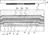
In this execution mode, explanation is used for the manufacturing step of the thin-film transistor of liquid crystal indicator with reference to Figure 1A to Fig. 6.Figure 1A to Fig. 3 C is the sectional view that the manufacturing step of thin-film transistor is shown, and Fig. 4 is the vertical view of the join domain of thin-film transistor and a pixel electrode in the pixel.In addition, Fig. 5 is the sequential chart that the film build method of microcrystalline sillicon film is shown, and Fig. 6 is the sectional view that a configuration example of the plasma CVD apparatus that can provide two above RF powers with different frequency to produce glow discharge plasma is shown.
About having the thin-film transistor of microcrystalline semiconductor film, n type thin-film transistor has than the high field-effect mobility of p type thin-film transistor, therefore is more suitable for being used for drive circuit.Preferably, on same substrate, form the thin-film transistor of same polarity, to reduce manufacturing step.Here, use n channel-type thin-film transistor to describe.
Shown in Figure 1A, on substrate 50, form gate electrode.Substrate 50 can use through utilizing alkali-free glass substrate that fusion method or float glass process make such as barium borosilicate glass, aluminium borosilicate glass, alumina silicate glass.When substrate 50 is female glass, the size of substrate can adopt the first generation (300mm * 400mm), the second generation (400mm * 500mm), the third generation (550mm * 650mm), the 4th generation (730mm * 920mm), the 5th generation (1000mm * 1200mm), the 6th generation (2450mm * 1850mm), the 7th generation (1870mm * 2200mm), the 8th generation (2000mm * 2400mm), the 9th generation (2450mm * 3050mm), the tenth generation (2850mm * 3050mm), or the like.
Gate electrode forms through metal material or its alloy material that uses titanium, molybdenum, chromium, tantalum, tungsten, aluminium etc.Can on substrate 50, form conducting film through using sputtering method, vacuum vapour deposition or CVD method, on this conducting film, form mask, and use this mask etching conducting film, to form gate electrode through use photoetching technique or ink-jet method.Gate electrode can also form the injection of electrical-conductive nanometer glue and the roasting of silver, gold, copper etc. through using ink-jet method.In addition, as the being adjacent to property that improves gate electrode and prevent the barrier metal of basad diffusion, the nitride film of above-mentioned metal material can be set between substrate 50 and gate electrode.Here, the Etching mask etching that use forms through first photomask is formed on the lamination of the conducting film on the substrate 50, to form gate electrode.
As the object lesson of gate electrode structure, can be as the aluminium film laminated of the first conductive layer 51a molybdenum film, to prevent distinctive hillock of aluminium or electromigration as the second conductive layer 51b.Because shown in this execution mode through using the manufacturing of large tracts of land substrate having the example of the display unit of large display screen, so the gate electrode of the first conductive layer 51a that uses range upon range of to constitute by the low aluminium of resistance and its thermal endurance second conductive layer 51b higher than the first conductive layer 51a.In addition, can adopt the aluminium film to be sandwiched in the three-decker between the molybdenum film.As other examples of gate electrode structure, can enumerate the structure that the structure of molybdenum film is arranged, the structure of titanium nitride film is arranged and the nitrogenize tantalum film is arranged in the copper film laminated in the copper film laminated in the copper film laminated.
Owing on gate electrode, form semiconductor film or wiring, preferably its end is processed as taper to prevent fracture.Though not shown, in above-mentioned steps, can also form the wiring that is connected with gate electrode simultaneously.
Then, on the second conductive layer 51b, form gate insulating film 52a, 52b and 52c successively as the upper strata gate electrode.
Here, oxygen silicon nitride membrane refers to that oxygen content is more than the material of nitrogen content on it is formed, and it comprises oxygen, nitrogen, Si and hydrogen, and its concentration is following: the oxygen of 55 to 65 atom %; The nitrogen of 1 to 20 atom %; The Si of 25 to 35 atom %; And the hydrogen of 0.1 to 10 atom %.On the other hand, silicon oxynitride film refers to that nitrogen content is more than the material of oxygen content on it is formed, and it comprises oxygen, nitrogen, Si and hydrogen, and its concentration is following: the oxygen of 15 to 30 atom %; The nitrogen of 20 to 35 atom %; The Si of 25 to 35 atom %; And the hydrogen of 15 to 25 atom %.
Ground floor gate insulating film and second layer gate insulating film all are thicker than 50nm.As the ground floor gate insulating film, preferably use silicon nitride film or silicon oxynitride film, spread from substrate to prevent impurity (for example alkali metal etc.).The ground floor gate insulating film not only can prevent the oxidation of gate electrode, but also can under the situation of use aluminium as gate electrode, prevent hillock.In addition, the thickness of the 3rd layer of gate insulating film that contacts with microcrystalline semiconductor film is preferably about 1nm greater than 0nm and below the 5nm.The 3rd layer of gate insulating film is in order to improve with the being adjacent to property of microcrystalline semiconductor film.In addition, through using silicon nitride film as the 3rd layer of gate insulating film, can prevent by after the oxidation of the microcrystalline semiconductor film that causes of the heat treatment carried out or laser radiation.For example, when under oxygen content dielectric film how and microcrystalline semiconductor film state of contact, heat-treating, may make the microcrystalline semiconductor film oxidation.
Moreover the microwave plasma CVD equipment that preferred frequency of utilization is 1GHz forms gate insulating film.Oxygen silicon nitride membrane through using microwave plasma CVD equipment to form, the resistance to pressure of silicon oxynitride film are high, thereby can improve the reliability of thin-film transistor.
In this execution mode, preferably,, carry out substrate pretreatment through carrying out folk prescription or the both sides in the processing of rare gas Cement Composite Treated by Plasma and hydrogen plasma, carry out film forming then and handle.In addition, the preferred film of coating and gate insulating film identical type in reative cell in advance.This is to sneak into gate insulating film for metal impurities that prevent reaction chamber wall etc.
As reacting gas, use silane etc. silane gas, comprise the gas of oxygen or nitrogen.And, apply HF frequency band (3MHz to 30MHz is typically 13.56MHz) and the RF power of VHF frequency band (30MHz to 300MHz) produces glow discharge plasma through overlapping.Through applying the different RF power of frequency band, can improve plasma density, and can improve the substrate inner evenness of plasma density.The film-forming temperature of gate insulating film is preferably 200 ℃ to 400 ℃, can form densification and the high dielectric film of resistance to pressure through improving plasma density.The sectional view of this moment is equivalent to Figure 1A.
Here, though form gate insulating film, under the situation of the switch element that is used as liquid crystal indicator, can constitute by a individual layer by silicon nitride film owing to carry out AC driving with three-decker.
Then, preferably, after forming gate insulating film, do not contact atmosphere ground carrying substrate, with the vacuum chamber that forms gate insulating film vacuum chamber inequality in formation microcrystalline semiconductor film 53.
Below, the step that forms microcrystalline semiconductor film 53 is described with reference to Fig. 5.In Fig. 5; Being initial step with reative cell from the step that atmospheric pressure is vented to vacuum (vacuum exhaust 200), various processing of carrying out after illustrating respectively with the seasonal effect in time series mode such as precoating 201, substrate move into 202, substrate pretreatment 203, film forming handle 204, substrate is taken out of 205, purified 206.But, be not limited to from atmospheric pressure and be vented to vacuum, reduce the viewpoint of final vacuum degree from a large amount of productions or with the short time, reative cell preferably remains vacuum degree to a certain degree always.
In this execution mode,, the vacuum degree in the vacuum chamber before substrate is moved into is higher than 10 for being set at
-5The vacuum degree of Pa is carried out the ultra high vacuum exhaust.This step is equivalent to the vacuum exhaust 200 among Fig. 5.Under the situation of carrying out above-mentioned ultra high vacuum exhaust, preferably utilize turbomolecular pump and cryopump, promptly utilize turbomolecular pump to carry out exhaust, and utilize cryopump to carry out vacuum exhaust.In addition, preferably reative cell is carried out heat treated, to outgas from inwall.Also make the heater work of heated substrate make temperature stabilization.The heating-up temperature of substrate is more than 100 ℃ below 300 ℃, is preferably more than 120 ℃ below 220 ℃.
Then, before moving into substrate, carry out precoating 201, to form silicon fiml as the inwall coverlay.As precoating 201; Produce plasma to remove through introducing hydrogen or rare gas attached to the gas on the inwall of reative cell (Atmospheric components of oxygen and nitrogen etc. or be used for etching gas that reative cell is purified); Introduce silane gas then, produce plasma.Because silane gas and oxygen or moisture etc. react,, can remove oxygen or moisture in the reative cell so produce the silane plasma through flowing through silane gas.In addition, through carrying out precoating 201, the metallic element that can prevent to constitute the parts of reative cell is sneaked in the microcrystalline sillicon film as impurity.In other words, cover in the reative cell, can prevent that reative cell is interior by plasma etching, and can reduce the impurity concentration that is included in the microcrystalline sillicon film that forms afterwards through using silicon.Precoating 201 comprises uses the processing that covers reaction chamber wall with the film that will be deposited in the film identical type on the substrate.
After precoating 201, carry out substrate and move into 202.Be stored in the load chamber that has been carried out vacuum exhaust owing to will pile up the substrate of microcrystalline sillicon film, so the vacuum degree in the reative cell is significantly worsened even move into substrate.
Then, carry out substrate pretreatment 203.Substrate pretreatment 203 is when forming microcrystalline sillicon film, especially effectively to handle, and therefore preferably carries out substrate pretreatment 203.In other words, when on the surface of the surface of glass substrate surface, dielectric film or amorphous silicon, forming microcrystalline sillicon film through plasma CVD method, sometimes in piling up initial stage owing to impurity or lattice mismatch etc. causes forming amorphous layer.Remove this amorphous layer for the thickness that reduces this amorphous layer or living if possible as far as possible, preferably carry out substrate pretreatment 203.As substrate pretreatment, preferably carry out rare gas Cement Composite Treated by Plasma or hydrogen plasma and handle, perhaps carry out this two kinds of processing.As the rare gas Cement Composite Treated by Plasma, preferred big rare gas element such as argon, krypton or the xenon of service quality number.This is because through utilizing the sputter effect to remove the cause attached to the impurity of lip-deep oxygen, moisture, organic substance or metallic element etc.It is for through utilizing hydroperoxyl radical to remove to be adsorbed on lip-deep above-mentioned impurity and clean effective by film formation surface through utilizing etching action to dielectric film or amorphous silicon film to form that hydrogen plasma is handled.In addition, handle, can expect to promote the caryogenic effect of crystallite through carrying out rare gas Cement Composite Treated by Plasma and hydrogen plasma.
From promoting the caryogenic viewpoint of crystallite, shown in the dotted line among Fig. 5 207, it is effective continuing to provide the rare gas of argon etc. in the initial stage in the film forming of microcrystalline sillicon film.
After carrying out substrate pretreatment 203, the film forming that forms microcrystalline sillicon film handles 204.In this execution mode, form the bottom of the microcrystalline sillicon film of gate insulating film near interface under first membrance casting condition that quality is good in that film forming speed is low, under the second high membrance casting condition of film forming speed, pile up the top of microcrystalline sillicon film then.For example,, come film forming,, continue to form microcrystalline semiconductor film under the not overlapping membrance casting condition that applies at the 3rd RF power that applies 3MHz to 30MHz as second membrance casting condition through overlapping frequency two RF powers inequality that apply as first membrance casting condition.In addition; As first membrance casting condition; Overlapping apply first RF power, with and electric power greater than second RF power of this first RF power; As second membrance casting condition, continue apply three RF power of its electric power greater than said first membrance casting condition, with and the membrance casting condition of electric power less than the 4th RF power of the 3rd RF power under form microcrystalline semiconductor film.Notice that the frequency of the 3rd RF power is identical with first RF power, and the frequency of the 4th RF power is identical with second RF power.
As long as the film forming speed of second membrance casting condition is higher than the film forming speed of first membrance casting condition, just have no particular limits.In this execution mode; Use to utilize the plasma CVD apparatus of the glow discharge plasma that generates through the RF power of overlapping RF power that applies HF frequency band (3MHz to 30MHz is typically 13.56MHz) and VHF frequency band (about 30MHz to 300MHz).Fig. 7 illustrates with the RF power of the RF power of HF frequency band and VHF frequency band an example of the waveform when overlapping.
Say that typically microcrystalline sillicon film can be through using hydrogen dilution silane such as SiH
4Or Si
2H
6Realize that plasma generates and forms.Except silane and the hydrogen, can also use one or more rare gas units that are selected from helium, argon, krypton, the neon usually to dilute, to form microcrystalline semiconductor film.The flow-rate ratio with respect to the hydrogen of silane of this moment is more than 12 times below 1000 times, is preferably more than 50 times below 200 times more preferably 100 times.In addition, can use SiH
2Cl
2, SiHCl
3, SiCl
4, SiF
4Deng the replacement silane.
Helium is being added under the situation of material gas; Because the ionization energy of helium is the highest in all gas, i.e. 24.5eV, its metastable state is positioned at the energy level of the about 20eV lower a little than this ionization energy; So in during discharge sustain, only need for ionization about the 4eV of its difference.Therefore, the discharge ionization voltage value is also minimum in all gas.Because above-mentioned characteristic, helium can stably keep plasma.In addition, owing to can form uniform plasma,, also can play the effect of the homogenizing that realizes plasma density even piling up the area of the substrate of microcrystalline sillicon film increases.
Can also be with the hydride such as the CH of carbon
4Or C
2H
6, germne or fluoridize germanium such as GeH
4Or GeF
4Be mixed in the gas of silane etc., bandwidth is adjusted into 1.5 to 2.4eV or 0.9 to 1.1eV.Through adding carbon or germanium to silicon, can change the temperature characterisitic of TFT.
Here, first membrance casting condition is following: through use hydrogen and/or rare gas with the silane dilution for surpassing below 100 times and 2000 times, the heating-up temperature of substrate is more than 100 ℃ and is lower than 300 ℃, is preferably more than 120 ℃ below 220 ℃.In order to promote the growth of microcrystal silicon, preferred film forming under the temperature below 220 ℃ more than 120 ℃.
To under first membrance casting condition, be illustrated in Figure 1B by the sectional view after the film forming.On gate insulating film 52c, be formed with low and the microcrystalline semiconductor film 23 that quality is good of film forming speed.The increase of the conducting electric current of the TFT that forms after the article of the microcrystalline semiconductor film 23 that should under first membrance casting condition, obtain are verified and the raising of field-effect mobility are contributed, and therefore importantly reduce oxygen concentration fully, so that the oxygen concentration in the film is set at 1 * 10
17Below/the cm.In addition, through above-mentioned steps, except oxygen, can also reduce the nitrogen of sneaking in the microcrystalline semiconductor film and the concentration of carbon.Therefore can prevent the n typeization of microcrystalline semiconductor film.
Then, replace first membrance casting condition to improve film forming speed, to form microcrystalline semiconductor film 53 through adopting second membrance casting condition.The sectional view of this moment is equivalent to Fig. 1 C.The thickness of microcrystalline semiconductor film 53 can be 50nm to 500nm (being preferably 100nm to 250nm).Notice that in this execution mode, the film formation time of microcrystalline semiconductor film 53 is included between first film forming stage of film forming under first membrance casting condition and between second film forming stage of film forming under second membrance casting condition.Though can the film that be called first microcrystalline semiconductor film at the film that obtains under first membrance casting condition and will under second membrance casting condition, obtain be called second microcrystalline semiconductor film; But the interface of first microcrystalline semiconductor film after film forming and second microcrystalline semiconductor film is indeterminate, and the stack membrane that therefore obtains through change condition between film forming stage is called as microcrystalline semiconductor film.
In this execution mode, second membrance casting condition is following: is more than 12 times below 100 times through using hydrogen and/or rare gas with the silane dilution, and the heating-up temperature of substrate is more than 100 ℃ and is lower than 400 ℃, is preferably below 220 ℃.In this execution mode; Flow through increasing silane gas makes the film forming speed of second membrance casting condition higher than first membrance casting condition; But it is had no particular limits, also can make the film forming speed of second membrance casting condition higher through the condition of RF power that change applies RF power and the VHF frequency band of HF frequency band than first membrance casting condition.For example; Under first membrance casting condition; The overlapping electric power of output waveform of high frequency electric source of output waveform and VHF frequency band that kind as shown in Figure 7 is carried out the high frequency electric source of HF frequency band applies; And under second membrance casting condition, the conducting and ending that kind as shown in Figure 8 is carried out the RF power of VHF frequency band repeatedly realizes that impulse hunting is to obtain the partly overlapping waveform of one of which.
Then, after forming microcrystalline sillicon film through second membrance casting condition, the supply that stops material gas such as silane or hydrogen and RF power is carried out substrate and is taken out of 205.Next substrate is being proceeded under the situation that film forming handles, got back to substrate and move into 202 step and carry out same processing.In order to remove, purify 206 attached to film in the reative cell or powder.
As purifying 206, through introducing with NF
3, SF
6For the etching gas of representing carries out plasma etching.In addition, even do not utilize the plasma can etched gas such as ClF through introducing yet
3Carry out.Purify 206 preferably the substrate heater by and the state that reduced of process chamber inner wall temperature under carry out.This is the generation for the secondary product of reaction that suppresses to be caused by etching.Purifying after 206, getting back to precoating 201, next substrate is being carried out above-mentioned same processing, getting final product.
Here, a configuration example of the plasma CVD apparatus that is used for forming gate insulating film or microcrystalline sillicon film is illustrated in Fig. 6, a plurality of RF powers are applied to this plasma CVD equipment.
RF power feed unit 103 is attached to first electrode 101, and earthing potential offers second electrode 102, and have can load substrates structure.First electrode 101 is by insulating material 116 and reative cell 100 insulated separation, and constitutes and do not miss RF power.Note; First electrode 101 and second electrode 102 of capacitive coupling type (parallel plate-type) structure adopted in expression in Fig. 6; But as long as can adopt other structures such as induction coupled mode at the reative cell 100 inner glow discharge plasmas that generate through applying two or more different RF powers.
The RF power that first high frequency electric source 104 is provided utilizes its wavelength to be approximately the above high frequency of 10m, utilizes the 3MHz to 30MHz as the HF frequency band, is typically 13.56MHz.The RF power that second high frequency electric source 105 is provided utilizes the VHF frequency band, and its wavelength promptly utilizes the RF power of 30MHz to 300MHz approximately less than 10m.
The wavelength of the RF power that first high frequency electric source 104 is provided has the length more than 3 times on one side of first electrode 101, and the wavelength applications of the high frequency that second high frequency electric source 105 is provided is shorter than the wavelength of the high frequency that first high frequency electric source 104 provided.Offer first electrode 101 through the RF power that will not cause the standing surface wave influence and produce glow discharge plasma; And the densification that provides the RF power that belongs to the VHF frequency band to realize glow discharge plasma, form on the large tracts of land substrate of 2000mm evenly and the high film of film quality thereby can surpass on its long limit.
Fig. 7 illustrates the instance of the waveform when the RF power of the RF power that makes first high frequency electric source 104 and second high frequency electric source 105 is overlapping.The output waveform of second high frequency electric source 105 of the output waveform of first high frequency electric source 104 through making the frequency of using HF frequency band (being typically 13.56MHz) and the frequency of Application V HF frequency band is overlapping; Realize the densification of plasma, and can improve the inner evenness of plasma density and do not receive the influence of standing surface wave.The instance of the power supply that Fig. 8 illustrates apply pulse vibration as sketch map during as second high frequency electric source 105.Through the RF power of VHF frequency band is provided with pulse mode, can prevent that when film forming powder is grown undesiredly in gas phase.In order to prevent the powder growth, need to consider the mean residence time of gas molecule, but the frequency of oscillation of pulse is set at about 1 to 100kHz, get final product.
Fig. 9 representes other structures of first electrode 101.First electrode 101 provides the first electrode 101b of RF power to constitute by the first electrode 101a that RF power is provided from first high frequency electric source 104 with from second high frequency electric source 105.The first electrode 101a and the first electrode 101b are provided with the hole respectively and form the broach shape of interlock each other on the face with respect to substrate, and are separated by insulating material 116, contact with each other to prevent adjacent electrode.Structure shown in Figure 9 can replace first electrode 101 shown in Figure 6, and can obtain identical effect.
The exhaust unit 109 that is connected to reative cell 100 has the function of carrying out vacuum exhaust and under flowing into the situation of reacting gas, remaining predetermined pressure in reative cell 100.Structure as exhaust unit 109 comprises butterfly valve 117, pilot valve 118, turbomolecular pump 119, dried pump 120 etc.Under the situation of parallel connection configuration butterfly valve 117 and pilot valve 118, make pilot valve 118 work through closing butterfly valve 117, the exhaust velocity that can control reacting gas remains predetermined scope with the pressure of reative cell 100.In addition, through making 117 work of the high butterfly valve of conductibility, can carry out high vacuum exhaustion.
For making vacuum degree be higher than 10
-5Pa and carrying out under the situation of ultra high vacuum exhaust preferably uses cryopump 121.It is also effective that vacuum exhaust is carried out in two turbo-molecular series connections of pumps.In addition, carrying out under the situation of vacuum exhaust till final vacuum degree becomes ultra high vacuum, can carry out mirror finish, and the heater that is provided for toasting is to suppress discharging gas from inwall the inwall of reative cell 100.
Then, after forming microcrystalline semiconductor film 53, preferably do not contact atmosphere ground carrying substrate, come with the vacuum chamber that forms microcrystalline semiconductor film 53 vacuum chamber inequality in formation resilient coating 54.Through the vacuum chamber that forms resilient coating 54 is provided in addition, can the vacuum chamber of formation microcrystalline semiconductor film 53 be used as before introducing substrate and arrive the dedicated processes chamber of ultra high vacuum, thus the time that can as far as possible suppress contaminating impurity and shortening arrival ultra high vacuum.For arriving under the situation that ultra high vacuum toasts, need the long period for obtaining the low and stable status of process chamber inner wall temperature, be effective especially therefore.In addition, through vacuum chamber inequality is provided respectively, can change the frequency of RF power respectively according to the film that goes for.
As resilient coating 54, also can through with amorphous semiconductor as target and use hydrogen or rare gas carries out sputter and forms amorphous semiconductor film.At this moment, through with ammonia, nitrogen or N
2O is included in the atmosphere, can form the amorphous semiconductor film that comprises nitrogen.In addition, through comprising the gas (F of fluorine, chlorine, bromine or iodine
2, Cl
2, Br
2, I
2, HF, HCl, HBr, HI etc.) be included in the atmosphere, can form the amorphous semiconductor film that comprises fluorine, chlorine, bromine or iodine.
After form in the step in source region and drain region, the part of resilient coating 54 is etched.Therefore, resilient coating 54 is preferably formed into the residual thickness of its part under above-mentioned situation, not expose microcrystalline semiconductor film 53.Say that typically resilient coating 54 forms to have below the above 400nm of 100nm, be preferably the thickness below the above 300nm of 200nm.The display unit that applies voltage height (for example being approximately 15V) at thin-film transistor; Typically be in the liquid crystal indicator; Through the thickness setting with resilient coating 54 is in the above-mentioned scope; Can improve resistance to pressure, thereby even high voltage is applied to the degeneration that thin-film transistor also can be avoided thin-film transistor.
In addition, resilient coating 54 is not added with impurity such as phosphorus or the boron etc. of giving a conduction type.In order to prevent that impurity is diffused into microcrystalline semiconductor film 53 from the semiconductor film 55 that is added with the impurity of giving a conduction type, resilient coating 54 is used as the barrier layer.Under the situation that resilient coating 54 is not set, if microcrystalline semiconductor film 53 contacts with the semiconductor film that is added with the impurity of giving a conduction type 55, then have after etching step or heat treated in impurity move, thereby be difficult to control the problem of threshold voltage.
Through on the surface of microcrystalline semiconductor film 53, forming resilient coating 54, can prevent to be included in the autoxidation of the grain surface in the microcrystalline semiconductor film 53.Especially in amorphous semiconductor and zone that micromeritics contacts, produce the crack because of local stress easily.Crystal grain is oxidized when this crack contacts with oxygen, thereby forms silica.
53 big (energy gap of amorphous semiconductor film is 1.6 to 1.8eV than microcrystalline semiconductor film as the energy gap of the resilient coating 54 of amorphous semiconductor film; And the energy gap of microcrystalline semiconductor film 53 is 1.1 to 1.5eV); Its resistance is high, and its mobility is low, and promptly 1/5 of microcrystalline semiconductor film 53 to 1/10.Therefore, after in the thin-film transistor that forms, be formed on resilient coating between source region and drain region and the microcrystalline semiconductor film 53 as high resistance area, and microcrystalline semiconductor film 53 is as the channel formation region territory.Therefore, can reduce the cut-off current of thin-film transistor.Under with the situation of this thin-film transistor, can improve the contrast of display unit as the switch element of display unit.
Preferably, on microcrystalline semiconductor film 53, through plasma CVD method with more than 300 ℃ and be lower than 400 ℃ underlayer temperature and form resilient coating 54.Handle through above-mentioned film forming, can hydrogen be offered microcrystalline semiconductor film 53, thereby obtain and make the identical effect of microcrystalline semiconductor film 53 hydrogenations.In other words,, can hydrogen be diffused into microcrystalline semiconductor film 53 through on microcrystalline semiconductor film 53, piling up resilient coating 54, thereby to the dangling bonds end-blocking.In addition, can when forming resilient coating 54, carry out the annealing of microcrystalline semiconductor film 53, thereby can improve film quality.Especially; Though the film that obtains through second membrance casting condition have its film forming speed than first membrance casting condition high and its crystallinity than the low characteristic of crystallinity that obtains through first membrance casting condition; But, can improve the film quality of crystallinity etc. through when forming resilient coating, annealing.In addition; Through when forming resilient coating 54, annealing; The change (change of threshold voltage etc.) of the TFT characteristic in the reliability test of voltage can also be suppressed to apply repeatedly, thereby its reliability can be obtained than the high TFT of TFT that amorphous silicon film is mainly used in the channel formation region territory.
Then, after forming resilient coating 54, preferably do not contact atmosphere ground carrying substrate, come with the vacuum chamber that forms resilient coating 54 vacuum chamber inequality in formation be added with the semiconductor film 55 of the impurity of giving a conduction type.The sectional view of this moment is equivalent to Fig. 1 D.Through with the vacuum chamber that forms resilient coating 54 vacuum chamber inequality in form the semiconductor film 55 that is added with the impurity of giving a conduction type, can prevent that the impurity of giving a conduction type from sneaking into when forming resilient coating.
About the semiconductor film 55 that is added with the impurity of giving a conduction type, under the situation that forms n channel-type thin-film transistor, can add phosphorus as typical impurity element, and can be with PH
3Deng foreign gas add silane to.In addition, under the situation that forms p channel-type thin-film transistor, can add boron as typical impurity element, and can be with B
2H
6Deng foreign gas add silane to.The semiconductor film 55 that is added with the impurity of giving a conduction type can be made up of crystallite semiconductor or amorphous semiconductor.The thickness that is added with the semiconductor film 55 of the impurity of giving a conduction type is below the above 50nm of 2nm.Be added with the thickness of the semiconductor film of the impurity of giving a conduction type through minimizing, can improve productive rate.
Then, shown in Fig. 2 A, on the semiconductor film that is added with the impurity of giving a conduction type 55, form Etching mask 56.Etching mask 56 forms through using photoetching technique or ink-jet method.Here, through using second photomask, make public and develop being coated in resist on the semiconductor film 55 that is added with the impurity of giving a conduction type, to form Etching mask 56.
Then; Through using Etching mask 56 with microcrystalline semiconductor film 53, resilient coating 54 and semiconductor film 55 etchings that are added with the impurity of giving a conduction type, such semiconductor film 63 that forms microcrystalline semiconductor film 61, resilient coating 62 and be added with the impurity of giving a conduction type shown in Fig. 2 B.Then, remove Etching mask 56.
The end sides of microcrystalline semiconductor film 61 and resilient coating 62 tilts, thereby can prevent between the source region and drain region and the microcrystalline semiconductor film 61 that are formed on the resilient coating 62, to produce leakage current.Can also prevent between source electrode and drain electrode and microcrystalline semiconductor film 61, to produce leakage current.The angle of inclination of the end sides of microcrystalline semiconductor film 61 and resilient coating 62 is 30 ° to 90 °, is preferably 45 ° to 80 °.Through adopting above-mentioned angle, the source electrode that can prevent to cause or the disconnection of drain electrode by step shape.
Then, shown in Fig. 2 C, cover the semiconductor film 63 and the gate insulating film 52c ground that are added with the impurity of giving a conduction type and form conducting film 65a to 65c as conducting film.Conducting film 65a to 65c preferably improves element by aluminium, copper or the thermal endurance that is added with silicon, titanium, neodymium, scandium, molybdenum etc. or hillock prevents that the individual layer or the lamination of the aluminium alloy of element from constituting.Can also adopt following laminated construction: the nitride formation through using titanium, tantalum, molybdenum, tungsten or these elements contacts the film of a side with the semiconductor film that is added with the impurity of giving a conduction type, and forms aluminum or aluminum alloy above that.Moreover can adopt following laminated construction: the upper surface of aluminum or aluminum alloy and lower surface are clamped by the nitride of titanium, tantalum, molybdenum, tungsten or these elements.Here, the conducting film of these three plies of conducting film 65a to 65c is shown, and following lamination conducting film is shown: conducting film 65a and 65c are made up of the molybdenum film, and conducting film 65b is made up of the aluminium film; Perhaps, conducting film 65a and 65c are made up of titanium film, and conducting film 65b is made up of the aluminium film.Conducting film 65a to 65c forms through sputtering method or vacuum vapour deposition.
Then, shown in Fig. 2 D, on conducting film 65a to 65c, form Etching mask 66 through use the 3rd photomask, and the part of etching conducting film 65a to 65c, to form source electrode and drain electrode 71a to 71c.Through conducting film 65a to 65c is carried out wet etching, conducting film 65a to 65c is selectively etched.Consequently, owing to can form its area source electrode and the drain electrode 71a to 71c littler with isotropic mode etching conducting film than Etching mask 66.
Then, shown in Fig. 3 A, be added with the semiconductor film 63 of the impurity of giving a conduction type, form a pair of source region and drain region 72 through using Etching mask 66 etchings.Moreover in this etching step, the part of resilient coating 62 also is etched.Owing to being etched the resilient coating that is formed with recess (groove), its part is called as resilient coating 73.Can form the recess (groove) of source region and drain region and resilient coating with same step.Be set at through the degree of depth the recess (groove) of resilient coating resilient coating the thickest zone 1/2 to 1/3, can increase the distance in source region and drain region, therefore can reduce the leakage current between source region and the drain region.Afterwards, remove Etching mask 66.
With about etch buffer layer 50nm, to prevent following situation: especially, Etching mask is rotten when being exposed to the plasma that is used for dry ecthing etc., and can not remove in the step at resist and remove fully, thus residual residue.Use Etching mask 66 in the etch processes of the part of conducting film 65a to 65c and in this twice etch processes of etch processes when forming source region and drain region 72; Adopting easy residual residue under the situation of dry ecthing as this twice etch processes, therefore will be when removing residue fully can etched resilient coating forming that to have thick film thickness be effective.In addition, resilient coating 73 can prevent when dry ecthing, to give microcrystalline semiconductor film 61 to bring plasma damage.
Then, shown in Fig. 3 B, form dielectric film 76, this dielectric film 76 covering source electrodes and drain electrode 71a to 71c, source region and drain region 72, resilient coating 73, microcrystalline semiconductor film 61 and gate insulating film 52c.Dielectric film 76 can form with the film build method identical with gate insulating film 52a, 52b and 52c.Notice that dielectric film 76 is that the intrusion for the pollution impurity of the organic substance in atmosphere of preventing to swim, metal object, steam etc. provides, therefore preferably adopt fine and close film.In addition, through silicon nitride film being used for dielectric film 76, can the oxygen concentration in the resilient coating 73 be set at 5 * 10
19Atoms/cm
3Below, be preferably 1 * 10
19Atoms/cm
3Below.
Shown in Fig. 3 B; The end in the end of source electrode and drain electrode 71a to 71c and source region and drain region 72 is inconsistent and stagger each other; The distance of the end of source electrode and drain electrode 71a to 71c increases, thereby can prevent leakage current or the short circuit between source electrode and the drain electrode.In addition; Because the end of source electrode and drain electrode 71a to 71c and the end in source region and drain region 72 are inconsistent and stagger each other; Do not concentrate so in the end in source electrode and drain electrode 71a to 71c and source region and drain region 72, electric field does not take place, thereby can prevent the leakage current between gate electrode and source electrode and the drain electrode 71a to 71c.Thus, can make high reliability and high withstand voltage thin-film transistor.
Through above-mentioned steps, can form thin-film transistor 74.
In the thin-film transistor shown in this execution mode; In the gate electrode laminated gate insulating film, microcrystalline semiconductor film, resilient coating, source region and drain region, source electrode and drain electrode, wherein be cushioned layer and cover as the surface of the microcrystalline semiconductor film in channel formation region territory.In addition, in the part of resilient coating, be formed with recess (groove), and the zone beyond this recess is covered by source region and drain region.In other words, certain distance is arranged between source region and drain region, therefore can reduce the leakage current between source region and the drain region owing to be formed on the recess in the resilient coating.In addition, because the part through etch buffer layers forms recess, thus can remove the etch residue that in the step that forms source region and drain region, produces, thus the source region that can avoid causing and the leakage current (parasitic channel) in drain region by residue.
In addition, between the microcrystalline semiconductor film that is used as the channel formation region territory and source region and drain region, be formed with resilient coating.The surface of microcrystalline semiconductor film is cushioned layer and covers.High-resistance resilient coating extends between microcrystalline semiconductor film and source region and the drain region, thereby can reduce the leakage current that is created in the thin-film transistor, and can suppress owing to applying the degeneration that high voltage causes.In addition, resilient coating, microcrystalline semiconductor film, source region and drain region all are formed on the zone with gate electrode.Therefore, can be described as the structure of the influence of the end shape that does not receive gate electrode.Have at gate electrode under the situation of laminated construction; If in its lower floor, use aluminium; Then may expose aluminium and produce hillock in the side of gate electrode; But through adopting source region and drain region also not to be overlapped in the structure of gate electrode end, can prevent with gate electrode side overlapping areas in be short-circuited.In addition; Since on the surface of microcrystalline semiconductor film, be formed with its surface by the amorphous semiconductor film of hydrogen end-blocking as resilient coating; So can prevent the oxidation of microcrystalline semiconductor film, and can prevent that the etch residue that in the step that forms source region and drain region, produces from sneaking into microcrystalline semiconductor film.Thus, can obtain the good and resistance to pressure good film transistor of electrical characteristics.
In addition, the channel length of thin-film transistor can be dwindled, thereby the area of plane of thin-film transistor can be dwindled.
Then, utilize the part of the Etching mask etching dielectric film 76 that the 4th photomask forms, form contact hole, and be formed on the pixel electrode 77 that contacts with source electrode or drain electrode 71c in this contact hole through use.Fig. 3 C is equivalent to along the sectional view of the dotted line A-B of Fig. 4.
As shown in Figure 4, the end in source region and drain region 72 is positioned at the outside of the end of source electrode and drain electrode 71c.In addition, the end of resilient coating 73 is positioned at the outside of the end in source electrode and drain electrode 71c, source region and drain region 72.Side in source electrode and the drain electrode has the opposing party's in encirclement source electrode and the drain electrode shape (specifically, U word shape, C word shape).Therefore, can increase the area in the zone that charge carrier moves, thereby the magnitude of current can increase, and can dwindle the area of thin-film transistor.In addition, because microcrystalline semiconductor film, source electrode and drain electrode layer are stacked on the gate electrode,, thereby can suppress the reduction of coverage and the generation of leakage current so the concavo-convex caused negative effect of gate electrode is few.Notice that the side in source electrode and the drain electrode is also as source wiring or drain electrode wiring.
In addition, can use the conduction constituent that comprises conducting polymer (being also referred to as conducting polymer) to form pixel electrode 77.Preferably, be that 10000 Ω/below the, the light transmittance among the wavelength 550nm is more than 70% through the sheet resistance (sheet resistance) that uses the pixel electrode that the conduction constituent forms.In addition, the resistivity that is included in the conducting polymer of conduction in the constituent is below the 0.1 Ω cm.
As conducting polymer, can use so-called pi-electron conjugated system conducting polymer.For example, can enumerate polyaniline or derivatives thereof, polypyrrole or derivatives thereof, polythiophene or derivatives thereof or these two or more copolymers etc.
Here, as pixel electrode 77, after forming indium tin oxide film, resist is coated on the indium tin oxide film through sputtering method.Then, through utilizing the 5th photomask that resist is made public and developing, to form Etching mask.Then, use Etching mask etching indium tin oxidation film, to form pixel electrode 77.
Through above-mentioned steps, can form the component substrate that is applicable to display unit.
In this execution mode, an example of the multiple-chamber type plasma CVD apparatus of the gate insulating film that be fit to form constitutes the TFT shown in the execution mode 1, microcrystalline semiconductor film, n+ layer is shown.
Figure 10 illustrates an example of the multiple-chamber type CVD equipment with a plurality of reative cells.This equipment comprises common chamber 123, load/unload chamber 122, the first reative cell 100a, the second reative cell 100b, the 3rd reative cell 100c.Each reative cell is taken out of/moved into to the substrate that is placed in the box 124 of load/unload chamber 122 by the carrying mechanism 126 of common chamber 123, and adopt single chip mode.Between common chamber 123 and each chamber, be provided with gate valve 125, interfere each other not make the processing in each reative cell.
Each reative cell is distinguished according to formed film kind.For example; In the first reative cell 100a, form dielectric film such as gate insulating film; In the second reative cell 100b, form microcrystalline semiconductor layer as raceway groove, and in the 3rd reative cell 100c range upon range of resilient coating, as a conductive type impurity semiconductor layer of source electrode and drain electrode.Certainly, the number of reative cell is not limited to this, can increase arbitrarily as required or reduce.In addition, can in a reative cell, form a film, perhaps in a reative cell, form a plurality of films.
As other examples; Can in the first reative cell 100a, form dielectric film such as gate insulating film; In the second reative cell 100b, form microcrystalline semiconductor layer and resilient coating, and in the 3rd reative cell 100c, form a conductive type impurity semiconductor layer as source electrode and drain electrode as raceway groove.
In each reative cell, be connected with turbomolecular pump 119 and dried pump 120 as exhaust unit.Exhaust unit is not limited to the combination of above-mentioned vacuum pump, as long as can be vented to about 10
-5Pa to 10
-1The vacuum degree of Pa just can be used other vacuum pumps.In addition, the second reative cell 100b that forms microcrystalline semiconductor film is connected with cryopump 121, to be vented to ultra high vacuum.Between exhaust unit and each reative cell, be provided with butterfly valve 117, can interdict vacuum exhaust thus, and by pilot valve 118 control exhaust velocities, to adjust the pressure of each reative cell.Notice that the combination of exhaust unit shown in Figure 10 is an example, and it is had no particular limits.
The RF power feed unit 103 that is used for producing glow discharge plasma is connected to each reative cell.RF power feed unit 103 comprises high frequency electric source and adaptation.In the case, through likewise using first high frequency electric source 104, second high frequency electric source 105, first adaptation 106 and second adaptation 107 to constitute RF power feed units 103, can form the high film of uniformity with execution mode 1.The structure of plasma CVD apparatus is set according to the size (550mm * 650mm of the 300mm * 400mm of the first generation, the 400mm * 500mm of the second generation, the third generation, the 730mm * 920mm in the 4th generation, the 1000mm * 1200mm in the 5th generation, the 2450mm * 1850mm in the 6th generation, the 1870mm * 2200mm in the 7th generation, the 2000mm * 2400mm in the 8th generation, the 2450mm * 3050mm in the 9th generation, the 2850mm * 3050mm in the tenth generation etc.) of various glass substrate, thereby can have the high film of formation uniformity on the substrate of virtually any size.
Shown in this execution mode, use a plurality of reative cells shown in Figure 10, these a plurality of reative cells are connected by common chamber, thereby can not contact a plurality of layers inequality of atmosphere laminated.
This execution mode can freely make up with execution mode 1.
Execution mode 3
In this execution mode, the manufacturing step of the thin-film transistor of the multiple-chamber type CVD equipment that employing and the Figure 10 shown in the execution mode 2 are inequality is described with reference to Figure 11.Figure 10 is the equipment with three reative cells, and Figure 11 is the vertical view with multiple-chamber type CVD equipment of four reative cells.
Figure 11 illustrates the structure that multiple-chamber type CVD equipment shown in Figure 10 is provided the 4th reative cell 100d.In Figure 11, the part identical with Figure 10 used same Reference numeral, detailed.In addition, the combination of exhaust unit shown in Figure 11 is an example, and it is had no particular limits.
Gas feed unit 108b is connected to the 4th reative cell 100d.The structure of RF power feed unit and exhaust unit is identical with Figure 10.Each reative cell can be distinguished according to formed film kind.For example; Can in the first reative cell 100a, form dielectric film such as gate insulating film; In the second reative cell 100b, form microcrystalline semiconductor layer as raceway groove; In the 4th reative cell 100d, form the protection raceway groove and form resilient coating, and in the 3rd reative cell 100c, form a conductive type impurity semiconductor layer as source electrode and drain electrode with semiconductor layer.Each film has only film-forming temperature (being also referred to as underlayer temperature), therefore can be through using the manageable film-forming temperature of each reative cell respectively.Moreover, owing to can be concatenated to form the film of identical type, so can eliminate the influence of the residual impurity thing that causes by film forming.
In Figure 11, switch 127 is arranged at the second reative cell 100b, to control the introducing of first RF power and second RF power.Conducting through control switch 127 and ending can change overlapping output waveform.For example, the both sides in switch 127 present output waveform shown in Figure 7 when being in conducting state, and the folk prescription in switch 127 carry out repeatedly conducting and by the time present output waveform shown in Figure 8.
As stated, through switch 127 is set, can enlarge the adjusting range of membrance casting condition.For example, can be through applying after both sides in first RF power and second RF power form microcrystalline semiconductor film, the folk prescription that applies in first RF power and second RF power comes range upon range of resilient coating.
This execution mode can freely make up with execution mode 1 or 2.
Below, with reference to Figure 12 A to Figure 16 C explanation and execution mode 1 method of manufacturing thin film transistor inequality.Here, the step of making thin-film transistor through the technology that adopts its photomask number to lack than execution mode 1 is shown.
With the Figure 1A shown in the execution mode 1 likewise, on substrate 50, form conducting film, and through using the part of Etching mask etching conducting film, to form gate electrode 51.This Etching mask is through applying resist and utilizing the lithography step of first photomask to form on conducting film.Here, inequality with execution mode 1, the example that conducting film is made up of individual layer is shown.Then, through using plasma CVD apparatus shown in Figure 6, on gate electrode 51, form gate insulating film 52a, 52b and 52c successively.
Then, with the Figure 1B shown in the execution mode 1 likewise, under first membrance casting condition, form microcrystalline semiconductor film 23.Then, through in identical process chamber with the second membrance casting condition film forming, likewise use plasma CVD apparatus shown in Figure 6 to form microcrystalline semiconductor film 53 with Fig. 1 C in the execution mode 1.Then, with Fig. 1 D in the execution mode 1 likewise, on microcrystalline semiconductor film 53, form resilient coating 54 successively, be added with the semiconductor film 55 of the impurity of giving a conduction type.
Then, on the semiconductor film that is added with the impurity of giving a conduction type 55, form conducting film 65a to 65c.Then, shown in Figure 13 A, on conducting film 65a, apply resist 80.
Resist 80 can use eurymeric resist or negative resist.Here, use the eurymeric resist.
Then, through using many gray scale masks 59, light shine resist 80, so that resist 80 is made public as second photomask.
Here, with reference to Figure 12 A to 12D the exposure that utilizes many gray scale masks 59 is described.
Many gray scale masks refer to the mask that can set three exposure levels, and these three exposure levels are exposed portion, intermediate exposures part and unexposed portion.Through carrying out exposure and development step once, can form having the Etching mask of a plurality of (being typically two kinds) thickness area.Therefore, through using many gray scale masks, can reduce the photomask number.
As the exemplary of many gray scale masks, can enumerate the half-tone mask 59b shown in the gray scale mask 59a shown in Figure 12 A and Figure 12 C.
Shown in Figure 12 A, gray scale mask 59a is made up of the substrate with light transmission 163, the light shielding part 164 and the diffraction grating 165 that form above that.In light shielding part 164, the transmitance of light is 0%.On the other hand, diffraction grating 165 can be set at the transmitance that light is controlled at interval below the resolution limiting of the light that is used to make public through the interval with the light transmission portion of slit, point, mesh etc.Periodic slit, point, mesh and aperiodicity slit, point, mesh may be used to diffraction grating 165.
As the substrate with light transmission 163, can use the substrate with light transmission of quartz etc.Light shielding part 164 and diffraction grating 165 can be made up of the light absorbing light screening material of chromium or chromium oxide etc.
Light shine under the situation of gray scale mask 59a, shown in Figure 12 B, in light shielding part 164, light transmission rate 166 is 0%, and in the zone that is not provided with light shielding part 164 and diffraction grating 165, light transmission rate 166 is 100%.In addition, in diffraction grating 165, can light transmission rate be adjusted in 10 to 70% the scope.Light transmission rate in the diffraction grating 165 can be controlled through the interval and the pitch of slit, point or mesh of adjustment diffraction grating.
Shown in Figure 12 C, half-tone mask 59b by the substrate with light transmission 163, form above that half see through portion 167 and light shielding part 168 constitutes.Half sees through portion 167 can use MoSiN, MoSi, MoSiO, MoSiON, CrSi etc.Light shielding part 168 can be made up of the light absorbing light screening material of chromium or chromium oxide etc.
Light shine under the situation of half-tone mask 59b, shown in Figure 12 D, in light shielding part 168, light transmission rate 169 is 0%, and be not provided with light shielding part 168 and half through in the zone of portion 167, and light transmission rate 169 is 100%.In addition, see through in the portion 167, can light transmission rate be adjusted in 10 to 70% the scope half.Half can be according to partly adjusting through the material of portion 167 through the light transmission rate in the portion 167.
Through after the many gray scale masks of use make public, developing, can shown in Figure 13 B, that kind form Etching mask 81 with thickness area inequality.
Then, through using Etching mask 81 with microcrystalline semiconductor film 53, resilient coating 54, the semiconductor film 55 that is added with the impurity of giving a conduction type and conducting film 65a to 65c etching and separation.Consequently, such microcrystalline semiconductor film 61, resilient coating 62, the semiconductor film 63 that is added with the impurity of giving a conduction type and conducting film 85a to 85c of forming shown in Figure 14 A.Figure 14 A is equivalent to the sectional view (beyond the Etching mask 86) along the A-B line of Figure 16 A.
Then, Etching mask 81 is carried out ashing treatment.Consequently, the area of resist dwindles, its thickness attenuation.At this moment, the resist in the zone of thin thickness (with a part of overlapping areas of gate electrode 51) is removed, and shown in Figure 14 A, can form separated Etching mask 86 thus.
Then, through using Etching mask 86 with conducting film 85a to 85c etching and separation.Consequently, that works shown in Figure 14 B forms pair of source electrode and drain electrode 92a to 92c.Through using 86 couples of conducting film 85a to 85c of Etching mask to carry out wet etching, conducting film 85a to 85c is selectively etched.Consequently, owing to can form its area source electrode and the drain electrode 92a to 92c littler with isotropic mode etching conducting film than Etching mask 86.
Then, be added with the semiconductor film 63 of the impurity of giving a conduction type, form a pair of source region and drain region 88 through using Etching mask 86 etchings.Notice that in this etching step, the part of resilient coating 62 also is etched.Its a part of etched resilient coating is called resilient coating 87.In addition, in resilient coating 87, be formed with recess.Can form the recess (groove) of source region and drain region and resilient coating with same step.Here, because through using the part of its area Etching mask 86 etch buffer layers 87 littler, so resilient coating 87 is outstanding to the outside in source region and drain region 88 than Etching mask 81.Then, remove Etching mask 86.In addition, the end in the end of source electrode and drain electrode 92a to 92c and source region and drain region 88 is inconsistent and stagger each other, and the outside of the end of electrode and drain electrode 92a to 92c is formed with the end in source region and drain region 88 in the source.
Figure 14 C is equivalent to along the sectional view of the A-B line of Figure 16 B.Shown in Figure 16 B, the end in source region and drain region 88 is positioned at the outside of the end of source electrode and drain electrode 92c.In addition, the end of resilient coating 87 is positioned at the outside of the end in source electrode and drain electrode 92c, source region and drain region 88.Side in source electrode and the drain electrode has the shape (specifically, U word shape, C word shape) of surrounding the opposing party in source region and the drain region.Therefore, can increase the area in the zone that charge carrier moves, thereby the magnitude of current can increase, and can dwindle the area of thin-film transistor.In addition, because microcrystalline semiconductor film, source electrode and drain electrode layer are stacked on the gate electrode,, and can suppress the reduction of coverage and the generation of leakage current so the concavo-convex caused negative effect of gate electrode is few.Notice that the side in source electrode and the drain electrode is also as source wiring or drain electrode wiring.
Shown in Figure 14 C; The end in the end of source electrode and drain electrode 92a to 92c and source region and drain region 88 is inconsistent and stagger each other; Thereby the distance of the end of source electrode and drain electrode 92a to 92c increases, thereby can prevent leakage current or the short circuit between source electrode and the drain electrode.In addition; Because the end of source electrode and drain electrode 92a to 92c and the end in source region and drain region 88 are inconsistent and stagger each other; Do not concentrate so in the end in source electrode and drain electrode 92a to 92c and source region and drain region 88, electric field does not take place, thereby can prevent the leakage current between gate electrode 51 and source electrode and the drain electrode 92a to 92c.Thus, can make high reliability and high withstand voltage thin-film transistor.
Through above-mentioned steps, can form thin-film transistor 83.In addition, through using two photomasks, can form thin-film transistor.
Shown in Figure 15 A, on source electrode and drain electrode 92a to 92c, source region and drain region 88, resilient coating 87, microcrystalline semiconductor film 90 and gate insulating film 52c, form dielectric film 76.Dielectric film 76 can likewise form with gate insulating film 52a, 52b and 52c.
Then, utilize the part of the Etching mask etching dielectric film 76 that the 3rd photomask forms, form contact hole through use.Then, be formed on the pixel electrode 77 that contacts with source electrode or drain electrode 92c in this contact hole.Here, as pixel electrode 77, after forming indium tin oxide film, resist is coated on the indium tin oxide film through sputtering method.Then, through utilizing the 4th photomask that resist is made public and developing, to form Etching mask.Then, use Etching mask etching indium tin oxidation film, to form pixel electrode 77.Figure 15 B is equivalent to along the sectional view of the A-B line of Figure 16 C.
Through above-mentioned steps, can use many gray scale masks to reduce the mask number, and can form the component substrate that is applicable to display unit.
This execution mode can with execution mode 1 to 3 in any one freely make up.
Execution mode 5
In this execution mode, liquid crystal indicator with the thin-film transistor shown in the execution mode 1 mode as display unit is shown.
At first, VA (Vertical Alignment: vertical orientated) type liquid crystal indicator is described.VA type liquid crystal indicator is meant a kind of mode of arrangement of the liquid crystal molecule of controlling liquid crystal panel.VA type liquid crystal indicator be when not applying voltage liquid crystal molecule towards mode perpendicular to the direction of panel surface.In this execution mode, especially, pixel is divided into several zones (sub-pixel), and respectively molecule is pushed over to different directions.This is called, and multizone (multi domain) is changed or the multizone design.In the explanation below, the liquid crystal indicator of considering the multizone design is described.
Figure 18 and Figure 19 illustrate pixel electrode and comparative electrode respectively.Figure 18 is the plane graph that is formed with substrate one side of pixel electrode, and will be illustrated in Figure 17 along the cross section structure of A-B line.Figure 19 is the plane graph that is formed with substrate one side of comparative electrode.Below, describe with reference to these accompanying drawings.
It is overlapping and injected the state of liquid crystal that Figure 17 illustrates substrate 600 and substrate relatively 601; Pixel electrode 624 that on this substrate 600, be formed with TFT628, is connected and maintenance capacitance part 630 with TFT628, and on this relative substrate 601, be formed with comparative electrode 640 etc.
On the position of the relative formation sept 642 of substrate 601, be formed with photomask 632, first coloring film 634, second coloring film 636, the 3rd coloring film 638 and comparative electrode 640.Through this structure, be used to control the projection 644 of liquid crystal aligning and the height of sept 642 and differ from one another.On pixel electrode 624, be formed with alignment films 648, likewise on comparative electrode 640, be formed with alignment films 646 therewith.Between this, be formed with liquid crystal layer 650.
As for sept 642, column spacer is shown here, but also can scatters the pearl sept.Moreover, can on the pixel electrode 624 that is formed on the substrate 600, form sept 642.
Figure 18 illustrates the structure on the substrate 600.Pixel electrode 624 forms through using the material shown in the execution mode 1.In pixel electrode 624, be provided with slit 625.Slit 625 is in order to control liquid crystal aligning.
TFT629 shown in Figure 180, the pixel electrode 626 that is connected with it and maintenance capacitance part 631 can and keep capacitance part 630 likewise form with TFT628, pixel electrode 624.TFT628 and TFT629 are connected to wiring 616.The pixel of said liquid crystal panel is made up of pixel electrode 624 and pixel electrode 626.Pixel electrode 624 and pixel electrode 626 are sub-pixels.
Figure 19 illustrates the structure of relative substrate one side.On photomask 632, be formed with comparative electrode 640.Comparative electrode 640 is preferred by constituting with pixel electrode 624 same materials.On comparative electrode 640, be formed with the projection 644 that is used to control liquid crystal aligning.In addition, the position according to photomask 632 is formed with sept 642.
Figure 20 illustrates the equivalent electric circuit of above-mentioned dot structure.TFT628 and TFT629 are connected to grid wiring 602, wiring 616.In the case, inequality through the current potential that makes capacitance wiring 604 and capacitance wiring 605, can make liquid crystal cell 651 and liquid crystal cell 652 carry out different actions.In other words, through the current potential of wiring 604 of difference control capacitance and capacitance wiring 605, come critically to control the orientation of liquid crystal and enlarge the visual angle.
When the pixel electrode 624 that is provided with slit 625 was applied voltage, the strain (tilting electric field) of electric field took place near slit 625.Through dispose the said slit 625 and the projection 644 of substrate 601 1 sides relatively engagedly, produce the orientation that tilting electric field is controlled liquid crystal effectively, thus the direction of orientation that liquid crystal is had differ from one another according to its position.In other words, enlarge the visual angle of liquid crystal panel through carrying out multizoneization.
With reference to Figure 21 to Figure 24 explanation and above-mentioned different VA type liquid crystal indicator.
Figure 21 and Figure 22 illustrate the dot structure of VA type liquid crystal panel.Figure 22 is the plane graph of substrate 600, and Figure 21 illustrates along the cross section structure of Y-Z line.Below, describe with reference to above-mentioned two accompanying drawings.
In this dot structure, a pixel has a plurality of pixel electrodes, and each pixel electrode is connected to TFT.Each TFT is driven by different signals.In other words, in the pixel that designs with the multizone mode, has the structure that independent control is applied to the signal of each pixel electrode.
On relative substrate 601, be formed with photomask 632, second dyed layer 636, comparative electrode 640.In addition, form planarization film 637 between second dyed layer 636 and the comparative electrode 640, so that prevent the entanglement of liquid crystal aligning.Figure 23 illustrates the structure of relative substrate one side.Pixels with different is used comparative electrode 640 jointly, and this comparative electrode 640 is formed with slit 641.Through dispose the slit 625 of said slit 641 and pixel electrode 624 and pixel electrode 626 1 sides engagedly, can produce the orientation that tilting electric field is controlled liquid crystal effectively.Thus, the direction of orientation that can liquid crystal had differ from one another according to its position, thus enlarge the visual angle.
Below, the liquid crystal indicator of transverse electric field mode is shown.The transverse electric field mode is meant that electric field drives liquid crystal so that the mode of display gray scale through the liquid crystal molecule along continuous straight runs in the unit is applied.Through the transverse electric field mode, can make the visual angle increase to about 180 degree.In the explanation below, the liquid crystal indicator that adopts the transverse electric field mode is described.
It is overlapping and injected the state of liquid crystal that Figure 25 illustrates substrate 600 and substrate relatively 601; The pixel electrode 624 that on this substrate 600, is formed with TFT628 and is connected with it, and on this relative substrate 601, be formed with photomask 632, second coloring film 636 and planarization film 637 etc.Owing on substrate 600, be formed with pixel electrode, not relative substrate 601 is provided with pixel electrode.Between substrate 600 and relative substrate 601, be formed with liquid crystal layer 650.
On substrate 600, be formed with first pixel electrode 607, the capacitance wiring 604 that is connected with first pixel electrode 607 and the TFT628 shown in the execution mode 1.First pixel electrode 607 can use the material same with pixel electrode shown in the execution mode 1 77.In addition, first pixel electrode 607 forms the shape that roughly is divided into primitive shape.Gate insulating film 606 is formed on first pixel electrode 607 and the capacitance wiring 604.
On gate insulating film 606, form the wiring 616 and 618 of TFT628.Wiring 616 is the data wires that in liquid crystal panel, transmit vision signal, and is the wiring of extending along a direction, and it with source region 610 be formed by connecting be source electrode and drain in side's electrode.Wiring 618 becomes the opposing party's electrode in source electrode and the drain electrode, and it is the wiring that is connected with second pixel electrode 624.
As stated, second pixel electrode 624 that on substrate 600, forms TFT628 and be connected with it.In addition, keep electric capacity to be formed between first pixel electrode 607 and second pixel electrode 624.
Figure 26 is the plane graph that the structure of pixel electrode is shown.In second pixel electrode 624, slit 625 is set.This slit 625 is used for controlling the orientation of liquid crystal.In the case, electric field occurs between first pixel electrode 607 and second pixel electrode 624.Between first pixel electrode 607 and second pixel electrode 624, be formed with gate insulating film 606; But the thickness of gate insulating film 606 is 50 to 200nm; This thickness is compared very thin with the thickness of the liquid crystal layer of 2 to 10 μ m, therefore along the direction (horizontal direction) that is parallel to substrate 600 electric field takes place.The orientation of this electric field controls liquid crystal.Through utilizing this electric field that is roughly parallel to the direction of substrate that liquid crystal molecule is rotated in the horizontal direction.In the case, because liquid crystal molecule also is in level under any state, so according to the influence of the contrast of viewing angle etc. seldom, thereby increase the visual angle.And first pixel electrode 607 and second pixel electrode 624 all are euphotic electrodes, therefore can improve aperture opening ratio.
Below, other example of the liquid crystal indicator of transverse electric field mode is shown.
Figure 27 and Figure 28 illustrate the dot structure of IPS type liquid crystal indicator.Figure 28 is a plane graph, and Figure 27 illustrates along the cross section structure of A-B line.Below, describe with reference to above-mentioned two accompanying drawings.
It is overlapping and injected the state of liquid crystal that Figure 27 illustrates substrate 600 and substrate relatively 601; The pixel electrode 624 that on this substrate 600, is formed with TFT628 and is connected with it, and on this relative substrate 601, be formed with photomask 632, second coloring film 636 and planarization film 637 etc.Owing on substrate 600, be formed with pixel electrode, not relative substrate 601 is provided with pixel electrode.Between substrate 600 and relative substrate 601, be formed with liquid crystal layer 650.
On substrate 600, be formed with the TFT628 shown in common electrical bit line 609 and the execution mode 1.Common electrical bit line 609 can form with the grid wiring 602 of thin-film transistor 628 simultaneously.In addition, pixel electrode 624 forms the shape that roughly is divided into primitive shape.
The wiring 616 and 618 of TFT628 is formed on the gate insulating film 606.Wiring 616 is the data wires that in liquid crystal panel, transmit vision signal, and is the wiring of extending along a direction, and it with source region 610 be formed by connecting be source electrode and drain in side's electrode.Wiring 618 becomes the opposing party's electrode in source electrode and the drain electrode, and it is the wiring that is connected with pixel electrode 624.
When producing electric field between the current potential of current potential that is being applied to pixel electrode 624 and common electrical bit line 609, the orientation of this electric field controls liquid crystal.Through utilizing this electric field that is roughly parallel to the direction of substrate that liquid crystal molecule is rotated in the horizontal direction.In the case, because liquid crystal molecule also is in level under any state, so according to the influence of the contrast of viewing angle etc. seldom, thereby increase the visual angle.
As stated, the pixel electrode 624 that on substrate 600, forms TFT628 and be connected with it.In addition, keep electric capacity to form through between common electrical bit line 609 and capacitance electrode 615, forming gate insulating film 606.Capacitance electrode 615 is connected through contact hole 633 with pixel electrode 624.
Below, the mode of TN type liquid crystal indicator is shown.
Figure 29 and Figure 30 illustrate the dot structure of TN type liquid crystal indicator.Figure 30 is a plane graph, and Figure 29 illustrates along the cross section structure of A-B line.Below, describe with reference to above-mentioned two accompanying drawings.
Be formed with photomask 632, second coloring film 636 and comparative electrode 640 on the substrate 601 relatively.And, between second coloring film 636 and comparative electrode 640, be formed with planarization film 637, in case the brilliant orientation confusion of solution stopping.Liquid crystal layer 650 is formed between pixel electrode 624 and the comparative electrode 640.
In addition, can be at substrate 600 or relatively be formed with colored filter on the substrate 601 or be used for preventing the shielding film (black matrix) etc. of disclination (disclination).And, polarizer is fitted on the face with the opposite side of the face that is formed with thin-film transistor of substrate 600, and polarizer is fitted on the face with the opposite side of the face that is formed with comparative electrode 640 of substrate 601 relatively.
Through above-mentioned steps, can make liquid crystal indicator.The liquid crystal indicator use cut-off current of this execution mode is few, electrical characteristics good and the high thin-film transistor of reliability, so this contrast of LCD degree height and visibility height.In addition; Through using plasma CVD apparatus shown in Figure 6 and providing RF power that does not cause the standing surface wave influence and the RF power that belongs to the VHF frequency band to produce plasma; Form on the large tracts of land substrate of 2000mm evenly and the high film of film quality thereby can surpass on its long limit; Therefore electrical characteristics inhomogeneous of liquid crystal indicator can be suppressed, a large amount of productions can be realized.
Execution mode 6
Below, with reference to Figure 13 A to Figure 15 B, Figure 31 A and 31B and Figure 32 A to 32C the mode of light-emitting device as display unit is described.Here, in order to light-emitting device being shown with electroluminescent light-emitting component.Utilizing electroluminescent light-emitting component is that organic compound or inorganic compound are distinguished with luminescent material.Generally, the former is called organic EL and the latter is called inorganic EL element.
About organic EL, when voltage was applied to light-emitting component, electronics and hole were injected into the layer that comprises luminous organic compound from pair of electrodes, and electric current flows.And compound through those charge carriers (electronics and hole), luminous organic compound forms excitation state, and when this excitation state is returned ground state, sends light.Because this mechanism is called the electric current excited light-emitting device with this light-emitting component.
Inorganic EL element is divided into inorganic EL element of decentralized and the inorganic EL element of film-type according to its component structure.The particle that the inorganic EL element of decentralized has luminescent material is dispersed in the luminescent layer in the binding agent, and its luminous mechanism is to utilize the donor-acceptor of donor level and acceptor level compound luminous.The inorganic EL element of film-type has with dielectric layer clamps the structure that luminescent layer and it are clamped by electrode, and its luminous mechanism is to utilize the part of the inner-shell electron transition of metal ion to exist type luminous.Here, enumerating organic EL describes as light-emitting component.In addition, enumerate the thin-film transistor of the thin-film transistor of execution mode 1 as the driving of control light-emitting component.Use can suppress the change of the threshold value of thin-film transistor according to the light-emitting device of the thin-film transistor that execution mode 1 obtains, thereby can improve reliability.Especially; Thin-film transistor to being used for light-emitting device carries out DC driven; Therefore its gate insulating film is by three layers, promptly as the thin-film transistor of the silicon nitride film of ground floor, the execution mode 1 that constitutes as the oxygen silicon nitride membrane of the second layer, as the 3rd layer silicon nitride film can be mainly with drift as the oxygen silicon nitride membrane inhibition threshold value of the second layer.
Through the step shown in Figure 13 A to Figure 15 B, that kind forms thin-film transistor 83 on substrate 50 shown in Figure 31 A and 31B, and on thin-film transistor 83, forms the dielectric film 87 as diaphragm.In addition, also in drive circuit 12, form thin-film transistor 84.Thin-film transistor 84 can be to form with the thin-film transistor 83 identical steps of pixel portions 11.Then, on dielectric film 87, form planarization film 93, and on planarization film 93, form the pixel electrode 94 that is connected with the source electrode or the drain electrode of thin-film transistor 83.
In Figure 31 A, because the thin-film transistor of pixel portions 11 is the n type, so, in contrast, when the thin-film transistor of pixel portions 11 is the p type, preferably use anode as the pixel electrode 94 preferred negative electrodes that use.Particularly, can use the little known material of work function such as calcium, aluminium, calcirm-fluoride, magnesium silver alloy, lithium-aluminium alloy etc. as negative electrode.
Secondly, shown in Figure 31 B, on the end of planarization film 93 and pixel electrode 94, form divider wall 91.Divider wall 91 has peristome, in this peristome, exposes pixel electrode 94.Divider wall 91 uses organic resin film, inorganic insulating membrane or organopolysiloxane and forms.Especially, preferably use photosensitive material, and on pixel electrode, form peristome, the sidewall of this peristome has the inclined plane that forms with continuous curvature.
Secondly, the mode with contact pixel electrode 94 in the peristome of divider wall 91 forms luminescent layer 95.Luminescent layer 95 both can be made up of individual course, can be made up of the lamination of multilayer again.
Form the common electrode 96 that uses anode with the mode that covers luminescent layer 95.Common electrode 96 can form through using the transparency conducting film that is made up of the electric conducting material of in execution mode 1, enumerating as pixel electrode 77 with light transmission.As common electrode 96, outside the above-mentioned transparency conducting film, can also use titanium nitride film or titanium film.In Figure 31 B, use indium tin oxide as common electrode 96.In the peristome of divider wall 91, overlap each other through pixel electrode 94, luminescent layer 95, common electrode 96, form light-emitting component 98.Then, preferably on common electrode 96 and divider wall 91, form diaphragm 97, be immersed in the light-emitting component 98 so that prevent block, hydrogen, moisture, carbon dioxide etc.As diaphragm 97, can form silicon nitride film, silicon oxynitride film, DLC film etc.
Moreover in fact when accomplishing the operation of Figure 31 B, in order not to be exposed to air, preferably high and few protective film that outgases (laminated film, ultraviolet hardening resin film etc.) or cladding material encapsulate (sealing) by air-tightness.
Next, the structure to light-emitting component will describe with reference to Figure 32 A to 32C.At this, the situation of enumerating drive TFT and be the n type is as an example, and the cross section structure of pixel is described.
Luminous in order to take out, the anode of light-emitting component and at least one in the negative electrode are transparent getting final product.Thin-film transistor and light-emitting component are formed on the substrate.There is light-emitting component with top emission structure, bottom emission structure and two-sided emitting structural; Wherein top emission structure is through taking out the light of emission with the substrate apparent surface; Wherein the bottom emission structure is taken out the light of emission through the surface of substrate one side, and wherein two-sided emitting structural takes out the light of emission through the surface of substrate one side with the substrate apparent surface.Dot structure of the present invention can be applied to have the light-emitting component of any emitting structural.
Light-emitting component to having top emission structure describes with reference to Figure 32 A.
Shown in Figure 32 A when drive TFT 7001 be n type and from the sectional view of the optical transmission of the light-emitting component 7002 emission pixel during to anode 7,005 one sides.In Figure 32 A, the negative electrode of light-emitting component 7,002 7003 is electrically connected with drive TFT 7001, and range upon range of in order on negative electrode 7003 luminescent layer 7004, anode 7005 is arranged.Negative electrode 7003 can use known material so long as work function is little and catoptrical conducting film.For example, preferably use calcium, aluminium, calcirm-fluoride, magnesium silver alloy, lithium-aluminium alloy etc.Luminescent layer 7004 both can be made up of individual course, can be made up of the lamination of multilayer again.Under situation about constituting by multilayer, range upon range of in order electron injecting layer, electron transfer layer, luminescent layer, hole transmission layer, hole injection layer on negative electrode 7003.Note, do not need necessarily to be provided with these all layers.Anode 7005 uses the printing opacity electric conducting material that sees through light and forms, for example also can use have light transmission conducting film like indium oxide, the indium-zinc oxide that contains tungsten oxide that contains tungsten oxide, the indium oxide that contains titanium oxide, the indium tin oxide that contains titanium oxide, indium tin oxide, indium-zinc oxide, be added with the indium tin oxide of silica etc.
The zone that is accompanied luminescent layer 7004 by negative electrode 7003 and anode 7005 is equivalent to light-emitting component 7002.In the pixel shown in Figure 32 A, shown in hollow arrow, the light of launching from light-emitting component 7002 is transmitted into anode 7,005 one sides.
Next, will describe with reference to Figure 32 B light-emitting component with bottom emission structure.Figure 32 B illustrates when drive TFT 7011 sectional view for n type and the pixel when the light of light-emitting component 7012 emissions is transmitted into negative electrode 7,013 one sides.In Figure 32 B, with printing opacity electric conducting material 7017 that drive TFT 7011 is electrically connected on be formed with the negative electrode 7013 of light-emitting component 7012, range upon range of in order on negative electrode 7013 have luminescent layer 7014, an anode 7015.Note, have at anode 7015 under the situation of light transmission, can be formed with the screened film that is used for reverberation or shading with the mode that covers on the anode.Identical with Figure 32 A, negative electrode 7013 is so long as the little conducting film of work function can use known material.Note, its film thickness is set at the film thickness (preferably approximately being 5nm to 30nm) through light.For example, can use film thickness as the Al of 20nm as negative electrode 7013.And identical with Figure 32 A, luminescent layer 7014 both can be made up of individual course, can be made up of the lamination of multilayer again.Anode 7015 is unnecessary to see through light, but identical with Figure 32 A, can use the printing opacity electric conducting material and forms.Screened film can use like catoptrical metal etc., but is not limited to metal film.For example, also can use the resin that adds black pigment etc.
The zone that is accompanied luminescent layer 7014 by negative electrode 7013 and anode 7015 is equivalent to light-emitting component 7012.In the pixel shown in Figure 32 B, shown in hollow arrow, the light of launching from light-emitting component 7012 is transmitted into negative electrode 7,013 one sides.
Secondly, to having the light-emitting component of two-sided emitting structural, use Figure 32 C to describe.In Figure 32 C, with printing opacity electric conducting material 7027 that drive TFT 7021 is electrically connected on be formed with the negative electrode 7023 of light-emitting component 7022, range upon range of in order on negative electrode 7023 have luminescent layer 7024, an anode 7025.Identical with Figure 32 A, negative electrode 7023 is so long as the little conducting film of work function can use known material.Note, its film thickness is set at the film thickness through light.For example, can use film thickness as the Al of 20nm as negative electrode 7023.And identical with Figure 32 A, luminescent layer 7024 both can be made up of individual course, can be made up of the lamination of multilayer again.Identical with Figure 32 A, anode 7025 can use through the printing opacity electric conducting material of light and form.
The zone that negative electrode 7023, luminescent layer 7024, anode 7025 overlap each other is equivalent to light-emitting component 7022.In the pixel shown in Figure 32 C, shown in hollow arrow, be transmitted into the both sides of anode 7,025 one sides and negative electrode 7,023 one sides from the light of light-emitting component 7022 emissions.
Here, organic EL has been described, but inorganic EL element also can be set as light-emitting component as light-emitting component.
Note, though, also can be employed in the structure that is connected with Current Control TFT between drive TFT and the light-emitting component in the thin-film transistor (drive TFT) of the driving of controlling light-emitting component shown in this execution mode and an example of light-emitting component electrical connection.
Notice that the light-emitting device shown in this execution mode is not limited to the structure shown in Figure 32 A to 32C, and can realize various distortion based on technological thought of the present invention.
Through above-mentioned steps, can make light-emitting device.The light-emitting device use cut-off current of this execution mode is few, electrical characteristics good and the high thin-film transistor of reliability, so the contrast height of this light-emitting device and visibility height.In addition; Through using plasma CVD apparatus shown in Figure 6 and providing RF power that does not cause the standing surface wave influence and the RF power that belongs to the VHF frequency band to produce plasma; Form on the large tracts of land substrate of 2000mm evenly and the high film of film quality thereby can surpass on its long limit; Therefore electrical characteristics inhomogeneous of light-emitting device can be suppressed, a large amount of productions can be realized.
Execution mode 7
Below, the structure as the display floater of a mode of display unit of the present invention is shown.
Mode at the display floater that only forms signal-line driving circuit 6013 in addition shown in Figure 33 A and be connected with the pixel portions 6012 that on substrate 6011, forms.Pixel portions 6012 and scan line drive circuit 6014 use the thin-film transistor that is made up of microcrystalline semiconductor film and form.Transistor through be higher than the thin-film transistor that is made up of microcrystalline semiconductor film by its mobility forms signal-line driving circuit; Can make the working stability of signal-line driving circuit, the driving frequency of this signal-line driving circuit is asked to be higher than the driving frequency of scan line drive circuit.Notice that signal-line driving circuit 6013 can be transistor, thin-film transistor that uses poly semiconductor that uses single crystal semiconductor or the transistor that uses SOI.The current potential of power supply, various signals etc. are supplied with respectively to pixel portions 6012, signal-line driving circuit 6013, scan line drive circuit 6014 through FPC6015.
Note, also can signal-line driving circuit and scan line drive circuit all be formed on the substrate identical with pixel portions.
In addition, forming in addition under the situation of drive circuit, the substrate attaching that not necessarily needs to be formed with drive circuit also can be as fitting on the FPC to the substrate that is formed with pixel portions.Expression only forms in addition signal-line driving circuit 6023 and the mode of the liquid crystal indicator panel that is connected with pixel portions 6022 and scan line drive circuit 6024 on being formed on substrate 6021 in Figure 33 B.Pixel portions 6022 and scan line drive circuit 6024 form through using the thin-film transistor that is made up of microcrystalline semiconductor film.Signal-line driving circuit 6023 is connected to pixel portions 6022 through FPC6025.The current potential of power supply, various signals etc. are supplied with respectively to pixel portions 6022, signal-line driving circuit 6023, scan line drive circuit 6024 through FPC6025.
In addition, also can use the thin-film transistor that constitutes by microcrystalline semiconductor film on the substrate identical, only to form the part of signal-line driving circuit or the part of scan line drive circuit, form other parts in addition and be electrically connected with pixel portions with pixel portions.Expression will be formed on as the analog switch 6033a of the part of signal-line driving circuit on the substrate 6031 identical with pixel portions 6032, scan line drive circuit 6034 in Figure 33 C; And will be formed on the different substrates mode of the liquid crystal indicator panel that comes to fit each other in addition as the shift register 6033b of the part of signal-line driving circuit.Pixel portions 6032 and scan line drive circuit 6034 use the thin-film transistor that is made up of microcrystalline semiconductor film and form.Shift register 6033b as the part of signal-line driving circuit is connected to pixel portions 6032 through FPC6035.The current potential of power supply, various signals etc. are supplied with respectively to pixel portions 6032, signal-line driving circuit, scan line drive circuit 6034 through FPC6035.
Shown in Figure 33 A to 33C, can on the substrate identical, use the thin-film transistor that constitutes by microcrystalline semiconductor film to form a part of or whole of LCD drive circuits of the present invention with pixel portions.
Note, the method for attachment of the substrate of other formation is had no particular limits, can use known COG method, wire bonding method or TAB method etc.In addition, the position of connection just is not limited to the position shown in Figure 33 A to 33C so long as can be electrically connected.In addition, also can form controller, CPU, memory in addition waits and connects.
Notice that the signal-line driving circuit that uses in the present invention is not limited to the mode that only has shift register and analog switch.Except shift register and analog switch, can also have other circuit such as buffer, level shifter, source follower.In addition, do not need necessarily to be provided with shift register and analog switch, for example both can use other circuit that can select holding wire to replace shift register, can use replacement analog switches such as latch again like decoder circuit.
Figure 36 illustrates the block diagram of liquid crystal indicator of the present invention.Display unit shown in Figure 36 comprises having a plurality of signal-line driving circuits 703 that the pixel portions 701 of the pixel of display element, the scan line drive circuit 702 of selecting each pixel and control of video signal are input to selecteed pixel that possess.
Signal-line driving circuit 703 has shift register 704, analog switch 705 in Figure 36.To shift register 704 input clock signals (CLK), initial pulse signal (SP).When input clock signal (CLK) and initial pulse signal (SP), in shift register 704, generate timing signal, and be input to analog switch 705.
In addition, vision signal (video signal) is supplied with to analog switch 705.According to the timing signal of input, analog switch 705 sampling video signals, and supply with and give holding wire.
Next, the structure to scan line drive circuit 702 describes.Scan line drive circuit 702 has shift register 706, buffer 707.In addition, according to circumstances also can have level shifter.In scan line drive circuit 702, through shift register 706 input clock signals (CLK) and initial pulse signal (SP) are generated the selection signal.The selection signal that has generated is cushioned amplification in buffer 707, give corresponding scanning line and supply with.Article one, the transistorized grid that pixel had on the line is connected to scan line.And, need make the transistor conducting simultaneously of a pixel on the line, therefore adopt the buffer 707 that can flow through big electric current.
About the full color liquid crystal indicator; To take a sample in order and supplying with under the situation to signal lines corresponding to the vision signal of R (red), G (green), B (indigo plant), the numbers of terminals that is used to connect shift register 704 and analog switch 705 be equivalent to be used to be connected analog switch 705 and pixel portions 701 holding wire numbers of terminals about 1/3rd.Therefore; Through analog switch 705 being formed on the substrate identical with pixel portions 701; With analog switch 705 is formed on the substrate different with pixel portions 701 on the time compare; Can reduce the numbers of terminals of the substrate that is used to connect other formation, and suppress the generation ratio of bad connection, can improve rate of finished products.
Scan line drive circuit 702 shown in Figure 36 has shift register 706 and buffer 707, but scan line drive circuit 702 also can be made up of shift register 706.
Structure shown in Figure 36 is a mode of display unit of the present invention, and the structure of signal-line driving circuit and scan line drive circuit is not limited to this.Circuit shown in Figure 36 can make circuit carry out high speed operation by the liquid crystal indicator that the transistor that uses crystallite semiconductor constitutes.For example; When the situation of using amorphous semiconductor film is compared with the situation of using microcrystalline semiconductor film; Use the transistorized mobility of microcrystalline semiconductor film high, therefore can improve the driving frequency of drive circuit (the for example shift register 706 of scan line drive circuit 702).Owing to can make scan line drive circuit 702 carry out high speed operation, so can realize improving frame rate or blank screen insertion etc.
Under the situation that improves frame rate, preferably correspondingly produce the data of screen with the direction of motion of image.In other words, preferably carry out motion compensation and come interpolative data.Like this, through improving frame rate and interpolated image data, can improve the display characteristic of animation and can carry out level and smooth demonstration.For example, through frame rate being set at more than 2 times (for example 120Hz, 100Hz), more than more preferably 4 times (for example 480Hz, 400Hz), can reduce the image blurring or persistence of vision in the animation.In the case, through also making scan line drive circuit 702 work, can improve frame rate with the mode that improves driving frequency.
Carrying out under the situation that blank screen inserts, employing can offer view data or the data that become black display the mode of pixel portions 701.Consequently, become and the similar mode of pulsed drive, and can reduce persistence of vision.In the case, through also making scan line drive circuit 702 work, can carry out blank screen and insert with the mode that improves driving frequency.
Moreover, through increasing the transistorized channel width of scan line drive circuit 702, perhaps dispose a plurality of scan line drive circuits, or the like, can realize higher frame rate.For example, can frame rate be set at more than 8 times (for example 960Hz, 800Hz).Under the situation of a plurality of scan line drive circuits of configuration; The scan line drive circuit of the scan line through will being used for driving even number line is configured in a side; And the scan line drive circuit that will be used for driving the scan line of odd-numbered line is configured in an opposite side, can realize improving frame rate.
Through using the transistor that constitutes by crystallite semiconductor to constitute circuit shown in Figure 36, can dwindle layout area.Thus, can dwindle frame as the liquid crystal indicator of an example of display unit.For example, when the situation of using amorphous semiconductor film is compared with the situation of using microcrystalline semiconductor film, use the transistorized mobility of microcrystalline semiconductor film high, therefore can dwindle transistorized channel width.Consequently, can realize the narrow frameization of liquid crystal indicator.
When the situation of using amorphous semiconductor film is compared with the situation of using microcrystalline semiconductor film, under the situation of using microcrystalline semiconductor film, be not easy to degenerate.Therefore, under the situation of using microcrystalline semiconductor film, can dwindle transistorized channel width.Perhaps, circuit is not used in the compensation of degenerating, can normally be worked yet even do not dispose.Therefore, can dwindle the transistorized area of plane in each pixel.
Execution mode 8
Next, to the outward appearance and the cross section of the display panels of a mode being equivalent to display unit of the present invention, use Figure 37 A and 37B to describe.Figure 37 A is through using sealant 4005 will be formed on the vertical view that the thin-film transistor with microcrystalline semiconductor film 4010 and liquid crystal cell 4013 on first substrate 4001 are sealed in the panel between first substrate 4001 and second substrate 4006, and Figure 37 B is equivalent to along the sectional view of the A-A ' of Figure 37 A.
Be provided with sealant 4005 to be centered around on first substrate 4001 pixel portions 4002 that is provided with and the mode of scan line drive circuit 4004.In addition, pixel portions 4002 is provided with second substrate 4006 with scan line drive circuit 4004.Therefore, pixel portions 4002 and scan line drive circuit 4004 with liquid crystal 4008 by first substrate 4001, sealant 4005 and 4006 sealings of second substrate.In addition, on first substrate 4001 with by the signal-line driving circuit 4003 that on the substrate of preparing in addition, is formed by polycrystal semiconductor film is installed in the different zone of sealant 4005 region surrounded.Note; Though in this execution mode; An example that the signal-line driving circuit that will have the thin-film transistor that is made up of polycrystal semiconductor film is fitted to first substrate 4001 describes, but also can form signal-line driving circuit and applying by the transistor that uses single crystal semiconductor.Figure 37 A and 37B illustration are contained in the thin-film transistor 4009 that is formed by polycrystal semiconductor film of signal-line driving circuit 4003.
The pixel portions 4002 that is arranged on first substrate 4001 has a plurality of thin-film transistors with scan line drive circuit 4004, and Figure 37 B illustration is contained in the thin-film transistor 4010 of pixel portions 4002.Thin-film transistor 4010 is equivalent to use the thin-film transistor of microcrystalline semiconductor film.
In addition, Reference numeral 4013 is equivalent to liquid crystal cell.Pixel electrode that liquid crystal cell 4013 is had 4030 is electrically connected with thin-film transistor 4010 through wiring 4041.The comparative electrode 4031 of liquid crystal cell 4013 is formed on second substrate 4006.Pixel electrode 4030, comparative electrode 4031 and liquid crystal 4008 overlapping parts are equivalent to liquid crystal cell 4013.
Note,, can use glass, metal (being represented as stainless steel), pottery, plastics as first substrate 4001, second substrate 4006.As plastics, can use FRP (Fiberglass-ReinforcedPlastics, i.e. fibre reinforced plastics) plate, PVF (polyvinyl fluoride) film, polyester film or acrylic resin film.In addition, also can adopt the thin slice that accompanies aluminium foil by PVF film or polyester film.
In addition, spherical spacer 4035 is used for controlling the distance (cell gap) between pixel electrode 4030 and the comparative electrode 4031.Note, also can use the spacer that obtains through etching dielectric film optionally.
In addition, supply with to give the signal-line driving circuit 4003 that forms in addition and the various signals and the current potential of scan line drive circuit 4004 or pixel portions 4002, provide from FPC4018 through guiding wiring 4014 and guiding wiring 4015.
In this execution mode, splicing ear 4016 is by forming with pixel electrode 4030 identical conducting films that liquid crystal cell 4013 is had.In addition, guiding wiring 4014, guiding wiring 4015 are by forming with wiring 4041 identical conducting films.
Notice that though not shown, the liquid crystal indicator shown in this execution mode has oriented film, polarizer, and then also can have color filter, screened film.
Notice that Figure 37 A and 37B illustrate other formation signal-line driving circuit 4003 and be installed to an example of first substrate 4001, but this execution mode is not limited to this structure.Both can form scan line drive circuit and installation in addition, can only form the part of signal-line driving circuit or a part and the installation of scan line drive circuit again in addition.
The textural association that this execution mode can be put down in writing with other execution modes and implementing.
Execution mode 9
Next, to the outward appearance and the cross section of the light emitting display panel of a mode being equivalent to display unit of the present invention, use Figure 38 A and 38B to describe.Figure 38 A will be formed on the thin-film transistor of the use microcrystalline semiconductor film on first substrate and the vertical view of the panel of encapsulating luminescent element between first substrate and second substrate through the use sealant, and Figure 38 B is equivalent to along the sectional view of the A-A ' of Figure 38 A.
Be provided with sealant 4005 to be centered around on first substrate 4001 pixel portions 4002 that is provided with and the mode of scan line drive circuit 4004.In addition, pixel portions 4002 is provided with second substrate 4006 with scan line drive circuit 4004.Therefore, pixel portions 4002 and scan line drive circuit 4004 with filler 4007 by first substrate 4001, sealant 4005 and 4006 sealings of second substrate.In addition, on first substrate 4001 with by the signal-line driving circuit 4003 that on the substrate of preparing in addition, is formed by polycrystal semiconductor film is installed in the different zone of sealant 4005 region surrounded.Note; Though in this execution mode; An example that the signal-line driving circuit that will have the thin-film transistor that is made up of polycrystal semiconductor film is fitted to first substrate 4001 describes, but also can form signal-line driving circuit and applying by the transistor that uses single crystal semiconductor.Figure 38 B illustration is contained in the thin-film transistor 4009 that is formed by polycrystal semiconductor film of signal-line driving circuit 4003.
The pixel portions 4002 that is arranged on first substrate 4001 has a plurality of thin-film transistors with scan line drive circuit 4004, and Figure 38 B illustration is contained in the thin-film transistor 4010 of pixel portions 4002.Notice that in this execution mode, be drive TFT though supposed thin-film transistor 4010, thin-film transistor 4010 both can be Current Control TFT, can be erasing TFT again.Thin-film transistor 4010 is equivalent to the thin-film transistor that is made up of microcrystalline semiconductor film.
In addition, the pixel electrode that had of light-emitting component 4011 is electrically connected with the source electrode or the drain electrode of thin-film transistor 4010 through wiring 4017.In this execution mode, the common electrode of light-emitting component 4011 is electrically connected with the conducting film with light transmission 4012.Notice that the structure of light-emitting component 4011 is not limited to the structure shown in this execution mode.According to the direction of light of taking out or the polarity of thin-film transistor 4010 etc., can suitably change the structure of light-emitting component 4011 from light-emitting component 4011.
In addition; Supply with various signals and the current potential of giving the other signal-line driving circuit that forms 4003 and scan line drive circuit 4004 or pixel portions 4002; Though not shown in the sectional view shown in Figure 38 B, provide from FPC4018 through guiding wiring 4014 and guiding wiring 4015.
In this execution mode, splicing ear 4016 is by forming with wiring 4017 identical conducting films.In addition, guiding wiring 4014, guiding wiring 4015 are by forming with the source electrode or the identical conducting film of drain electrode of thin-film transistor 4010.
Being positioned at second substrate that takes out direction of light from light-emitting component 4011 is necessary for transparent.In the case, use glass plate, plastic plate, polyester film or acrylate film etc. to have the material of light transmission.
In addition; As filler 4007 except inert gasses such as nitrogen or argon; Can also use ultraviolet hardening resin or thermosetting resin; Promptly can use PVC (polyvinyl chloride), propylene, polyimides, epoxy resin, silicones, PVB (polyvinyl butyral resin) or EVA (ethylene vinyl acetate, i.e. ethylene-vinyl acetate).In this execution mode, use nitrogen as filler.
In addition, if needs are arranged, the blooming such as polarizer, circular polarizing disk (comprising ellipsoidal polarizing plate), polarizer (λ/4 slice, λ/2 slice) and color filter etc. can be provided suitably on the ejaculation surface of light-emitting component also.In addition, also can on polarizer or circular polarizing disk, anti-reflective film be provided.For example, can carry out anti-dazzle and handle, this processing is to utilize the concavo-convex of surface to come scattered reflection light and reduce dazzle.
Notice that Figure 38 A and 38B illustrate other formation signal-line driving circuit 4003 and be installed to an example of first substrate 4001, but this execution mode is not limited to this structure.Both can form scan line drive circuit and installation in addition, can only form the part of signal-line driving circuit or a part and the installation of scan line drive circuit again in addition.
The textural association that this execution mode can be put down in writing with other execution modes and implementing.
The display unit that obtains according to the present invention etc. can be used for the active matrix type display module.In other words, its display part all electronic products of above-mentioned module are installed all can embodiment of the present invention.
As this electronic product, can enumerate device for filming image such as video camera or digital camera, head mounted display (goggle-type display), auto-navigation system, projector, automobile audio, personal computer, portable data assistance (mobile computer, mobile phone or e-book etc.) etc.Figure 34 A to 34D shows the one of which example.
Figure 34 A representes television equipment.Shown in Figure 34 A, can display module be assembled in and accomplish television equipment in the framework.The display floater that FPC has been installed also is called display module.Form key frame 2003 by display module, also have speaker portion 2009, console switch etc. as other attached devices.As stated, can accomplish television equipment.
Shown in Figure 34 A; Assembling has utilized the display panel 2002 of display element in framework 2001; And can receive common television broadcasting by receiver 2005; And be connected to the communication network of wired or wireless mode, thereby can also carry out the information communication of unidirectional (from sender to recipient) or two-way (between sender and recipient, perhaps between the recipient) through modulator-demodulator 2004.The operation of television equipment can be undertaken by the switch or the other remote control 2006 that are assembled in the framework, and this remote control 2006 also can be provided with the display part 2007 that shows output information.
In addition, television equipment can also add following structure: except key frame 2003, use second display panel to form auxiliary image 2008, and indicated channel or volume etc.In this structure, also can adopt the good display panels in visual angle to form key frame 2003, and adopt and to form auxiliary image with the light emitting display panel that low power consumption shows.In addition,, also can adopt following structure: use light emitting display panel to form key frame 2003, use light emitting display panel to form auxiliary image, and auxiliary image can be lighted and extinguish in order preferentially to reduce power consumption.
Figure 35 is the block diagram of the primary structure of television equipment.Pixel portions 921 is formed on the display floater 900.Can adopt the COG method that signal-line driving circuit 922 and scan line drive circuit 923 are installed on the display floater 900.
As the structure of other external circuit, have vision signal amplifying circuit 925, video processing circuit 926, control circuit 927 etc. in input one side of vision signal.Wherein, The vision signal that vision signal amplifying circuit 925 amplifies in tuner 924 received signals; Video processing circuit 926 will become corresponding to red, green and blue versicolor chrominance signal from the conversion of signals of vision signal amplifying circuit 925 outputs, and control circuit 927 converts this vision signal to the driver IC input specification.Control circuit 927 outputs to scan line side and signal line side with signal.Under the situation of carrying out digital drive, can adopt following structure:, and supplied with digital signal is divided into m and supplies with at holding wire one side signalization partitioning circuitry 928.
Audio signal by in the signal of tuner 924 receptions is sent to amplifier circuit for sound frequency signal 929, and supplies to loud speaker 933 through audio signal processing circuit 930.Control circuit 931 receives the control information of relevant receiving station (receive frequency) or volume from input part 932, and passes the signal to tuner 924 and audio signal processing circuit 930.
Certainly, the present invention is not limited to television equipment, can also be applied to the information display screen in station or the airport etc. of monitor, railway of various uses such as personal computer, the large tracts of land display medias such as ad display screen on the street corner.
Figure 34 B representes an example of pocket telephone 2301.This pocket telephone 2301 comprises display part 2302, operating portion 2303 etc. and constitutes.In display part 2302, use the illustrated display unit of above-mentioned execution mode, and can improve batch process property.
In addition, the portable computer shown in Figure 34 C comprises main body 2401, display part 2402 etc.Through display part 2402 is used the display unit shown in the above-mentioned execution mode, can improve batch process property.
Figure 34 D is an illuminating lamp, and it comprises illumination section 2501, lampshade 2502, variable arm 2503, bearing 2504, pedestal 2505 and power supply 2506.For illumination section 2501, use the light-emitting device shown in the execution mode 6 to make an illuminating lamp.Notice that illuminating lamp comprises the illuminating lamp that is fixed on the ceiling and wall hanging illuminating lamp etc.Display unit through shown in the application implementation mode 6 can improve batch process property, and cheap table illuminating lamp can be provided.
In the present embodiment, forming the membrance casting condition of plasma and forming microcrystalline sillicon film respectively through applying RF power, and its film forming speed is being compared through overlapping applying under the membrance casting condition that two RF powers form plasmas.Film forming speed refers to film forming and begins the stackeding speed in the time beyond the incubation time that caudacoria grows hardly, promptly with incubation time just through after time be the stackeding speed after 0 film begins to pile up.In addition, film forming speed refer to with in the introducing process chambers such as gas such as silane gas and the time of introducing RF power be the stackeding speed after 0 film forming begins.
Each membrance casting condition is following: SiH
4Flow is 4sccm, H
2Flow is 400sccm, and the one-tenth film pressure is 100Pa, and underlayer temperature is 200 ℃.In addition, the silicon nitride film that on glass substrate, forms 50nm also forms the microcrystalline sillicon film of 50nm above that, so that film forming speed is compared.
Comparative example 1 is through applying the example of a RF power (supply frequency 60MHz, electric power 15W) film forming.Be film forming under the state of 20mm in electrode gap, consequently, the speed of growth of microcrystalline sillicon film is 2.8nm/min, and incubation time is 0.7 minute.
Comparative example 2 is through applying the example of a RF power (supply frequency 13.56MHz, electric power 80W) film forming.Be film forming under the state of 30mm in electrode gap, consequently, the speed of growth of microcrystalline sillicon film is 4.8nm/min, and incubation time is 0.4 minute.
Comparative example 3 is through applying the example of a RF power (supply frequency 60MHz, electric power 80W) film forming.Be film forming under the state of 30mm in electrode gap, consequently, the speed of growth of microcrystalline sillicon film is 3.3nm/min, and incubation time is 0.6 minute.
Sample 3 applies two RF powers and film forming through overlapping; Adopt the frequency of 13.56MHz and the electric power of 20W as the first RF power condition; Adopt the frequency of 60MHz and the electric power of 60W as the second RF power condition, and be film forming under the state of 30mm in electrode gap.About sample 3, the speed of growth of microcrystalline sillicon film is 3.6nm/min, and incubation time is 0 minute.
In sample 1, can realize improving the speed of growth through overlapping applying.Though incubation time is 0.8 minute, can be described as the highest condition of the speed of growth of microcrystalline sillicon film.
In sample 2, compare with comparative example 1 to 3 and can reduce incubation time.Moreover, in sample 3, can realize eliminating incubation time, and realize the uniformity of film quality through eliminating incubation time through the overlapping RF power that applies.In sample 3, owing to eliminate incubation time, so the speed of growth of sample 3 can be described as film forming speed.Especially in the one chip film-forming process that each substrate is carried out the film forming processing respectively, produce the stand-by period corresponding to incubation time according to each substrate, this can cause the productive rate in the whole semiconductor device manufacturing step to reduce.Therefore, the elimination incubation time is useful on a large amount of production.
This shows that the membrance casting condition of sample 2 meets and is used for improving in the quality of the semiconductor regions of film forming interim formation just and the membrance casting condition of inhomogeneity microcrystalline semiconductor film.For example; Membrance casting condition through adopting sample 2 is as first membrance casting condition; And the membrance casting condition of employing sample 1 is as second membrance casting condition; Form the bottom of the film of gate insulating film near interface under can first membrance casting condition that quality is high in that film forming speed is low, then the top of accumulating film under the second high membrance casting condition of film forming speed.In the case, formed the film that comprises as the crystal grain of nucleus under first membrance casting condition before adopting second membrance casting condition, thereby produced the incubation time of second membrance casting condition hardly, thereby can form microcrystalline semiconductor film efficiently.
Certainly, the membrance casting condition through adopting sample 2 is as first membrance casting condition, and to adopt the membrance casting condition of comparative example 2 to form microcrystalline sillicon film as second membrance casting condition also be useful.In other words, apply two RF powers and come film forming through overlapping in that film forming is just interim, continue to form microcrystalline semiconductor film stopping to introduce under the membrance casting condition of side's RF power then.
Above-mentioned experimental result is illustrated in Figure 39.In the sample 1 to 3 of film forming through overlapping applying, distribute in the face of the thickness of microcrystalline sillicon film be suppressed into ± less than 3%, present good film thickness uniformity.
This specification was made at the Japanese patent application numbering 2007-213102 that Japan Patent office accepts according on August 17th, 2007, and said application content comprises in this manual.
Claims (21)
1. the manufacturing approach of a semiconductor device comprises:
Form gate electrode having on the substrate of insulating surface;
On said gate electrode, form dielectric film;
Said substrate is incorporated in the vacuum chamber;
Material gas is incorporated in the said vacuum chamber;
In said vacuum chamber; Under first membrance casting condition, form the lower part of microcrystalline semiconductor film; This first membrance casting condition is following: through first RF power that will have the frequency more than the wavelength 10m and the overlapping electrode that produces glow discharge plasma that is applied to of second RF power that has less than the frequency of wavelength 10m, produce glow discharge plasma;
Under at least a and said first membrance casting condition in underlayer temperature, electric power, frequency, material gas flow and vacuum degree second membrance casting condition inequality, the top of piling up said microcrystalline semiconductor film; And
On said microcrystalline semiconductor film, form resilient coating.
2. the manufacturing approach of semiconductor device according to claim 1, wherein said resilient coating is the amorphous semiconductor film, with said vacuum chamber vacuum chamber inequality in form, and be more than 300 ℃ and be lower than under 400 ℃ the membrance casting condition and form at underlayer temperature.
3. the manufacturing approach of semiconductor device according to claim 1 wherein forms the semiconductor film that comprises n type impurity element on said resilient coating; On the said semiconductor film that comprises n type impurity element, form source electrode and drain electrode; Through the said semiconductor film that comprises n type impurity element of etching, form source region and drain region; And so that with the residual mode etching of said source region and drain region overlapping areas and remove the part of said resilient coating.
4. the manufacturing approach of semiconductor device according to claim 1 wherein makes said second RF power carry out impulse hunting.
5. the manufacturing approach of semiconductor device according to claim 1, the said material gas that wherein is used for forming said microcrystalline semiconductor film comprises silane gas, hydrogen and trimethyl borine gas.
6. the manufacturing approach of semiconductor device according to claim 1, the underlayer temperature of wherein said first membrance casting condition is more than 100 ℃ and is lower than 300 ℃.
7. the manufacturing approach of semiconductor device according to claim 1, wherein said dielectric film produces glow discharge plasma and forms through in said vacuum chamber, said first RF power with the frequency more than the wavelength 10m and said being had less than the overlapping electrode that produces glow discharge plasma that is applied to of second RF power of the frequency of wavelength 10m.
8. the manufacturing approach of semiconductor device according to claim 1, wherein said dielectric film is through producing the overlapping electrode that produces glow discharge plasma that is applied to of second RF power of first RF power of 3MHz to 30MHz and 30MHz to 300MHz glow discharge plasma and form in said vacuum chamber.
9. the manufacturing approach of a semiconductor device comprises:
Form gate electrode having on the substrate of insulating surface;
On said gate electrode, form dielectric film;
Said substrate is incorporated in the vacuum chamber;
Material gas is incorporated in the said vacuum chamber;
In said vacuum chamber; Under first membrance casting condition, form the lower part of microcrystalline semiconductor film; This first membrance casting condition is following: through with first RF power of 3MHz to 30MHz and the overlapping electrode that produces glow discharge plasma that is applied to of second RF power of 30MHz to 300MHz, produce glow discharge plasma;
Under at least a and said first membrance casting condition in underlayer temperature, electric power, frequency, material gas flow and vacuum degree second membrance casting condition inequality, the top of piling up said microcrystalline semiconductor film; And
On said microcrystalline semiconductor film, form resilient coating.
10. the manufacturing approach of semiconductor device according to claim 9, wherein said resilient coating is the amorphous semiconductor film, with said vacuum chamber vacuum chamber inequality in form, and be more than 300 ℃ and be lower than under 400 ℃ the membrance casting condition and form at underlayer temperature.
11. the manufacturing approach of semiconductor device according to claim 9 wherein before said substrate is incorporated into said vacuum chamber, is set at the atmosphere in the said vacuum chamber above 1 * 10 through vacuum exhaust
-8Pa and 1 * 10
-5Vacuum degree below the Pa is introduced material gas then and is come film forming on said vacuum chamber inwall.
12. the manufacturing approach of semiconductor device according to claim 9 wherein before said substrate is incorporated into said vacuum chamber, is set at the atmosphere in the said vacuum chamber above 1 * 10 through vacuum exhaust
-8Pa and 1 * 10
-5Vacuum degree below the Pa is introduced hydrogen then or rare gas produces plasma.
13. the manufacturing approach of semiconductor device according to claim 9 wherein after said substrate is incorporated into said vacuum chamber, is introduced hydrogen or rare gas and is produced plasma.
14. the manufacturing approach of semiconductor device according to claim 9, wherein:
On said resilient coating, form the semiconductor film that comprises n type impurity element;
On the said semiconductor film that comprises n type impurity element, form source electrode and drain electrode;
Through the said semiconductor film that comprises n type impurity element of etching, form source region and drain region; And
So that with the residual mode etching of said source region and drain region overlapping areas and remove the part of said resilient coating.
15. the manufacturing approach of semiconductor device according to claim 9 wherein makes said second RF power carry out impulse hunting.
16. the manufacturing approach of semiconductor device according to claim 9, the said material gas that wherein is used for forming said microcrystalline semiconductor film comprises silane gas, hydrogen and trimethyl borine gas.
17. the manufacturing approach of semiconductor device according to claim 9, the underlayer temperature of wherein said first membrance casting condition are more than 100 ℃ and are lower than 300 ℃.
18. the manufacturing approach of semiconductor device according to claim 9, wherein said dielectric film first RF power through in said vacuum chamber, will having the frequency more than the wavelength 10m produces glow discharge plasma and forms with having less than the overlapping electrode that produces glow discharge plasma that is applied to of second RF power of the frequency of wavelength 10m.
19. the manufacturing approach of semiconductor device according to claim 9, wherein said dielectric film is through producing the overlapping electrode that produces glow discharge plasma that is applied to of second RF power of first RF power of said 3MHz to 30MHz and said 30MHz to 300MHz glow discharge plasma and form in said vacuum chamber.
20. the manufacturing approach of semiconductor device according to claim 9, wherein, said first membrance casting condition is following: overlappingly apply said first RF power and greater than said second RF power of said first RF power,
And said second membrance casting condition is following: overlapping applying greater than the 3rd RF power of said first RF power and less than the 4th RF power of said the 3rd RF power,
And the frequency of said the 3rd RF power is identical with said first RF power,
And the frequency of said the 4th RF power is identical with said second RF power.
21. the manufacturing approach of semiconductor device according to claim 9, wherein, said first membrance casting condition is following: overlapping said first RF power and said second RF power of applying,
And said second membrance casting condition is following: apply the 3rd RF power with frequency identical with said first RF power, and not overlapping applying.
Applications Claiming Priority (3)
| Application Number | Priority Date | Filing Date | Title |
|---|---|---|---|
| JP2007-213102 | 2007-08-17 | ||
| JP2007213102 | 2007-08-17 | ||
| JP2007213102 | 2007-08-17 |
Publications (2)
| Publication Number | Publication Date |
|---|---|
| CN101369540A CN101369540A (en) | 2009-02-18 |
| CN101369540B true CN101369540B (en) | 2012-07-04 |
Family
ID=40363290
Family Applications (1)
| Application Number | Title | Priority Date | Filing Date |
|---|---|---|---|
| CN2008102104921A Expired - Fee Related CN101369540B (en) | 2007-08-17 | 2008-08-14 | Manufacturing method of semiconductor device |
Country Status (5)
| Country | Link |
|---|---|
| US (2) | US7833845B2 (en) |
| JP (1) | JP5331407B2 (en) |
| KR (1) | KR101518792B1 (en) |
| CN (1) | CN101369540B (en) |
| TW (1) | TWI447915B (en) |
Families Citing this family (41)
| Publication number | Priority date | Publication date | Assignee | Title |
|---|---|---|---|---|
| US6825488B2 (en) * | 2000-01-26 | 2004-11-30 | Semiconductor Energy Laboratory Co., Ltd. | Semiconductor device and manufacturing method thereof |
| WO2009011084A1 (en) * | 2007-07-17 | 2009-01-22 | Sharp Kabushiki Kaisha | Semiconductor device provided with thin film transistor and method for manufacturing the semiconductor device |
| JP5331407B2 (en) * | 2007-08-17 | 2013-10-30 | 株式会社半導体エネルギー研究所 | Method for manufacturing semiconductor device |
| US8247315B2 (en) * | 2008-03-17 | 2012-08-21 | Semiconductor Energy Laboratory Co., Ltd. | Plasma processing apparatus and method for manufacturing semiconductor device |
| US7989325B2 (en) * | 2009-01-13 | 2011-08-02 | Semiconductor Energy Laboratory Co., Ltd. | Method for manufacturing crystalline semiconductor film and method for manufacturing thin film transistor |
| KR101291395B1 (en) * | 2009-06-30 | 2013-07-30 | 가부시키가이샤 한도오따이 에네루기 켄큐쇼 | Method for manufacturing semiconductor device |
| KR101457837B1 (en) | 2009-06-30 | 2014-11-05 | 가부시키가이샤 한도오따이 에네루기 켄큐쇼 | Method for manufacturing semiconductor device |
| JP5642447B2 (en) * | 2009-08-07 | 2014-12-17 | 株式会社半導体エネルギー研究所 | Semiconductor device |
| EP2284891B1 (en) | 2009-08-07 | 2019-07-24 | Semiconductor Energy Laboratory Co, Ltd. | Semiconductor device and manufacturing method thereof |
| TWI634642B (en) | 2009-08-07 | 2018-09-01 | 半導體能源研究所股份有限公司 | Semiconductor device and manufacturing method thereof |
| KR101851926B1 (en) | 2009-09-04 | 2018-04-25 | 가부시키가이샤 한도오따이 에네루기 켄큐쇼 | Light-emitting device and method for manufacturing the same |
| CN102576677B (en) | 2009-09-24 | 2015-07-22 | 株式会社半导体能源研究所 | Semiconductor element and method for manufacturing the same |
| WO2011043163A1 (en) | 2009-10-05 | 2011-04-14 | Semiconductor Energy Laboratory Co., Ltd. | Semiconductor device and manufacturing method thereof |
| KR102142450B1 (en) | 2009-10-30 | 2020-08-10 | 가부시키가이샤 한도오따이 에네루기 켄큐쇼 | Semiconductor device and method for manufacturing the same |
| JP5508889B2 (en) * | 2010-02-16 | 2014-06-04 | 日本放送協会 | Thin film phosphor, display, cathode ray tube, and method of manufacturing thin film phosphor |
| US8383434B2 (en) * | 2010-02-22 | 2013-02-26 | Semiconductor Energy Laboratory Co., Ltd. | Thin film transistor and manufacturing method thereof |
| WO2011142443A1 (en) | 2010-05-14 | 2011-11-17 | Semiconductor Energy Laboratory Co., Ltd. | Microcrystalline silicon film, manufacturing method thereof, semiconductor device, and manufacturing method thereof |
| JP5785770B2 (en) | 2010-05-14 | 2015-09-30 | 株式会社半導体エネルギー研究所 | Method for manufacturing microcrystalline semiconductor film and method for manufacturing semiconductor device |
| US8778745B2 (en) | 2010-06-29 | 2014-07-15 | Semiconductor Energy Laboratory Co., Ltd. | Method for manufacturing semiconductor device |
| WO2012014797A1 (en) * | 2010-07-30 | 2012-02-02 | ソニー株式会社 | Illumination device, and display device |
| CN102386072B (en) | 2010-08-25 | 2016-05-04 | 株式会社半导体能源研究所 | The manufacture method of microcrystalline semiconductor film and the manufacture method of semiconductor device |
| US8338240B2 (en) * | 2010-10-01 | 2012-12-25 | Semiconductor Energy Laboratory Co., Ltd. | Method for manufacturing transistor |
| JP2012089708A (en) | 2010-10-20 | 2012-05-10 | Semiconductor Energy Lab Co Ltd | Manufacturing method for microcrystalline silicon film, and manufacturing method for semiconductor device |
| US8450158B2 (en) | 2010-11-04 | 2013-05-28 | Semiconductor Energy Laboratory Co., Ltd. | Method for forming microcrystalline semiconductor film and method for manufacturing semiconductor device |
| US8394685B2 (en) | 2010-12-06 | 2013-03-12 | Semiconductor Energy Laboratory Co., Ltd. | Etching method and manufacturing method of thin film transistor |
| KR101770969B1 (en) * | 2011-01-21 | 2017-08-25 | 삼성디스플레이 주식회사 | Substrate of sensing touch and method of manufacturing the substrate |
| US9048327B2 (en) | 2011-01-25 | 2015-06-02 | Semiconductor Energy Laboratory Co., Ltd. | Microcrystalline semiconductor film, method for manufacturing the same, and method for manufacturing semiconductor device |
| JP2013051370A (en) * | 2011-08-31 | 2013-03-14 | Tokyo Electron Ltd | Film forming method and storage medium |
| JPWO2013118462A1 (en) * | 2012-02-06 | 2015-05-11 | 株式会社Joled | EL display device and manufacturing method thereof |
| JP5963564B2 (en) * | 2012-06-20 | 2016-08-03 | スタンレー電気株式会社 | Liquid crystal display |
| JP2014107447A (en) * | 2012-11-28 | 2014-06-09 | Nitto Denko Corp | Sealing sheet, optical semiconductor device and manufacturing method therefor |
| KR20140090019A (en) * | 2013-01-08 | 2014-07-16 | 삼성디스플레이 주식회사 | Display device |
| JP6219227B2 (en) * | 2014-05-12 | 2017-10-25 | 東京エレクトロン株式会社 | Heater feeding mechanism and stage temperature control method |
| JP6219229B2 (en) * | 2014-05-19 | 2017-10-25 | 東京エレクトロン株式会社 | Heater feeding mechanism |
| US20160155803A1 (en) * | 2014-11-28 | 2016-06-02 | Semiconductor Energy Laboratory Co., Ltd. | Semiconductor Device, Method for Manufacturing the Semiconductor Device, and Display Device Including the Semiconductor Device |
| CN104532192B (en) * | 2014-12-19 | 2018-01-30 | 深圳市华星光电技术有限公司 | Evaporation coating device |
| CN113571588A (en) | 2015-04-13 | 2021-10-29 | 株式会社半导体能源研究所 | Semiconductor device and method for manufacturing the same |
| WO2018225183A1 (en) * | 2017-06-07 | 2018-12-13 | シャープ株式会社 | Display device, method for manufacturing display device, and apparatus for manufacturing display device |
| US10950416B2 (en) * | 2018-11-16 | 2021-03-16 | Mattson Technology, Inc. | Chamber seasoning to improve etch uniformity by reducing chemistry |
| JP7210258B2 (en) | 2018-12-10 | 2023-01-23 | Agcコーテック株式会社 | Paint, turbine blades, aircraft wings |
| CN113394235B (en) * | 2021-05-20 | 2022-10-21 | 北海惠科光电技术有限公司 | Array substrate and manufacturing method thereof |
Citations (2)
| Publication number | Priority date | Publication date | Assignee | Title |
|---|---|---|---|---|
| CN1131340A (en) * | 1994-12-27 | 1996-09-18 | 松下电器产业株式会社 | Method for forming polycrystalline thin-film and method for fabricating thin-film transistor |
| US6224950B1 (en) * | 1993-12-27 | 2001-05-01 | Kabushiki Kaisha Toshiba | Method for formation of thin film |
Family Cites Families (14)
| Publication number | Priority date | Publication date | Assignee | Title |
|---|---|---|---|---|
| AU530905B2 (en) * | 1977-12-22 | 1983-08-04 | Canon Kabushiki Kaisha | Electrophotographic photosensitive member |
| US4605941A (en) * | 1978-03-08 | 1986-08-12 | Energy Conversion Devices, Inc. | Amorphous semiconductors equivalent to crystalline semiconductors |
| US5091334A (en) | 1980-03-03 | 1992-02-25 | Semiconductor Energy Laboratory Co., Ltd. | Semiconductor device |
| JPS56122123A (en) * | 1980-03-03 | 1981-09-25 | Shunpei Yamazaki | Semiamorphous semiconductor |
| JP2726414B2 (en) * | 1987-03-04 | 1998-03-11 | 株式会社東芝 | Method for producing silicon-based thin film |
| JPH06326026A (en) | 1993-04-13 | 1994-11-25 | Applied Materials Inc | Formation method for thin film in semiconductor device |
| US5571571A (en) | 1993-06-16 | 1996-11-05 | Applied Materials, Inc. | Method of forming a thin film for a semiconductor device |
| JPH0794749A (en) * | 1993-09-22 | 1995-04-07 | Toshiba Corp | Method of fabrication of thin film transistor |
| JP3376051B2 (en) * | 1993-12-03 | 2003-02-10 | 三菱電機株式会社 | Thin film transistor and method of manufacturing the same |
| JPH07254592A (en) | 1994-03-16 | 1995-10-03 | Fujitsu Ltd | Manufacture of semiconductor device |
| JPH0888397A (en) * | 1994-09-16 | 1996-04-02 | Casio Comput Co Ltd | Photoelectric conversion element |
| JPH09232235A (en) * | 1995-02-24 | 1997-09-05 | Mitsui Toatsu Chem Inc | Photoelectric conversion element |
| JP3897582B2 (en) * | 2000-12-12 | 2007-03-28 | キヤノン株式会社 | Vacuum processing method, vacuum processing apparatus, semiconductor device manufacturing method, and semiconductor device |
| JP5331407B2 (en) * | 2007-08-17 | 2013-10-30 | 株式会社半導体エネルギー研究所 | Method for manufacturing semiconductor device |
-
2008
- 2008-08-07 JP JP2008204717A patent/JP5331407B2/en not_active Expired - Fee Related
- 2008-08-12 TW TW097130670A patent/TWI447915B/en not_active IP Right Cessation
- 2008-08-12 US US12/222,547 patent/US7833845B2/en not_active Expired - Fee Related
- 2008-08-14 CN CN2008102104921A patent/CN101369540B/en not_active Expired - Fee Related
- 2008-08-14 KR KR1020080080030A patent/KR101518792B1/en not_active IP Right Cessation
-
2010
- 2010-11-12 US US12/944,841 patent/US8263421B2/en not_active Expired - Fee Related
Patent Citations (2)
| Publication number | Priority date | Publication date | Assignee | Title |
|---|---|---|---|---|
| US6224950B1 (en) * | 1993-12-27 | 2001-05-01 | Kabushiki Kaisha Toshiba | Method for formation of thin film |
| CN1131340A (en) * | 1994-12-27 | 1996-09-18 | 松下电器产业株式会社 | Method for forming polycrystalline thin-film and method for fabricating thin-film transistor |
Also Published As
| Publication number | Publication date |
|---|---|
| TW200917493A (en) | 2009-04-16 |
| TWI447915B (en) | 2014-08-01 |
| US20090047761A1 (en) | 2009-02-19 |
| KR101518792B1 (en) | 2015-05-12 |
| KR20090018587A (en) | 2009-02-20 |
| CN101369540A (en) | 2009-02-18 |
| US20110059562A1 (en) | 2011-03-10 |
| US8263421B2 (en) | 2012-09-11 |
| US7833845B2 (en) | 2010-11-16 |
| JP2009071291A (en) | 2009-04-02 |
| JP5331407B2 (en) | 2013-10-30 |
Similar Documents
| Publication | Publication Date | Title |
|---|---|---|
| CN101369540B (en) | Manufacturing method of semiconductor device | |
| CN101369541B (en) | Method for manufacturing semiconductor device | |
| CN101339960B (en) | Light-emitting device | |
| CN101425544B (en) | Thin film transistor, and display device having the thin film transistor | |
| CN101369539B (en) | Method of manufacturing display device | |
| CN101404294B (en) | Thin film transistor, display device having thin film transistor, and method for manufacturing the same | |
| CN101350331B (en) | Method for manufacturing display device | |
| US7910929B2 (en) | Semiconductor device | |
| CN101339342B (en) | Liquid crystal display device | |
| CN101339905B (en) | Method for manufacturing semiconductor device | |
| CN101378082B (en) | Display device and manufacturing method of the same | |
| CN101447412A (en) | Method for manufacturing semiconductor device | |
| CN102707529B (en) | Display device and electronic device | |
| CN101404295B (en) | Thin film transistor, display device having thin film transistor, and method for manufacturing the same | |
| CN101369587B (en) | Display apparatus | |
| CN101452961A (en) | Thin film transistor, display device, and method for manufacturing the same | |
| JP5496500B2 (en) | Method for manufacturing semiconductor device | |
| KR20090012075A (en) | Method for manufacturing semiconductor device | |
| KR20090104730A (en) | Display device and method for manufacturing the same |
Legal Events
| Date | Code | Title | Description |
|---|---|---|---|
| C06 | Publication | ||
| PB01 | Publication | ||
| SE01 | Entry into force of request for substantive examination | ||
| C14 | Grant of patent or utility model | ||
| GR01 | Patent grant | ||
| CF01 | Termination of patent right due to non-payment of annual fee |
Granted publication date: 20120704 Termination date: 20190814 |
|
| CF01 | Termination of patent right due to non-payment of annual fee |