The present invention relates to charge pump circuit, and in particular to the charge pump circuit that double track (dual rail) output is provided.
Charge pump circuit is known in this area.These circuit are a kind of DC-DC transducers, and it uses capacitor as energy storage device, and can be to provide power supply than the higher or lower voltage of voltage that obtains from input source.Charge pump circuit can have high efficiency, sometimes up to 90%-95%.
The switchgear that charge pump uses certain form with control capacitor to voltage source and capacitor being connected each other, usually to obtain to be different from the voltage of input voltage value.This charge pump comprises the capacitor that is commonly called " striding capacitance (flying capacitor) ", and it is used for electric charge is transferred to the output capacitor of one or more will being called as " storage capacitance (reservoir capacitor) ".It also is ambipolar source voltage (supply voltage) that such charge pump can be used to generate double track from single track input voltage VDD.A shortcoming of known double track charge pump is, they may for example produce has the output voltage that doubles input voltage (VDD) size, and also, with respect to public terminal (common terminal), a rail is in voltage VDD, and another rail is in voltage-VDD.If using such charge pump will be very inefficient for following such circuit supply for example: described circuit amplify peak swing much smaller than the power supply of amplifier circuit+/-signal of VDD.In this case, most of power outputs (and therefore, input power) be wasted on the generation heat, rather than be used for driving signal.Yet certainly, can select this full output area when needed is favourable sometimes.
A target of the present invention is to solve shortcoming above-mentioned.
In a first aspect of the present invention, provide a kind of and generated a method of dividing rail (split-rail) voltage source (voltage supply) from crossing over the single input source that input terminal and public terminal receive, the rail source was output at the first and second lead-out terminal places in described minute, described first and second lead-out terminals are connected to described public terminal via corresponding first and second loads and via corresponding first and second storage capacitances, this method comprises connecting striding capacitance between the different terminals of a status switch in described terminal, directly or via described striding capacitance repeatedly charge packet is transferred to described storage capacitance from described input source, thereby generate described minute rail source with positive output voltage and negative output voltage, described positive output voltage and negative output voltage or stride across together that (span) is approximately equal to the voltage of described input voltage and centered by the voltage at public terminal place, perhaps described positive output voltage and negative output voltage each reach described input source substantially, depend on selected operational mode.
Also disclose and a kind ofly generated a method of dividing the rail voltage source from crossing over the single input source voltage that input terminal and public terminal receive, the rail source was output at the first and second lead-out terminal places in described minute, described first and second lead-out terminals are connected to described public terminal via corresponding first and second loads and via corresponding first and second storage capacitances, this method uses single striding capacitance to generate to have described minute rail source of positive output voltage and negative output voltage, described positive output voltage and negative output voltage or together stride across one and be approximately equal to the voltage of described input voltage and centered by the voltage at public terminal place, perhaps described positive output voltage and negative output voltage each reach described input source substantially, depend on selected operational mode.
Described method can comprise, when with first mode operation, alternately repeat at least the first and second states, described first state is used between the striding capacitance that is in series and first storage capacitance described input voltage being carried out dividing potential drop, and described second state is used for describedly being applied by that part of leap second storage capacitance of branch pressure voltage that described striding capacitance is got.Described first state can obtain by described striding capacitance being connected across between described input terminal and described first lead-out terminal, and described second state can obtain by described striding capacitance being connected across between described public terminal and described second lead-out terminal.Described sequence under described first pattern can comprise the repetition of the third state, and the described third state is used for described first storage capacitance of described that part of leap by branch pressure voltage that described striding capacitance is got and applies.The described third state can obtain by described striding capacitance is connected across between described first lead-out terminal and the described public terminal.
Described method can comprise, when with first mode operation, alternately repeat at least the four and the 5th state, described the 4th state is used for described striding capacitance is charged to described input voltage, and described the 5th state is used between first storage capacitance that is in series and second storage capacitance voltage on the described striding capacitance being carried out dividing potential drop.Described the 4th state can obtain by described striding capacitance is connected across between described input terminal and the described public terminal, and described the 5th state can obtain by described striding capacitance being connected across between described first lead-out terminal and described second lead-out terminal.
Described method can comprise, when with second mode operation, the at least the second and the 6th state is replaced repetition, described the 6th state is used for described striding capacitance and described first storage capacitance are charged to the basic described input voltage that is, described second state is used for described voltage is transferred to described second storage capacitance from described striding capacitance.Described second state can obtain by described striding capacitance being connected across between described public terminal and described second lead-out terminal, and described the 6th state can obtain by described input terminal being connected to described first lead-out terminal and described striding capacitance being connected across between this node and the described public terminal.Described sequence under described second pattern can comprise the repetition to the 7th state, and described the 7th state is used for being independent of arbitrary storage capacitance and described striding capacitance is charged.Described the 7th state can obtain by described striding capacitance is connected across between described input terminal and the described public terminal, and described input terminal and described first lead-out terminal are isolated.
When moving in the specific implementation mode (implementation) of second pattern, can be independent of described striding capacitance and between described input terminal and described first lead-out terminal, keep connection, thereby guaranteed that described first storage capacitance always is connected between described input terminal and the described public terminal when moving in this specific implementation mode.
Can use and select signal to realize second operational mode with disclosed any variant herein.
According to state, one of described striding capacitance can be connected to one of described input terminal, described first lead-out terminal or described public terminal independently.
According to state, another striding capacitance terminal can be connected to one of described first lead-out terminal, described public terminal or described second lead-out terminal independently.
Any status switch all can change according to loading condition.The described change of status switch can comprise: when load is asymmetric, reduce the frequency that described second state is included.
Described first storage capacitance can be only fallen first threshold value when the voltage at the described first lead-out terminal place and is just charged when following, and described second storage capacitance can be only fallen second threshold value when the voltage at the described second lead-out terminal place and just charged when following.
Described method can also comprise the initial step of selecting operational mode.
Described method also can comprise: use the described minute rail voltage source that generates to power as amplifier circuit, this amplifier circuit has be used to the signal output that is connected to load, wherein, require signal (output level demand signal) in response to output level, the scope of the signal that generates in signal output place can be by changing with first operational mode or the operation of second operational mode.
When described amplifier circuit drives earphone, can use described first pattern, and when the described amplifier circuit positive driver circuit input of possibility (line input), can use described second pattern.Described method also can comprise: when with described second mode operation, limit the electric current of described signal output place.Described output level requirement signal can arrange input with reference to the volume of described amplifier and obtain, and when described volume can be in maximum, selects described first pattern.
In another aspect of this invention, provide a kind of be used to the charge pump circuit that a plurality of output voltages are provided, described circuit comprises:
-input terminal and public terminal are used for being connected to input voltage,
-the first and second lead-out terminals are used for the described a plurality of output voltages of output, and described first and second lead-out terminals in use are connected to described public terminal via corresponding first and second loads and via corresponding first and second storage capacitances,
-the first and second striding capacitance terminals are used for being connected to a striding capacitance,
-switching network, it can move by a plurality of different conditions, with the described terminal that interconnects, and
-controller is used for the described switching network of a series of operations with described different conditions,
Wherein said controller can first pattern and second mode operation, and wherein, under described first pattern, described sequence is suitable for repeatedly charge packet being transferred to described storage capacitance from described input terminal according to state via described striding capacitance, thereby generate positive output voltage and negative output voltage, described positive output voltage and negative output voltage together stride across a voltage that is approximately equal to described input voltage, and centered by the voltage at public terminal place.
Should note, term " together stride across a voltage that is approximately equal to described input voltage; and basic centered by the voltage at public terminal place ", should be understood that for example to have contained circuit has underloaded situation, and wherein in fact output-voltage levels will be :+/-(half of input voltage deducts I
LoadR
Load), I wherein
LoadEqual load current, R
LoadEqual load resistance.
In still another aspect of the invention, provide a kind of be used to the charge pump circuit that a plurality of output voltages are provided, described circuit comprises:
-input terminal and public terminal are used for being connected to input voltage,
-the first and second lead-out terminals are used for the described a plurality of output voltages of output, and described first and second lead-out terminals in use are connected to described public terminal via corresponding first and second loads and via corresponding first and second storage capacitances,
-a plurality of first and second striding capacitance terminals are used for being connected to a plurality of striding capacitances,
-switching network, it can move by a plurality of different conditions, with the described terminal that interconnects, and
-controller is used for the described switching network of a series of operations with described different conditions,
Wherein said controller can first pattern and second mode operation, and wherein, under first pattern in described pattern, described sequence is suitable for repeatedly charge packet being transferred to described storage capacitance from described input terminal according to state via described striding capacitance, thereby generate positive output voltage and negative output voltage, the size of each reaches a mark (fraction) of described input voltage substantially in described positive output voltage and the negative output voltage, the described mark of described input voltage equals 1/ (n+1) substantially, and wherein n is the integer of expression striding capacitance quantity.
In this regard, described circuit can generate the output voltage that size is in the different marks of described input voltage, described different marks can comprise 2 and (n+1) between some or all inverse in each integer.
Description or claimed any audio frequency apparatus all can be portable forms herein, or comprise the part of communication equipment, the interior audio frequency apparatus of car or (may be stereosonic) ear speaker device.
In another aspect of this invention, provide a kind of for the charge pump circuit that plurality of source voltages therein is provided from an input voltage, described charge pump circuit has: first and second lead-out terminals and public terminal, and it is used for being connected to first and second storage capacitances; A pair of striding capacitance terminal, it is used for being connected to striding capacitance, described circuit can two mode operations, wherein, under described first pattern, described circuit can move to use described striding capacitance to generate positive output voltage and negative output voltage, and described positive output voltage and described negative output voltage together stride across a voltage that is approximately equal to described input voltage, and centered by the voltage at public terminal place.
Under second pattern in described pattern, described circuit can be arranged to generation, and each reaches positive output voltage and the negative output voltage of described input voltage substantially.
A kind of audio frequency apparatus is also disclosed, this audio frequency apparatus comprises any charge pump circuit as disclosed herein, described charge pump has striding capacitance, this striding capacitance is connected to the described first and second striding capacitance terminals, described charge pump also has first and second storage capacitances, this first and second storage capacitance is connected between described first lead-out terminal and the described public terminal and between described second lead-out terminal and the described public terminal, described audio frequency apparatus also comprises audio output circuit, and this audio output circuit is connected with described first and second output voltages power supply by described transducer.Described audio frequency apparatus can be portable.Described audio frequency apparatus can be comprised in the communication equipment.Described audio frequency apparatus can be audio frequency apparatus in the car.Described audio frequency apparatus can be comprised in ear speaker device or the stereophone equipment.Described audio frequency apparatus can comprise audio frequency output transducer (transducer), and this audio frequency output transducer is connected as the load that is connected to the lead-out terminal of described audio output circuit.
More optional features of the present invention are as disclosed in claims.
Embodiment
Fig. 1 shows anti-phase charge pump (ICP) circuit 100 of prior art, its from positive input voltage (+VDD) generate negative output voltage (Vout-).Under ideal conditions, Vout-will equal-VDD substantially, thereby the total voltage that causes crossing over node N1-N2 equals 2 * VDD.Circuit 100 comprises three capacitors--striding capacitance Cf and two storage capacitance CR1 and CR2--and switch arrays 110.Circuit 100 is controlled by controller 120, controller 120 control switch arrays 110, thus cause circuit 100 between two major states, to switch, as described below.
Fig. 2 a shows and ICP circuit 100 associated switch arrays 110.Fig. 2 b and 2c show the equivalent electric circuit of two main charge/discharge running statuses.Switch S A1 and SA2 and switch S B1 and SB2 are arranged as shown, and are operated by common control signal (CSA and CSB) respectively.
In order to produce voltage Vout-, the described switch arrays 110 of controller function are to repeat following four steps:
1. originally, all switches are all opened; Then
2. switch S A1 and SA2 are closed (SB1 and SB2 stay open), cause ICP circuit 100 to move with first state.Striding capacitance Cf is connected between input voltage node N1 and the common reference voltage node N3 (shown in Fig. 2 b).So striding capacitance Cf charges to voltage+VDD; Then
3. switch S A1 and SA2 be opened (SB1 and SB2 stay open); Then
4. switch S B1 and SB2 are closed (SA1 and SA2 stay open), cause ICP circuit 100 to move with second state.Striding capacitance Cf and negative storage capacitance CR2 parallel connection now, also, striding capacitance Cf is connected across (shown in Fig. 2 c) between common reference voltage node N3 and the output voltage node N2.Suppose that originally capacitor C R2 is charged to 0 volt in circulating this first, capacitor C R2 will share electric charge with capacitor C f so, provide equal voltage with the two ends at each electric capacity.Since the positive plate (positive plate) of capacitor C f and CR2 be connected to common reference voltage node N3 (), so with respect to node N3, how many voltage ratio-VDD at node N2 place corrects, depend on Cf and CR2 size separately.
This process repeats himself, starts from step 1 when all switches are all opened.In each four steps circulation, capacitor C R2 will further be charged, and finally reaches stable state after a plurality of four steps circulations.At this moment, capacitor C R2 is charged to substantially-VDD (so Vout-equal substantially-VDD), thereby electric charge that Cf takes no longer includes and anyly further significantly increases.
Described switch arrays 110 can move under open loop structure as mentioned above, and wherein the switching frequency of these switches is basic fixed.Can make actual switching frequency depend on the application of just using this circuit, and switching frequency that should reality for example can have KHz to the size of MHz.
If there is load to be applied to Vout-, this load will make capacitor C R2 continuous discharge so.This electric charge is replaced by the electric charge from capacitor C f during state 2 then, causes Vout-ratio-VDD how much to correct.Mean difference (average difference) and mains ripple (voltage ripple) will depend on the value of Cf, value, switching frequency and the load characteristic of CR2.
Fig. 3 shows substituting prior art ICP circuit 300, and wherein switch arrays 110 move under closed-loop structure.Substituting prior art ICP circuit 300 is different from circuit part shown in Figure 1 and is, its switch arrays control logic 310 depends on output voltage V out-.Described ICP circuit 300 comprises voltage divider R1, R2 and comparator 320, and foregoing switch arrays 110 and capacitor Cf, CR1, CR2.The adjusting of output voltage V out-on the node N2 is achieved in that by internal resistance voltage divider R1, R2 detects output voltage V out-, and when the voltage Vout-that crosses over capacitor C R2 imports the Vref corrigendum than the reference of comparator 320, enable switch array 110.When switch arrays 110 were enabled, 2-mutually non-overlapped (non-overlapping) clock signal K1, K2 controlled described switch (not shown).A clock signal (K1) control switch SA1 and SA2--they make striding capacitance Cf can be charged to input voltage+VDD (seeing Fig. 2 b), and another clock signal (K2) control switch SB1 and SB2--they make output storage capacitance CR2 can be charged to voltage Vout-(seeing Fig. 2 c).
It should be noted that output voltage V out-can be conditioned so that its equal electromotive force approx and-arbitrary voltage between the VDD, yet when output voltage V out-equal-charge pump self is full blast during VDD.In practice, target voltage may be set to a little more than-VDD, to reduce pulsation.
The problem that is associated with these prior aries ICP circuit (100,300) is that they can only generate rail-to-rail size greater than the output voltage of input voltage.This can be disadvantageous in some applications, because this may not allow to be powered circuit and move efficiently, for example when such ICP circuit (100,300) when being used for such circuit supply: described circuit amplify peak swing much smaller than the power supply of amplifier circuit+/-signal of VDD.
Fig. 4 a shows novel double mode charge pump (DMCP) circuit 400, and it comprises three capacitors--striding capacitance Cf and two storage capacitance CR1, CR2--and switch arrays 410.Circuit 400 is controlled by controller 420, controller 420 control switch arrays 410, thus circuit 400 is switched between different conditions, to realize different operational modes, as described below.Provide the clock signal (not shown) to controller, this clock signal can generate in DMCP 400, or by with integrated circuit chip on other circuit share.The circuit 400 of being in operation uses striding capacitance Cf with high frequency charge packet to be transferred to storage capacitance from input source, with by this way from positive input voltage (+VDD) generate positive and negative output voltage (Vout+﹠amp; Vout-).The value of these output voltages depends on selected pattern.For helping to explain, each circuit node is labelled, comprising: node N10, it is connected to receive input source voltage VDD; Node 11, its be public () node; And node N12 and N13, they have constituted the lead-out terminal of Vout+ and Vout-respectively.
Load 450 is connected to output Vout+, Vout-and N11 (0V).In fact, this load 450 can completely or partially be positioned on the same integrated circuit chip with power supply, and perhaps alternatively it can be positioned at sheet outer (off-chip).Below with reference to Figure 23 to Figure 25 exemplary application is described.
Hint that as its title DMCP 400 can two main mode operations.All these patterns all will be described in more detail hereinafter.Naturally, the principle of this double mode circuit can be extended to multi-mode.
In the first main pattern--under pattern 1--, DMCP 400 operation so that, for input voltage+VDD, DMCP 400 generates such output, the size of each described output is half of input voltage VDD.In other words, the nominal of the output voltage that under this first pattern, generates size for+VDD/2 and-VDD/2.When underload, in fact these level will equal+/-(VDD/2-I
LoadR
Load), I wherein
LoadEqual load current, R
LoadEqual load resistance.It should be noted that in the case, the size of the input voltage (VDD) between the size of the output voltage between node N12 and the N13 (VDD) and node N10 and the N11 is identical, or essentially identical, but mobile to some extent.Therefore, this pattern can be called as " level moves (levelshifting) " pattern.Under the second main pattern (pattern 2), DMCP 400 generation double track outputs+/-VDD.
The charge pump of this particular form is compared with known circuit has significant advantage, particularly is because can only use single striding capacitance to generate the ambipolar source that reduces.The prior art circuits that is used for the output voltage of generation reduction needs other striding capacitance.Striding capacitance and storage capacitance have usually makes them need be placed in the outer size of sheet, therefore eliminates an electric capacity and two IC pins are very useful.Yet the present invention should not be understood that its application is limited to the DMCP of the particular form that illustrates herein, and is to can be applicable to other multi-mode electric charge pump circuit potentially--no matter they are known or still unknown so far.
Fig. 4 b shows more interior details of DMCP 100.Herein as seen, switch arrays 410 comprise 6 main switch S 1-S6, and each switch is by the corresponding control signal CS1-CS6 control from switch control module 420.Described switch is arranged, so that first switch S 1 is connected between the positive plate and input voltage source of striding capacitance Cf, second switch S2 is between the positive plate and the first output node N12 of striding capacitance, the 3rd switch S 3 is between the positive plate and public terminal N11 of striding capacitance, the 4th switch S 4 is between the negative plate and the first output node N12 of striding capacitance, the 5th switch S 5 is between the negative plate and public terminal N11 of striding capacitance, and the 6th switch S 6 is between the negative plate and the second output node N13 of striding capacitance.Alternatively, can provide minion to close S7 (illustrating with dotted line), it is connected between input voltage source (node N10) and the first output node N12.These switches are the switches that are suitable for pattern to be described.Certainly, do not get rid of the feasible switch that can realize other operational modes that provides other.
It should be noted that switch can be realized (for example, mos transistor switch or MOS transmission gate switch) with multitude of different ways, depend on, for example, integrated circuit process technology or input and output voltage request.Select suitable implementation fully within the reader's that technology is arranged ability.
Also illustrate in greater detail control module 420, its conceptive at least (notionally) comprises mode selection circuit 430, is used for determining two of uses to control which of function 420a, 420b, thereby determines DMCP is with which mode operation.Mode selection circuit 430 and controller 420a etc. are concept (notional) pieces, because they represent the different behaviors of control module in the realization of the different operational modes of DMCP 400.They can be realized by independent circuit, as described in just.In fact, they are realized by single circuit block or serial device with hard wire logic and/or serial device (sequencer) sign indicating number--its determine realize in preset time what behavior--equally probably.Also as described below, under the situation that given pattern can realize with a series of variants, the designer can select such variant: when all different modes were considered together, described variant was simplified the generation of control signal.
DMCP operation--pattern 1
In the main operation embodiment of pattern 1, three basic running statuses are arranged, they repeat with the high frequency circulation with three phases (phase), and this three phases can be called as P1, P2 and P3.When DMCP 400 moved with pattern 1, switch S 7 was then always opened as if existence, therefore it was not illustrated when this pattern of description.
Fig. 5 a and 5b show with first state--" state 1 "--switch arrays 410 of operation.Referring to Fig. 5 a, switch S 1 and S4 are closed, so that capacitor C f and CR1 are one another in series, and in parallel with input voltage+VDD.Therefore, capacitor C f shares the input voltage+VDD that crosses over them and apply with CR1.Fig. 5 b shows the equivalent electric circuit of state 1 operation, and wherein voltage+VDD is applied between node N10 and the N11 effectively.
For needs symmetries but the application of the output voltage of opposite polarity, preferably, the value of Cf and CR1 equates, so that capacitor C f, the CR1 increment change voltage to equate when connecting when crossing over voltage source.If originally two electric capacity are discharged, perhaps really be charged to any equal voltage in advance, then they each voltage equals half of the voltage source that applies at last, is half of input voltage VDD in the case.
Fig. 6 a and Fig. 6 b show with second state--" state 2 "--switch arrays 410 of operation.Referring to Fig. 6 a, switch S 3 and S6 are closed, so that capacitor C f and CR2 are connected in parallel to each other, and are connected between node N11 and the N13.Therefore, cross over the voltage of capacitor C f and the electric voltage equalization of leap capacitor C R2.Fig. 6 b shows the equivalent electric circuit of state 2 situations.
It should be noted that the value of storage capacitance CR2 needn't be identical with the value of striding capacitance Cf.If capacitor C R2 is much larger than capacitor C f, then capacitor C R2 will need more status switch to charge to or close to VDD/2.The value that loading condition that should be on the estimation and required operating frequency and output ripple tolerance limit are selected storage capacitance CR2.
Through a plurality of circulations that only between state 1 and state 2, replace, under perfect condition, the voltage of crossing over capacitor C f and CR2 will converge on voltage+/-VDD/2.Yet, the remarkable load that exists on the lead-out terminal of charge pump will cause Vout+, Vout-from+/-VDD has corresponding voltage to descend.If load is symmetrical, at Vout+ and Vout-equal size of current is arranged, then the symmetry of system will cause these two the identical amounts of output decline.
Yet, if for example have significant load at Vout+, but not having load or underload is arranged at Vout-, the voltage of crossing over capacitor C R1 will reduce.This will cause at the end of state 1, and the voltage of crossing over capacitor C f is bigger, and this voltage will be applied to capacitor C R2 at state 2 subsequently.If only use state 1 and state 2, then striding capacitance Cf will connect with capacitor C R1 at state 1 subsequently, but it is still bigger to cross over its voltage, even originally.Therefore, voltage Vout+ and Vout-all will tend to bootlessly (negatively) and descend, and that is to say that common mode is not controlled.
For fear of this effect, introduced the third state--state 3, and state 1 to 3 repeats by the stage 1 to 3 in successive cycle.Fig. 7 a and 7b show the switch arrays 410 with the operation of this state 3 operational modes.Referring to Fig. 7 a, at state 3, switch S 2 and S5 are closed so that capacitor C f and CR1 are connected in parallel to each other, and are connected between node N11 and the N12.Therefore, no matter what difference the previous voltage of capacitor C f and CR1 has, capacitor C f will be charged to identical voltage with CR1.Under stable state (after many circulations), the voltage of capacitor C f and CR1 all becomes and is similar to VDD/2.Fig. 7 b shows the equivalent electric circuit of state 3 situations.
Thereby this circuit is with the voltage done state 3 of equilibrium, in that after this it gets back to state 1.Thereby in theory, described circuit will depend on loading condition and on off sequence at state 1 with the stage 1 that Vout+=+VDD/2 enters next circulation.
In state 2 and 3, the voltage of crossing over each capacitor be connected in parallel in practice is in fact may not can balanced fully in single sequence, especially when switching frequency when being high with respect to the R-C time constant of DMCP.Or rather, in each status switch, the contribution of electric charge will be delivered to electric capacity from electric capacity.Under zero load or low loading condition, this contribution will be taken each output voltage to the level of expectation.Under the higher load condition, output storage capacitance CR1, CR2 will reach lower voltage (having some pulsation) usually.The size of each capacitor only need to be designed so that the common mode drift reduce all be in the acceptable scope for all anticipated duty conditions, alternatively or additionally, can adopt the bigger switch with less conducting resistance.
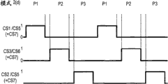
Fig. 8 shows the non-overlapped control signal (CS1-CS6) that is used for control switch (S1-S6) during three states (1,2 and 3) of the main operation embodiment of pattern 1.As mentioned above, this representative is used for an example of many possible cases of control sequence.
Should be appreciated that (sequencing) arranged in the open loop that not necessarily needs to observe above-mentioned three states in proper order.For example, status switch can be: 1,2,3,1,2,3... (as mentioned above); Or 1,3,2,1,3,2...; Or 1,2,1,3,1,2,1,3.Be apparent that also the use of the third state needn't be frequent as other two states, for example it is contemplated that sequence 1,2,1,2,1,2,3,1.Although even it is contemplated that and save the third state fully---only under the well-balanced situation of load, or save alternative for the common mode stabilisation.
Also exist other switches and order to arrange situation.For example, in substituting operational mode 1 embodiment, state 1 can---" state 4 "---be substituted by the 4th state, and switch S 1 and S5 are closed (every other switch is all opened) by this.At this state, capacitor C f charges to input voltage+VDD.The 5th state---" state 5 "---will move in the mode of switch S 2 and S6 closure (every other switch opens) subsequently, so that striding capacitance Cf and the storage capacitance CR1 and CR2 (in this case, the electric capacity of capacitor C R1 and CR2 can the equate) parallel connection that are in series.The specific embodiment that this substituting switch and order are arranged situation has the shortcoming that does not have common mode control, therefore will stand the common mode drift.Yet, change on off sequence by arrange cycle period in " normally " switch and order with proper spacing, this common mode drift of can " resetting ".These changes can be determined in advance, or are activated in response to observed situation.
It should be noted that the big I of capacitor C f, CR1 and CR2 is selected to satisfy desired pulsation tolerance limit (relative with size/cost), therefore, the duration in clock stage of each state needs not to be 1: 1: 1 ratio.
Though above described pattern 1 to generate+/-embodiment of the output of VDD/2, but it will be understood by those skilled in the art that above-mentioned instruction can be used to the quantity by increasing striding capacitance Cf and correspondingly change switching network obtain output into any mark of VDD.In this case, output and the input between relation be Vout+/-=+/-VDD/ (n+1), wherein n equals the quantity of striding capacitance Cf.Also should be understood that the described circuit that has more than a striding capacitance, according to its control, with still can generate+/-output of VDD/2 and between+/-VDD/2 and+/-output of each intermediate integer denominator of correspondence between the VDD/ (n+1).For example, the circuit with two striding capacitances can generate output VDD/3 and VDD/2, and the circuit with three striding capacitances can generate output VDD/4, VDD/3 and VDD/2 etc.
DMCP operation---pattern 2
As mentioned above, DMCP also can the second main pattern---pattern 2---operation, pattern 2 times, DMCP produce double track output+/-VDD (+VDD is the input source voltage level at node N10 place again).Pattern 2 times, switch S 4 is always opened.
The multiple variant of pattern 2 is possible, and these variants will be described below, and is called as pattern 2 (a), 2 (b), 2 (c) and 2 (d).Optional switch S 7 is essential for pattern 2 (c) and 2 (d).
Under pattern 2 (a), described DMCP has two basic running statuses.Fig. 9 a shows with first state in these states--" state 6 "--circuit of operation.Under this state, switch S 1, S2 and S5 are closed (S3, S4 and S6 open).This causes capacitor C f and CR1 to cross over input voltage+VDD and parallel connection between node N10 and N11.Therefore, capacitor C f and CR1 respectively store input voltage+VDD.Fig. 9 b shows the equivalent electric circuit of state 6.
Figure 10 a shows the circuit with second state in these states operation, and this second state is in fact identical with state 2 in the pattern 1, and switch S 3 and S6 are closed (S1, S2, S4 and S5 are opened) by this.Therefore, capacitor C f and CR2 are in parallel between common node N11 and the second output node N13.Therefore, capacitor C f and CR2 share their electric charge, and after a plurality of circulations, and node N13 shows the voltage into-VDD.Figure 10 b shows the equivalent electric circuit of this state 2.
Figure 12 a shows another state, and " state 7 ", it can be introduced into this pattern 2 (a) sequence, and different slightly implementation--this implementation is called as pattern 2 (b) now to create.State 7 times, switch S 1 and S5 are closed (S2, S3, S4 and S6 are opened).This state 7 is in parallel with input voltage+VDD with striding capacitance Cf.Can be state 6 after this state, be state 2 then, gets back to state 7 then, etc.Figure 12 b shows the equivalent electric circuit of this state 7.
Figure 13 shows non-overlapped control signal (CS1-CS3﹠amp; CS5-CS7), it is used for control switch (S1-S3 and S5-S7) to generate the repetitive sequence of above-mentioned three states--7,6,2,7,6,2 etc.., this sequence definition pattern 2 (b).Again, this only represents an example in many possible cases of control sequence.It is to be intended to make CR1 not influenced by CR2 before that state 7 is included in state 6, thereby prevents from intersecting adjustment (cross-regulation).On the other hand, comprise that state 7 has reduced at main state 2 and can be used for time of electric charge transmission for 6 times, thereby, if state 7 is directly omitted (pattern 2 (a)), then adjust and can be enhanced generally.These are design alternatives.
No matter select which kind of mode, the frequent degree that one of described state is used can be not so good as other state (described about pattern 1 as mentioned).For example, if the load on two output node N12, the N13 is unbalanced (for good and all or according to signal conditioning), then comparable another in state 6 and the state 2 is not included more continually, because capacitor C R1 may need not to be recharged more continually than capacitor C R2, otherwise or.
Pattern 2 (c) and (d) be generate+/-the further substituting operational mode of VDD, it is possible when described DMCP is provided with switch S 7.This switch can be used for the combination function of alternative switch S1 and S2, is used for--also namely being connected the load between node N12 and the N11--in high lateral load and does not require that the application of a large amount of electric currents generates positive output voltage at node N12 place.This can be to have under the situation of high input resistance in load, for example has " circuit output (Line Output) " for frequency mixer.Under these circumstances, the size of switch S 7 and driving requirement require to compare with size and the driving of switch S 1 and S2, can be reduced and revise.In fact, run duration switch S 7 under pattern 2 (c) can continue to open, and such advantage is that the required power of driving switch is less, and under the situation of MOS switch implementation, switch S 7 is not because its parasitic grid-leakage and grid-source electric capacity can inject node N10 or N12 with any electric charge.It should be noted that also switch S 1 still need be moved, to generate negative output voltage-VDD.Further, it should be noted that switch S 2 can not operated continually, also striding capacitance Cf and high side storage capacitance CR1 are connected in parallel.
Figure 14 shows non-overlapped control signal (CS1-CS3﹠amp; CS5-CS7), it is used for control switch (S1-S3 and S5-S7) during two alternating states of pattern 2 (c).Therefore, summary pattern 2 (c), switch S 7 by for good and all (or approach for good and all) closure.Amended state 6 is utilized for striding capacitance Cf in parallel and capacitor C R1 charging, and this is by only Closing Switch S1, S5 and S7 realize now.Then, amended state 2 is used to this electric charge is transferred to capacitor C R2 via switch S 3, S6 as before, but this time, because the S7 closure, capacitor C R1 still has the voltage VDD that crosses over its two ends.
Figure 15 shows non-overlapped control signal (CS1-CS3﹠amp; CS5-CS7), it is used for control switch (S1-S3 and S5-S7) during three kinds of states under the variant--it is called as pattern 2 (d)--of pattern 2 (c).Difference between pattern 2 (d) and the pattern 2 (c) is similar to the difference between pattern 2 (a) and 2 (b), is, has inserted an additional stage at state 7 usefulness switches, and wherein switch S 1 and S5 are closed that (S2, S3, S4 and S6 open; S7 can remain closure).Attention mode 2 (d) is followed sequence 7,2,6,7,2,6..., rather than 7,6,2.The effect of these patterns may not have any big-difference, but change sequence freedom can so that control logic simplify, as seeing in the discussion hereinafter.
*If exist
+Pattern 2c and 2d
++Pattern 2d
Table 1
Table 1 shows for above-mentioned seven state of switch (S1-S7) state, the switch that " 0 " expression is opened, and the closed switch of " 1 " expression.Notice that if only use a subclass of described pattern in the specific implementation mode, then switching network and controller do not need to realize whole states 1 to 7.
Again, four exemplary sequence of this of switching network and seven or eight different conditions are not the only possibility of control sequence.Again, according to load, multiple different sequence implementations are possible, and some the frequent degree that are used in these states can be not so good as other states.
Figure 16 shows the DMCP similar with circuit shown in Figure 4 900 circuit, and just DMCP 900 also comprises two comparator 910a, 910b, is used for regulating above-mentioned two output voltages.
It should be noted that DMCP 900 has represented closed loop DMCP.Among comparator 910a, the 910b each is compared its charge pump output voltage (Vout+, Vout-) and corresponding threshold voltage (Vmin+, Vmin-) separately, and exports corresponding charge signal (charge signal) CHCR1 and CHCR2.These charge signals CHCR1, CHCR2 are fed into switch control module 1420, so that switch arrays 1410 are controlled, thereby cause the DMCP operation, with to careless which relevant storage capacitance charging.If at will which output voltage descends above its respective threshold, then start this charge pump; Otherwise make charge pump temporarily out of service.This has reduced the power that consumes in the process of switch switch, especially under underloaded situation.
This scheme allow output voltage be up to+/-VDD/2.Be to be further noted that in this structure, DMCP 900 can be used to generate higher voltage, but be accompanied by the reduction of efficient.In the case, reference voltage (Vmin+/min-) can be conditioned, correspondingly to regulate output voltage.Striding capacitance Cf is charged to+VDD (via switch S 1 and S5), crosses over storage capacitance CR1 (by switch S 2, S5) then or CR2 (by switch S 3, S6) is connected in parallel, and rises to the level of being set by reference voltage with the voltage with them.Such operation has increased the pulsating voltage on storage capacitance CR1, the CR2, but has also reduced switching loss.Yet, by regulating storage capacitance CR1, CR2 with respect to charging capacitor Cf, can reduce pulsating voltage.
Figure 17 shows the double mode charge pump 400 of above-mentioned novelty, another arbitrary embodiment of 900, and wherein in a plurality of different input voltage values can be selected as DMCP 400,900 input voltage.Figure 17 shows the input selector 1000 with a plurality of different voltage inputs (+Vin 1 arrives+Vin N), and selected actual input is definite by control input Ic.Selected voltage level is as double mode charge pump 400,900 input voltage VDD then.
Figure 18 a has represented that a typical case uses, and wherein double track source voltage Vout+ and Vout-are by so as described here charge pump 400,900 generations, and charge pump 400,900 is by for example single track source voltage VDD power supply.Alternatively, charge pump 400,900 can be powered by plurality of source voltages therein, as shown in figure 17.With description that Figure 18 a, 18b are associated in, mark VDD, Vout+ etc. should be interpreted as referring to the voltage at corresponding terminal or this terminal place, based on context decide.
Referring to Figure 18 a, source voltage VDD is illustrated as to treatment circuit 20 power supplies.Input signal S1 can be analog signal or digital signal.Be under the situation of analog signal at S1, treatment circuit 20 will be the pure analogue type circuit, such as operational amplifier, multiplexer, gain module etc.Be that digital signal and output stage are under the situation of simulation at S1, then treatment circuit 20 can be the mixing of digital and analog circuit, wherein signal S1 is by directly or by some Digital Signal Processing feed-in DAC (not shown), and the output of this DAC is fed into above-mentioned analog circuit subsequently.
It is the analog signal that a quilt imports level shifter 30 in this particular for signal S2--who has handled for the treatment of circuit 20 outputs.Level shifter 30 can intercept electric capacity by for example direct current and realize.Output amplifier 40 is by double track source voltage Vout+ and Vout-power supply, and described double track source voltage is generated by charge pump 400,900, and can be in specific embodiments level+/-VDD/2 or+/-VDD, depend on charge pump 400,900 operational mode.Charge pump 400,900 operational mode are determined by control signal Cnl.Pattern 1 can be used for driving low-impedance load such as earphone, exports such as circuit and pattern 2 can be used for driving high impedance load.Model selection can manually be carried out---for example carries out by sound volume setting level (volume setting level) or code, or alternatively, by automatically detecting output impedance or the output current supply is carried out, even under the situation of portable voice frequency equipment, by automatically detecting jack (jack socket) docking station (docking station) operation is carried out.Carry out under the situation of " model selection " in the control of use volume, if volume is set to height and then charge pump is set to pattern 2, to cause the output source voltage collapse under normal conditions because the power demand of load greater than the design charge pump 400,900 at power demand.Yet; the safety device of additional circuit (not shown) form (for example; avoid the damage that the louder volume because of danger causes in order to protect ear) can be placed in suitable position monitoring such situation, with the charge pump 400 of stopping using, 900 or other parts of this circuit.
Analog signal in input signal S1---if simulation---and the treatment circuit 20, usually will be reference with certain voltage between earth potential and the VDD, and the signal S2 ' of level after moving is to be reference approximately, as desired by minute output amplifier of rail source Vout+, Vout-operation.
Signal S2 ' after level moves is fed into output amplifier 40, amplified output signal S3 of amplifier 40 outputs, and what signal S3 was fed into signal transducers 50 forms is (ground referenced) load of reference with ground.Be under the situation of switch (D class or PWM) amplifier or 1 bit digital (sigma-delta) type output stage at output amplifier 40, signal S1, S2 can be digital forms from being input to output always, perhaps can begin is analog form, is converted into digital form then in treatment circuit 20.
Figure 18 b shows the more specifically application of the layout of Figure 18 a: for clarity sake charge pump 400,900 is omitted with powering to be connected.Application among this embodiment is stereo amplifier, and wherein load is stereophone 51.It is two that the Signal Processing Element of this amplifier becomes, handling left channel signal and right-hand signal, as the suffix ' L ' in their reference symbol and ' R ' shown in.Source voltage Vout+ and Vout-can be by these two Channel Sharing, although if should application need, it also is possible being used for the independently-powered of different channels.An application is portable voice frequency equipment such as MP 3 players, for example wherein divides the rail source to allow DC-coupling output---it is desirablely needn't use big decoupling capacitor to keep bass response.
Figure 19 a and 19b show the mancarried electronic aid that uses in two kinds of layouts, by this, for every kind of layout, arbitrary all can being advantageously used to provides power with proper level to output stage in the above-mentioned DMCP embodiment.
Figure 19 a shows the portable electronic audio frequency equipment 1 in first layout, and it is connected to drive a pair of earphone 2.Equipment 1 in the diagram is the MP3 player, but identical functions can be integrated among phone, multimedia player, kneetop computer, PDA and the like.Earphone 2 is connected to this equipment via the lead-in wire 3 that is inserted into output plughole (jack) 4.The main body of this equipment also can comprise one or more Microspeaker (not shown), and described Microspeaker can be driven as substituting audio frequency output transducer, but is equal to the earphone for illustration purpose on the principle.As everyone knows, small size and weight and long battery life are the crucial qualities of quality product on the market.Production cost is the key factor on the whole market.
Figure 19 b shows the identical device 1 in second layout, does not wherein connect earphone.This equipment changes into via independent connector and is connected to docking station 5, and docking station 5 drives bigger loud speaker 6L, 6R again.Docking station 5 comprises than portable unit self having more high-power amplifier, and independent power supply---it is mains supply normally.Figure 19 c shows the identical device in second variant of arranging, wherein replaces earphone, and external amplifier 7 and loud speaker 8L, 8R are connected via circuit lead-in wire (the line lead) 9 that is inserted into earphone jack 4.
Equipment 1 is required the load that driving stage is inequality in these different layouts.Earphone or loud speaker have 32 ohm or littler impedance usually.Go deep into this load, for example the output amplitude of 100mV RMS for the volume that calls the turn corresponding to the full scale of 30mW power etc. (for example-12dB) will provide.When drive second arrange in during the circuit input of big amplifier, normally 10 kilo-ohms or bigger of described load impedances, thus the full scale signal amplitude (0dB) of 2V RMS for best in quality be suitable.If the output stage of driven socket (socket) can provide the signal of 2V RMS in first arranges, then its source voltage must be greater than 2V.When the earphone load from identical output stage drive arrangement 1, the major part of described output stage power consumption all dissipates with the form of heat, because source voltage can drop to the level of 100mV in the transistor of output stage.If in order to increase battery life, the designer selects not provide full 2V RMS for circuit output situation, the result is worse signal so.
Because these conflicting needs, quality product on the market conventionally adopts the way that the output stage of separating mutually is provided, an output stage is used for driving earpiece/speaker load 2, and another output stage is used for circuit output situation via dock connector (docking connector) 4.Each output stage all can be driven by the power supply that is suitable for described voltage range, thereby keeps power-efficient and quality in each is used.There is no need to go into details, to the output stage of separating mutually and the demand that is used for their power supply that separates mutually, do not conform to size and cost that people's will ground has increased equipment.
Described DMCP can be included into such equipment 1, thereby has exempted the demand to the output stage of separating mutually.Can change into single output stage is provided, DMCP is as its power supply.In this embodiment, when this equipment was driving earphone load, DMCP can be arranged to pattern 1 operation; And when this equipment drove another amplifier by circuit output, DMCP can be arranged to pattern 2 operations.
Ideally, described DMCP is automatically moved with appropriate mode according to apparatus arrangement.Be used to second at the dock connector that separates with earphone jack 4 and arrange under the situation of (Figure 19 b), which kind of pattern the control circuit of described DMCP can---it indicates inserting state (docked status)---direct decision should use according to overall signal.When identical jack 4 as be used in first be used in arranging second arrange in the time, can select with several mode deterministic models.As first option, switch or the menu option that can have the user to use are to make clear and definite selection between sound and circuit output mode.Alternatively, volume control is being transferred in the action of full scale, the user sets and can imply, and can not be used in the basis that is assumed to be under the max volume with earphone in practice.Alternatively, might even under the situation of portable audio device, detect jack docking station is operated, carry out by automatically detecting output impedance or output current supply.
Other the possible application that needs to generate the ability of dividing the rail source comprises: (1) wherein is that the DC-coupling output signal of reference can be avoided black level decline (black-level droop) with ground for the treatment of the voltage source of the circuit of analog composite video signal; And the line driver that (2) are used for data link or modulator-demodulator wherein is that the DC-coupling output signal of reference can weaken baseline shift effect (baseline wander effect) with ground such as ADSL.
For the reason of cost and size, it is very important the function of MP 3 players, mobile phone or other application arbitrarily can being integrated in a small amount of integrated circuit.---to be charge pump 400,900 in the case---be integrated together with functional circuit 20,30,40 etc. the circuit that therefore will be used for the generation of source voltage is favourable.Generally speaking, charge pump 400,900 comprises and can not be integrated practically and must be positioned at capacitor outside the sheet, therefore integrated circuit chip number of pins and overall circuit size has been brought influence.Because many circuit requirements have ambipolar source (dividing the rail source), this has promoted using single capacitor---rather than for capacitor of each required output voltage use---to generate the development of the voltage generation circuit of two (or more) output voltage sources.
Control scheme, controller form and even many other modifications of the details aspect of switching network be changeable.Having the reader of technology to understand, is possible to above-mentioned and other modification and the increase of these circuit, and do not break away from as defined by the appended claims, the spirit and scope of the present invention.Therefore, to propose above-mentioned embodiment and be in order to illustrate, rather than in order to limit the scope of the invention.In order to explain this specification and claim, the reader should notice that word " comprises " element do not got rid of except the element of listing in the claims or step or the existence of step, singular article " one " or " one " do not get rid of plural number (unless context has requirement in addition), and discrete component also can be realized the function of a plurality of elements described in the claim.Any reference marker all should not be understood that the scope of claim is limited in the claim.
Claim statement element " be connected " or the situation of " being used for connecting " under, this should not be interpreted as requiring to get rid of the direct connection of any other element, and should be interpreted as being enough to connection that those elements can be worked as described.There is the reader of technology to understand; design good, practicality may comprise many NM execution herein for example startup and closing function, measuring ability, error protection or suchlike accessory; in these accessories some are mentioned, and neither one impairs in each embodiment of the invention described above and the basic function characteristic of the present invention in the claim in these accessories.
In above-mentioned whole description, mark Vout+, Vout-and VDD etc. should be interpreted as referring to the voltage at corresponding terminal or this terminal place, based on context decide.
Except the variation in the charge pump circuit self and modification, equipment and the system of described charge pump that the present invention has also comprised including in of form of ownership also has the Earphone Amplifier shown in Figure 15 to use.The power supply of this circuit can be used for the equipment of form of ownership---comprising communication equipment---output stage, but wherein output stage driven antenna or transmission line, electrical-optical transducer (luminescent device) or electromechanical transducer.