Embodiment
1. represent embodiment at first, the summary of the representative embodiment of invention disclosed among the application is described.Represent in the summary description of embodiment, the reference marks of enclosing the drawing of parantheses reference only is the part that the concept of its appended inscape of example comprises.
(1) the related control method for nonvolatile memory of representative embodiment of the present invention, comprise nonvolatile memory (14), can generate random number randomizer (12) but and be combined with above-mentioned randomizer and the system of the controller (15) of the above-mentioned nonvolatile memory of access in implement.That is, during at every turn to above-mentioned nonvolatile memory access, make above-mentioned controller determine to refresh target area according to the random number that above-mentioned randomizer occurs, carry out the refresh control that this district is write again.
According to such control method, determine to refresh target area according to the random number that above-mentioned randomizer occurs, can be to each the access object district (Page1~PageN) refresh equably in the nonvolatile memory to writing again of this district.Refresh by this, can make the threshold value of storage unit return the front state of change.In addition, random number occuring during at every turn to above-mentioned nonvolatile memory access, the access object district corresponding with this random number write again, therefore, can avoid causing writing indegree and increasing undesirably because refreshing.
(2) aggregate value of the access times in the whole access objects district of management in the above-mentioned nonvolatile memory and refresh target area, when each access to above-mentioned nonvolatile memory occurs, make above-mentioned controller renewal to the aggregate value of the access times of above-mentioned nonvolatile memory, upgrade the result according to this, carry out and refresh the refresh control that target area writes again to above-mentioned.Thereby, can be to the access object district (Page1~PageN) refresh equably in the nonvolatile memory.Refresh by this, can make the threshold value of storage unit return the front state of change.
(3) in above-mentioned (2), the refresh control of above-mentioned controller can comprise: when each access to above-mentioned nonvolatile memory occurs, obtain the whole access objects district in the above-mentioned nonvolatile memory access times aggregate value the 1st process (602,1001); The 2nd of the aggregate value that more above-mentioned the 1st processing obtains and the threshold value of regulation processed (603,1004); According to the above-mentioned the 2nd comparative result of processing, the above-mentioned target area that refreshes is carried out the 3rd processing (605,1006) that writes again; And after the above-mentioned the 3rd processes, upgrade as required the 4th of above-mentioned threshold value and process (607,1009).
(4) in above-mentioned (2), the refresh control of above-mentioned controller can comprise: when each access to above-mentioned nonvolatile memory occurs, obtain the aggregate value of access times in the whole access objects district in the above-mentioned nonvolatile memory and each access object district access times difference the 5th process (1202,1404); The 6th of the difference that more above-mentioned the 5th processing obtains and the threshold value of regulation processed (1203,1405); Process the difference of obtaining according to the above-mentioned the 6th and determine to refresh target area, this is refreshed target area carry out the 7th processing (1204,1406) that writes again that refreshes usefulness.
(5) in above-mentioned (2), the refresh control of above-mentioned controller can comprise: when the access of above-mentioned nonvolatile memory being occured at every turn, obtain the aggregate value of access times in the whole access objects district in the above-mentioned nonvolatile memory and each the access object district in the above-mentioned nonvolatile memory access times difference the 8th process (1804); Obtain the above-mentioned the 8th and process the 9th processing (1806) in corresponding the 1st access object district of difference less than the threshold value of regulation in the difference that obtains.Then, can comprise: differentiate between the 1st access object district that above-mentioned the 9th processing obtains and the 2nd access object district that is different from it, could process (1807) with the 10th of physical address replacement logic address; In the above-mentioned the 10th differentiation of processing, judge the occasion of replacement logic address, available physical address, between above-mentioned the 1st access object district and above-mentioned the 2nd access object district, process (1808) with the 11st of physical address replacement logic address.And, can comprise: in the above-mentioned the 10th differentiation of processing, judge the occasion of unavailable physical address replacement logic address, process the difference of obtaining according to the above-mentioned the 8th and determine to refresh target area, this is refreshed target area carry out the 12nd processing (1810) that writes again that refreshes usefulness.
(6) in above-mentioned (5), above-mentioned the 2nd access object district can process the difference that obtains according to the above-mentioned the 8th and determine.
(7) the related semiconductor device (10) of representative embodiment of the present invention comprises nonvolatile memory (14).Then, setting can generate the randomizer (12) of random number and determine to refresh target area according to the random number of above-mentioned randomizer generation at every turn to above-mentioned nonvolatile memory access the time, carries out the controller (15) of the refresh control that this district is write again.
(8) the related semiconductor device (10) of representative embodiment of the present invention comprises nonvolatile memory (14).Then, setting can manage the whole access objects district in the above-mentioned nonvolatile memory access times aggregate value and refresh the directorial area (51) of target area and when the access of above-mentioned nonvolatile memory being occured, upgrade aggregate value to the access times of above-mentioned nonvolatile memory at every turn, according to this renewals result execution to the above-mentioned controller (15) that refreshes the refresh control that target area writes again.
(9) in above-mentioned (8), above-mentioned directorial area can form with the part of the storage area in the above-mentioned nonvolatile memory.
(10) in above-mentioned (8), above-mentioned directorial area can form in the semiconductor memory that independently arranges with above-mentioned nonvolatile memory.
(11) in above-mentioned (8), above-mentioned controller is carried out: when the access of above-mentioned nonvolatile memory being occured at every turn, obtain the whole access objects district in the above-mentioned nonvolatile memory access times aggregate value the 1st process (602,1001); The 2nd of the aggregate value that more above-mentioned the 1st processing obtains and the threshold value of regulation processed (603,1004); According to the above-mentioned the 2nd comparative result of processing, the above-mentioned target area that refreshes is carried out the 3rd processing (605,1006) that writes again; After above-mentioned the 3rd processing, upgrade as required the 4th of above-mentioned threshold value and process (607,1009).
(12) in above-mentioned (8), above-mentioned controller is carried out: when each access to above-mentioned nonvolatile memory occurs, obtain the aggregate value of access times in the whole access objects district in the above-mentioned nonvolatile memory and each access object district access times difference the 5th process (1202,1404); The 6th of the difference that more above-mentioned the 5th processing obtains and the threshold value of regulation processed (1203,1405); Process the difference of obtaining according to the above-mentioned the 6th and determine to refresh target area, this is refreshed target area carry out the 7th processing (1204,1406) that writes again that refreshes usefulness.
(13) in above-mentioned (8), above-mentioned semiconductor device also comprises the logical/physical address mapping table (17) that is transformed into the physical address of above-mentioned nonvolatile memory for the logical address that will give from the outside.Then, above-mentioned controller is carried out: when the access of above-mentioned nonvolatile memory being occured at every turn, obtain the aggregate value of access times in the whole access objects district in the above-mentioned nonvolatile memory and each the access object district in the nonvolatile memory access times difference the 8th process (1804); Obtain the above-mentioned the 8th and process the 9th processing (1806) in corresponding the 1st access object district of above-mentioned difference less than the threshold value of regulation in the difference that obtains.And above-mentioned controller is carried out: to differentiate between the 1st access object district that above-mentioned the 9th processing obtains and the 2nd access object district different from it, could process (1807) with the 10th of physical address replacement logic address; In the above-mentioned the 10th differentiation of processing, judge the occasion of replacement logic address, available physical address, between above-mentioned the 1st access object district and above-mentioned the 2nd access object district, process (1808) with the 11st of physical address replacement logic address.Then, above-mentioned controller is carried out: in the above-mentioned the 10th differentiation of processing, judge the occasion of unavailable physical address replacement logic address, process the difference of obtaining according to the above-mentioned the 8th and determine to refresh target area, this is refreshed target area carry out the 12nd processing (1810) that writes again that refreshes usefulness.
(14) above-mentioned access object district, by the above-mentioned nonvolatile memory of sector unit's access the time, be made as " sector ", by the above-mentioned nonvolatile memory of page unit access the time, be made as " page ", by the above-mentioned nonvolatile memory of block unit access the time, be made as " piece ".In addition, above-mentioned access comprises access that above-mentioned nonvolatile memory is write, the access that above-mentioned nonvolatile memory is deleted and the access of reading from above-mentioned nonvolatile memory.
2. the embodiment explanation then is described in more detail embodiment.
<embodiment 1〉Fig. 1 represents the configuration example as the microcomputer of a routine semiconductor device of the present invention.Microcomputer 10 shown in Figure 1 is not particularly limited, but comprise processor 11, randomizer 12, program storage 13, nonvolatile memory 14 and access controller 15, adopt known SIC (semiconductor integrated circuit) manufacturing technology to form in the Semiconductor substrate of monocrystalline substrate etc.Processor 11, randomizer 12, program storage 13 and nonvolatile memory 14 connect via bus 9, can mutually exchange various signals.Nonvolatile memory 14 for example is Single MONOS (the Metal Oxide Nitride OxideSemiconductor) storer that is made of 1 bit 1 transistor.
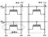
Above-mentioned nonvolatile memory 14 is arranged by a plurality of array of non-volatile memory cells shapes and is formed the various data of using in the stores processor in the above-mentioned processor 11.Nonvolatile memory 14 consists of by a plurality of, and as shown in Figure 2, each piece is made of a plurality of page Page1~PageN.Write, delete or read all and carry out take this page as unit.In deletion, the operation bias voltage that applies regulation in each pattern such as write or read.For example, shown in Figure 20 A, apply-8.5V at Memory-Gate (MG) during deletion, apply supply voltage 1.5V in well region, source electrode (S) and drain electrode (D), by tunnel effect the electronics in the nitride film is extracted into the well region side, thereby the threshold value (Vth) of storage unit is located at minus side.Shown in Figure 20 B, write and fashionablely apply 1.5V at Memory-Gate MG, apply-10.5V in well region, source electrode (S) and drain electrode (D), in nitride film, inject electronics by tunnel effect, thereby the threshold value (Vth) of storage unit is located at positive side.Shown in Figure 20 C, apply 0V at the MG that selects when reading, source electrode (S) is set as 0V, and will drain (D) is set as 1.0V, thereby, if storage unit is the deletion state, then because Vth for negative, detects current flowing between drain electrode (D)-source electrode (S), drain potential descends, if storage unit is write state, then because that Vth for just, detects between drain electrode (D)-source electrode (S) not current flowing, drain potential remains in 1V is constant.In addition, shown in Figure 20 D, when keeping (standby), apply voltage-1.5V below the storage unit deletion Vth at MG, well region.
By the assigned voltage shown in Figure 20 A-Figure 20 D being applied in Memory-Gate MG, well region, source electrode (S) and the drain electrode (D), can deleting, write and read the position of selecting.In addition, in this case, in order to prevent the misoperation of unselected position (the non-position of selecting), need to apply prevention voltage in non-selection position.But owing to applying of above-mentioned prevention voltage, the non-position of selecting becomes weak deletion state or write state when deleting, writing and reading, thereby the threshold value (Vth) that storage unit occurs changes, and namely disturbs.As the countermeasure for interference, consideration refreshes by writing when writing at every turn or reading or deleting again, but, suppose when writing at every turn or reading or deleting, to refresh, what have each page writes indegree because of this refresh activity but not the anxiety of increase desirably.Thereby, refresh as follows in this example.
True random numbers occur in above-mentioned randomizer 12, on the number that namely occurs without the random number of bias.Above-mentioned processor 11 program is according to the rules implemented the calculation process of regulation.In addition, above-mentioned processor 11 is administered the operation control of whole microcomputer 10.The refresh control of above-mentioned nonvolatile memory 14 in this example, by enforcements such as above-mentioned processor 11 or above-mentioned access controllers 15, but hypothesis is implemented by access controller 15 in this explanation.In the refresh control that above-mentioned access controller 15 is implemented, above-mentioned nonvolatile memory 14 is write fashionablely at every turn, determine to refresh the object page based on the random number that above-mentioned randomizer 12 occurs, and this page is write again.
Here, the maximal value of the random number that above-mentioned randomizer 12 generates is made as the abundant large value than the total page number N in the above-mentioned nonvolatile memory 14.The purpose of doing like this is, judges in this routine refresh control whether the value of the random number that occurs is comprised by 1~N, if the value of random number is comprised by 1~N, just implements to write for refreshing again.If the maximal value of the random number that above-mentioned randomizer 12 generates is set as than the little value of total page number N in the above-mentioned nonvolatile memory 14, all will implement to write for refreshing when then random number occuring again at every turn, the result can implement above the refreshing of desired times.
Preserve the program that above-mentioned processor 11 is implemented in the said procedure storer 13.
Fig. 3 represents the flow process of refresh control.
Processor 11 writes to the data of access controller 15 requests to a certain page, for example PageM, access controller 15 writes PageM (301) with data, also make random number generator 12 that random number X (302) occurs, and whether the value of the random number X of differentiation generation is comprised (303) by 1~N thereupon.In this is differentiated, comprised (YES) if be judged as the value of the random number of generation by 1~N, access controller 15 just writes and implements to refresh the page corresponding with this random number (PageX).The value of the random number that for example occurs is " 3 ", just Page3 is refreshed.Like this, according to this example, each during data writing, by random number generator 12 true random numbers occur, and the page corresponding with this true random number write again on a certain page of nonvolatile memory 14.Here, true random number does not have bias at the number that occurs, therefore can be without (the Page1~PageN) of each page in the bias ground refresh of non-volatile memory 14.Because this refreshes, the threshold value of storage unit returns to the front state of change.Also have, if nonvolatile memory 14 consists of by a plurality of, and each piece also (Page1~PageN) consist of then utilizes the refresh control of processor 11 too as above in other pieces by a plurality of pages.
Example on the foundation can obtain following effect.
During (1) at every turn to a certain page data writing of nonvolatile memory 14, true random number occurs by random number generator 12, and the page corresponding with this true random number write again, therefore, can be without (the Page1~PageN) of each page in the bias ground refresh of non-volatile memory 14.Refresh by this, the threshold value of storage unit returns to the front state of change.
(2) by the action effect of above-mentioned (1), can seek the reliability of microcomputer 10 and improve.
(3) if when writing or reading or deleting, nonvolatile memory 14 is refreshed at every turn, what then have each page writes indegree because this refresh activity but not the anxiety of increase desirably, but, as described above, each on a certain page of nonvolatile memory 14 during data writing, by random number generator 12 true random number occuring, the page corresponding with this true random number write again, just can avoid writing indegree because refreshing but not desirably increase.
<embodiment 2〉Fig. 4 represents to be made as another configuration example of the microcomputer of a routine semiconductor device of the present invention.Microcomputer shown in Figure 4 10 is with main difference point shown in Figure 1, and randomizer 12 is omitted, but replaces the directorial area that refreshes of guaranteeing in nonvolatile memory 14.In this example, access controller 15 carries out refresh control based on the management information in the above-mentioned directorial area.For example shown in Figure 5, above-mentioned nonvolatile memory 14 is established directorial area 51 in addition outside Page1~PageN.In this directorial area 51, set about the aggregate value of writing indegree (being called " always writing indegree ") of whole pages of nonvolatile memory 14 and be made as the information of the page (refreshing the page) that refreshes object in order to appointment.Each information in this directorial area 51 is upgraded by access controller 15.
Fig. 6 represents the main-process stream of the refresh control in the microcomputer shown in Figure 4 10.Have, this refresh control is by enforcements such as processor 11 or access controllers 15 again, and hypothesis is implemented by access controller 15 in this explanation.In addition, Fig. 7 represents the state variation of the nonvolatile memory 14 in the above-mentioned refresh control.Have again, among Fig. 7, the additional shadow line be the page that is written into, with underscore is the page that is refreshed.
If the state of Fig. 7 (A) is original state.Under this original state, always write indegree and be made as " 0 ", refresh the page and be made as " Page1 ".In addition, threshold X is set as " 10000 ".Consider that now the control by access controller 15 is carried out the situation that data write to above-mentioned nonvolatile memory 14 under this state.By the control of access controller 15, for example write (601) in the enterprising row data of the Page2 of above-mentioned nonvolatile memory 14.This writes an end, just by processor 11 with reference to directorial area 51, that obtains nonvolatile memory 14 always writes indegree (602).Then, in processor 11, always write the whether differentiation (603) larger than threshold X of indegree.Threshold X is set in processor 11 interior suitable registers etc.In the differentiation of step 603, always write indegree and be not more than threshold X (NO) if be judged as, then will always write indegree by the control of access controller 15 and upgrade (609).For example, under the original state of Fig. 7 (A), always write indegree and be " 0 ", this value is not more than threshold X, therefore is judged as " NO " in the differentiation of step 603, always writes indegree and is updated (609).In the example shown in Fig. 7 (B), always write indegree and be updated to " 1 " from " 0 ".Similarly, under the state shown in Fig. 7 (C), carry out the data of Page300 are write.Always write indegree this moment becomes " 9999 ".Under the state shown in Fig. 7 (D), carry out the data of Page150 are write.Always write indegree this moment becomes " 10000 ".Under the state shown in Fig. 7 (E), carry out the data of Page511 are write.Always write indegree this moment becomes " 10001 ", has surpassed threshold X at this moment=10000.Under this state, in the differentiation of step 603, be judged as " YES ".In the differentiation of above-mentioned steps 603, if be judged as " YES ", just obtain the information (604) that refreshes the page from directorial area 51.Then, whether need the differentiation (605) that refreshes.For example, if in above-mentioned steps 601, the page that refreshes of obtaining in the above-mentioned steps 604 has been done to write, this is refreshed the page write again for refreshing with regard to not needing.Thereby, in above-mentioned steps 605, the page of having done to write in the page and the above-mentioned steps 601 that refreshes of obtaining in the above-mentioned steps 604 is compared, if the same page, just being judged as does not need this page furbishing (NO), if the different pages, just being judged as need to be to this page furbishing (YES).In the differentiation of above-mentioned steps 605, need to refresh (YES) if be judged as, just the page (being Page1 here) with correspondence refreshes, and namely implements to write (606) again.Then, according to carrying out the differentiation (607) whether needs upgrade threshold X with the relation of always writing indegree.In addition, in the differentiation of above-mentioned steps 605, do not need (NO) to refresh if be judged as, just do not carry out refreshing in the above-mentioned steps 606, and carry out the differentiation of above-mentioned steps 607.
Surpass threshold X if always write indegree, then in the differentiation of step 607, be judged as " YES ", accordingly threshold X has been updated to the value (608) greater than so far value.Here, if the value of threshold X is not changed to value greater than so far value, then a certain page is being write fashionablely at every turn, in the differentiation of step 603, must be judged as " YES " and implement to refresh, will carry out continually unnecessary writing again.For fear of this situation, when always writing indegree and surpassed threshold X, in the differentiation of step 606, be judged as " YES ", and thus threshold X be updated to the large value (608) of value than so far.So, after threshold X is updated, refreshes the page and be updated (609), then, always write indegree and be updated (610).When need not to upgrade threshold X owing to the relation of always writing indegree, in the differentiation of above-mentioned steps 607, be judged as " NO ", threshold X is not updated, and is updated (609) and refresh the page, afterwards, always writes indegree and is updated (610).In the example shown in Fig. 7 (E), always write indegree and be made as " 10001 ", refresh the page and be updated to " Page2 ", therefore, carrying out the data of Page511 are write fashionable, in the differentiation of step 603, be judged as " YES ", in step 605, carrying out refreshing of Page2.
Example on the foundation can obtain following action effect.
(1) at every turn with a certain page of data write non-volatile memory 14 time, always write indegree whether greater than the differentiation (603) of threshold value, if always write indegree greater than threshold value, just refresh as refreshing the page that the page is obtained.So, since with the relation of always writing indegree, threshold X is updated (609).By such refresh control, can be without (the Page1~PageN) of each page in the bias ground refresh of non-volatile memory 14.And refresh by this, the threshold value of storage unit is restored to state before the change.
(2) because the effect of above-mentioned (1) can be sought the reliability improvement of microcomputer 10.
(3) in nonvolatile memory 14, suppose when writing at every turn or reading or deleting and refresh, what just have each page writes indegree because of this refresh activity but not the anxiety of increase desirably, but as described above, at each indegree of always writing during data writing on to a certain page of nonvolatile memory 14 whether greater than the differentiation (603) of threshold value, when always writing indegree greater than threshold value, will as the page furbishing that refreshes the page and obtain, therefore can avoid writing indegree because of refreshing but not desirably increase.
<embodiment 3〉Fig. 8 represents to be made as another configuration example of the microcomputer of a routine semiconductor device of the present invention.Microcomputer 10 shown in Figure 8 is with main difference point shown in Figure 4, guarantees to refresh directorial area in each page in nonvolatile memory 14 and externally forms and refresh directorial area 16.The above-mentioned directorial area 16 that refreshes is formed on RAM (random access memory) of being connected in bus 9 etc.For example shown in Fig. 9 (A), above-mentioned nonvolatile memory 14 arranges directorial area at each page.Shown in Fig. 9 (B), this directorial area comprises the memory block of refreshing sign and always writing indegree.Here, refreshing sign is to indicate whether to have made the sign that refreshes, for example refreshes tag logic value for " 0 " expression also refreshes, and refreshes tag logic value and refreshes complete for " 1 " expression.Refresh directorial area 16 and be when being kept at power connection by what the searching, managing district obtained and always write indegree and refresh the zone of the page.Utilize this to refresh directorial area 16, the time that retrieval is always write indegree and refreshed the page in the time of can saving each access memory.
Figure 10 represents the main-process stream of the refresh control in the microcomputer shown in Figure 8 10.Have, this refresh control is by enforcements such as processor 11 or access controllers 15 again, but hypothesis is implemented by access controller 15 in this explanation.In addition, Figure 11 represents the state variation of the nonvolatile memory 14 in the above-mentioned refresh control.Have again, among Figure 11, the additional shadow line be the page that is written into, with underscore is the page that is refreshed.
The state of Figure 11 (A) is made as original state.In this original state, all the pages (for example among the Page1~Page511), refresh sign and are set as logical value " 0 ", always write indegree and be set as " 0 ".In addition, threshold X is set as " 10000 ".
At first, access controller 15 is always write indegree (1001) with reference to what refresh that directorial area 16 obtains nonvolatile memory 14.Then, by the control of access controller 15, write (1002) in the enterprising row data of a certain page of nonvolatile memory 14, the directorial area of this page is also upgraded (1003) immediately.Then, always write the differentiation (1004) whether indegree reaches threshold X.In this is differentiated, always write indegree and do not reach threshold X (NO), then end process if be judged as.For example, shown in Figure 11 (B), during data writing, the directorial area of this Page2 also is updated on Page2.In the example shown in Figure 11 (B), do not carry out writing beyond the Page2, so " 0 " of indegree to this time of always writing of nonvolatile memory 14 is updated to " 1 ".In addition, in the example shown in Figure 11 (C), write in the enterprising row data of Page300, at this moment, the data of having carried out other pages write, and the indegree of always writing of nonvolatile memory 14 is updated to " 9999 ".And, in the example shown in Figure 11 (D), write in the enterprising row data of Page150, write by the data to this Page150, the indegree of always writing of nonvolatile memory 14 becomes " 10000 ", reaches threshold X at this moment=10000, therefore, in the differentiation of step 1004, be judged as " YES ", obtain and refresh the page (1005).Then, whether need the differentiation (1006) that refreshes.For example, if in above-mentioned steps 1001, done to refresh writing of the page to what obtain in the above-mentioned steps 1004, this is refreshed the page write again for refreshing with regard to not needing.In above-mentioned steps 1006, the page that refreshes of obtaining in the above-mentioned steps 1005 is compared with the page of having done to write in above-mentioned steps 1001, if the same page, just be judged as refresh (NO) that does not need to carry out to this page, if the different pages, just being judged as needs (YES) to carry out refreshing this page.In the differentiation of above-mentioned steps 1006, need (YES) to refresh if be judged as, just implement corresponding refreshing namely of the page (being Page1) here and write again (1007).Have again, refresh sign during with reference to power connection in the directorial area, this is refreshed the page that is masked as logical value " 0 " refreshing directorial area 16 as refreshing Page-saving.If a plurality of pages that refresh are arranged, then select the page that refreshes of page number minimum wherein.Then, refresh the renewal of directorial area 16 and be refreshed the renewal (1008) of the directorial area of the page.For example, in the example shown in Figure 11 (D), carry out refreshing of Page1, the corresponding logical value " 0 " of sign to this time that refresh is updated to logical value " 1 " therewith.In addition, in the example shown in Figure 11 (E), write by the data to Page511, the indegree of always writing of nonvolatile memory 14 becomes " 10001 ", threshold X at this moment=10000 have been reached, therefore, in the differentiation of step 1004, be judged as " YES ", obtain and refresh the page (1005).In this example, the sign that refreshes about Page1 is made as logical value " 1 ", therefore refresh and finish, carry out refresh (1007) to Page2, corresponding with this Page2 logical value " 0 " of sign to this time that refresh is updated to logical value " 1 " (1008).Like this, the data of at every turn carrying out a certain page are write fashionable, always write the differentiation (1004) whether indegree reaches threshold X, and refresh (1007) based on this differentiation result.Then, whether need to upgrade the differentiation (1008) of threshold X.If the refresh all sign corresponding with Page1~Page511 becomes logical value " 1 ", then being judged as needs to upgrade threshold X (YES), " 10000 " of threshold X to this time are updated to such as (1010) such as " 30000 ", and directorial area returns to original state.Then, again begin refresh control shown in Figure 10.
Example on the foundation can obtain following action effect.
(1) writes fashionablely in the data of carrying out a certain page at every turn, always write the differentiation (1004) whether indegree reaches threshold X, and refresh (1007) based on this differentiation result.Then, whether need to upgrade the differentiation (1009) of threshold X.When the refresh all sign corresponding with Page1~Page511 became logical value " 1 ", threshold X was updated.By such refresh control, can be without (the Page1~PageN) of each page in the bias ground refresh of non-volatile memory 14.And, refreshing by this, the threshold value of storage unit returns to the front state of change.
(2) according to the action effect of above-mentioned (1), can seek the reliability of microcomputer 10 and improve.
(3) in nonvolatile memory 14, refresh if be arranged in when writing or reading or deleting at every turn, what then have each page writes indegree because of this refresh activity but not the anxiety of increase desirably, but, owing to always writing as described above the differentiation (1004) whether indegree reaches threshold X, and refreshing (1007) based on this differentiation result, the unexpected increase of writing indegree that refreshes that therefore results from is avoided.
<embodiment 4〉main-process stream of another refresh control in Figure 12 presentation graphs 4 and the structure shown in Figure 5.
In directorial area shown in Figure 5 51, the work of always writing indegree and each page of storage non-volatile memories 14 write the fashionable indegree of always writing, implement refresh control by processor 11 or access controller 15 etc. based on this value.Have, hypothesis is implemented by access controller 15 in this explanation again.In addition, Figure 13 represents the state variation of the nonvolatile memory 14 in the above-mentioned refresh control.Have again, among Figure 13, the additional shadow line be the page that is written into, with underscore is the page that is refreshed.
The state of Figure 13 (A) is made as original state.In this original state, always to write indegree and be " 0 ", the indegree of writing of each page is made as " 0 ".In addition, threshold X is located at " 4000 ".Consider now under this state to carry out the situation that the data to above-mentioned nonvolatile memory 14 write by the control of access controller 15.
At first, write (1201) in the enterprising row data of a certain page, access controller 15 is with reference to directorial area 51 shown in Figure 5, obtain each page work write and fashionable always write indegree and always write difference (1202) between the indegree.For example shown in Figure 13 (B), made data at Page150 and write fashionable (1201), write indegree about the data of this Page150 and be " 1 ", write indegree about the data of other pages and be " 0 ", at this moment, the indegree of always writing of nonvolatile memory 14 becomes " 1 ".
Then, differentiate each page work write the fashionable difference of always writing indegree and always writing between the indegree and whether reach threshold X (1203).In this is differentiated, do not reach threshold X (NO) if be judged as difference, then done always writing indegree, always writing indegree and be updated (1206) of the page that writes.In addition, in the differentiation of step 1203, reached threshold X (YES) if be judged as difference, then with the page furbishing (1204) of difference maximum in the difference of obtaining.In the example shown in Figure 13 (C), the indegree of always writing of Page1 is " 5000 ", the indegree of always writing of Page2 is " 1000 ", the indegree of always writing of Page150 is " 3340 ", the indegree of always writing of Page300 is " 2300 ", the indegree of always writing of Page511 is " 4300 ", and the indegree of always writing of nonvolatile memory 14 is " 5000 ".The indegree of always writing of Page2 is " 1000 ", the difference of always writing between the indegree " 5000 " of it and nonvolatile memory 14 becomes " 4000 ", this difference has reached threshold X=4000, therefore be judged as YES in the differentiation of step 1004, the page of difference maximum (being Page2 here) is refreshed (1204).Why like this, be because the page of difference maximum writes least number of times, have precedence over other pages to anti-interference.Then, shown in Figure 13 (D), made the page that writes and the writing indegree, always write indegree and be updated (1205) of the page having done to refresh.
Example on the foundation can obtain following action effect.
(1) each on a certain page of nonvolatile memory 14 during data writing, obtain writing indegree and always writing difference (1202) between the indegree of each page, whether the difference of writing indegree and always writing between the indegree of differentiating each page reaches threshold X (1203), in the differentiation of step 1203, when being judged as difference and having reached threshold X (YES), page furbishing (1204) with difference maximum in the difference of obtaining, thereby, can be without (the Page1~Page511) of each page in the bias ground refresh of non-volatile memory 14.And, refreshing by this, the threshold value of storage unit returns to the front state of change.
(2) because the effect of above-mentioned (1) can be sought the reliability improvement of microcomputer 10.
(3) in nonvolatile memory 14, refresh if be arranged in when writing or reading or deleting at every turn, what then have each page writes indegree because of this refresh activity but not the anxiety of increase desirably, but, obtain writing indegree and always writing difference between the indegree of each page, and when judging that this difference has reached threshold X (YES) with the difference of obtaining in the page furbishing of difference maximum, thereby avoid writing indegree because of refreshing but not desirably increase.
<embodiment 5〉main-process stream of another refresh control in Figure 14 presentation graphs 8 and the structure shown in Figure 9.In the directorial area of each page, store each page work write the fashionable indegree of always writing.In addition, shown in Figure 8 refreshing have searching, managing district when power connection in the directorial area 16 and obtain always write indegree, and implement refresh control based on this by processor 11 or access controller 15.Have, hypothesis is implemented by access controller 15 in this explanation again.In addition, Figure 15 represents the state variation of the directorial area in the above-mentioned refresh control.Have, the additional shadow line is to have made the page that writes among Figure 15 again, and with underscore is to have made the page that refreshes.
The state of Figure 15 (A) is made as original state.In this original state, always to write indegree and be made as " 0 ", the indegree of writing of each page is made as " 0 ".In addition, threshold X is set in " 4000 ".Consider now by the control of processor 11 above-mentioned nonvolatile memory 14 to be carried out the situation that data write at this state.
At first, with reference to refreshing directorial area 16, that obtains nonvolatile memory 14 always writes indegree (1401) by access controller 15.Then, made data at a certain page and write fashionable (1402), the directorial area of this page also is updated (1403).Namely, have in the directorial area of each page what this page had been done moment that data write and always write indegree.In addition, also will refresh the indegree of always writing of storing in the directorial area 16 upgrades.Then, always write difference (1404) between the indegree by what access controller 15 was obtained the retention value of directorial area of each page and current time.Then, differentiate the difference of obtaining in the above-mentioned steps 1404 and whether reached threshold X (1405).In the differentiation of step 1405, do not reach threshold X (NO) if be judged as the difference of obtaining in the above-mentioned steps 1404, with regard to end process.In the differentiation of step 1405, reached threshold X (YES) if be judged as the difference of obtaining in the above-mentioned steps 1404, the page of the difference maximum of then obtaining in the above-mentioned steps 1404 is refreshed (1406), and refresh the page directorial area be updated (1407).In addition, refreshing the indegree of always writing of storing in the directorial area 16 also is updated.For example, among Figure 15 (B), write by the data of enforcement to Page150, the indegree of always writing of directorial area is updated to " 1 ".In the example shown in Figure 15 (C), the directorial area corresponding with Page1 becomes " 5000 ", because this value is maximum, the current indegree of always writing of nonvolatile memory 14 is represented as " 5000 ".Then, make data at Page300 and write fashionable, corresponding with this Page300 directorial area, shown in Figure 15 (D), be updated to 5000+1=5001 (1403).In addition, under the state of Figure 15 (C), that obtains the retention value of directorial area of each page and current time always writes difference (1404) between the indegree, the difference of always writing between the indegree (5000) of the retention value of the directorial area of Page2 (1000) and current time is " 4000 ", this value has reached threshold X=4000, the page of the difference maximum of obtaining (being Page2 here) is refreshed (1406), and the directorial area of this page is updated to " 5001 ".
Example on the foundation can obtain following effect.
(1) write (1402) if made data at a certain page, the indegree of always writing of having done in the directorial area of this page that writes just is updated (1403).Then, by access controller 15, that obtains the retention value of directorial area of each page and current time always writes difference (1404) between the indegree, and whether the difference of carrying out afterwards obtaining in the above-mentioned steps 1404 reaches the differentiation (1405) of threshold X.In the differentiation of step 1405, if be judged as YES, the page of the difference maximum of then obtaining in the above-mentioned steps 1404 is refreshed (1406), and refresh the page directorial area be updated (1407).Thereby, can be without (the Page1~Page511) of each page in the bias ground refresh of non-volatile memory 14.And because this refreshes, the threshold value of storage unit returns to the front state of change.
(2) by the action effect of above-mentioned (1), can seek the reliability of microcomputer 10 and improve.
(3) in the nonvolatile memory 14, refresh if be arranged in when writing or reading or deleting at every turn, what just have each page writes indegree because of this refresh activity but not the anxiety of increase desirably, but just can avoid in the following way writing indegree because refreshing but not desirably increase: always write difference (1404) between the indegree at the retention value of the directorial area of obtaining each page and current time, and when being judged as this difference and having reached threshold X (YES), with the page furbishing of difference maximum in the difference of obtaining.
<embodiment 6〉Figure 16 represents to be made as another configuration example of the microcomputer of a routine semiconductor device of the present invention.Microcomputer 10 shown in Figure 16 is with the main difference point of microcomputer shown in Figure 8, is provided with the logical/physical address mapping table 17 that is transformed to the physical address in the nonvolatile memory 14 in order to the logical address that processor 11 is given.When access controller 15 accessing non-volatile memory 14, logical address is transformed into the physical address of nonvolatile memory 14 by logical/physical address mapping table 17, carry out writing or reading etc. nonvolatile memory 14 with this physical address.For example shown in Figure 17 (A), above-mentioned nonvolatile memory 14 is established directorial area at each page.Shown in Figure 17 (B), this directorial area comprises the conversion sign and always writes the memory block of indegree.Here, the conversion sign represents to carry out the replacement of the physical address corresponding with logical address, and for example the conversion sign represents when " 0 " replaceablely in logical value, and conversion represents not replaceable when being masked as logical value " 1 ".The zone of always writing indegree of refreshing directorial area 16 and being searching, managing district when being stored in power connection and obtain.Refresh directorial area 16 by this, the time of indegree is always write in retrieval in the time of can saving each access memory.
Figure 18 represents the main-process stream of the refresh control in the microcomputer shown in Figure 16 10.This refresh control is implemented by processor 11 or access controller 15, and hypothesis is implemented by access controller 15 in this explanation.In addition, Figure 19 represents the state variation of the directorial area in the above-mentioned refresh control.Have again, among Figure 19, the additional shadow line be the page that is written into, with underscore is the page that is refreshed.
The state of Figure 19 (A) is made as original state.In this original state, all (for example the conversion sign among the Page1~Page511) is set in logical value " 0 " to the pages, always writes indegree and is set in " 0 ".In addition, threshold X is set in " 4000 ".Under this state, obtained by access controller 15 and always to write indegree (1801).Then, one carries out data and writes (1802) on a certain page, and the directorial area of this page just is updated (1803).In addition, the indegree of always writing that refreshes directorial area 16 also is updated.For example shown in Figure 19 (B), write fashionablely having made data by access controller 15 at Page150, access controller 15 is updated to " 1 " with " 0 " of indegree to this time of always writing of the directorial area of Page150.Then, obtain each page directorial area value with always write the difference (1804) of indegree, and carry out the differentiation (1805) whether this difference reaches threshold X.For example in the example shown in Figure 19 (C), the value of the directorial area of Page2 is made as " 1000 ", and this value and the difference " 4000 " of always writing between the indegree " 5000 " of this moment have reached threshold X (being set as 4000 here).Thereby, in the differentiation of step 1805, be judged as YES, specifically, obtain the difference obtained in the above-mentioned steps 1804 less than the page (1806) of threshold value Y.Here threshold value Y is made as the value less than threshold X, such as " 100 " etc., is set in the suitable register in the processor 11 etc.Then, the state (1807) of the conversion sign of the page obtained of examination.If the state of conversion sign is logical value " 0 ", represent replaceablely, therefore between the page of the difference maximum of obtaining and difference are less than the page of threshold value Y, carry out page replacement (1808), the directorial area of each page also is updated (1809).For example in the example shown in Figure 19 (D), and the page of always writing the difference maximum between the indegree (5001) is Page2, and difference is Page1 less than the page of threshold value Y.And the state of their conversion sign is logical value " 0 ", therefore carries out the replacement (1808) between Page1 and the Page2 here.The replacement of this page by Page1 physical address and the replacement between the physical address of Page2 realize.After Page1 and Page2 had done to replace, the directorial area of each page was updated (1809).In addition, in the differentiation of above-mentioned steps 1807, if be judged as not replaceable (NO), just with the page furbishing (1810) of difference maximum, and the directorial area of the refreshing page upgraded (1811).For example in the example shown in Figure 19 (E), carry out the refreshing of Page2 of difference maximum, the maximum of its directorial area is write indegree and is updated to " 5001 ".
Example on the foundation can obtain following effect.
(1) write fashionable having made data by access controller 15, obtain the value and the difference (1804) of always writing indegree of the directorial area of each page, carry out the differentiation (1805) whether this difference reaches threshold X, the page of difference maximum is refreshed (1810), refresh the page directorial area also be updated (1811).Thereby, can be without (the Page1~Page511) of each page in the bias ground refresh of non-volatile memory 14.And, refreshing by this, the threshold value of storage unit returns to the front state of change.
(2) carry out page replacement capable (1808) between the page of the difference maximum of obtaining and difference are less than the page of threshold value Y, the directorial area of each page is upgraded (1809).This page replacement is realized by the physical address of replacement Page1 and the physical address of Page2.Thereby (bias of writing indegree among the Page1~Page511) is further reduced each page in the nonvolatile memory 14.
(3) by the effect of above-mentioned (1), (2), can seek the reliability of microcomputer 10 and improve.
(4) in nonvolatile memory 14, refresh if be arranged in when writing or reading or deleting at every turn, what each page was then arranged writes indegree because of this refresh activity but not the anxiety of increase desirably, but, the situation of writing in the following way indegree because refreshing but not desirably increasing is avoided: that obtains the retention value of directorial area of each page and current time always writes difference (1804) between the indegree, when being judged as this difference and having reached threshold X, with the page furbishing of difference maximum in the difference of obtaining.
Above, done to specifically describe with regard to the invention that the inventor finishes, but the present invention is not limited by this, the present invention can have various distortion in the scope that does not depart from its main idea.
For example, implement refresh control by access controller 15 in the upper example, still, also can outside above-mentioned processor 11, access controller 15, establish in addition the controller of this refresh control special use.
In the upper example, write fashionable to above-mentioned nonvolatile memory at every turn, the random number that perhaps occurs based on randomizer determines to refresh the object page, perhaps upgrade the aggregate value (always writing indegree) of writing indegree, but, also can when carrying out the deletion of above-mentioned nonvolatile memory at every turn or reading, determine to refresh the object page based on the random number that randomizer occurs, and upgrade the aggregate value of deletion number of times or read-around number.
In the upper example, be arranged to carry out refresh control with the indegree of writing of nonvolatile memory, but, also can replace the indegree of writing about whole pages of nonvolatile memory, and use deletion number of times or read-around number about whole pages of nonvolatile memory to carry out refresh control.
In the upper example, the access object district is made as the page (Page), but not limited by this.For example, also the access object district can be made as sector or piece.
In addition, always writing indegree can be recorded among the RAM (random access memory) in the microcomputer 10.If above-mentioned RAM does not have the reinforcement of battery etc., before then can facing at the power supply of system interruption the indegree of always writing in the above-mentioned RAM is kept out of the way in the suitable nonvolatile memory, and when system power-on reset, the indegree of always writing in the above-mentioned nonvolatile memory is written into above-mentioned RAM.
In the above explanation, main just the invention of finishing take the inventor as the application of background be that applicable cases in the microcomputer is described, but the present invention is not limited by this, can be widely used in semiconductor device.