CN101872130B - Lithographic projection apparatus - Google Patents
Lithographic projection apparatus Download PDFInfo
- Publication number
- CN101872130B CN101872130B CN2010101140186A CN201010114018A CN101872130B CN 101872130 B CN101872130 B CN 101872130B CN 2010101140186 A CN2010101140186 A CN 2010101140186A CN 201010114018 A CN201010114018 A CN 201010114018A CN 101872130 B CN101872130 B CN 101872130B
- Authority
- CN
- China
- Prior art keywords
- liquid
- substrate
- projection
- immersion liquid
- space
- Prior art date
- Legal status (The legal status is an assumption and is not a legal conclusion. Google has not performed a legal analysis and makes no representation as to the accuracy of the status listed.)
- Expired - Fee Related
Links
- 239000007788 liquid Substances 0.000 claims abstract description 184
- 238000007654 immersion Methods 0.000 claims abstract description 99
- 239000000758 substrate Substances 0.000 claims abstract description 64
- 230000005855 radiation Effects 0.000 claims abstract description 40
- 238000007789 sealing Methods 0.000 claims abstract description 12
- 239000000203 mixture Substances 0.000 claims abstract description 11
- 239000007789 gas Substances 0.000 claims description 17
- 238000000059 patterning Methods 0.000 claims description 17
- 239000012530 fluid Substances 0.000 claims description 10
- 238000005259 measurement Methods 0.000 claims description 10
- 230000007246 mechanism Effects 0.000 claims description 10
- QVGXLLKOCUKJST-UHFFFAOYSA-N atomic oxygen Chemical compound [O] QVGXLLKOCUKJST-UHFFFAOYSA-N 0.000 claims description 9
- 239000001301 oxygen Substances 0.000 claims description 9
- 229910052760 oxygen Inorganic materials 0.000 claims description 9
- 238000010276 construction Methods 0.000 claims description 8
- 238000002604 ultrasonography Methods 0.000 claims description 6
- 238000000746 purification Methods 0.000 claims description 5
- 239000012528 membrane Substances 0.000 claims description 3
- 238000011144 upstream manufacturing Methods 0.000 abstract description 4
- XLYOFNOQVPJJNP-UHFFFAOYSA-N water Substances O XLYOFNOQVPJJNP-UHFFFAOYSA-N 0.000 description 38
- VYPSYNLAJGMNEJ-UHFFFAOYSA-N Silicium dioxide Chemical compound O=[Si]=O VYPSYNLAJGMNEJ-UHFFFAOYSA-N 0.000 description 14
- 239000002245 particle Substances 0.000 description 12
- 238000000034 method Methods 0.000 description 11
- 239000000463 material Substances 0.000 description 10
- 238000012545 processing Methods 0.000 description 8
- 239000000126 substance Substances 0.000 description 8
- 230000003287 optical effect Effects 0.000 description 7
- 239000000377 silicon dioxide Substances 0.000 description 7
- 230000001351 cycling effect Effects 0.000 description 6
- 238000004821 distillation Methods 0.000 description 6
- 239000010410 layer Substances 0.000 description 6
- 150000002894 organic compounds Chemical class 0.000 description 6
- 230000003252 repetitive effect Effects 0.000 description 6
- 238000003860 storage Methods 0.000 description 6
- 241000195493 Cryptophyta Species 0.000 description 5
- 229930195733 hydrocarbon Natural products 0.000 description 5
- 150000002430 hydrocarbons Chemical class 0.000 description 5
- 239000013043 chemical agent Substances 0.000 description 4
- 230000000694 effects Effects 0.000 description 4
- 238000005516 engineering process Methods 0.000 description 4
- 238000004519 manufacturing process Methods 0.000 description 4
- 239000008399 tap water Substances 0.000 description 4
- 235000020679 tap water Nutrition 0.000 description 4
- XUIMIQQOPSSXEZ-UHFFFAOYSA-N Silicon Chemical compound [Si] XUIMIQQOPSSXEZ-UHFFFAOYSA-N 0.000 description 3
- 239000002671 adjuvant Substances 0.000 description 3
- 230000008901 benefit Effects 0.000 description 3
- 230000005540 biological transmission Effects 0.000 description 3
- 230000004087 circulation Effects 0.000 description 3
- 238000013461 design Methods 0.000 description 3
- 239000010408 film Substances 0.000 description 3
- 238000002955 isolation Methods 0.000 description 3
- 230000008569 process Effects 0.000 description 3
- 229910052710 silicon Inorganic materials 0.000 description 3
- 239000010703 silicon Substances 0.000 description 3
- 239000000243 solution Substances 0.000 description 3
- CURLTUGMZLYLDI-UHFFFAOYSA-N Carbon dioxide Chemical compound O=C=O CURLTUGMZLYLDI-UHFFFAOYSA-N 0.000 description 2
- 239000006172 buffering agent Substances 0.000 description 2
- 230000008859 change Effects 0.000 description 2
- 150000001875 compounds Chemical class 0.000 description 2
- 238000011109 contamination Methods 0.000 description 2
- 238000002242 deionisation method Methods 0.000 description 2
- 238000005115 demineralization Methods 0.000 description 2
- 230000002328 demineralizing effect Effects 0.000 description 2
- 239000000284 extract Substances 0.000 description 2
- 238000011049 filling Methods 0.000 description 2
- 238000003384 imaging method Methods 0.000 description 2
- 238000005342 ion exchange Methods 0.000 description 2
- 210000003205 muscle Anatomy 0.000 description 2
- 230000010363 phase shift Effects 0.000 description 2
- 238000001259 photo etching Methods 0.000 description 2
- 230000029553 photosynthesis Effects 0.000 description 2
- 238000010672 photosynthesis Methods 0.000 description 2
- 230000001105 regulatory effect Effects 0.000 description 2
- 238000001223 reverse osmosis Methods 0.000 description 2
- 230000035939 shock Effects 0.000 description 2
- 239000000080 wetting agent Substances 0.000 description 2
- 241000894006 Bacteria Species 0.000 description 1
- WKBOTKDWSSQWDR-UHFFFAOYSA-N Bromine atom Chemical compound [Br] WKBOTKDWSSQWDR-UHFFFAOYSA-N 0.000 description 1
- OKTJSMMVPCPJKN-UHFFFAOYSA-N Carbon Chemical compound [C] OKTJSMMVPCPJKN-UHFFFAOYSA-N 0.000 description 1
- 239000004215 Carbon black (E152) Substances 0.000 description 1
- ZAMOUSCENKQFHK-UHFFFAOYSA-N Chlorine atom Chemical compound [Cl] ZAMOUSCENKQFHK-UHFFFAOYSA-N 0.000 description 1
- LFQSCWFLJHTTHZ-UHFFFAOYSA-N Ethanol Chemical compound CCO LFQSCWFLJHTTHZ-UHFFFAOYSA-N 0.000 description 1
- 241000233866 Fungi Species 0.000 description 1
- CBENFWSGALASAD-UHFFFAOYSA-N Ozone Chemical compound [O-][O+]=O CBENFWSGALASAD-UHFFFAOYSA-N 0.000 description 1
- 241001464837 Viridiplantae Species 0.000 description 1
- IKHGUXGNUITLKF-XPULMUKRSA-N acetaldehyde Chemical compound [14CH]([14CH3])=O IKHGUXGNUITLKF-XPULMUKRSA-N 0.000 description 1
- 238000013459 approach Methods 0.000 description 1
- 239000007864 aqueous solution Substances 0.000 description 1
- 239000002585 base Substances 0.000 description 1
- GDTBXPJZTBHREO-UHFFFAOYSA-N bromine Substances BrBr GDTBXPJZTBHREO-UHFFFAOYSA-N 0.000 description 1
- 229910052794 bromium Inorganic materials 0.000 description 1
- 239000000872 buffer Substances 0.000 description 1
- 229910052799 carbon Inorganic materials 0.000 description 1
- 229910002092 carbon dioxide Inorganic materials 0.000 description 1
- 239000001569 carbon dioxide Substances 0.000 description 1
- 239000003610 charcoal Substances 0.000 description 1
- 229910052801 chlorine Inorganic materials 0.000 description 1
- 239000000460 chlorine Substances 0.000 description 1
- 238000004140 cleaning Methods 0.000 description 1
- 239000002131 composite material Substances 0.000 description 1
- 230000001276 controlling effect Effects 0.000 description 1
- 238000005520 cutting process Methods 0.000 description 1
- 238000007872 degassing Methods 0.000 description 1
- 238000007033 dehydrochlorination reaction Methods 0.000 description 1
- 238000000151 deposition Methods 0.000 description 1
- 230000008021 deposition Effects 0.000 description 1
- 239000006185 dispersion Substances 0.000 description 1
- 238000009826 distribution Methods 0.000 description 1
- 230000005670 electromagnetic radiation Effects 0.000 description 1
- 238000005530 etching Methods 0.000 description 1
- 230000002349 favourable effect Effects 0.000 description 1
- 238000001914 filtration Methods 0.000 description 1
- 230000003760 hair shine Effects 0.000 description 1
- 229910052736 halogen Inorganic materials 0.000 description 1
- 150000002367 halogens Chemical class 0.000 description 1
- 229910001385 heavy metal Inorganic materials 0.000 description 1
- 239000001307 helium Substances 0.000 description 1
- 229910052734 helium Inorganic materials 0.000 description 1
- SWQJXJOGLNCZEY-UHFFFAOYSA-N helium atom Chemical compound [He] SWQJXJOGLNCZEY-UHFFFAOYSA-N 0.000 description 1
- 238000004128 high performance liquid chromatography Methods 0.000 description 1
- 230000006872 improvement Effects 0.000 description 1
- 239000012535 impurity Substances 0.000 description 1
- 238000009434 installation Methods 0.000 description 1
- 150000002500 ions Chemical class 0.000 description 1
- 239000002346 layers by function Substances 0.000 description 1
- 230000004807 localization Effects 0.000 description 1
- 238000003754 machining Methods 0.000 description 1
- 230000005381 magnetic domain Effects 0.000 description 1
- 238000012423 maintenance Methods 0.000 description 1
- 239000011159 matrix material Substances 0.000 description 1
- QSHDDOUJBYECFT-UHFFFAOYSA-N mercury Chemical compound [Hg] QSHDDOUJBYECFT-UHFFFAOYSA-N 0.000 description 1
- 229910052753 mercury Inorganic materials 0.000 description 1
- 238000001465 metallisation Methods 0.000 description 1
- 238000004377 microelectronic Methods 0.000 description 1
- 230000003647 oxidation Effects 0.000 description 1
- 238000007254 oxidation reaction Methods 0.000 description 1
- 230000003071 parasitic effect Effects 0.000 description 1
- 238000005498 polishing Methods 0.000 description 1
- 238000002360 preparation method Methods 0.000 description 1
- 238000007639 printing Methods 0.000 description 1
- 238000005086 pumping Methods 0.000 description 1
- 238000005070 sampling Methods 0.000 description 1
- 239000013049 sediment Substances 0.000 description 1
- 239000004065 semiconductor Substances 0.000 description 1
- 238000000926 separation method Methods 0.000 description 1
- 238000007493 shaping process Methods 0.000 description 1
- 241000894007 species Species 0.000 description 1
- 229910001220 stainless steel Inorganic materials 0.000 description 1
- 239000010935 stainless steel Substances 0.000 description 1
- 239000004094 surface-active agent Substances 0.000 description 1
- 230000001360 synchronised effect Effects 0.000 description 1
- 239000010409 thin film Substances 0.000 description 1
- 238000012546 transfer Methods 0.000 description 1
- 238000009281 ultraviolet germicidal irradiation Methods 0.000 description 1
- 239000002351 wastewater Substances 0.000 description 1
Images


Classifications
-
- G—PHYSICS
- G03—PHOTOGRAPHY; CINEMATOGRAPHY; ANALOGOUS TECHNIQUES USING WAVES OTHER THAN OPTICAL WAVES; ELECTROGRAPHY; HOLOGRAPHY
- G03F—PHOTOMECHANICAL PRODUCTION OF TEXTURED OR PATTERNED SURFACES, e.g. FOR PRINTING, FOR PROCESSING OF SEMICONDUCTOR DEVICES; MATERIALS THEREFOR; ORIGINALS THEREFOR; APPARATUS SPECIALLY ADAPTED THEREFOR
- G03F7/00—Photomechanical, e.g. photolithographic, production of textured or patterned surfaces, e.g. printing surfaces; Materials therefor, e.g. comprising photoresists; Apparatus specially adapted therefor
- G03F7/20—Exposure; Apparatus therefor
-
- G—PHYSICS
- G03—PHOTOGRAPHY; CINEMATOGRAPHY; ANALOGOUS TECHNIQUES USING WAVES OTHER THAN OPTICAL WAVES; ELECTROGRAPHY; HOLOGRAPHY
- G03F—PHOTOMECHANICAL PRODUCTION OF TEXTURED OR PATTERNED SURFACES, e.g. FOR PRINTING, FOR PROCESSING OF SEMICONDUCTOR DEVICES; MATERIALS THEREFOR; ORIGINALS THEREFOR; APPARATUS SPECIALLY ADAPTED THEREFOR
- G03F7/00—Photomechanical, e.g. photolithographic, production of textured or patterned surfaces, e.g. printing surfaces; Materials therefor, e.g. comprising photoresists; Apparatus specially adapted therefor
- G03F7/70—Microphotolithographic exposure; Apparatus therefor
- G03F7/708—Construction of apparatus, e.g. environment aspects, hygiene aspects or materials
- G03F7/70858—Environment aspects, e.g. pressure of beam-path gas, temperature
- G03F7/70866—Environment aspects, e.g. pressure of beam-path gas, temperature of mask or workpiece
-
- B—PERFORMING OPERATIONS; TRANSPORTING
- B01—PHYSICAL OR CHEMICAL PROCESSES OR APPARATUS IN GENERAL
- B01D—SEPARATION
- B01D61/00—Processes of separation using semi-permeable membranes, e.g. dialysis, osmosis or ultrafiltration; Apparatus, accessories or auxiliary operations specially adapted therefor
- B01D61/02—Reverse osmosis; Hyperfiltration ; Nanofiltration
- B01D61/025—Reverse osmosis; Hyperfiltration
-
- B—PERFORMING OPERATIONS; TRANSPORTING
- B01—PHYSICAL OR CHEMICAL PROCESSES OR APPARATUS IN GENERAL
- B01D—SEPARATION
- B01D19/00—Degasification of liquids
- B01D19/0031—Degasification of liquids by filtration
-
- B—PERFORMING OPERATIONS; TRANSPORTING
- B01—PHYSICAL OR CHEMICAL PROCESSES OR APPARATUS IN GENERAL
- B01D—SEPARATION
- B01D61/00—Processes of separation using semi-permeable membranes, e.g. dialysis, osmosis or ultrafiltration; Apparatus, accessories or auxiliary operations specially adapted therefor
- B01D61/24—Dialysis ; Membrane extraction
-
- C—CHEMISTRY; METALLURGY
- C02—TREATMENT OF WATER, WASTE WATER, SEWAGE, OR SLUDGE
- C02F—TREATMENT OF WATER, WASTE WATER, SEWAGE, OR SLUDGE
- C02F1/00—Treatment of water, waste water, or sewage
- C02F1/20—Treatment of water, waste water, or sewage by degassing, i.e. liberation of dissolved gases
-
- G—PHYSICS
- G03—PHOTOGRAPHY; CINEMATOGRAPHY; ANALOGOUS TECHNIQUES USING WAVES OTHER THAN OPTICAL WAVES; ELECTROGRAPHY; HOLOGRAPHY
- G03F—PHOTOMECHANICAL PRODUCTION OF TEXTURED OR PATTERNED SURFACES, e.g. FOR PRINTING, FOR PROCESSING OF SEMICONDUCTOR DEVICES; MATERIALS THEREFOR; ORIGINALS THEREFOR; APPARATUS SPECIALLY ADAPTED THEREFOR
- G03F7/00—Photomechanical, e.g. photolithographic, production of textured or patterned surfaces, e.g. printing surfaces; Materials therefor, e.g. comprising photoresists; Apparatus specially adapted therefor
- G03F7/70—Microphotolithographic exposure; Apparatus therefor
- G03F7/70216—Mask projection systems
- G03F7/70341—Details of immersion lithography aspects, e.g. exposure media or control of immersion liquid supply
-
- C—CHEMISTRY; METALLURGY
- C02—TREATMENT OF WATER, WASTE WATER, SEWAGE, OR SLUDGE
- C02F—TREATMENT OF WATER, WASTE WATER, SEWAGE, OR SLUDGE
- C02F1/00—Treatment of water, waste water, or sewage
- C02F1/02—Treatment of water, waste water, or sewage by heating
- C02F1/04—Treatment of water, waste water, or sewage by heating by distillation or evaporation
-
- C—CHEMISTRY; METALLURGY
- C02—TREATMENT OF WATER, WASTE WATER, SEWAGE, OR SLUDGE
- C02F—TREATMENT OF WATER, WASTE WATER, SEWAGE, OR SLUDGE
- C02F1/00—Treatment of water, waste water, or sewage
- C02F1/28—Treatment of water, waste water, or sewage by sorption
-
- C—CHEMISTRY; METALLURGY
- C02—TREATMENT OF WATER, WASTE WATER, SEWAGE, OR SLUDGE
- C02F—TREATMENT OF WATER, WASTE WATER, SEWAGE, OR SLUDGE
- C02F1/00—Treatment of water, waste water, or sewage
- C02F1/28—Treatment of water, waste water, or sewage by sorption
- C02F1/283—Treatment of water, waste water, or sewage by sorption using coal, charred products, or inorganic mixtures containing them
-
- C—CHEMISTRY; METALLURGY
- C02—TREATMENT OF WATER, WASTE WATER, SEWAGE, OR SLUDGE
- C02F—TREATMENT OF WATER, WASTE WATER, SEWAGE, OR SLUDGE
- C02F1/00—Treatment of water, waste water, or sewage
- C02F1/30—Treatment of water, waste water, or sewage by irradiation
- C02F1/32—Treatment of water, waste water, or sewage by irradiation with ultraviolet light
-
- C—CHEMISTRY; METALLURGY
- C02—TREATMENT OF WATER, WASTE WATER, SEWAGE, OR SLUDGE
- C02F—TREATMENT OF WATER, WASTE WATER, SEWAGE, OR SLUDGE
- C02F1/00—Treatment of water, waste water, or sewage
- C02F1/42—Treatment of water, waste water, or sewage by ion-exchange
-
- C—CHEMISTRY; METALLURGY
- C02—TREATMENT OF WATER, WASTE WATER, SEWAGE, OR SLUDGE
- C02F—TREATMENT OF WATER, WASTE WATER, SEWAGE, OR SLUDGE
- C02F1/00—Treatment of water, waste water, or sewage
- C02F1/44—Treatment of water, waste water, or sewage by dialysis, osmosis or reverse osmosis
- C02F1/441—Treatment of water, waste water, or sewage by dialysis, osmosis or reverse osmosis by reverse osmosis
-
- C—CHEMISTRY; METALLURGY
- C02—TREATMENT OF WATER, WASTE WATER, SEWAGE, OR SLUDGE
- C02F—TREATMENT OF WATER, WASTE WATER, SEWAGE, OR SLUDGE
- C02F2103/00—Nature of the water, waste water, sewage or sludge to be treated
- C02F2103/34—Nature of the water, waste water, sewage or sludge to be treated from industrial activities not provided for in groups C02F2103/12 - C02F2103/32
- C02F2103/40—Nature of the water, waste water, sewage or sludge to be treated from industrial activities not provided for in groups C02F2103/12 - C02F2103/32 from the manufacture or use of photosensitive materials
-
- G—PHYSICS
- G03—PHOTOGRAPHY; CINEMATOGRAPHY; ANALOGOUS TECHNIQUES USING WAVES OTHER THAN OPTICAL WAVES; ELECTROGRAPHY; HOLOGRAPHY
- G03F—PHOTOMECHANICAL PRODUCTION OF TEXTURED OR PATTERNED SURFACES, e.g. FOR PRINTING, FOR PROCESSING OF SEMICONDUCTOR DEVICES; MATERIALS THEREFOR; ORIGINALS THEREFOR; APPARATUS SPECIALLY ADAPTED THEREFOR
- G03F7/00—Photomechanical, e.g. photolithographic, production of textured or patterned surfaces, e.g. printing surfaces; Materials therefor, e.g. comprising photoresists; Apparatus specially adapted therefor
- G03F7/20—Exposure; Apparatus therefor
- G03F7/2041—Exposure; Apparatus therefor in the presence of a fluid, e.g. immersion; using fluid cooling means
Landscapes
- Chemical & Material Sciences (AREA)
- Engineering & Computer Science (AREA)
- Water Supply & Treatment (AREA)
- Chemical Kinetics & Catalysis (AREA)
- Physics & Mathematics (AREA)
- General Physics & Mathematics (AREA)
- Health & Medical Sciences (AREA)
- Nanotechnology (AREA)
- Life Sciences & Earth Sciences (AREA)
- Environmental & Geological Engineering (AREA)
- Urology & Nephrology (AREA)
- Atmospheric Sciences (AREA)
- Epidemiology (AREA)
- Public Health (AREA)
- Toxicology (AREA)
- Organic Chemistry (AREA)
- Hydrology & Water Resources (AREA)
- Exposure And Positioning Against Photoresist Photosensitive Materials (AREA)
- Exposure Of Semiconductors, Excluding Electron Or Ion Beam Exposure (AREA)
Abstract
A lithographic projection apparatus comprises a radiation system for providing radiation projection light beam; a supporting structure for supporting a composition apparatus, wherein the composition apparatus can perform the composition on the projection light beam according to required patterns; a substrate platform for holding the substrate; a projection system for projecting the radiation light beam with the pattern onto a target part of the substrate; and a liquid supply system with immersion liquid to at least partly fill the space between the last element of the projection system and the substrate. The liquid supply system comprises a liquid purifier for purifying the immersion liquid. The liquid purifier comprises a gas removing unit which is positioned at upstream of the space and is not contacted with the space. A non-contact sealing is formed around the projection lens of the projection system through the liquid supply system, so that the immersion liquid at least partly fills the space between the main surface of the substrate facing the projection system and the final element of the projection system.
Description
The application is the applicant in the denomination of invention of application on August 27th, 2004 is dividing an application of 200410068266.6 application for a patent for invention for " lithographic equipment and device making method ", application number.
Technical field
The present invention relates to a kind of lithographic projection apparatus, comprising: the illuminator that is used to provide the radiation projecting beam; Be used to support the supporting construction of patterning apparatus, said patterning apparatus is used for according to required pattern projecting beam being carried out composition; Be used to keep the base station of substrate; Be used for patterned light beam is projected the projection system on the target part of substrate.And be used for the last element of the partially filled at least said projection system of immersion liquid and the liquid-supplying system in the space between the said substrate.
Background technology
Term used herein " patterning apparatus " should broadly be interpreted as gives the device in patterned cross section can for the radiation laser beam of incident, and wherein said pattern is consistent with the pattern that will on the target part of substrate, form; " light valve " also uses a technical term among this paper.Usually, the particular functional layer corresponding (like hereinafter) of said pattern and the device that in target part, forms such as integrated circuit or other device.The example of this patterning apparatus comprises:
Mask.The notion of mask is known in photoetching.It comprises the mask-type like binary type, alternating phase-shift type and attenuating phase-shift type, and various hybrid mask types.The layout of this mask in radiation laser beam makes the radiation incided on the mask can be according to the pattern on the mask and optionally by transmission (under the situation of transmission mask) or be reflected (under the situation of reflection mask).Under the situation of using mask, supporting construction generally is a mask platform, and it can guarantee that mask is maintained at the desired location in the incident beam, and this can move relative to light beam if desired.
Array of programmable mirrors.An example of this equipment is the matrix-addressable surface with a viscoelasticity key-course and a reflecting surface.The ultimate principle of this device is that the addressed areas of (for example) reflecting surface reflects incident light as diffraction light, and addressed areas does not reflect incident light as non-diffracted light.With a suitable light filter, the said non-diffracted light of filtering only keeps diffraction light from beam reflected; In this manner, light beam produces pattern according to the addressing pattern of matrix-addressable surface.Another embodiment of array of programmable mirrors utilizes the arranged of tiny mirror, through using suitable internal field, perhaps through using piezoelectric actuator device, makes that each catoptron can be independently about the material that inclines.Moreover catoptron is a matrix-addressable, thus addressed mirrors with the radiation laser beam reflection of direction that addressed mirrors is not different with incident; In this manner, the addressing pattern according to the matrix-addressable catoptron carries out composition to folded light beam.Can carry out this required matrix addressing with suitable electronic installation.In above-mentioned two kinds of situation, patterning apparatus can comprise one or more array of programmable mirrors.The more information of reflection mirror array can obtain from for example U.S. Pat 5,296,891, U.S. Pat 5,523,193, PCT patented claim WO 98/38597 and WO 98/33096, and these documents are here introduced as reference.In the situation of array of programmable mirrors, said supporting construction can be framework or worktable, for example said structure can be as required fix or movably.
■ Programmable LCD array, for example by U.S. Pat 5,229, the 872 this structures that provide, it is here introduced as reference.As stated, supporting construction can be framework or worktable in this case, for example said structure can be as required fix or movably.
For the sake of simplicity, the remainder of this paper is an example with mask and mask platform specifically under certain situation; , the General Principle of in such example, being discussed should be applicable to the patterning apparatus of above-mentioned more wide region.
Lithographic projection apparatus can be used for the for example manufacturing of integrated circuit (IC).In this case, patterning apparatus can produce the circuit pattern corresponding to an individual course of IC, and the target that this pattern can be imaged on the substrate (silicon wafer) that has applied radiation-sensitive materials (resist) layer partly goes up (for example comprising one or more tube core (die)).General, single wafer will comprise the whole grid of adjacent target part, and this adjacent target part is by projection system radiation in succession one by one.Adopting the mask on the mask platform to carry out in the device of composition at present, two kinds of dissimilar machines are arranged.One type of lithographic projection apparatus is, through with whole mask pattern single exposures on the target part and each target part of radiation; The so-called wafer stepper of this device.Another kind of device (so-called stepping-scanister) is through given reference direction (" scanning " direction) scans mask pattern successively in the projecting beam lower edge, also each target part of radiation is come with the parallel or antiparallel direction synchronous scanning of this direction base station in the edge simultaneously; Because in general, projection system has a magnification M (usually<1), and therefore the scan velocity V to base station is M times to mask bench scanning speed.About as the more information of lithographic equipment described herein can be from for example obtaining in the U.S. Pat 6,046,792, the document is introduced here as a reference.
In the manufacturing approach with lithographic projection apparatus, (for example in mask) pattern is imaged in the substrate that part at least covers by one deck radiation-sensitive materials (resist).Before this image-forming step, can carry out various processing to substrate, like bottoming, apply resist and weak baking.After exposure, can carry out other processing to substrate, like postexposure bake (PEB), develop, toast by force and measure/check imaging features.Be the basis with this series of process, the individual layer of the device of for example IC is formed pattern.This patterned layer can be carried out any different processing then, injects (doping), metallization, oxidation, chemical-mechanical polishing etc. like etching, ion and accomplishes all required processing of an individual layer.Multilayer repeats Overall Steps or its variation to each new layer so if desired.Finally, in substrate (wafer) device array appears.Adopt for example cutting or sawing technology that these devices are separated from each other then, individual devices can be installed on the carrier, is connected with pin etc.Further information about these processing can be from " the microchip manufacturing: the semiconductor machining practice is crossed the threshold (Microchip Fabrication:A Practical Guide toSemiconductor Processing) " book (third edition of for example Peter van Zant; McGraw Hill PublishingCo.; 1997; ISBN 0-07-067250-4) obtains in, introduce as a reference here.
For simplicity, projection system is called " camera lens " hereinafter; , this term should broadly be interpreted as and comprise various types of projection systems, comprises for example dioptrics device, reflective optics, and catadioptric system.Irradiation system can also comprise the functional unit according to arbitrary design in these kind of designs, and this functional unit is used for guiding, shaping or controls the radiation projecting beam, and this parts also can jointly or individually be called " camera lens " hereinafter.In addition, lithographic equipment can have two or more base station (and/or two or more mask platform).In this " multi-stag " device, can walk abreast and use these additional stations, perhaps can on one or more platform, carry out preparation process, and one or more other be used for exposure.For example in U.S. Pat 5,969,441 with WO98/40791 in the secondary light engraving device described, introduce as a reference here.
Existing people proposes the substrate in the lithographic projection apparatus is immersed in the liquid, and this liquid has high relatively refractive index, water for example, thus fill the last optical element of projection camera lens and the space between the substrate.Its starting point is the littler characteristic that can form images because exposing radiation in liquid than in air and vacuum, having shorter wavelength.(effect of liquid also can be regarded the effective numerical aperture (NA) of increase system as, and also can increase the depth of focus).
Scheme is substrate or substrate and base station to be immersed in the liquid chamber (with reference to example US4,509,852, introduce as a reference) here.
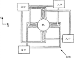
Another solution that liquid-supplying system is proposed is only at the regional area of substrate, and between the last element of projection system and the substrate (this substrate has the surface area bigger than the last element of projection system usually) liquid is provided.A method that addresses this problem that has proposed discloses in WO99/49504, introduces as a reference here.Like Fig. 2 and 3 said, liquid is provided in the substrate by at least one inlet IN, and preferred last relatively element is along the moving direction of substrate, and through projection system down after, export OUT by at least one and remove.That is, when substrate-when directions X scans under element, element+the X side provides liquid, and remove in-X side.Fig. 2 shows schematic setting, and wherein liquid provides through inlet IN, and draws at the opposite side of element through outlet OUT, and this outlet is connected to low pressure source.In the description of Fig. 2, liquid provides along the moving direction of the substrate of last relatively element, though this optional situation.Be positioned at last component ambient various directions and quantity to go into and export be possible, an example wherein in the end provides quadruplet to have the inlet of outlet in each side in the conventional pattern of component ambient shown in Fig. 3.
Another solution be through seal with the regional area of liquid containing in substrate, the sealing part extends along at least a portion edge in the last element of projection system and the space between the base station.Though can exist some to relatively move in Z direction (at optical axis direction), the basic projection system in the XY plane relatively of seal is fixed.Between the surface of seal and substrate, form sealing.As the optimal way sealing is the noncontact sealing, for example hermetic seal.
The character that needs careful control immersion liquid makes its optical property keep constant, and the element that provides and projection system can not polluted by sediment.
Summary of the invention
One object of the present invention is to provide a kind of liquid-supplying system that can control the immersion liquid quality.
Realize this and other purpose according to the present invention in the lithographic projection apparatus that initial paragraph middle finger goes out, this device is characterised in that: said liquid-supplying system comprises the liquid cleaner that is used to purify said immersion liquid.
Like this, lithographic projection apparatus can be connected to ordinary tap water and supply with, and does not need the water source that purifies in advance.Because the cost height of purifying waste water, thereby and need the control surplus it can not discharge, so such scheme is favourable.The present invention can use the immersion liquid except that the projecting beam that is not suitable for the 157nm wavelength.
As optimal way, liquid cleaner comprises (water) distillation unit, and conduct is additional or alternatively, liquid cleaner comprises (water) demineralizer.Like this, the water that is provided by ordinary tap water can supply to lithographic projection apparatus, and there in order to use as immersion liquid, this water becomes purification by the selection of clean unit.Certainly this water can need other adjuvant, for example wetting agent.If immersion liquid is not a water, can need except that distillation unit and demineralizer or the clarifier of other type of replacement distillation unit and demineralizer.
In one embodiment, (water) demineralizer is a reverse osmosis units.
In another embodiment, liquid cleaner comprises filtrator, and this filtrator can dynamically separate with one or more how other parts in the liquid-supplying system.Dynamically separating of this filtrator helps to prevent the particulate crowd dispersion that forms at filtrator and distribute downstream.Thereby can reduce the particle contamination of wafer, output can improve conversely.
As optimal way, liquid-supplying system is included in and need not purifies for the second time under the condition of said immersion liquid, is used for reusing in said space the repetitive cycling device of immersion liquid.The advantage of this system is: owing to can under the condition that need not purify again, reuse immersion liquid, thus can improve the economy of lithographic projection apparatus.
According to another embodiment of the present invention in the lithographic projection apparatus that initial paragraph middle finger goes out, realize this purpose through the described said liquid-supplying system that is used at the ultraviolet light source that gets into the front irradiation immersion liquid of said space that comprises.
Ultraviolet light source except that the projecting beam of lithographic projection apparatus can kill the life entity that in immersion liquid (water), exists effectively, thereby stops further growth.This life entity comprises the algae that pollutes lithographic projection apparatus with other mode.
In the another embodiment of the present invention that also can address the above problem, the lithographic projection apparatus that initial paragraph is pointed out is characterised in that: immersion liquid is opaque to visible light from the conduit that immersion fluid source supplies to said space.For example the life entity of algae needs visible light, thereby they can carry out photosynthesis and growth.Through stoping visible light to arrive immersion liquid, any life entity of light that needs all will be die in the immersion liquid.Like this,, also can keep the quality of immersion liquid, and reduce and pollute even without improvement.
A replacement method that realizes above-mentioned purpose provides the lithographic equipment that the initial paragraph that has liquid-supplying system is pointed out, this system also comprises the device that is used for adding in said immersion liquid life entity growth inhibited chemicals.
In this solution, can kill the for example life entity of algae through chemical attack.
The present invention also be provided at lithographic projection apparatus projection system last element and by the immersion liquid in the space between the substrate that forms images, wherein said immersion liquid comprises water and at least a life entity growth inhibited chemicals.This immersion liquid helps to reduce pollutes, and controls composition easily than the immersion liquid that does not comprise life entity growth inhibited chemicals.
In another embodiment that also addresses the above problem, the lithographic projection apparatus of pointing out at initial paragraph is characterised in that: immersion liquid is the water or the WS, and it has one or more, is preferably whole property (a) and arrives (f):
(a) conductivity of 0.055 little Siemens (microSiemens)/little Siemens/cm of cm to 0.5;
(b) 5 to 8, be preferably 6 to 8 pH value;
(c) 5ppb or still less is preferably 1ppb or organic compound content still less;
(d) in the size of 50nm or in more than every milliliter of immersion liquid, fraction of particle is no more than 2 particulates, preferably is no more than 0.5 particulate;
(e) 15ppb or still less is preferably 5ppb or dissolved oxygen concentration still less; And
(f) 500ppt or still less is preferably 100ppt or dioxide-containing silica still less.
In this embodiment, immersion liquid has high-purity, causes reducing the pollution of various elements in the system of contact liq, and helps avoid optical change or flaw.The immersion liquid of using in the embodiment of the invention can use liquid cleaner to purify, and this clarifier is incorporated into above-mentioned lithographic equipment, or uses remote cleaning system (for example providing filtrator or the clarifier of liquid to lithographic equipment and other user to use point).Particularly, the influence of following one or more difficult problems can avoided or reduce to the device of this embodiment:
-cause water in optical element and/or suprabasil pollution by or discharge immersion liquid dry from element/substrate surface;
-organic species is to the pollution of projection system outer member;
-by in focussing plane or near the particulate or the bubble of focussing plane, causing the printing flaw;
-optics flaw, for example parasitic light;
-through with immersion liquid in material effects damage resist (for example base), and cause the resist surface contamination through the impurity deposition.
A kind of last element of the projection system at the immersion lithographic grenade instrumentation also is provided in the present invention and by the immersion liquid of using between the substrate that forms images, wherein said immersion liquid has one or more, is preferably whole property (a) to (f):
(a) conductivity of 0.055 little Siemens/little Siemens/cm of cm to 0.5;
(b) 5 to 8, be preferably 6 to 8 pH value;
(c) 5ppb or still less is preferably 1ppb or organic compound content still less;
(d) size or the bigger fraction of particle of 50nm is no more than 2 particulates in every milliliter of immersion liquid, preferably is no more than 0.5 particulate;
(e) 15ppb or still less is preferably 5ppb or dissolved oxygen concentration still less; And
(f) 500ppt or still less is preferably 100ppt or dioxide-containing silica still less.
This immersion liquid helps avoid the pollution of water, and helps avoid or reduce difficulty above-mentioned.
According to another aspect of the present invention, a kind of device making method that comprises following step is provided:
-the substrate that provides at least part to cover by radiation-sensitive materials;
-use radiating system that the radiation projecting beam is provided;
-use patterning apparatus to give pattern at the projecting beam xsect;
-patterned radiation laser beam is incident upon the target part of radiation sensitive material layer;
-immersion liquid is provided; The last element of the projection system that the partially filled at least said projection step of this immersion liquid is used and the space between the said substrate; It is characterized in that: provide untreated water to said lithographic projection apparatus; And use liquid cleaner to purify said untreated water, be used for purifying this water immediately before the immersion liquid step is provided said; Or
It is characterized in that: through the opaque conduit of visible light is provided to said space with said immersion liquid from immersion fluid source; Or
It is characterized in that: in said immersion liquid, add at least a life entity growth inhibited chemicals before the immersion liquid step is provided said; Or
It is characterized in that: said immersion liquid is the water or the WS, and it has one or more, is preferably whole property (a) and arrives (f):
(a) conductivity of 0.055 little Siemens/little Siemens/cm of cm to 0.5;
(b) 5 to 8, be preferably 6 to 8 pH value;
(c) 5ppb or still less is preferably 1ppb or organic compound content still less;
(d) size or the bigger fraction of particle of 50nm is no more than 2 particulates in every milliliter of immersion liquid, preferably is no more than 0.5 particulate;
(e) 15ppb or still less is preferably 5ppb or dissolved oxygen concentration still less; And
(f) 500ppt or still less is preferably 100ppt or dioxide-containing silica still less.
Though in this article, detailed reference can clearly be understood these devices and possibly have other application by realizing according to the device of the present invention of making IC.For example, its guiding that can be used for making integrated optics system, be used for magnetic domain memory and check pattern, LCD panel, thin-film head or the like.It should be appreciated by those skilled in the art that; In this interchangeable purposes scope; Any term " reticle " in instructions, " wafer " the perhaps use of " tube core " should think that difference can be by more common term " mask ", and " substrate " and " target part " replaces.
In presents, the term of use " radiation " and " light beam " comprise all types of electromagnetic radiation, comprise UV radiation (for example have 365,248,193,157 or the wavelength of 126nm).
Description of drawings
Existing will be only by way of example mode, with reference to additional schematic figures embodiments of the invention are described.
Fig. 1 shows the lithographic projection apparatus according to the embodiment of the invention;
Fig. 2 shows the liquid containment system according to the embodiment of the invention;
Fig. 3 has illustrated the system of Fig. 3 in the plane;
Fig. 4 shows another liquid containment system according to the embodiment of the invention;
Fig. 5 show according to of the present invention from the water source to the liquid-supplying system of handling.
In the accompanying drawings, corresponding Reference numeral is represented corresponding parts.
Embodiment
Embodiment 1
Fig. 1 has schematically shown a lithographic projection apparatus 1 of the present invention's one specific embodiments.This device comprises:
-radiating system Ex, IL are used to provide radiation projecting beam PB (for example DUV radiation), and in this concrete condition, radiating system also comprises radiation source LA;
-the first object table (mask platform) MT is provided with the mask holder that is used to keep mask MA (for example reticle), and be used for this mask is connected with respect to pinpoint first locating device of object PL;
-the second object table (base station) WT is provided with the substrate holder that is used to keep substrate W (for example applying the silicon wafer of resist), and be used for substrate is connected with respect to pinpoint second locating device of object PL;
-projection system (" camera lens ") PL (for example reflecting system) is used for the radiant section of mask MA is imaged on the target portion C (for example comprising one or more tube cores (die)) of substrate W.
As point out here, this device belongs to transmission-type (promptly having transmission mask)., in general, it can also be a reflection-type (having reflection mask) for example.In addition, this device can utilize the patterning apparatus of other kind, like the above-mentioned array of programmable mirrors type that relates to.
Radiation source LA (for example excimer laser) produces radiation laser beam.This light beam is directly or after passing across like regulating devices such as beam expander Ex, and it is last to be fed to illuminator (luminaire) IL.Luminaire IL can comprise regulating device AM, and the outer and/or interior radius vector that is used to set beam intensity (is called σ-outer and σ-Nei) respectively usually.In addition, it generally comprises various other parts, like integrator IN and condenser CO.In this manner, the light beam PB that shines on the mask MA has required uniformity coefficient and intensity distributions at its xsect.
Should note; Radiation source LA among Fig. 1 can place the housing (for example often being this situation) of lithographic projection apparatus when radiation source LA is mercury lamp; But also can be away from lithographic projection apparatus, the radiation laser beam of its generation is guided in this device by the help of suitable directional mirror (for example through); When light source LA is excimer laser normally the back the sort of situation.The present invention and claim comprise this two kinds of schemes.
Light beam PB intersects with the mask MA that remains on the mask table MT then.After being horizontally through mask MA, light beam PB is through camera lens PL, and this camera lens focuses on light beam PB on the target portion C of substrate W.Assisting down of the second locating device PW (with interferometric measuring means IF), base station WT can accurately move, for example the different target portion C in location in the light path of light beam PB.Similarly, for example after machinery takes out mask MA from the mask storehouse or in scan period, can use the first locating device PM that the light path of the relative light beam PB of mask MA is accurately located.Usually, with long stroke module (coarse localization) that does not clearly show among Fig. 1 and short stroke module (accurately location), can realize moving of object table MT, WT., in wafer stepper (relative with stepping-scanister), mask table MT can be connected with the short stroke actuating device, and is perhaps fixing.Mask MA can use mask alignment mark M1, M2 and substrate alignment mark P1, P2 to aim at substrate W.
Shown device can use according to two kinds of different modes:
1. in step mode, it is motionless that mask table MT keeps basically, and whole mask images is once throwed (i.e. single " sudden strain of a muscle ") on the target portion C.Base station WT moves along x and/or y direction then, so that different target portion C can be shone by light beam PB;
2. in scan pattern, be identical situation basically, but given target portion C is not exposed in single " sudden strain of a muscle ".The substitute is, mask table MT moves with speed v along given direction (so-called " direction of scanning ", for example y direction), so that projecting beam PB scans on mask images; Simultaneously, base station WT moves with speed V=Mv along identical or opposite direction simultaneously, and wherein M is the magnification (M=1/4 or 1/5 usually) of camera lens PL.In this mode, sizable target portion C of can making public, and do not sacrifice resolution.
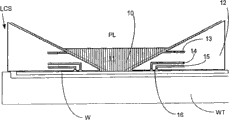
Fig. 4 shows the liquid storage pond 10 between projection system PL and substrate W, and this storage pond is positioned on the base station WT.Liquid storage pond 10 is by high index, and for example the liquid 11 of the particle suspending in water or the water is filled through inlet/outlet pipe 13.The radiation that this liquid plays projecting beam in this liquid than the effect that shorter wavelength is arranged in air or vacuum, to allow to handle littler characteristic.As everyone knows, the resolution limiting of projection system is confirmed by the wavelength of projecting beam and the numerical aperture of system with other parameter.The existence of liquid also can be regarded as increases effective numerical aperture.In addition, under the fixed numeric values aperture, this liquid is used to increase the degree of depth of field.
As optimal way, storage pond 10 forms contactless sealing in projection around the camera lens, thereby this liquid is restricted to the space of filling in the face of between the last optical element of the main surface of the substrate of projection system PL and projection system PL.The storage pond is formed down and around the seal element 12 of this camera lens by the last element that is positioned at projection camera lens PL.Thereby liquid containment system LCS only provides liquid on the regional area of substrate.Seal element 12 forms the part of liquid containment system LCS, is used for the last element of liquid filling projection system and the space between the sensor 10 (or substrate W).This liquid injects under the projection camera lens and the space in the seal element 12.Seal element 12 extends a little above the base member of projection camera lens, and liquid is increased to last element top, thereby liquid buffer is provided.Seal element 12 has inward flange, and this inward flange closely meets the shape of projection system or its last element in the upper end, and can, for example be circular.This inward flange forms the shape in the zone of coincidence imaging closely in the bottom, the aperture of rectangle for example, though this and unnecessary.Projecting beam passes this aperture.
Liquid 11 is limited in the storage pond 10 by air locking 16.As shown in Figure 2, air locking is the noncontact sealing, i.e. hermetic seal.This hermetic seal is by gas, and promptly air or composite air form, and extracts out under low pressure through 15 gaps that supply between seal element 12 and the substrate W that enter the mouth, and by first outlet 14.Settle the overvoltage on the gas access 15, the vacuum levels in first outlet 14 and the geometric configuration in gap, thus exist the two-forty air-flow inwardly to flow towards the optical axis of the device that limits liquid 11.As have any sealing, some liquid possibly overflow, for example in first outlet 14.
Fig. 2 and 3 also shows the liquid that is limited one or more inlet IN, the last element of outlet OUT, substrate W and projection camera lens PL and stores the pond.Similar with the liquid containment system of Fig. 4, Fig. 2 and 3 liquid containment system comprise one or more inlet IN and outlet OUT, the space feed fluid between the regional area on the main surface of the last element of projection system and substrate.
Fig. 2 and 3 and the liquid containment system LCS of Fig. 4 also comprises other scheme, and for example substrate W can both be used with the liquid-supplying system of the present invention shown in Fig. 5 with whole base station WT submergence liquid pools wherein.
Fig. 5 has been shown in further detail liquid-supplying system 100.For example, liquid containment system LCS can be aforesaid any containment.Liquid-supplying system 100 constitutes the part of lithographic projection apparatus.Design this fluid Supplying apparatus, thus for example from the beginning the standard water source 80 at water source can be used as the immersion liquid body source.Yet, also can use other fluid supply, more possibly use the repetitive cycling that is described below in this case, and purification becomes more important.
Before it was suitable as immersion liquid, tap water needed the processing of liquid cleaner.Owing in use can pollute, if therefore other immersion liquid of round-robin words also needs this processing especially.In a preferred embodiment, clarifier can be distillation unit 120 and/or demineralizer 130 and/or unit 140 and/or the filtrator 150 that reduces the hydrocarbons content of liquid.Demineralizer 130 can be any like lower unit, for example: the combination of reverse osmosis units, ion-exchange unit or energising deionization unit or two or more these unit.As typical way, demineralizer reduces the content of water or WS mesoionic compound, thereby electrical conductivity of water is between 0.055 little Siemens/cm and 0.5 little Siemens/cm.Demineralizer also can reduce to 500ppt or still less with dioxide-containing silica, preferably reduces to 100ppt or still less.
The unit 140 that reduces the hydrocarbons content of liquid can be to absorb hydrocarbon (for example charcoal or polymeric material) or by the type of the combination of UV light source and ion-exchanger.As typical way, this unit 140 reduces to 5ppb or still less with the content of the organic compound in the water or the WS, and 3ppb or still less for example preferably reduces to 1ppb or still less, more preferably arrives 0.5ppb or still less.In any case demineralizer 130 can will be removed some hydrocarbons.
As typical way; Filtrator 150 reduces to 2 particulate/milliliters or still less with the fraction of particle of immersion liquid; Be preferably 1 particulate/milliliter or still less, 0.5 particulate/milliliter or still less more preferably, wherein particulate is defined as the particulate with 50nm at least or bigger size.In a preferred embodiment, in filtrator 150 and the liquid-supplying system or more multi-part dynamic isolation.As typical way, filtrator with can cause dynamic isolation in the liquid-supplying system of mechanical shock.For example, filtrator 150 with the flexible pipe in any filtrator downstream and parts can with any parts in the system that causes mechanical shock and/or vibration, for example motor, transfer valve, moving-member and turbulent air dynamic isolation.
Before getting into liquid containment system LCS, liquid preferably reduces parts 160 through gas content.The minimizing of gas content has reduced the possibility that bubble forms, and therefore gas content reduces the effect that parts play bubble minimizing parts.As typical way, gas content reduces parts 160 dissolved oxygen content of immersion liquid is reduced to 15ppb or still less, is preferably 10ppb or still less, or 5ppb or still less.Gas content reduces parts 160 can use the ultrasound wave work of describing in the European Patent Application No. 03253694.8; The document is introduced here as a reference; Or according to identical principle use megahertz level ultrasound wave (approximately 1MHz); This megahertz level ultrasound wave has been avoided more hyperacoustic unfavorable (ultrasound wave can cause that cavitation and bubble and wall collision cause small particle to come off and contaminated liquid from wall).Also can use other gas content to reduce parts, the film that for example those parts of in above-mentioned european patent application, describing, and use possibly combine with vacuum, or through low solubility gas, for example helium purification liquid.Used film from liquid, to remove gas in for example microelectronics, pharmacy and energy applications field.Pumping liquid is through a branch of half porous membrane tube.Set the size in the hole of this film, still can remove gas thereby liquid can not pass them.Thereby liquid is outgased.Can quicken this process through outside pipe, applying low pressure.From USA, North Carolina, the Liqui-Cel that the Membrana-Charlotte of branch of the Celgard Inc. of Charlotte buys
(IM)Membrane Contractors is applicable to this purpose.
Using low solubility gas to purify is known technology, this technical application in high-performance liquid chromatography (HPLC) to prevent that bubble is blocked in the reciprocal pump head.When liquid was passed through in the low solubility gas purification, it evicted other gas from, for example carbon dioxide and oxygen.
After in liquid containment system LCS, using, immersion liquid can be discharged through vent pipe 200.As substitute mode, the immersion liquid of in liquid containment system LCS, having used (or its part) is being passed through or through under all or part of component condition of liquid cleaner, can circulated once more through liquid containment system (through pipeline 115).Liquid cleaner can be made up of other parts, and distillation unit 120, demineralizer 130, unit 140 and filtrator 150 can be with any positioned in sequence.
Also can expect even not passing through the circulation of the immersion liquid of liquid containment system LCS.For example, through one or more behind the multi-part, liquid can be extracted out from liquid cleaner, and through pipeline 115 circulations to get into liquid cleaner again in the position at the upper reaches more.Like this, before getting into liquid containment system, immersion liquid is more than at least one parts of single pass liquid cleaner.This embodiment has the advantage that realizes improving immersion liquid purity.
Through before or after the liquid containment system, the circulation immersion liquid also can make immersion liquid total maintenance flow, even when not through outlet 200 mobile.This helps avoid the existence of stagnant water in the system, and this is an advantage, because know that stagnant water is easy to pollute, for example owing to ooze out from structured material.
In Fig. 5, do not illustrate and be used for the repetitive cycling immersion liquid, to be used for pump at liquid containment system LSC circulating fluid.
The liquid-supplying system 100 of Fig. 5 also has the several measures that reduce or eliminate that are used for the growth of immersion liquid life entity.Can find even the low-down level of this life entity can both cause liquid-supplying system 100 in water source 80 from the beginning pollution.This life entity can comprise algae, bacterium and fungi.
Exist three main method to reduce the growth of this life entity shown in Fig. 5.Should be appreciated that and to use these methods individually or with any array mode.To algae and the effective first method of other green plants is to guarantee that liquid does not receive radiation of visible light, and the conduit 110,115 of for example guaranteeing the transporting water in the liquid-supplying system 100 is by to the opaque made of visible light.As substitute mode, whole liquid feed system 100 or even whole device can be housed in opaque container of visible light or the outer cover (for example room) 180.As substitute mode, conduit 110 can cover can not transmit the material of visible light.Like this, the biosome in the water can not carry out photosynthesis, therefore can not grow or increase.The non-permeable material of suitable visible light is stainless steel, polymkeric substance etc.
Fig. 5 also shows the use of the ultraviolet light source 145 that is used to shine immersion liquid.Through before the liquid containment system LCS, UV light source 145 is used to shine this liquid at liquid, thereby this light source is the separation irradiation system to the projecting beam PB of the substrate W that is used to form images.UV light source 145 can be arranged in any position of liquid containment system LCS liquid upstream feed system 100.The UV light source will kill life entity, and this life entity is removed from liquid by the for example particulate filter of filtrator 150 subsequently.Though also can use for example other size of 0.1 to 0.2 μ m, the hole that filtrator is suitable is of a size of 0.03 to 2.0 μ m.
The other method that reduces life entity influence on the lithographic projection apparatus is that (this immersion liquid is a water under the situation shown in Fig. 5) adds life entity growth inhibited chemical agent in immersion liquid.This realizes that through using life entity growth inhibited chemical agent adding set 147 this device can be positioned at the upper reaches or the downstream of any other parts 120,130,140,145,150,160 of liquid-supplying system.Typical chemical agent is compound (being generally the chlorine or bromine base), alcohol, acetaldehyde, ozone and the heavy metal that comprises halogen.The dosage of any this chemical agent is preferably very low, to guarantee to meet immersion liquid purity needs.
Certainly, adding set 147 also can add other chemicals to immersion liquid, for example surfactant and wetting agent.
Be filtered with the last degassing (that is, removing bubble) preceding, although the embodiment among Fig. 5 shows the immersion liquid that at first is distilled, demineralization then, dehydrochlorination then, and then by the UV irradiation, this can take place with any order.In addition, chemicals can add in the entry in any upstream phase of liquid closed system LCS, and repetitive cycling water also can be added in any upstream phase of liquid closed system LCS.The stage that repetitive cycling water adds is based on its purity.In the example shown in Fig. 5, solid line representes that repetitive cycling water adds the downstream that adding set 147, distillation unit 120, demineralization unit 130, unit 140, UV light source 145, filtrator 150 and gas content reduce device 160.Be shown in dotted line the replacement position that circulating fluid can add.Circulating fluid preferably is added to the upper reaches of filtrator 150 at least.
In one embodiment of the invention, liquid cleaner purifies the immersion liquid for the water or the WS, thereby that immersion liquid has is one or more, be preferably whole above-mentioned character (a) to (f).In the preferred embodiment of the invention, that immersion liquid has is one or more, be preferably whole property (a) to (f):
(a) conductivity of 0.055 little Siemens/little Siemens/cm of cm to 0.5;
(b) 6 to 8 pH value;
(c) 1ppb or organic compound content still less;
(d) size or the bigger fraction of particle of 50nm is no more than 0.5 particulate in every milliliter of immersion liquid;
(e) 5ppb or dissolved oxygen concentration still less; And
(f) 100ppt or dioxide-containing silica still less.
Use demineralizer, for example ion-exchange unit or energising deionization unit are typically controlled the conductivity of immersion liquid, thereby conductivity is between the little Siemens/cm of 0.055 little Siemens/cm to 0.5.In a preferred embodiment, conductivity is 0.3 little Siemens/cm or littler, for example 0.1 little Siemens/cm or littler.Demineralizer also can be used in the dioxide-containing silica in the control immersion liquid.Preferred dioxide-containing silica is 500ppt or still less, 200ppt or still less for example, and 100ppt or still less, 90ppt or still less, or even be 80ppt or still less.
The pH value of immersion liquid can be by any suitable device control.Typically, if use with the liquid cleaner purified tap water that meets the foregoing description, the pH value will be in preferred range 5 to 8, and more preferably 6 to 8.If in immersion liquid, comprise adjuvant, should control the amount of this adjuvant, thereby the pH value of immersion liquid remains between 5 and 8.As substitute mode, can be by realizing required pH value through adding suitable reducing.Preferred mode is for controlling the pH value through the existence that limits the parts that can change water or pH value of aqueous solution.First-selected interpolation is buffering agent for example, because the existence of buffering agent can otherwise influence the purity of immersion liquid.
The concentration of organic compound is typically by unit 140 controls that are used to reduce hydrocarbons content in the immersion liquid.Same, the quantity that is present in the particulate in the immersion liquid can be used filtrator control.The fraction of particle of immersion liquid is the fraction of particle that has greater than minimum feature size in the photoetching process.Thereby fraction of particle is to have 50nm or larger sized fraction of particle at least.
The oxygen content typical case of immersion liquid uses above-mentioned gas content to reduce device control.Preferably, oxygen content reduces to 15ppb or still less, 10ppb or still less for example, 7ppb or still less, 4ppb or still less, or even 3ppb or still less.
Liquid-supplying system 100 can comprise one or more character (a) of being used for measuring immersion liquid measurement mechanism (Fig. 5 is not shown) to (f) selectively.For example, this measurement mechanism can be positioned at least one of fluid Supplying apparatus, or the preferred whole parts 120,130,140,145,150 and 160 the upper reaches.Also can use the off line measurement mechanism, wherein the sample of water suitable sampling spot from liquid-supplying system extracts, and supplies to the measurement mechanism of off line.In one embodiment, measurement mechanism will comprise one or more devices of selecting from the device that is used for conductivity, pH sensor, TOC (total organic carbon) analyzer, batch particle-counting system, lambda sensor and overall silicon measuring element.Also can use the bubble measurement mechanism.Those of ordinary skills know and are used to measure the appropriate technology of various character (a) to (f).
When specific embodiments of the present invention is described, be to be understood that the present invention can be by except that the mode of describing, realizing in the above.Instructions is not meaned restriction the present invention.
Claims (18)
1. lithographic projection apparatus comprises:
Be used to provide the radiating system of radiation projecting beam;
Be used to support the supporting construction of patterning apparatus, said patterning apparatus is used for according to required pattern projecting beam being carried out composition;
Be used to keep the base station of substrate;
Be used for patterned radiation laser beam is projected the projection system on the target part of substrate;
Be used for the last element of the partially filled at least said projection system of immersion liquid and the liquid-supplying system in the space between the said substrate, said liquid-supplying system comprises the liquid cleaner that is used to purify said immersion liquid,
Wherein said liquid cleaner comprises the degas module that the upper reaches that are positioned at said space do not contact with said space; And said liquid-supplying system forms contactless sealing around the projection camera lens of said projection system, thus said immersion liquid be restricted to fill and the last element of the main surface of the substrate that said projection system is faced and said projection system between the space.
2. according to the lithographic projection apparatus of claim 1, wherein said degas module comprises film.
3. according to the lithographic projection apparatus of claim 2, wherein said film is half porous membrane tube.
4. according to the lithographic projection apparatus of aforementioned each claim, wherein said degas module comprises use ultrasound wave or megahertz level ultrasound wave.
5. according to each the described lithographic projection apparatus among the claim 1-3, wherein said degas module is configured to utilize the said immersion liquid of low solubility gas purification.
6. according to each the described lithographic projection apparatus among the claim 1-3, wherein said degas module is reduced to 15ppb or still less with the dissolved oxygen concentration of said immersion liquid.
7. according to each the described lithographic projection apparatus among the claim 1-3, wherein said liquid-supplying system comprises measurement mechanism.
8. according to the lithographic projection apparatus of claim 7, wherein said measurement mechanism comprises lambda sensor.
9. according to the lithographic projection apparatus of claim 7, wherein said measurement mechanism is positioned at the downstream of said degas module.
10. according to each the described lithographic projection apparatus among the claim 1-3, wherein said liquid cleaner comprises filtrator.
11. according to each the described lithographic projection apparatus among the claim 1-3, wherein said immersion liquid flow to drainpipe after flowing through said space.
12. according to each the described lithographic projection apparatus among the claim 1-3, wherein said liquid-supplying system is included in the ultraviolet light source that immersion liquid gets into the said immersion liquid of said space front irradiation.
13. according to each the described lithographic projection apparatus among the claim 1-3, wherein said liquid-supplying system comprises container or to the outer cover of the said liquid-supplying system of the nontransparent encirclement of visible light.
14. according to each the described lithographic projection apparatus among the claim 1-3, wherein said liquid-supplying system comprises immersion liquid is provided to the conduit in said space from immersion fluid source that this conduit is nontransparent to visible light.
15. each the described lithographic projection apparatus according among the claim 1-3 further comprises batch particle-counting system.
16. a lithographic projection apparatus comprises:
Be used to provide the radiating system of radiation projecting beam;
Be used to support the supporting construction of patterning apparatus, said patterning apparatus is used for according to required pattern projecting beam being carried out composition;
Be used to keep the base station of substrate;
Be used for patterned radiation laser beam is projected the projection system on the target part of substrate;
Be used for the last element of the partially filled at least said projection system of immersion liquid and the liquid-supplying system in the space between the said substrate,
It is characterized in that: provide to prevent that said immersion liquid is by the device of radiation of visible light; And said liquid-supplying system forms contactless sealing around the projection camera lens of said projection system, thus said immersion liquid be restricted to fill and the last element of the main surface of the substrate that said projection system is faced and said projection system between the space.
17. a lithographic projection apparatus comprises:
Be used to provide the radiating system of radiation projecting beam;
Be used to support the supporting construction of patterning apparatus, said patterning apparatus is used for according to required pattern projecting beam being carried out composition;
Be used to keep the base station of substrate;
Be used for patterned radiation laser beam is projected the projection system on the target part of substrate;
Be used for the last element of the partially filled at least said projection system of immersion liquid and the liquid-supplying system in the space between the said substrate, and
Be used to measure the measurement mechanism of the character of said immersion liquid; And said liquid-supplying system forms contactless sealing around the projection camera lens of said projection system, thus said immersion liquid be restricted to fill and the last element of the main surface of the substrate that said projection system is faced and said projection system between the space.
18. a lithographic projection apparatus comprises:
Be used to provide the radiating system of radiation projecting beam;
Be used to support the supporting construction of patterning apparatus, said patterning apparatus is used for according to required pattern projecting beam being carried out composition;
Be used to keep the base station of substrate;
Be used for patterned radiation laser beam is projected the projection system on the target part of substrate; And
Be used for the last element of the partially filled at least said projection system of immersion liquid and the liquid-supplying system in the space between the said substrate, said liquid-supplying system comprises and is used for batch particle-counting system that the particulate of said immersion liquid is counted; And said liquid-supplying system forms contactless sealing around the projection camera lens of said projection system, thus said immersion liquid be restricted to fill and the last element of the main surface of the substrate that said projection system is faced and said projection system between the space.
Applications Claiming Priority (2)
| Application Number | Priority Date | Filing Date | Title |
|---|---|---|---|
| EP03255376 | 2003-08-29 | ||
| EP03255376.0 | 2003-08-29 |
Related Parent Applications (1)
| Application Number | Title | Priority Date | Filing Date |
|---|---|---|---|
| CN2004100682666A Division CN1591192B (en) | 2003-08-29 | 2004-08-27 | Lithographic apparatus and device manufacturing method |
Publications (2)
| Publication Number | Publication Date |
|---|---|
| CN101872130A CN101872130A (en) | 2010-10-27 |
| CN101872130B true CN101872130B (en) | 2012-10-03 |
Family
ID=34400571
Family Applications (2)
| Application Number | Title | Priority Date | Filing Date |
|---|---|---|---|
| CN2010101140186A Expired - Fee Related CN101872130B (en) | 2003-08-29 | 2004-08-27 | Lithographic projection apparatus |
| CN2004100682666A Expired - Fee Related CN1591192B (en) | 2003-08-29 | 2004-08-27 | Lithographic apparatus and device manufacturing method |
Family Applications After (1)
| Application Number | Title | Priority Date | Filing Date |
|---|---|---|---|
| CN2004100682666A Expired - Fee Related CN1591192B (en) | 2003-08-29 | 2004-08-27 | Lithographic apparatus and device manufacturing method |
Country Status (8)
| Country | Link |
|---|---|
| US (6) | US7733459B2 (en) |
| EP (3) | EP1510872B1 (en) |
| JP (5) | JP2005079584A (en) |
| KR (1) | KR100659257B1 (en) |
| CN (2) | CN101872130B (en) |
| DE (1) | DE602004029970D1 (en) |
| SG (1) | SG109609A1 (en) |
| TW (1) | TWI245163B (en) |
Families Citing this family (122)
| Publication number | Priority date | Publication date | Assignee | Title |
|---|---|---|---|---|
| DE10261775A1 (en) | 2002-12-20 | 2004-07-01 | Carl Zeiss Smt Ag | Device for the optical measurement of an imaging system |
| EP3226073A3 (en) | 2003-04-09 | 2017-10-11 | Nikon Corporation | Exposure method and apparatus, and method for fabricating device |
| SG185136A1 (en) * | 2003-04-11 | 2012-11-29 | Nikon Corp | Cleanup method for optics in immersion lithography |
| KR101225884B1 (en) | 2003-04-11 | 2013-01-28 | 가부시키가이샤 니콘 | Apparatus and method for maintaining immersion fluid in the gap under the projection lens during wafer exchange in an immersion lithography machine |
| TW200509205A (en) * | 2003-05-23 | 2005-03-01 | Nippon Kogaku Kk | Exposure method and device-manufacturing method |
| TWI347741B (en) * | 2003-05-30 | 2011-08-21 | Asml Netherlands Bv | Lithographic apparatus and device manufacturing method |
| EP2261741A3 (en) * | 2003-06-11 | 2011-05-25 | ASML Netherlands B.V. | Lithographic apparatus and device manufacturing method |
| KR101940892B1 (en) | 2003-06-13 | 2019-01-21 | 가부시키가이샤 니콘 | Exposure method, substrate stage, exposure apparatus and method for manufacturing device |
| US6867844B2 (en) | 2003-06-19 | 2005-03-15 | Asml Holding N.V. | Immersion photolithography system and method using microchannel nozzles |
| KR101289979B1 (en) | 2003-06-19 | 2013-07-26 | 가부시키가이샤 니콘 | Exposure device and device producing method |
| EP1491956B1 (en) | 2003-06-27 | 2006-09-06 | ASML Netherlands B.V. | Lithographic apparatus and device manufacturing method |
| US6809794B1 (en) * | 2003-06-27 | 2004-10-26 | Asml Holding N.V. | Immersion photolithography system and method using inverted wafer-projection optics interface |
| US7579135B2 (en) * | 2003-08-11 | 2009-08-25 | Taiwan Semiconductor Manufacturing Company, Ltd. | Lithography apparatus for manufacture of integrated circuits |
| US7700267B2 (en) * | 2003-08-11 | 2010-04-20 | Taiwan Semiconductor Manufacturing Company, Ltd. | Immersion fluid for immersion lithography, and method of performing immersion lithography |
| TWI245163B (en) | 2003-08-29 | 2005-12-11 | Asml Netherlands Bv | Lithographic apparatus and device manufacturing method |
| SG145780A1 (en) * | 2003-08-29 | 2008-09-29 | Nikon Corp | Exposure apparatus and device fabricating method |
| TWI263859B (en) | 2003-08-29 | 2006-10-11 | Asml Netherlands Bv | Lithographic apparatus and device manufacturing method |
| WO2005029559A1 (en) * | 2003-09-19 | 2005-03-31 | Nikon Corporation | Exposure apparatus and device producing method |
| TW201809911A (en) * | 2003-09-29 | 2018-03-16 | 尼康股份有限公司 | Exposure apparatus, exposure method, and method for producing device |
| KR101319109B1 (en) * | 2003-10-08 | 2013-10-17 | 가부시키가이샤 자오 니콘 | Substrate carrying apparatus, substrate carrying method, exposure apparatus, exposure method, and method for producing device |
| WO2005036623A1 (en) | 2003-10-08 | 2005-04-21 | Zao Nikon Co., Ltd. | Substrate transporting apparatus and method, exposure apparatus and method, and device producing method |
| JP2005136364A (en) * | 2003-10-08 | 2005-05-26 | Zao Nikon Co Ltd | Substrate carrying device, exposure device and device manufacturing method |
| TWI598934B (en) | 2003-10-09 | 2017-09-11 | Nippon Kogaku Kk | Exposure apparatus, exposure method, and device manufacturing method |
| DE602004030365D1 (en) | 2003-10-22 | 2011-01-13 | Nippon Kogaku Kk | EXPOSURE DEVICE, EXPOSURE METHOD AND METHOD FOR MANUFACTURING COMPONENTS |
| TWI609409B (en) | 2003-10-28 | 2017-12-21 | 尼康股份有限公司 | Optical illumination device, exposure device, exposure method and device manufacturing method |
| JP4295712B2 (en) | 2003-11-14 | 2009-07-15 | エーエスエムエル ネザーランズ ビー.ブイ. | Lithographic apparatus and apparatus manufacturing method |
| TWI512335B (en) | 2003-11-20 | 2015-12-11 | 尼康股份有限公司 | Light beam converter, optical illuminating apparatus, exposure device, and exposure method |
| TWI440981B (en) | 2003-12-03 | 2014-06-11 | 尼康股份有限公司 | Exposure apparatus, exposure method, and device manufacturing method |
| KR101111363B1 (en) * | 2003-12-15 | 2012-04-12 | 가부시키가이샤 니콘 | Projection exposure apparatus, stage apparatus, and exposure method |
| KR101941351B1 (en) | 2003-12-15 | 2019-01-22 | 가부시키가이샤 니콘 | Stage system, exposure apparatus and exposure method |
| US20070081133A1 (en) * | 2004-12-14 | 2007-04-12 | Niikon Corporation | Projection exposure apparatus and stage unit, and exposure method |
| JP4323946B2 (en) * | 2003-12-19 | 2009-09-02 | キヤノン株式会社 | Exposure equipment |
| WO2005071717A1 (en) * | 2004-01-26 | 2005-08-04 | Nikon Corporation | Exposure apparatus and device producing method |
| US7589822B2 (en) * | 2004-02-02 | 2009-09-15 | Nikon Corporation | Stage drive method and stage unit, exposure apparatus, and device manufacturing method |
| EP1713114B1 (en) * | 2004-02-03 | 2018-09-19 | Nikon Corporation | Exposure apparatus and device manufacturing method |
| TWI614795B (en) | 2004-02-06 | 2018-02-11 | Nikon Corporation | Optical illumination apparatus, light-exposure apparatus, light-exposure method and device manufacturing method |
| US8488102B2 (en) * | 2004-03-18 | 2013-07-16 | Taiwan Semiconductor Manufacturing Company, Ltd. | Immersion fluid for immersion lithography, and method of performing immersion lithography |
| JP3981368B2 (en) * | 2004-05-17 | 2007-09-26 | 松下電器産業株式会社 | Pattern formation method |
| WO2005119368A2 (en) | 2004-06-04 | 2005-12-15 | Carl Zeiss Smt Ag | System for measuring the image quality of an optical imaging system |
| CN103605262B (en) * | 2004-06-09 | 2016-06-29 | 株式会社尼康 | Exposure device and maintaining method thereof and manufacturing method |
| US7463330B2 (en) | 2004-07-07 | 2008-12-09 | Asml Netherlands B.V. | Lithographic apparatus and device manufacturing method |
| US20060044533A1 (en) * | 2004-08-27 | 2006-03-02 | Asmlholding N.V. | System and method for reducing disturbances caused by movement in an immersion lithography system |
| KR101559621B1 (en) * | 2004-12-06 | 2015-10-13 | 가부시키가이샤 니콘 | Maintenance method, maintenance apparatus, exposure apparatus and device manufacturing method |
| JP4752473B2 (en) * | 2004-12-09 | 2011-08-17 | 株式会社ニコン | Exposure apparatus, exposure method, and device manufacturing method |
| EP1843387A4 (en) * | 2005-01-25 | 2010-01-13 | Jsr Corp | Immersion exposure system, and recycle method and supply method of liquid for immersion exposure |
| US7428038B2 (en) * | 2005-02-28 | 2008-09-23 | Asml Netherlands B.V. | Lithographic apparatus, device manufacturing method and apparatus for de-gassing a liquid |
| US7282701B2 (en) * | 2005-02-28 | 2007-10-16 | Asml Netherlands B.V. | Sensor for use in a lithographic apparatus |
| US7324185B2 (en) | 2005-03-04 | 2008-01-29 | Asml Netherlands B.V. | Lithographic apparatus and device manufacturing method |
| JP4072543B2 (en) * | 2005-03-18 | 2008-04-09 | キヤノン株式会社 | Immersion exposure apparatus and device manufacturing method |
| USRE43576E1 (en) | 2005-04-08 | 2012-08-14 | Asml Netherlands B.V. | Dual stage lithographic apparatus and device manufacturing method |
| US7291850B2 (en) * | 2005-04-08 | 2007-11-06 | Asml Netherlands B.V. | Lithographic apparatus and device manufacturing method |
| US20060232753A1 (en) * | 2005-04-19 | 2006-10-19 | Asml Holding N.V. | Liquid immersion lithography system with tilted liquid flow |
| US8248577B2 (en) | 2005-05-03 | 2012-08-21 | Asml Netherlands B.V. | Lithographic apparatus and device manufacturing method |
| US7315033B1 (en) * | 2005-05-04 | 2008-01-01 | Advanced Micro Devices, Inc. | Method and apparatus for reducing biological contamination in an immersion lithography system |
| EP3232270A3 (en) | 2005-05-12 | 2017-12-13 | Nikon Corporation | Projection optical system, exposure apparatus, and exposure method |
| JP4596191B2 (en) * | 2005-05-24 | 2010-12-08 | 株式会社ニコン | Exposure method, exposure apparatus, and device manufacturing method |
| US7652746B2 (en) * | 2005-06-21 | 2010-01-26 | Asml Netherlands B.V. | Lithographic apparatus and device manufacturing method |
| US20070004182A1 (en) * | 2005-06-30 | 2007-01-04 | Taiwan Semiconductor Manufacturing Company, Ltd. | Methods and system for inhibiting immersion lithography defect formation |
| JP5040653B2 (en) * | 2005-08-23 | 2012-10-03 | 株式会社ニコン | Exposure apparatus, exposure method, and device manufacturing method |
| US20070058263A1 (en) * | 2005-09-13 | 2007-03-15 | Taiwan Semiconductor Manufacturing Company, Ltd. | Apparatus and methods for immersion lithography |
| US7420188B2 (en) * | 2005-10-14 | 2008-09-02 | Taiwan Semiconductor Manufacturing Company, Ltd. | Exposure method and apparatus for immersion lithography |
| US7986395B2 (en) * | 2005-10-24 | 2011-07-26 | Taiwan Semiconductor Manufacturing Company, Ltd. | Immersion lithography apparatus and methods |
| KR20080070681A (en) * | 2005-11-23 | 2008-07-30 | 이 아이 듀폰 디 네모아 앤드 캄파니 | Apparatus for recycling alkane immersion liquids and methods of employment |
| US7773195B2 (en) * | 2005-11-29 | 2010-08-10 | Asml Holding N.V. | System and method to increase surface tension and contact angle in immersion lithography |
| US8125610B2 (en) | 2005-12-02 | 2012-02-28 | ASML Metherlands B.V. | Method for preventing or reducing contamination of an immersion type projection apparatus and an immersion type lithographic apparatus |
| US20070124987A1 (en) * | 2005-12-05 | 2007-06-07 | Brown Jeffrey K | Electronic pest control apparatus |
| EP1965414A4 (en) * | 2005-12-06 | 2010-08-25 | Nikon Corp | Exposure method, exposure apparatus, and method for manufacturing device |
| TW200725196A (en) * | 2005-12-19 | 2007-07-01 | Nikon Corp | Liquid producing apparatus, liquid immersion exposure apparatus, and unit manufacturing method |
| US7714980B2 (en) * | 2006-02-15 | 2010-05-11 | Canon Kabushiki Kaisha | Exposure apparatus, exposure method, and exposure system |
| JP2007242774A (en) * | 2006-03-07 | 2007-09-20 | Canon Inc | Exposure equipment and method therefor, and device manufacturing method |
| CN100590173C (en) * | 2006-03-24 | 2010-02-17 | 北京有色金属研究总院 | Fluorescent powder and manufacturing method and electric light source produced thereby |
| JP2007286162A (en) * | 2006-04-13 | 2007-11-01 | Nikon Corp | Immersion microscopic device |
| US8564759B2 (en) * | 2006-06-29 | 2013-10-22 | Taiwan Semiconductor Manufacturing Company, Ltd. | Apparatus and method for immersion lithography |
| JP2009545136A (en) * | 2006-07-21 | 2009-12-17 | インテグリス・インコーポレーテッド | Apparatus and method for conditioning immersion fluid |
| US7826030B2 (en) * | 2006-09-07 | 2010-11-02 | Asml Netherlands B.V. | Lithographic apparatus and device manufacturing method |
| US20080198347A1 (en) * | 2007-02-16 | 2008-08-21 | Canon Kabushiki Kaisha | Immersion exposure apparatus and method of manufacturing device |
| JP2010519722A (en) * | 2007-02-23 | 2010-06-03 | 株式会社ニコン | Exposure method, exposure apparatus, device manufacturing method, and immersion exposure substrate |
| US9025126B2 (en) * | 2007-07-31 | 2015-05-05 | Nikon Corporation | Exposure apparatus adjusting method, exposure apparatus, and device fabricating method |
| SG151198A1 (en) * | 2007-09-27 | 2009-04-30 | Asml Netherlands Bv | Methods relating to immersion lithography and an immersion lithographic apparatus |
| JP5267029B2 (en) | 2007-10-12 | 2013-08-21 | 株式会社ニコン | Illumination optical apparatus, exposure apparatus, and device manufacturing method |
| US8379187B2 (en) | 2007-10-24 | 2013-02-19 | Nikon Corporation | Optical unit, illumination optical apparatus, exposure apparatus, and device manufacturing method |
| US9116346B2 (en) | 2007-11-06 | 2015-08-25 | Nikon Corporation | Illumination apparatus, illumination method, exposure apparatus, and device manufacturing method |
| KR101423611B1 (en) * | 2008-01-16 | 2014-07-30 | 삼성전자주식회사 | Substrate treating apparatus, exposing apparatus, and cleaning method of cleaning tool |
| NL1036432A1 (en) * | 2008-01-23 | 2009-07-27 | Asml Holding Nv | An immersion lithographic apparatus with immersion fluid re-circulating system. |
| JP2009218344A (en) * | 2008-03-10 | 2009-09-24 | Canon Inc | Exposing apparatus and exposing method |
| NL1036766A1 (en) * | 2008-04-25 | 2009-10-27 | Asml Netherlands Bv | Methods related to immersion lithography and an immersion lithographic apparatus. |
| EP2128703A1 (en) | 2008-05-28 | 2009-12-02 | ASML Netherlands BV | Lithographic Apparatus and a Method of Operating the Apparatus |
| NL2004540A (en) * | 2009-05-14 | 2010-11-18 | Asml Netherlands Bv | Lithographic apparatus and a method of operating the apparatus. |
| NL2005207A (en) | 2009-09-28 | 2011-03-29 | Asml Netherlands Bv | Heat pipe, lithographic apparatus and device manufacturing method. |
| CA3085086C (en) | 2011-12-06 | 2023-08-08 | Delta Faucet Company | Ozone distribution in a faucet |
| US9017934B2 (en) | 2013-03-08 | 2015-04-28 | Taiwan Semiconductor Manufacturing Company, Ltd. | Photoresist defect reduction system and method |
| US9110376B2 (en) | 2013-03-12 | 2015-08-18 | Taiwan Semiconductor Manufacturing Company, Ltd. | Photoresist system and method |
| US9175173B2 (en) | 2013-03-12 | 2015-11-03 | Taiwan Semiconductor Manufacturing Company, Ltd. | Unlocking layer and method |
| US9245751B2 (en) | 2013-03-12 | 2016-01-26 | Taiwan Semiconductor Manufacturing Company, Ltd. | Anti-reflective layer and method |
| US8932799B2 (en) | 2013-03-12 | 2015-01-13 | Taiwan Semiconductor Manufacturing Company, Ltd. | Photoresist system and method |
| US9543147B2 (en) | 2013-03-12 | 2017-01-10 | Taiwan Semiconductor Manufacturing Company, Ltd. | Photoresist and method of manufacture |
| US9256128B2 (en) | 2013-03-12 | 2016-02-09 | Taiwan Semiconductor Manufacturing Company, Ltd. | Method for manufacturing semiconductor device |
| US9502231B2 (en) | 2013-03-12 | 2016-11-22 | Taiwan Semiconductor Manufacturing Company, Ltd. | Photoresist layer and method |
| US9354521B2 (en) | 2013-03-12 | 2016-05-31 | Taiwan Semiconductor Manufacturing Company, Ltd. | Photoresist system and method |
| US9117881B2 (en) | 2013-03-15 | 2015-08-25 | Taiwan Semiconductor Manufacturing Company, Ltd. | Conductive line system and process |
| KR102101350B1 (en) * | 2013-03-15 | 2020-04-17 | 삼성전자주식회사 | particle counter and immersion scanner used the same |
| US9341945B2 (en) | 2013-08-22 | 2016-05-17 | Taiwan Semiconductor Manufacturing Company, Ltd. | Photoresist and method of formation and use |
| US10036953B2 (en) | 2013-11-08 | 2018-07-31 | Taiwan Semiconductor Manufacturing Company | Photoresist system and method |
| US10095113B2 (en) | 2013-12-06 | 2018-10-09 | Taiwan Semiconductor Manufacturing Company | Photoresist and method |
| US9761449B2 (en) | 2013-12-30 | 2017-09-12 | Taiwan Semiconductor Manufacturing Company, Ltd. | Gap filling materials and methods |
| US9599896B2 (en) | 2014-03-14 | 2017-03-21 | Taiwan Semiconductor Manufacturing Company, Ltd. | Photoresist system and method |
| DE102014004511A1 (en) * | 2014-03-28 | 2015-10-01 | Carl Zeiss Microscopy Gmbh | Method for terminating microscopic applications with an immersion objective |
| WO2015158444A1 (en) * | 2014-04-14 | 2015-10-22 | Asml Netherlands B.V. | Flows of optimization for lithographic processes |
| US9581908B2 (en) | 2014-05-16 | 2017-02-28 | Taiwan Semiconductor Manufacturing Company, Ltd. | Photoresist and method |
| DE102015218053A1 (en) * | 2015-09-21 | 2017-03-23 | Eta Plus Electronic Gmbh | Device for UV irradiation of a flowing medium |
| US11358172B2 (en) | 2015-09-24 | 2022-06-14 | Suss Microtec Photomask Equipment Gmbh & Co. Kg | Method for treating substrates with an aqueous liquid medium exposed to UV-radiation |
| WO2017112795A1 (en) | 2015-12-21 | 2017-06-29 | Delta Faucet Company | Fluid delivery system including a disinfectant device |
| IL265376B1 (en) | 2016-09-20 | 2024-04-01 | Aqua Membranes Llc | Permeate flow patterns |
| WO2018094287A1 (en) | 2016-11-19 | 2018-05-24 | Aqua Membranes Llc | Interfernce patterns for spiral-wound elements |
| US11090612B2 (en) | 2017-04-12 | 2021-08-17 | Aqua Membranes Inc. | Graded spacers for filtration wound elements |
| CN206881955U (en) * | 2017-04-17 | 2018-01-16 | 福建西河卫浴科技有限公司 | One kind centrifugation aproll structure and gondola water faucet |
| JP2020517423A (en) | 2017-04-20 | 2020-06-18 | アクア メンブレインズ,インコーポレイテッド | Non-nesting, non-deformed pattern for spiral wound elements |
| US11745143B2 (en) | 2017-04-20 | 2023-09-05 | Aqua Membranes, Inc. | Mixing-promoting spacer patterns for spiral-wound elements |
| US11745144B2 (en) | 2017-10-13 | 2023-09-05 | Aqua Membranes Inc. | Bridge support and reduced feed spacers for spiral-wound elements |
| CN111432906A (en) * | 2017-12-04 | 2020-07-17 | 株式会社岛津制作所 | Method and apparatus for removing fine bubbles, and method and apparatus for measuring bubble diameter distribution |
| JP2023521977A (en) | 2020-04-07 | 2023-05-26 | アクア メンブレインズ,インコーポレイテッド | Independent spacer and method |
| CN112650031A (en) * | 2020-12-25 | 2021-04-13 | 浙江启尔机电技术有限公司 | Immersion liquid supply apparatus, lithography system, and immersion liquid quality monitoring method |
Citations (4)
| Publication number | Priority date | Publication date | Assignee | Title |
|---|---|---|---|---|
| US4480910A (en) * | 1981-03-18 | 1984-11-06 | Hitachi, Ltd. | Pattern forming apparatus |
| US5610683A (en) * | 1992-11-27 | 1997-03-11 | Canon Kabushiki Kaisha | Immersion type projection exposure apparatus |
| US5900354A (en) * | 1997-07-03 | 1999-05-04 | Batchelder; John Samuel | Method for optical inspection and lithography |
| US6423223B1 (en) * | 2000-08-31 | 2002-07-23 | Donald A. Northcut | Multi-element, reverse osmosis, liquid filter system with flushing and filtering circuits |
Family Cites Families (225)
| Publication number | Priority date | Publication date | Assignee | Title |
|---|---|---|---|---|
| DE221563C (en) | ||||
| DE206607C (en) | ||||
| DE224448C (en) | ||||
| DE242880C (en) | ||||
| GB1242527A (en) | 1967-10-20 | 1971-08-11 | Kodak Ltd | Optical instruments |
| US3573975A (en) | 1968-07-10 | 1971-04-06 | Ibm | Photochemical fabrication process |
| ATE1462T1 (en) | 1979-07-27 | 1982-08-15 | Werner W. Dr. Tabarelli | OPTICAL LITHOGRAPHY PROCESS AND DEVICE FOR COPYING A PATTERN ONTO A SEMICONDUCTOR DISC. |
| FR2474708B1 (en) | 1980-01-24 | 1987-02-20 | Dme | HIGH-RESOLUTION MICROPHOTOLITHOGRAPHY PROCESS |
| JPS5754317A (en) | 1980-09-19 | 1982-03-31 | Hitachi Ltd | Method and device for forming pattern |
| US4346164A (en) | 1980-10-06 | 1982-08-24 | Werner Tabarelli | Photolithographic method for the manufacture of integrated circuits |
| US4509852A (en) | 1980-10-06 | 1985-04-09 | Werner Tabarelli | Apparatus for the photolithographic manufacture of integrated circuit elements |
| US4390273A (en) | 1981-02-17 | 1983-06-28 | Censor Patent-Und Versuchsanstalt | Projection mask as well as a method and apparatus for the embedding thereof and projection printing system |
| JPS58202448A (en) | 1982-05-21 | 1983-11-25 | Hitachi Ltd | Exposing device |
| JPH0747157B2 (en) | 1985-02-15 | 1995-05-24 | 株式会社日立製作所 | Ultrapure water production system |
| JPS61187984U (en) | 1985-05-15 | 1986-11-22 | ||
| JPS6265326A (en) | 1985-09-18 | 1987-03-24 | Hitachi Ltd | Exposure device |
| JPS6265326U (en) | 1985-10-16 | 1987-04-23 | ||
| JPS62121417A (en) | 1985-11-22 | 1987-06-02 | Hitachi Ltd | Liquid-immersion objective lens device |
| JPS62121417U (en) | 1986-01-24 | 1987-08-01 | ||
| JPS63108724A (en) * | 1986-10-27 | 1988-05-13 | Japan Organo Co Ltd | Manufacture of semiconductor cleaning superpure water |
| JPS63157419A (en) | 1986-12-22 | 1988-06-30 | Toshiba Corp | Fine pattern transfer apparatus |
| JPH0517223Y2 (en) | 1987-01-05 | 1993-05-10 | ||
| JPS63157419U (en) | 1987-03-31 | 1988-10-14 | ||
| US5040020A (en) | 1988-03-31 | 1991-08-13 | Cornell Research Foundation, Inc. | Self-aligned, high resolution resonant dielectric lithography |
| US5523193A (en) | 1988-05-31 | 1996-06-04 | Texas Instruments Incorporated | Method and apparatus for patterning and imaging member |
| JPH03209479A (en) | 1989-09-06 | 1991-09-12 | Sanee Giken Kk | Exposure method |
| DE59105735D1 (en) | 1990-05-02 | 1995-07-20 | Fraunhofer Ges Forschung | EXPOSURE DEVICE. |
| US5425227A (en) * | 1990-06-29 | 1995-06-20 | Zinser Textilmaschinen Gmbh | Protecting a textile process liquid before application to a filament |
| US5053060A (en) * | 1990-06-29 | 1991-10-01 | Molecular Devices Corporation | Device and method for degassing, gassing and debubbling liquids |
| US5121256A (en) | 1991-03-14 | 1992-06-09 | The Board Of Trustees Of The Leland Stanford Junior University | Lithography system employing a solid immersion lens |
| JPH04305915A (en) | 1991-04-02 | 1992-10-28 | Nikon Corp | Adhesion type exposure device |
| JPH04305917A (en) | 1991-04-02 | 1992-10-28 | Nikon Corp | Adhesion type exposure device |
| JPH05136114A (en) * | 1991-11-08 | 1993-06-01 | Tadahiro Omi | Ultrapure water supplying device, substrate washing method, and device and method for manufacturing ultrapure water |
| US5229872A (en) | 1992-01-21 | 1993-07-20 | Hughes Aircraft Company | Exposure device including an electrically aligned electronic mask for micropatterning |
| JPH06124873A (en) * | 1992-10-09 | 1994-05-06 | Canon Inc | Liquid-soaking type projection exposure apparatus |
| JP2520833B2 (en) | 1992-12-21 | 1996-07-31 | 東京エレクトロン株式会社 | Immersion type liquid treatment device |
| JP2783376B2 (en) * | 1993-03-15 | 1998-08-06 | 株式会社日立サイエンスシステムズ | Automatic chemical analyzer |
| JP3390203B2 (en) * | 1993-03-23 | 2003-03-24 | 株式会社日本フォトサイエンス | A method to prevent photorecovery of bacteria in ultraviolet sterilizing solution |
| JPH07220990A (en) | 1994-01-28 | 1995-08-18 | Hitachi Ltd | Pattern forming method and exposure apparatus therefor |
| JPH08316124A (en) | 1995-05-19 | 1996-11-29 | Hitachi Ltd | Method and apparatus for projection exposing |
| JP3426072B2 (en) | 1996-01-17 | 2003-07-14 | オルガノ株式会社 | Ultrapure water production equipment |
| WO1997033205A1 (en) | 1996-03-06 | 1997-09-12 | Philips Electronics N.V. | Differential interferometer system and lithographic step-and-scan apparatus provided with such a system |
| WO1998009278A1 (en) | 1996-08-26 | 1998-03-05 | Digital Papyrus Technologies | Method and apparatus for coupling an optical lens to a disk through a coupling medium having a relatively high index of refraction |
| US5825043A (en) | 1996-10-07 | 1998-10-20 | Nikon Precision Inc. | Focusing and tilting adjustment system for lithography aligner, manufacturing apparatus or inspection apparatus |
| EP0890136B9 (en) | 1996-12-24 | 2003-12-10 | ASML Netherlands B.V. | Two-dimensionally balanced positioning device with two object holders, and lithographic device provided with such a positioning device |
| EP0956516B1 (en) | 1997-01-29 | 2002-04-10 | Micronic Laser Systems Ab | Method and apparatus for the production of a structure by focused laser radiation on a photosensitively coated substrate |
| JP3612920B2 (en) | 1997-02-14 | 2005-01-26 | ソニー株式会社 | Exposure apparatus for producing an optical recording medium master |
| SE509062C2 (en) | 1997-02-28 | 1998-11-30 | Micronic Laser Systems Ab | Data conversion method for a multi-beam laser printer for very complex microcolytographic designs |
| EP0900412B1 (en) | 1997-03-10 | 2005-04-06 | ASML Netherlands B.V. | Lithographic apparatus comprising a positioning device having two object holders |
| JPH10255319A (en) | 1997-03-12 | 1998-09-25 | Hitachi Maxell Ltd | Master disk exposure device and method therefor |
| JP3747566B2 (en) | 1997-04-23 | 2006-02-22 | 株式会社ニコン | Immersion exposure equipment |
| JP3817836B2 (en) | 1997-06-10 | 2006-09-06 | 株式会社ニコン | EXPOSURE APPARATUS, ITS MANUFACTURING METHOD, EXPOSURE METHOD, AND DEVICE MANUFACTURING METHOD |
| US5938922A (en) * | 1997-08-19 | 1999-08-17 | Celgard Llc | Contactor for degassing liquids |
| US5997745A (en) * | 1998-04-08 | 1999-12-07 | Zenon Environmental Inc. | Method for producing high purity water using triple pass reverse osmosis (TPRO) |
| WO1999027568A1 (en) * | 1997-11-21 | 1999-06-03 | Nikon Corporation | Projection aligner and projection exposure method |
| JPH11176727A (en) | 1997-12-11 | 1999-07-02 | Nikon Corp | Projection aligner |
| EP1039511A4 (en) | 1997-12-12 | 2005-03-02 | Nikon Corp | Projection exposure method and projection aligner |
| AU2747999A (en) | 1998-03-26 | 1999-10-18 | Nikon Corporation | Projection exposure method and system |
| JP2000051865A (en) * | 1998-08-06 | 2000-02-22 | Kurita Water Ind Ltd | Electric regeneration type desalting apparatus |
| JP2000058436A (en) | 1998-08-11 | 2000-02-25 | Nikon Corp | Projection aligner and exposure method |
| JP2000087579A (en) * | 1998-09-11 | 2000-03-28 | Toshiba Corp | Multi-purpose use plant for deep layer water in ocean |
| JP2000266763A (en) * | 1999-03-18 | 2000-09-29 | Hitachi Ltd | Automatic analyzer |
| TWI242111B (en) | 1999-04-19 | 2005-10-21 | Asml Netherlands Bv | Gas bearings for use in vacuum chambers and their application in lithographic projection apparatus |
| JP4504479B2 (en) | 1999-09-21 | 2010-07-14 | オリンパス株式会社 | Immersion objective lens for microscope |
| JP2001153855A (en) * | 1999-11-29 | 2001-06-08 | Japan Organo Co Ltd | Analytic method and system for impurity concentration |
| TW546551B (en) * | 1999-12-21 | 2003-08-11 | Asml Netherlands Bv | Balanced positioning system for use in lithographic apparatus |
| IL150452A (en) * | 2000-01-18 | 2005-11-20 | Asahi Chemical Ind | Method for purifying suspended water by membrane filtration |
| JP2001272604A (en) | 2000-03-27 | 2001-10-05 | Olympus Optical Co Ltd | Immersion objective lens and optical device using the same |
| JP3895540B2 (en) * | 2000-06-21 | 2007-03-22 | 三徳化学工業株式会社 | Method for producing purified hydrogen peroxide water |
| JP2004123762A (en) | 2000-06-30 | 2004-04-22 | Nippon Zeon Co Ltd | Detergent and deterging method |
| JP4447126B2 (en) * | 2000-07-10 | 2010-04-07 | 野村マイクロ・サイエンス株式会社 | Ultrapure water production equipment |
| TW591653B (en) | 2000-08-08 | 2004-06-11 | Koninkl Philips Electronics Nv | Method of manufacturing an optically scannable information carrier |
| EP1322395B1 (en) * | 2000-09-13 | 2011-02-23 | Entegris, Inc. | Liquid filtration device |
| KR100866818B1 (en) | 2000-12-11 | 2008-11-04 | 가부시키가이샤 니콘 | Projection optical system and exposure apparatus comprising the same |
| JP2002273442A (en) * | 2001-03-23 | 2002-09-24 | Kurita Water Ind Ltd | Pure water manufacturing apparatus and pure water manufacturing method |
| US6620743B2 (en) * | 2001-03-26 | 2003-09-16 | Asm America, Inc. | Stable, oxide-free silicon surface preparation |
| US20020163629A1 (en) * | 2001-05-07 | 2002-11-07 | Michael Switkes | Methods and apparatus employing an index matching medium |
| JP2002355683A (en) * | 2001-05-29 | 2002-12-10 | Kurita Water Ind Ltd | Ultrapure water making method and apparatus |
| KR100896727B1 (en) * | 2001-06-20 | 2009-05-11 | 파나소닉 주식회사 | Cleaning method for magnetic transfer carrier |
| EP1276016B1 (en) * | 2001-07-09 | 2009-06-10 | Canon Kabushiki Kaisha | Exposure apparatus |
| US6607668B2 (en) * | 2001-08-17 | 2003-08-19 | Technology Ventures, Inc. | Water purifier |
| JP4661009B2 (en) * | 2001-09-04 | 2011-03-30 | 栗田工業株式会社 | Ultrapure water production system |
| AT410406B (en) | 2001-09-17 | 2003-04-25 | Andritz Ag Maschf | METHOD AND DEVICE FOR VENTILATING A LIQUID WITH GAS |
| US6600547B2 (en) | 2001-09-24 | 2003-07-29 | Nikon Corporation | Sliding seal |
| JP3849766B2 (en) * | 2001-10-26 | 2006-11-22 | 栗田工業株式会社 | Apparatus and method for treating water containing organic matter |
| JP3878452B2 (en) * | 2001-10-31 | 2007-02-07 | 株式会社ルネサステクノロジ | Manufacturing method of semiconductor integrated circuit device |
| US6897941B2 (en) | 2001-11-07 | 2005-05-24 | Applied Materials, Inc. | Optical spot grid array printer |
| JP2003145146A (en) * | 2001-11-12 | 2003-05-20 | Hitachi Ltd | Method for producing ultrapure water and apparatus therefor |
| CN1423147A (en) * | 2001-12-05 | 2003-06-11 | 株式会社尼康 | Projection optical system and exposure device with same |
| JP4159823B2 (en) * | 2001-12-11 | 2008-10-01 | 野村マイクロ・サイエンス株式会社 | Ultrapure water production method |
| JP3572357B2 (en) | 2001-12-17 | 2004-09-29 | 防衛庁技術研究本部長 | Hanger equipment |
| DE10229818A1 (en) | 2002-06-28 | 2004-01-15 | Carl Zeiss Smt Ag | Focus detection method and imaging system with focus detection system |
| DE10210899A1 (en) | 2002-03-08 | 2003-09-18 | Zeiss Carl Smt Ag | Refractive projection lens for immersion lithography |
| WO2004019128A2 (en) | 2002-08-23 | 2004-03-04 | Nikon Corporation | Projection optical system and method for photolithography and exposure apparatus and method using same |
| US6858145B2 (en) * | 2002-09-12 | 2005-02-22 | Chemitreat Pte Ltd | Method of removing organic impurities from water |
| US7093375B2 (en) * | 2002-09-30 | 2006-08-22 | Lam Research Corporation | Apparatus and method for utilizing a meniscus in substrate processing |
| US6788477B2 (en) | 2002-10-22 | 2004-09-07 | Taiwan Semiconductor Manufacturing Co., Ltd. | Apparatus for method for immersion lithography |
| CN101382738B (en) | 2002-11-12 | 2011-01-12 | Asml荷兰有限公司 | Lithographic projection apparatus |
| KR100588124B1 (en) | 2002-11-12 | 2006-06-09 | 에이에스엠엘 네델란즈 비.브이. | Lithographic Apparatus and Device Manufacturing Method |
| JP3977324B2 (en) | 2002-11-12 | 2007-09-19 | エーエスエムエル ネザーランズ ビー.ブイ. | Lithographic apparatus |
| SG121822A1 (en) | 2002-11-12 | 2006-05-26 | Asml Netherlands Bv | Lithographic apparatus and device manufacturing method |
| DE60335595D1 (en) | 2002-11-12 | 2011-02-17 | Asml Netherlands Bv | Immersion lithographic apparatus and method of making a device |
| SG131766A1 (en) | 2002-11-18 | 2007-05-28 | Asml Netherlands Bv | Lithographic apparatus and device manufacturing method |
| SG121829A1 (en) | 2002-11-29 | 2006-05-26 | Asml Netherlands Bv | Lithographic apparatus and device manufacturing method |
| EP1586386A4 (en) * | 2002-12-03 | 2010-04-21 | Nikon Corp | Contaminant removing method and device, and exposure method and apparatus |
| DE10258718A1 (en) | 2002-12-09 | 2004-06-24 | Carl Zeiss Smt Ag | Projection lens, in particular for microlithography, and method for tuning a projection lens |
| KR101157002B1 (en) | 2002-12-10 | 2012-06-21 | 가부시키가이샤 니콘 | Exposure apparatus and method for manufacturing device |
| KR101085372B1 (en) | 2002-12-10 | 2011-11-21 | 가부시키가이샤 니콘 | Exposure apparatus and method for manufacturing device |
| AU2003302831A1 (en) | 2002-12-10 | 2004-06-30 | Nikon Corporation | Exposure method, exposure apparatus and method for manufacturing device |
| US7948604B2 (en) * | 2002-12-10 | 2011-05-24 | Nikon Corporation | Exposure apparatus and method for producing device |
| JP4232449B2 (en) | 2002-12-10 | 2009-03-04 | 株式会社ニコン | Exposure method, exposure apparatus, and device manufacturing method |
| AU2003289271A1 (en) | 2002-12-10 | 2004-06-30 | Nikon Corporation | Exposure apparatus, exposure method and method for manufacturing device |
| KR20050085236A (en) | 2002-12-10 | 2005-08-29 | 가부시키가이샤 니콘 | Exposure apparatus and method for manufacturing device |
| CN1717776A (en) | 2002-12-10 | 2006-01-04 | 株式会社尼康 | Optical device and projection exposure apparatus using such optical device |
| AU2003289272A1 (en) | 2002-12-10 | 2004-06-30 | Nikon Corporation | Surface position detection apparatus, exposure method, and device porducing method |
| EP1429190B1 (en) | 2002-12-10 | 2012-05-09 | Canon Kabushiki Kaisha | Exposure apparatus and method |
| EP1571697A4 (en) * | 2002-12-10 | 2007-07-04 | Nikon Corp | Exposure system and device producing method |
| JP4608876B2 (en) * | 2002-12-10 | 2011-01-12 | 株式会社ニコン | Exposure apparatus and device manufacturing method |
| JP4352874B2 (en) * | 2002-12-10 | 2009-10-28 | 株式会社ニコン | Exposure apparatus and device manufacturing method |
| WO2004053953A1 (en) | 2002-12-10 | 2004-06-24 | Nikon Corporation | Exposure apparatus and method for manufacturing device |
| DE10257766A1 (en) | 2002-12-10 | 2004-07-15 | Carl Zeiss Smt Ag | Method for setting a desired optical property of a projection lens and microlithographic projection exposure system |
| WO2004055803A1 (en) | 2002-12-13 | 2004-07-01 | Koninklijke Philips Electronics N.V. | Liquid removal in a method and device for irradiating spots on a layer |
| GB0229345D0 (en) | 2002-12-17 | 2003-01-22 | Safe T Ltd | Hollow needle applicators |
| EP1732075A3 (en) | 2002-12-19 | 2007-02-21 | Koninklijke Philips Electronics N.V. | Method and device for irradiating spots on a layer |
| JP4364805B2 (en) | 2002-12-19 | 2009-11-18 | コーニンクレッカ フィリップス エレクトロニクス エヌ ヴィ | Method and apparatus for irradiating a spot on a layer |
| US6781670B2 (en) | 2002-12-30 | 2004-08-24 | Intel Corporation | Immersion lithography |
| TW200500813A (en) * | 2003-02-26 | 2005-01-01 | Nikon Corp | Exposure apparatus and method, and method of producing device |
| US7029832B2 (en) * | 2003-03-11 | 2006-04-18 | Samsung Electronics Co., Ltd. | Immersion lithography methods using carbon dioxide |
| US20050164522A1 (en) * | 2003-03-24 | 2005-07-28 | Kunz Roderick R. | Optical fluids, and systems and methods of making and using the same |
| JP4902201B2 (en) * | 2003-04-07 | 2012-03-21 | 株式会社ニコン | Exposure apparatus, exposure method, and device manufacturing method |
| SG2012050829A (en) | 2003-04-10 | 2015-07-30 | Nippon Kogaku Kk | Environmental system including vacuum scavange for an immersion lithography apparatus |
| JP4650413B2 (en) * | 2003-04-10 | 2011-03-16 | 株式会社ニコン | Environmental system including a transfer area for an immersion lithography apparatus |
| SG185136A1 (en) * | 2003-04-11 | 2012-11-29 | Nikon Corp | Cleanup method for optics in immersion lithography |
| JP2004327638A (en) | 2003-04-24 | 2004-11-18 | Matsushita Electric Ind Co Ltd | Thin film coating device |
| JP2004327747A (en) | 2003-04-25 | 2004-11-18 | Matsushita Electric Ind Co Ltd | Chemical application device |
| JP4025683B2 (en) | 2003-05-09 | 2007-12-26 | 松下電器産業株式会社 | Pattern forming method and exposure apparatus |
| US7485671B2 (en) * | 2003-05-16 | 2009-02-03 | Velocys, Inc. | Process for forming an emulsion using microchannel process technology |
| JP5058550B2 (en) | 2003-05-23 | 2012-10-24 | 株式会社ニコン | Exposure apparatus, exposure method, device manufacturing method, and liquid recovery method |
| JP2004356205A (en) | 2003-05-27 | 2004-12-16 | Tadahiro Omi | Scanning exposure system and method for exposure |
| TWI347741B (en) * | 2003-05-30 | 2011-08-21 | Asml Netherlands Bv | Lithographic apparatus and device manufacturing method |
| US7213963B2 (en) | 2003-06-09 | 2007-05-08 | Asml Netherlands B.V. | Lithographic apparatus and device manufacturing method |
| EP2261741A3 (en) * | 2003-06-11 | 2011-05-25 | ASML Netherlands B.V. | Lithographic apparatus and device manufacturing method |
| US7317504B2 (en) * | 2004-04-08 | 2008-01-08 | Asml Netherlands B.V. | Lithographic apparatus and device manufacturing method |
| US6867844B2 (en) * | 2003-06-19 | 2005-03-15 | Asml Holding N.V. | Immersion photolithography system and method using microchannel nozzles |
| JP4343597B2 (en) * | 2003-06-25 | 2009-10-14 | キヤノン株式会社 | Exposure apparatus and device manufacturing method |
| JP3862678B2 (en) * | 2003-06-27 | 2006-12-27 | キヤノン株式会社 | Exposure apparatus and device manufacturing method |
| EP2264532B1 (en) * | 2003-07-09 | 2012-10-31 | Nikon Corporation | Exposure apparatus and device manufacturing method |
| JP2006528835A (en) | 2003-07-24 | 2006-12-21 | カール・ツアイス・エスエムテイ・アーゲー | Microlithography projection exposure apparatus and method for introducing immersion liquid into immersion space |
| EP2264534B1 (en) | 2003-07-28 | 2013-07-17 | Nikon Corporation | Exposure apparatus, method for producing device, and method for controlling exposure apparatus |
| US7326522B2 (en) | 2004-02-11 | 2008-02-05 | Asml Netherlands B.V. | Device manufacturing method and a substrate |
| JP4492239B2 (en) | 2003-07-28 | 2010-06-30 | 株式会社ニコン | Exposure apparatus, device manufacturing method, and exposure apparatus control method |
| US7779781B2 (en) * | 2003-07-31 | 2010-08-24 | Asml Netherlands B.V. | Lithographic apparatus and device manufacturing method |
| US6844206B1 (en) * | 2003-08-21 | 2005-01-18 | Advanced Micro Devices, Llp | Refractive index system monitor and control for immersion lithography |
| JP2005072404A (en) | 2003-08-27 | 2005-03-17 | Sony Corp | Aligner and manufacturing method of semiconductor device |
| JP4305095B2 (en) | 2003-08-29 | 2009-07-29 | 株式会社ニコン | Immersion projection exposure apparatus equipped with an optical component cleaning mechanism and immersion optical component cleaning method |
| TWI263859B (en) | 2003-08-29 | 2006-10-11 | Asml Netherlands Bv | Lithographic apparatus and device manufacturing method |
| TWI245163B (en) * | 2003-08-29 | 2005-12-11 | Asml Netherlands Bv | Lithographic apparatus and device manufacturing method |
| KR101874724B1 (en) | 2003-08-29 | 2018-07-04 | 가부시키가이샤 니콘 | Liquid recovery apparatus, exposure apparatus, exposure method, and device production method |
| JP4168880B2 (en) | 2003-08-29 | 2008-10-22 | 株式会社ニコン | Immersion solution |
| US6954256B2 (en) | 2003-08-29 | 2005-10-11 | Asml Netherlands B.V. | Gradient immersion lithography |
| US7014966B2 (en) | 2003-09-02 | 2006-03-21 | Advanced Micro Devices, Inc. | Method and apparatus for elimination of bubbles in immersion medium in immersion lithography systems |
| EP1517184A1 (en) * | 2003-09-18 | 2005-03-23 | ASML Netherlands B.V. | Lithographic apparatus and device manufacturing method |
| JP4438747B2 (en) | 2003-09-26 | 2010-03-24 | 株式会社ニコン | Projection exposure apparatus, projection exposure apparatus cleaning method, maintenance method, and device manufacturing method |
| TWI311691B (en) * | 2003-10-30 | 2009-07-01 | Asml Netherlands Bv | Lithographic apparatus and device manufacturing method |
| WO2005050324A2 (en) | 2003-11-05 | 2005-06-02 | Dsm Ip Assets B.V. | A method and apparatus for producing microchips |
| SG112033A1 (en) * | 2003-11-07 | 2005-06-29 | Asml Netherlands Bv | Radiation detector |
| US7545481B2 (en) | 2003-11-24 | 2009-06-09 | Asml Netherlands B.V. | Lithographic apparatus and device manufacturing method |
| US7394521B2 (en) | 2003-12-23 | 2008-07-01 | Asml Netherlands B.V. | Lithographic apparatus and device manufacturing method |
| US7589818B2 (en) | 2003-12-23 | 2009-09-15 | Asml Netherlands B.V. | Lithographic apparatus, alignment apparatus, device manufacturing method, and a method of converting an apparatus |
| KR101163095B1 (en) | 2003-12-23 | 2012-07-06 | 코닌클리즈케 필립스 일렉트로닉스 엔.브이. | Removable pellicle for immersion lithography |
| US7145641B2 (en) * | 2003-12-31 | 2006-12-05 | Asml Netherlands, B.V. | Lithographic apparatus, device manufacturing method, and device manufactured thereby |
| JP2005209705A (en) | 2004-01-20 | 2005-08-04 | Nikon Corp | Exposure device and manufacturing method for device |
| JP4843503B2 (en) | 2004-01-20 | 2011-12-21 | カール・ツァイス・エスエムティー・ゲーエムベーハー | Microlithographic projection exposure apparatus and measuring apparatus for projection lens |
| EP1713114B1 (en) | 2004-02-03 | 2018-09-19 | Nikon Corporation | Exposure apparatus and device manufacturing method |
| US7050146B2 (en) | 2004-02-09 | 2006-05-23 | Asml Netherlands B.V. | Lithographic apparatus and device manufacturing method |
| WO2005076323A1 (en) | 2004-02-10 | 2005-08-18 | Nikon Corporation | Aligner, device manufacturing method, maintenance method and aligning method |
| JP2005236047A (en) * | 2004-02-19 | 2005-09-02 | Canon Inc | Exposure system and method therefor |
| US7402377B2 (en) * | 2004-02-20 | 2008-07-22 | E. I. Du Pont De Nemours And Company | Use of perfluoro-n-alkanes in vacuum ultraviolet applications |
| TW200613246A (en) * | 2004-03-08 | 2006-05-01 | Du Pont | Highly purified liquid perfluoro-n-alkanes and method for preparing |
| US20050205108A1 (en) * | 2004-03-16 | 2005-09-22 | Taiwan Semiconductor Manufacturing Co., Ltd. | Method and system for immersion lithography lens cleaning |
| US7027125B2 (en) * | 2004-03-25 | 2006-04-11 | International Business Machines Corporation | System and apparatus for photolithography |
| US7034917B2 (en) * | 2004-04-01 | 2006-04-25 | Asml Netherlands B.V. | Lithographic apparatus, device manufacturing method and device manufactured thereby |
| WO2005114711A1 (en) | 2004-05-21 | 2005-12-01 | Jsr Corporation | Liquid for immersion exposure and immersion exposure method |
| WO2005119371A1 (en) * | 2004-06-01 | 2005-12-15 | E.I. Dupont De Nemours And Company | Ultraviolet-transparent alkanes and processes using same in vacuum and deep ultraviolet applications |
| US7224456B1 (en) * | 2004-06-02 | 2007-05-29 | Advanced Micro Devices, Inc. | In-situ defect monitor and control system for immersion medium in immersion lithography |
| JP4655763B2 (en) | 2004-06-04 | 2011-03-23 | 株式会社ニコン | Exposure apparatus, exposure method, and device manufacturing method |
| JP2005353763A (en) * | 2004-06-09 | 2005-12-22 | Matsushita Electric Ind Co Ltd | Exposure device and pattern forming method |
| CN103605262B (en) | 2004-06-09 | 2016-06-29 | 株式会社尼康 | Exposure device and maintaining method thereof and manufacturing method |
| JP2006024882A (en) | 2004-06-11 | 2006-01-26 | Matsushita Electric Ind Co Ltd | Apparatus and method for thin-film application, and apparatus and method for exposing liquid immersion |
| JP4677833B2 (en) | 2004-06-21 | 2011-04-27 | 株式会社ニコン | EXPOSURE APPARATUS, METHOD FOR CLEANING ITS MEMBER, EXPOSURE APPARATUS MAINTENANCE METHOD, MAINTENANCE EQUIPMENT AND DEVICE MANUFACTURING METHOD |
| US7158208B2 (en) | 2004-06-30 | 2007-01-02 | Asml Netherlands B.V. | Lithographic apparatus and device manufacturing method |
| JP4740666B2 (en) | 2004-07-07 | 2011-08-03 | 富士フイルム株式会社 | Positive resist composition for immersion exposure and pattern forming method using the same |
| JP2006024692A (en) | 2004-07-07 | 2006-01-26 | Toshiba Corp | Forming method of resist pattern |
| US7463330B2 (en) | 2004-07-07 | 2008-12-09 | Asml Netherlands B.V. | Lithographic apparatus and device manufacturing method |
| US7050147B2 (en) | 2004-07-08 | 2006-05-23 | Asml Netherlands B.V. | Method of adjusting a height of protrusions on a support surface of a support table, a lithographic projection apparatus, and a support table for supporting an article in a lithographic apparatus |
| US7259827B2 (en) | 2004-07-14 | 2007-08-21 | Asml Netherlands B.V. | Diffuser unit, lithographic apparatus, method for homogenizing a beam of radiation, a device manufacturing method and device manufactured thereby |
| US20060012788A1 (en) | 2004-07-19 | 2006-01-19 | Asml Netherlands B.V. | Ellipsometer, measurement device and method, and lithographic apparatus and method |
| US7224427B2 (en) * | 2004-08-03 | 2007-05-29 | Taiwan Semiconductor Manufacturing Company, Ltd. | Megasonic immersion lithography exposure apparatus and method |
| JP2006049757A (en) | 2004-08-09 | 2006-02-16 | Tokyo Electron Ltd | Substrate processing method |
| JP4772306B2 (en) | 2004-09-06 | 2011-09-14 | 株式会社東芝 | Immersion optical device and cleaning method |
| WO2006029824A2 (en) | 2004-09-16 | 2006-03-23 | Carl Zeiss Smt Ag | Monitoring element for lithographic projection systems |
| US7385670B2 (en) | 2004-10-05 | 2008-06-10 | Asml Netherlands B.V. | Lithographic apparatus, cleaning system and cleaning method for in situ removing contamination from a component in a lithographic apparatus |
| JP4665712B2 (en) | 2004-10-26 | 2011-04-06 | 株式会社ニコン | Substrate processing method, exposure apparatus and device manufacturing method |
| US7156925B1 (en) * | 2004-11-01 | 2007-01-02 | Advanced Micro Devices, Inc. | Using supercritical fluids to clean lenses and monitor defects |
| EP1816671A4 (en) | 2004-11-11 | 2010-01-13 | Nikon Corp | Exposure method, device manufacturing method, and substrate |
| US7362412B2 (en) | 2004-11-18 | 2008-04-22 | International Business Machines Corporation | Method and apparatus for cleaning a semiconductor substrate in an immersion lithography system |
| JP4487907B2 (en) | 2004-11-19 | 2010-06-23 | 株式会社ニコン | Maintenance method, exposure method, exposure apparatus, and device manufacturing method |
| KR101559621B1 (en) | 2004-12-06 | 2015-10-13 | 가부시키가이샤 니콘 | Maintenance method, maintenance apparatus, exposure apparatus and device manufacturing method |
| JP4752473B2 (en) | 2004-12-09 | 2011-08-17 | 株式会社ニコン | Exposure apparatus, exposure method, and device manufacturing method |
| US7880860B2 (en) | 2004-12-20 | 2011-02-01 | Asml Netherlands B.V. | Lithographic apparatus and device manufacturing method |
| US7378025B2 (en) * | 2005-02-22 | 2008-05-27 | Asml Netherlands B.V. | Fluid filtration method, fluid filtered thereby, lithographic apparatus and device manufacturing method |
| US7428038B2 (en) * | 2005-02-28 | 2008-09-23 | Asml Netherlands B.V. | Lithographic apparatus, device manufacturing method and apparatus for de-gassing a liquid |
| WO2006115268A1 (en) | 2005-04-26 | 2006-11-02 | Mitsui Chemicals, Inc. | Liquid for immersion exposure, method for purifying liquid for immersion exposure, and immersion exposure method |
| US7078575B1 (en) * | 2005-06-09 | 2006-07-18 | E. I. Du Pont De Nemours And Company | Processes for preparing high purity polycyclic fluoroalkanes |
| JP2006352032A (en) | 2005-06-20 | 2006-12-28 | Jsr Corp | Immersion exposure liquid and immersion exposure method |
| WO2006137410A1 (en) | 2005-06-21 | 2006-12-28 | Nikon Corporation | Exposure apparatus, exposure method, maintenance method and device manufacturing method |
| US7262422B2 (en) | 2005-07-01 | 2007-08-28 | Spansion Llc | Use of supercritical fluid to dry wafer and clean lens in immersion lithography |
| DE102005040828A1 (en) * | 2005-08-25 | 2007-03-08 | Carl Zeiss Jena Gmbh | Method and device for immersing and cleaning the front lens of microscope objectives |
| US7372058B2 (en) | 2005-09-27 | 2008-05-13 | Asml Netherlands B.V. | Ex-situ removal of deposition on an optical element |
| US7986395B2 (en) | 2005-10-24 | 2011-07-26 | Taiwan Semiconductor Manufacturing Company, Ltd. | Immersion lithography apparatus and methods |
| JP5036996B2 (en) | 2005-10-31 | 2012-09-26 | 東京応化工業株式会社 | Cleaning liquid and cleaning method |
| JP2007123775A (en) | 2005-10-31 | 2007-05-17 | Tokyo Ohka Kogyo Co Ltd | Cleaning liquid and cleaning method |
| US8125610B2 (en) | 2005-12-02 | 2012-02-28 | ASML Metherlands B.V. | Method for preventing or reducing contamination of an immersion type projection apparatus and an immersion type lithographic apparatus |
| SG151198A1 (en) * | 2007-09-27 | 2009-04-30 | Asml Netherlands Bv | Methods relating to immersion lithography and an immersion lithographic apparatus |
| NL1036432A1 (en) * | 2008-01-23 | 2009-07-27 | Asml Holding Nv | An immersion lithographic apparatus with immersion fluid re-circulating system. |
-
2004
- 2004-08-17 TW TW093124704A patent/TWI245163B/en not_active IP Right Cessation
- 2004-08-19 KR KR1020040065287A patent/KR100659257B1/en active IP Right Grant
- 2004-08-23 SG SG200405049A patent/SG109609A1/en unknown
- 2004-08-24 US US10/924,192 patent/US7733459B2/en not_active Expired - Fee Related
- 2004-08-25 EP EP04255118A patent/EP1510872B1/en not_active Not-in-force
- 2004-08-25 EP EP10179595A patent/EP2284613B1/en not_active Not-in-force
- 2004-08-25 EP EP10172568A patent/EP2256555B1/en not_active Not-in-force
- 2004-08-25 DE DE602004029970T patent/DE602004029970D1/en active Active
- 2004-08-27 JP JP2004247635A patent/JP2005079584A/en active Pending
- 2004-08-27 CN CN2010101140186A patent/CN101872130B/en not_active Expired - Fee Related
- 2004-08-27 CN CN2004100682666A patent/CN1591192B/en not_active Expired - Fee Related
-
2007
- 2007-12-28 JP JP2007339406A patent/JP5008550B2/en not_active Expired - Fee Related
-
2008
- 2008-10-30 JP JP2008279190A patent/JP5008635B2/en not_active Expired - Fee Related
- 2008-10-30 JP JP2008279191A patent/JP5008636B2/en not_active Expired - Fee Related
-
2010
- 2010-04-23 US US12/766,609 patent/US8629971B2/en not_active Expired - Fee Related
-
2011
- 2011-07-27 JP JP2011163844A patent/JP2011254092A/en active Pending
- 2011-09-22 US US13/240,867 patent/US8953144B2/en not_active Expired - Fee Related
- 2011-09-23 US US13/242,221 patent/US9025127B2/en active Active
-
2015
- 2015-04-01 US US14/676,025 patent/US9581914B2/en not_active Expired - Fee Related
-
2017
- 2017-01-26 US US15/417,005 patent/US20170139333A1/en not_active Abandoned
Patent Citations (4)
| Publication number | Priority date | Publication date | Assignee | Title |
|---|---|---|---|---|
| US4480910A (en) * | 1981-03-18 | 1984-11-06 | Hitachi, Ltd. | Pattern forming apparatus |
| US5610683A (en) * | 1992-11-27 | 1997-03-11 | Canon Kabushiki Kaisha | Immersion type projection exposure apparatus |
| US5900354A (en) * | 1997-07-03 | 1999-05-04 | Batchelder; John Samuel | Method for optical inspection and lithography |
| US6423223B1 (en) * | 2000-08-31 | 2002-07-23 | Donald A. Northcut | Multi-element, reverse osmosis, liquid filter system with flushing and filtering circuits |
Also Published As
Similar Documents
| Publication | Publication Date | Title |
|---|---|---|
| CN101872130B (en) | Lithographic projection apparatus | |
| CN101044593B (en) | Exposure apparatus, exposure method, and component producing method | |
| KR101342303B1 (en) | Exposure device, exposure device member cleaning method, exposure device maintenance method, maintenance device and device manufacturing method | |
| CN101078887B (en) | Lithographic apparatus and lithographic apparatus cleaning method | |
| TWI321269B (en) | Lithographic apparatus and device manufacturing method | |
| TWI410745B (en) | Lithographic apparatus and device manufacturing method | |
| EP1510871A2 (en) | Lithographic apparatus and device manufacturing method | |
| CN102193337B (en) | A lithographic apparatus, an illumination system, a projection system and a method of manufacturing a device using a lithographic apparatus | |
| CN1501172A (en) | Lithographic apparatus and device manufacturing method | |
| CN102096329A (en) | Lithographic apparatus and surface cleaning method | |
| CN101140426B (en) | Lithographic apparatus and device manufacturing method | |
| EP2261740B1 (en) | Lithographic apparatus |
Legal Events
| Date | Code | Title | Description |
|---|---|---|---|
| C06 | Publication | ||
| PB01 | Publication | ||
| C10 | Entry into substantive examination | ||
| SE01 | Entry into force of request for substantive examination | ||
| C14 | Grant of patent or utility model | ||
| GR01 | Patent grant | ||
| CF01 | Termination of patent right due to non-payment of annual fee | ||
| CF01 | Termination of patent right due to non-payment of annual fee |
Granted publication date: 20121003 Termination date: 20200827 |