CN102157362B - Metal gate electrode using silicidation and method of formation thereof - Google Patents
Metal gate electrode using silicidation and method of formation thereof Download PDFInfo
- Publication number
- CN102157362B CN102157362B CN2011100472901A CN201110047290A CN102157362B CN 102157362 B CN102157362 B CN 102157362B CN 2011100472901 A CN2011100472901 A CN 2011100472901A CN 201110047290 A CN201110047290 A CN 201110047290A CN 102157362 B CN102157362 B CN 102157362B
- Authority
- CN
- China
- Prior art keywords
- polysilicon body
- polysilicon
- alloy
- dielectric
- cap layer
- Prior art date
- Legal status (The legal status is an assumption and is not a legal conclusion. Google has not performed a legal analysis and makes no representation as to the accuracy of the status listed.)
- Expired - Lifetime
Links
- 238000000034 method Methods 0.000 title claims abstract description 31
- 239000002184 metal Substances 0.000 title claims abstract description 17
- 229910052751 metal Inorganic materials 0.000 title claims abstract description 17
- 230000015572 biosynthetic process Effects 0.000 title description 2
- 229910021420 polycrystalline silicon Inorganic materials 0.000 claims abstract description 85
- 229920005591 polysilicon Polymers 0.000 claims abstract description 85
- 239000004065 semiconductor Substances 0.000 claims abstract description 10
- 229910045601 alloy Inorganic materials 0.000 claims description 33
- 239000000956 alloy Substances 0.000 claims description 33
- PXHVJJICTQNCMI-UHFFFAOYSA-N Nickel Chemical compound [Ni] PXHVJJICTQNCMI-UHFFFAOYSA-N 0.000 claims description 25
- 229910052759 nickel Inorganic materials 0.000 claims description 12
- 239000000463 material Substances 0.000 claims description 11
- 238000004519 manufacturing process Methods 0.000 claims description 5
- 239000000758 substrate Substances 0.000 abstract description 12
- 239000002019 doping agent Substances 0.000 abstract description 11
- 241000894007 species Species 0.000 abstract 2
- ZOXJGFHDIHLPTG-UHFFFAOYSA-N Boron Chemical compound [B] ZOXJGFHDIHLPTG-UHFFFAOYSA-N 0.000 description 12
- 229910052796 boron Inorganic materials 0.000 description 12
- XUIMIQQOPSSXEZ-UHFFFAOYSA-N Silicon Chemical compound [Si] XUIMIQQOPSSXEZ-UHFFFAOYSA-N 0.000 description 11
- 229910052710 silicon Inorganic materials 0.000 description 11
- 239000010703 silicon Substances 0.000 description 11
- 229910021332 silicide Inorganic materials 0.000 description 10
- FVBUAEGBCNSCDD-UHFFFAOYSA-N silicide(4-) Chemical compound [Si-4] FVBUAEGBCNSCDD-UHFFFAOYSA-N 0.000 description 10
- 229910052785 arsenic Inorganic materials 0.000 description 9
- RQNWIZPPADIBDY-UHFFFAOYSA-N arsenic atom Chemical compound [As] RQNWIZPPADIBDY-UHFFFAOYSA-N 0.000 description 9
- 238000002513 implantation Methods 0.000 description 6
- 239000002131 composite material Substances 0.000 description 4
- 239000007943 implant Substances 0.000 description 4
- 238000004151 rapid thermal annealing Methods 0.000 description 4
- 238000005530 etching Methods 0.000 description 3
- 238000005468 ion implantation Methods 0.000 description 3
- 150000002500 ions Chemical class 0.000 description 3
- 230000035515 penetration Effects 0.000 description 3
- 230000000694 effects Effects 0.000 description 2
- 238000012986 modification Methods 0.000 description 2
- 230000004048 modification Effects 0.000 description 2
- 230000015556 catabolic process Effects 0.000 description 1
- 238000006243 chemical reaction Methods 0.000 description 1
- 239000004020 conductor Substances 0.000 description 1
- 230000007423 decrease Effects 0.000 description 1
- 238000006731 degradation reaction Methods 0.000 description 1
- 238000000151 deposition Methods 0.000 description 1
- 230000008021 deposition Effects 0.000 description 1
- 238000010586 diagram Methods 0.000 description 1
- 230000010354 integration Effects 0.000 description 1
- 230000000873 masking effect Effects 0.000 description 1
- 238000001465 metallisation Methods 0.000 description 1
- 229910021334 nickel silicide Inorganic materials 0.000 description 1
- RUFLMLWJRZAWLJ-UHFFFAOYSA-N nickel silicide Chemical compound [Ni]=[Si]=[Ni] RUFLMLWJRZAWLJ-UHFFFAOYSA-N 0.000 description 1
- PXHVJJICTQNCMI-OUBTZVSYSA-N nickel-60 atom Chemical compound [60Ni] PXHVJJICTQNCMI-OUBTZVSYSA-N 0.000 description 1
- 238000006396 nitration reaction Methods 0.000 description 1
- 230000000149 penetrating effect Effects 0.000 description 1
- 230000005641 tunneling Effects 0.000 description 1
Images


Classifications
-
- H—ELECTRICITY
- H01—ELECTRIC ELEMENTS
- H01L—SEMICONDUCTOR DEVICES NOT COVERED BY CLASS H10
- H01L21/00—Processes or apparatus adapted for the manufacture or treatment of semiconductor or solid state devices or of parts thereof
- H01L21/02—Manufacture or treatment of semiconductor devices or of parts thereof
- H01L21/04—Manufacture or treatment of semiconductor devices or of parts thereof the devices having at least one potential-jump barrier or surface barrier, e.g. PN junction, depletion layer or carrier concentration layer
- H01L21/18—Manufacture or treatment of semiconductor devices or of parts thereof the devices having at least one potential-jump barrier or surface barrier, e.g. PN junction, depletion layer or carrier concentration layer the devices having semiconductor bodies comprising elements of Group IV of the Periodic System or AIIIBV compounds with or without impurities, e.g. doping materials
- H01L21/28—Manufacture of electrodes on semiconductor bodies using processes or apparatus not provided for in groups H01L21/20 - H01L21/268
- H01L21/283—Deposition of conductive or insulating materials for electrodes conducting electric current
- H01L21/285—Deposition of conductive or insulating materials for electrodes conducting electric current from a gas or vapour, e.g. condensation
- H01L21/28506—Deposition of conductive or insulating materials for electrodes conducting electric current from a gas or vapour, e.g. condensation of conductive layers
- H01L21/28512—Deposition of conductive or insulating materials for electrodes conducting electric current from a gas or vapour, e.g. condensation of conductive layers on semiconductor bodies comprising elements of Group IV of the Periodic System
- H01L21/28518—Deposition of conductive or insulating materials for electrodes conducting electric current from a gas or vapour, e.g. condensation of conductive layers on semiconductor bodies comprising elements of Group IV of the Periodic System the conductive layers comprising silicides
-
- H—ELECTRICITY
- H01—ELECTRIC ELEMENTS
- H01L—SEMICONDUCTOR DEVICES NOT COVERED BY CLASS H10
- H01L21/00—Processes or apparatus adapted for the manufacture or treatment of semiconductor or solid state devices or of parts thereof
- H01L21/02—Manufacture or treatment of semiconductor devices or of parts thereof
- H01L21/04—Manufacture or treatment of semiconductor devices or of parts thereof the devices having at least one potential-jump barrier or surface barrier, e.g. PN junction, depletion layer or carrier concentration layer
- H01L21/18—Manufacture or treatment of semiconductor devices or of parts thereof the devices having at least one potential-jump barrier or surface barrier, e.g. PN junction, depletion layer or carrier concentration layer the devices having semiconductor bodies comprising elements of Group IV of the Periodic System or AIIIBV compounds with or without impurities, e.g. doping materials
- H01L21/24—Alloying of impurity materials, e.g. doping materials, electrode materials, with a semiconductor body
-
- H—ELECTRICITY
- H01—ELECTRIC ELEMENTS
- H01L—SEMICONDUCTOR DEVICES NOT COVERED BY CLASS H10
- H01L21/00—Processes or apparatus adapted for the manufacture or treatment of semiconductor or solid state devices or of parts thereof
- H01L21/02—Manufacture or treatment of semiconductor devices or of parts thereof
- H01L21/04—Manufacture or treatment of semiconductor devices or of parts thereof the devices having at least one potential-jump barrier or surface barrier, e.g. PN junction, depletion layer or carrier concentration layer
- H01L21/18—Manufacture or treatment of semiconductor devices or of parts thereof the devices having at least one potential-jump barrier or surface barrier, e.g. PN junction, depletion layer or carrier concentration layer the devices having semiconductor bodies comprising elements of Group IV of the Periodic System or AIIIBV compounds with or without impurities, e.g. doping materials
- H01L21/28—Manufacture of electrodes on semiconductor bodies using processes or apparatus not provided for in groups H01L21/20 - H01L21/268
- H01L21/28008—Making conductor-insulator-semiconductor electrodes
- H01L21/28017—Making conductor-insulator-semiconductor electrodes the insulator being formed after the semiconductor body, the semiconductor being silicon
- H01L21/28026—Making conductor-insulator-semiconductor electrodes the insulator being formed after the semiconductor body, the semiconductor being silicon characterised by the conductor
- H01L21/28097—Making conductor-insulator-semiconductor electrodes the insulator being formed after the semiconductor body, the semiconductor being silicon characterised by the conductor the final conductor layer next to the insulator being a metallic silicide
-
- H—ELECTRICITY
- H01—ELECTRIC ELEMENTS
- H01L—SEMICONDUCTOR DEVICES NOT COVERED BY CLASS H10
- H01L29/00—Semiconductor devices adapted for rectifying, amplifying, oscillating or switching, or capacitors or resistors with at least one potential-jump barrier or surface barrier, e.g. PN junction depletion layer or carrier concentration layer; Details of semiconductor bodies or of electrodes thereof ; Multistep manufacturing processes therefor
- H01L29/40—Electrodes ; Multistep manufacturing processes therefor
- H01L29/43—Electrodes ; Multistep manufacturing processes therefor characterised by the materials of which they are formed
- H01L29/49—Metal-insulator-semiconductor electrodes, e.g. gates of MOSFET
- H01L29/4966—Metal-insulator-semiconductor electrodes, e.g. gates of MOSFET the conductor material next to the insulator being a composite material, e.g. organic material, TiN, MoSi2
- H01L29/4975—Metal-insulator-semiconductor electrodes, e.g. gates of MOSFET the conductor material next to the insulator being a composite material, e.g. organic material, TiN, MoSi2 being a silicide layer, e.g. TiSi2
-
- H—ELECTRICITY
- H01—ELECTRIC ELEMENTS
- H01L—SEMICONDUCTOR DEVICES NOT COVERED BY CLASS H10
- H01L29/00—Semiconductor devices adapted for rectifying, amplifying, oscillating or switching, or capacitors or resistors with at least one potential-jump barrier or surface barrier, e.g. PN junction depletion layer or carrier concentration layer; Details of semiconductor bodies or of electrodes thereof ; Multistep manufacturing processes therefor
- H01L29/66—Types of semiconductor device ; Multistep manufacturing processes therefor
- H01L29/66007—Multistep manufacturing processes
- H01L29/66075—Multistep manufacturing processes of devices having semiconductor bodies comprising group 14 or group 13/15 materials
- H01L29/66227—Multistep manufacturing processes of devices having semiconductor bodies comprising group 14 or group 13/15 materials the devices being controllable only by the electric current supplied or the electric potential applied, to an electrode which does not carry the current to be rectified, amplified or switched, e.g. three-terminal devices
- H01L29/66409—Unipolar field-effect transistors
- H01L29/66477—Unipolar field-effect transistors with an insulated gate, i.e. MISFET
- H01L29/665—Unipolar field-effect transistors with an insulated gate, i.e. MISFET using self aligned silicidation, i.e. salicide
-
- H—ELECTRICITY
- H01—ELECTRIC ELEMENTS
- H01L—SEMICONDUCTOR DEVICES NOT COVERED BY CLASS H10
- H01L29/00—Semiconductor devices adapted for rectifying, amplifying, oscillating or switching, or capacitors or resistors with at least one potential-jump barrier or surface barrier, e.g. PN junction depletion layer or carrier concentration layer; Details of semiconductor bodies or of electrodes thereof ; Multistep manufacturing processes therefor
- H01L29/66—Types of semiconductor device ; Multistep manufacturing processes therefor
- H01L29/66007—Multistep manufacturing processes
- H01L29/66075—Multistep manufacturing processes of devices having semiconductor bodies comprising group 14 or group 13/15 materials
- H01L29/66227—Multistep manufacturing processes of devices having semiconductor bodies comprising group 14 or group 13/15 materials the devices being controllable only by the electric current supplied or the electric potential applied, to an electrode which does not carry the current to be rectified, amplified or switched, e.g. three-terminal devices
- H01L29/66409—Unipolar field-effect transistors
- H01L29/66477—Unipolar field-effect transistors with an insulated gate, i.e. MISFET
- H01L29/66545—Unipolar field-effect transistors with an insulated gate, i.e. MISFET using a dummy, i.e. replacement gate in a process wherein at least a part of the final gate is self aligned to the dummy gate
-
- H—ELECTRICITY
- H01—ELECTRIC ELEMENTS
- H01L—SEMICONDUCTOR DEVICES NOT COVERED BY CLASS H10
- H01L29/00—Semiconductor devices adapted for rectifying, amplifying, oscillating or switching, or capacitors or resistors with at least one potential-jump barrier or surface barrier, e.g. PN junction depletion layer or carrier concentration layer; Details of semiconductor bodies or of electrodes thereof ; Multistep manufacturing processes therefor
- H01L29/66—Types of semiconductor device ; Multistep manufacturing processes therefor
- H01L29/66007—Multistep manufacturing processes
- H01L29/66075—Multistep manufacturing processes of devices having semiconductor bodies comprising group 14 or group 13/15 materials
- H01L29/66227—Multistep manufacturing processes of devices having semiconductor bodies comprising group 14 or group 13/15 materials the devices being controllable only by the electric current supplied or the electric potential applied, to an electrode which does not carry the current to be rectified, amplified or switched, e.g. three-terminal devices
- H01L29/66409—Unipolar field-effect transistors
- H01L29/66477—Unipolar field-effect transistors with an insulated gate, i.e. MISFET
- H01L29/66568—Lateral single gate silicon transistors
- H01L29/66575—Lateral single gate silicon transistors where the source and drain or source and drain extensions are self-aligned to the sides of the gate
- H01L29/6659—Lateral single gate silicon transistors where the source and drain or source and drain extensions are self-aligned to the sides of the gate with both lightly doped source and drain extensions and source and drain self-aligned to the sides of the gate, e.g. lightly doped drain [LDD] MOSFET, double diffused drain [DDD] MOSFET
Abstract
A semiconductor device is fabricated by providing a substrate, and providing a dielectric layer on the substrate. A polysilicon body is formed on the dielectric layer, and a metal layer is provided on the polysilicon body. A silicidation process is undertaken to silicidize substantially the entire polysilicon body to form a gate on the dielectric. In an alternative process, a cap layer is provided on the polysilicon body, which cap layer is removed prior to the silicidation process. The polysilicon body is doped with a chosen specie prior to the silicidation process, which dopant, during the silicidation process, is driven toward the dielectric layer to form a gate portion having a high concentration thereof adjacent the dielectric, the type and concentration of this specie being instrumental in determining the work function of the formed gate.
Description
The application is that application number is 03809784.2, and the applying date is on April 28th, 2003, and denomination of invention is divided an application for " metal gate electrode that uses silication with and forming method thereof ".
Technical field
The present invention is about a kind of semiconductor technology haply, particularly about the semiconductor device relevant with silicatization process.
Background technology
The popular tendency of integrated circuit manufacturing at present is to do transistorized physical dimension little as much as possible.Be to accomplish high density integrated circuit, and must be such as conductor, source electrode and drain junctions, and interconnect (interconnection) to structures such as joint are accomplished minimum as much as possible.When physical dimension reduced, synthetic transistorized size and the interconnect between the transistor also reduced.When transistor diminishes, we just can be provided with more transistor on single Monolith substrate.Therefore, sizable circuit can place single and quite little grained region.Moreover general less transistor has lower conducting limit voltage, the less power of switching rate, and consumption faster when running.All these characteristics make the higher speed integrated circuit be achieved.
When we reduce the size of semiconductor transistor to scale, can produce some problems.For example, use extremely thin gate-dielectric, but cause high grid leakage current, the performance of the device that so weakened.Moreover, when transistor reduces to scale, being the cut-out of guaranteeing that transistor is certain, the alloy that needs higher levels in the channel is to reduce short channel effect.In this channel very the alloy of high concentration weakened current drives, and cause unwanted the drain electrode to channel to wear tunnel electric current (drain-to-channel tunneling current).
Moreover, when using general polysilicon gate technological, also be accompanied by additional problems.For example, polysilicon gate tends to suffer from depletion of polysilicon or boron penetration effects, makes performance degradation.
In addition, polysilicon gate has fixing work function, is defined by the doping of a certain high levels of specific species or kind.For example, in general processing procedure: in the N transistor npn npn, grid, source electrode and drain electrode are being doped the arsenic of selected (height) concentration, and synthetic work function is 4.1eV nearly; In the P transistor npn npn, grid, source electrode and drain electrode are being doped the boron of selected (height) concentration, and synthetic work function is 5.0eV nearly.Although this numerical value is acceptable (the for example above-mentioned device that reduces to scale) for general device; But in N type device, improve work function numerical value to a certain degree; And in the P device, reduce work function numerical value to a certain degree; For identical limit voltage, the position that can reduce dopant level in the channel is accurate, overcome with above-mentioned channel in the accurate relevant problem in highly doped matter position.
Utilize metal to replace polysilicon and have many advantages as transistor gate.For example, common metal has higher conductivity than polysilicon.Moreover we have an opportunity to select metal, make its specific work function be fit to device, so can reduce the position standard of dopant level in the channel.In addition, also can avoid problems such as depletion of polysilicon or boron penetration, so we can use the thicker gate oxide with metal gates, reduce grid leakage current in fact.But, the processing procedure of being carried relates generally to Metal Deposition, but not polysilicon deposition needs complicated processing procedure integration technology.
Therefore, we need a kind of method and apparatus that can overcome the problems referred to above.
Summary of the invention
In the method for the invention, we provide base material and on base material, provide dielectric to make semiconductor structure.Polysilicon body is located on the dielectric, and metal level then is located on the polysilicon body.Carry out silicatization process with the whole polysilicon body of silication haply, on dielectric, form grid then.In another processing procedure, cap layer is located on the polysilicon body, and before silicatization process, removes this cap layer.Before silicatization process, the polysilicon body selected species that mixing, alloy is driven toward dielectric to form the grid position in silicatization process, and this grid position is adjacent to the alloy that the dielectric place has high concentration.The pattern of species and concentration can be used as the means of the work function of the grid that forms for decision.
According to an aspect of the present invention, the present invention discloses a kind of method of making semiconductor structure, it is characterized in that: base material (82) is provided; Dielectric (84) is provided on this base material (82); Polysilicon body (86) is provided on this dielectric (84), and this polysilicon body (86) contains alloy (89); Cap layer (90) is provided on this polysilicon body (86); , as light shield another kind of alloy (98) is imported within this base material (82) with this cap layer (90) and this polysilicon body (86); Remove this cap layer (90) from this polysilicon body (86); Metal level (120) is provided on this polysilicon body (86); The experience silicatization process forms grid (122) on whole this polysilicon body (86), to carry out silication in fact to go up at this dielectric (84); And in this polysilicon body (86), select alloy (89), the required work function of this grid (122) is depended in the selection of this alloy.
The icon that detailed description below reading and reference are enclosed will make us more understand the present invention.See through following narration, those skilled in the art can understand the present invention easily, and embodiments of the invention shown here and described just are used for explaining completion optimal mode of the present invention.We need recognize: under the prerequisite that does not break away from claim of the present invention, the present invention can have other embodiment, and its some details can be modified, and also can be arranged and the easy aspect of knowing multiple showing.Therefore, icon is used for explaining orally with specifying in itself, and unrestricted the present invention.
Description of drawings
The claims of enclosing have been put down in writing novel characteristics of the present invention.Yet through above icon of enclosing with reference to detailed description and the cooperation of embodiment, we will more understand the preferable use pattern of invention itself, with and purpose and advantage.
Fig. 1 to Fig. 6 shows the fabrication steps in the first embodiment of the invention; And
Fig. 7 to Figure 14 shows the fabrication steps in the second embodiment of the invention.
Embodiment
Now, please be in detail with reference to specific embodiment of the present invention, it has disclosed the inventor and has accomplished optimal mode of the present invention.
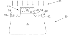
Fig. 1 shows well known semiconductor device 30, and it includes silicon substrate 32, on silicon substrate 32, is provided with the dielectric that is formed by gate oxide 34, on gate oxide 34, then is provided with polysilicon layer 36 successively.Fig. 2 shows the process 38 of carrying out that ion is implanted.For instance; We then utilize boron our arsenic capable of using of N type device or P type device; So (utilize polysilicon layer 36 and oxide 34) within the ion 39 implantable silicon substrates 32, make the polysilicon layer 36 and the zone 40,42 of silicon substrate 32 form slight doped as overall mask 41.For instance, with regard to N type device, the energy level that alloy arsenic can 3keV, 1e15/cm
2Accurate implantation the in dosage position; With regard to P type device, the energy level that dopant boron can 4keV, 2.5e14/cm
2Accurate implantation the in dosage position.Afterwards, Fig. 3 shows that oxide layer 44 is deposited on the structure of completion, and the etching that this oxide layer 44 receives anisotropic forms sept 46,48 with the both sides at polysilicon layer 36, and is as shown in Figure 4.
Fig. 4 also shows another implantation step 50.Once more for instance; We then utilize boron our arsenic capable of using of N type device or P type device; So (utilizing polysilicon layer 36, gate oxide 34 and sept 46,48) and in polysilicon body, form severe doped 52,54 within the ion 39 implantable silicon substrates 32 as overall mask 51.For instance, with regard to N type device, the energy level that alloy arsenic can 30keV, 4e15/cm
2Accurate implantation the in dosage position; With regard to P type device, the energy level that dopant boron can 3.5keV, 2e15/cm
2Accurate implantation the in dosage position.
After implant forming, for instance, we can actively anneal at 1050 ℃ (like rapid thermal annealing, rapid thermal anneal) 30 seconds, form the source region 56 and drain region 58 of device 30 to order about implant.
Next, as shown in Figure 5, metal level 60 (for example nickel) is deposited on the structure (being that polysilicon layer 36, sept 46,48, position are in source region on the silicon substrate 32 56 and drain region 58) of completion.Then, for instance, the structure of completion is carried out rapid thermal annealing at 500 ℃, causes the nickel 60 and the silicon generation reaction of polysilicon layer 36 and silicon substrate 32 to get into the nickle silicide 62,64,66 of polysilicon layer 36 and entering source region 56 and drain region 58 with generation.Thickness compared to polysilicon layer 36; Nickel dam 60 is enough thick; And the silicide step long enough of experience; With silication that whole haply polysilicon layer 36 is provided (because in this process, the wear rate of polysilicon layer 36 approximately is the twice of nickel dam 60, so nickel dam 60 thickness that we preferably select are the over half of polysilicon layer 36 thickness.For instance, be the polysilicon layer 36 of 700 dusts for thickness, we preferably select thickness to surpass the nickel dam 60 of 350 dusts.) this step forms nickel silicide gate 62, and the silicification nickel area 64,66 in source region 56 and the drain region 58.Unreacted then nickel partly is removed, and stays the structure among Fig. 6.
We will see that in silicide step metal gates 62 sees through the full consumption of polysilicon layer 36 and forms.So, we overcome above-mentioned problem about polysilicon gate.Just, compared to polysilicon gate, the conductivity of grid is improved, and we also avoid the problem of depletion of polysilicon and boron penetration.
In this silicatization process; Previous in polysilicon layer 36 alloy 39 in the equally distributed haply polysilicon layer 36 (in above-mentioned example: be arsenic in the N type device; Be boron in the P type device); Nickle silicide and polysilicon body interface through advancing downwards receive driving down; Among the alloy 39 of substantial amount was positioned at grid 62 positions 68 that are adjacent to gate oxide 34, grid 62 positions 68 that so are adjacent to gate oxide 34 were than containing higher in fact concentration of dopant away from the grid position 70 of gate oxide 34.Shovel snow (snowplowing) phenomenon of above-mentioned alloy 39 causes unexpected synthetic gate work-function.For instance, in the occasion of N type device, alloy 39 is an arsenic, and through above-mentioned steps, the synthetic gate work-function of grid 62 is 4.35eV to 4.4eV, and the gate work-function of polysilicon gate has only 4.15eV in comparison.With regard to identical device limit voltage, the work function increase in the N type device makes the concentration of dopant position standard in the device channel descend.Borrowing the decline position of concentration of dopant in the channel accurate, we can guarantee that suitable transistor closes, the current drives of avoiding above-mentioned minimizing simultaneously and the problems of not wanting such as wearing the tunnel electric current to channel that drains.
In like manner, in the occasion of P type device, alloy 39 is a boron, and through above-mentioned steps, the synthetic gate work-function of grid 62 is 4.9eV, and the work function of polysilicon gate then is 5.05eV in comparison.With regard to identical device limit voltage, the work function in the P type device reduces the concentration of dopant position standard that makes in the device channel and descends, and overcomes the problems referred to above.
Accomplish after this process, we recognize: can for example depend on the kenel of the kenel of alloy, the concentration of alloy (or shortage of alloy), metal level, and/or the step of silicatization process according to the work function that needs to select various synthetic grids.These parameters of suitable choice, we can be according to revising synthetic gate work-function.
Fig. 7 to 14 shows the second embodiment of the present invention.Fig. 7 shows a semiconductor device 80, and it comprises silicon substrate 82, which is provided with the dielectric that is formed by oxide layer 84, and is located at the polysilicon layer 86 (being thin than person shown in the process of Fig. 1 to 6 in fact) on the oxide layer 84.We are with alloy 89 implantation (88) polysilicon layers 86 of predetermined pattern and concentration (it can differ from and be about to implant the source electrode and the pattern and the concentration of drain region to form device), or polysilicon layer are not carried out doping.The selection of alloy and concentration (or selecting the shortcoming alloy) are helpful for the gate work-function of the composite structure that decision is narrated subsequently.
Mask layer (for example nitration case 90) is formed on the polysilicon layer 86, and polysilicon layer 86, cap layer 90 and gate oxide level 84 (Fig. 8) are to form with well known method.
Then; Carry out ion implantation step 92 (Fig. 9) to form slight doped 94,96; Be directed to device kenel to be made; Select suitable doping thing 98 (for example: be arsenic in the N type device, or be boron in the P type device), utilize cap layer 90, polysilicon layer 86 and gate oxide level 84 as overall mask 100.With reference to Figure 10, oxide layer 102 is deposited on the composite structure, and receives anisotropic etching with the opposite side formation sept 104,106 (among Figure 11) at polysilicon layer 86 and cap layer 90.Then; Along utilizing sept 104,106 to carry out ion implantation step 108 as cap layer 90, polysilicon layer 86 and the gate oxide level 84 of overall mask 110; To form severe doped 112,114, be directed to device kenel to be made once more, select this alloy 98 (for example to be arsenic in the N type device; Or be boron in the P type device), shown in figure 11.
Anneal (like rapid thermal annealing), activate and implant to form the source electrode and the drain region 116,118 of device 80.With reference to Figure 12, we utilize suitable means (for example etching) to remove cap layer 90 (as stated, cap layer 90 can be a material different with sept 104,106, so removing of cap layer 90 can not influence sept 104,106).
With reference to Figure 13; Next, metal level 120 (for example nickel) is deposited on the composite structure, promptly is deposited on the polysilicon layer 86; 82 of sept 104,106 and base materials are covered with source region 116 and drain region 118, and nickel dam 120 width are half the greater than polysilicon layer 86 width.
Then, composite structure experience rapid thermal annealing causes the nickel 120 and the silicon generation of polysilicon layer 86 and silicon substrate 82 to react the nickle silicide 122,124,126 that gets into polysilicon layer 86 (to form grid 122) and entering source region 116 and drain region 118 to generate.Once more, compared to the thickness of polysilicon layer 86, nickel dam 120 is enough thick, and the silicide step long enough of experience, so that the silication of whole haply polysilicon layer 86 to be provided.Yet; Polysilicon layer 86 is thin than the polysilicon layer among the embodiment shown in Fig. 1 to 6 36 in fact; So the silicide regions 124,126 in synthetic silicide grid 122 and source region 116 and the drain region 118 is thin or shallow than the counterpart among the embodiment shown in Fig. 1 to 6 in fact; Be that the degree of depth in silicide regions 124,126 entering source regions 116 and the drain region 118 is dark not as person shown in first embodiment, so avoid the not enough possible problem in source region and/or drain region.So, even source electrode and drain region are quite shallow, we also can reach the proper device framework.During ion implantation step 108 (Figure 11), on polysilicon layer 86, adding cap layer 90 can provide thin polysilicon layer 86, guarantees that simultaneously semiconductor body 82 can reach suitable shading (masking) for 110 times in overall mask.
Be similar to previous process; Previous in polysilicon layer 86 alloy 89 in the equally distributed haply polysilicon layer 86; Nickle silicide and polysilicon interface through advancing downwards receive driving down; Till among the alloy of substantial amount 89 advances grid 122 positions 150 that are adjacent to gate oxide level 84, grid 122 positions 150 that so are adjacent to gate oxide level 84 are than containing higher in fact concentration of dopant away from the grid position 152 of gate oxide level 84.Grid 122 work functions that so cause above-mentioned decision.Yet in the present embodiment, grid 122 work functions are not to depend on the source electrode 116 that is used for device 80 and the alloy 98 of drain electrode 118, but depend on the independent alloy of selecting 89 in polysilicon layer 86.Therefore, we recognize: can select and revise the work function of grid 122 according to particular demands, and have nothing to do for installing the alloy that 80 source electrode and drain electrode select.
Remove unreacted nickel part then, stay the structure among Figure 14.
We recognize: except above-mentioned specific N type and P type alloy, any other suitable doping thing, comprise N type, P type or neither the also non-P type person of N type all can effectively utilize.
At first, we recognize the advantage that is provided with metal level, promptly have higher conductivity compared to the polysilicon gate device, and avoid exhausting and problem such as penetrating of polysilicon.In addition, we can revise the work function of grid, need not on the performance of device, to compromise, and can reduce the concentration of dopant in the device channel (having its attendant advantages).
For the purpose of diagram and explanation, we are described in detail embodiments of the invention as above.We not desire the present invention is limited to above detailed content.Under above-mentioned announcement inspired, we can make other correction or variation.
To principle of the present invention and practical application thereof best explanation is provided at this selected and described embodiment, so those skilled in the art can to various execution modes and be suitable for specific use under considering various modifications and use the present invention.These all modifications and variation are in by the scope of the present invention that appending claims determined, and these claims are done the most extensively explanation of scope according to fair, legal, equivalent principle.
Claims (3)
1. method of making semiconductor structure is characterized in that:
Base material (82) is provided;
Dielectric (84) is provided on this base material (82);
Polysilicon body (86) is provided on this dielectric (84), and this polysilicon body (86) contains alloy (89);
Cap layer (90) is provided on this polysilicon body (86);
, as light shield another kind of alloy (98) is imported within this base material (82) with this cap layer (90) and this polysilicon body (86);
Remove this cap layer (90) from this polysilicon body (86);
Metal level (120) is provided on this polysilicon body (86);
The experience silicatization process forms grid (122) on whole this polysilicon body (86), to carry out silication in fact to go up at this dielectric (84); And
In this polysilicon body (86), select alloy (89), the required work function of this grid (122) is depended in the selection of this alloy.
2. the method for claim 1; It is further characterized in that in the two opposite sides of this cap layer (90) and this polysilicon body (86) and is provided with sept (104,106) that this sept (104,106) serves as light shield importing within this base material (82) by another kind alloy (98) along this cap layer (90) and this polysilicon body (86).
3. the method for claim 1, it further is characterized as this step that metal level (120) is provided and provides the nickel dam above this polysilicon body (86) thickness one half thickness on this polysilicon body.
Applications Claiming Priority (2)
| Application Number | Priority Date | Filing Date | Title |
|---|---|---|---|
| US10/135,227 US6599831B1 (en) | 2002-04-30 | 2002-04-30 | Metal gate electrode using silicidation and method of formation thereof |
| US10/135,227 | 2002-04-30 |
Related Parent Applications (1)
| Application Number | Title | Priority Date | Filing Date |
|---|---|---|---|
| CNA038097842A Division CN1729576A (en) | 2002-04-30 | 2003-04-28 | Metal gate electrode using silicidation and method of formation thereof |
Publications (2)
| Publication Number | Publication Date |
|---|---|
| CN102157362A CN102157362A (en) | 2011-08-17 |
| CN102157362B true CN102157362B (en) | 2012-05-16 |
Family
ID=27610948
Family Applications (2)
| Application Number | Title | Priority Date | Filing Date |
|---|---|---|---|
| CN2011100472901A Expired - Lifetime CN102157362B (en) | 2002-04-30 | 2003-04-28 | Metal gate electrode using silicidation and method of formation thereof |
| CNA038097842A Pending CN1729576A (en) | 2002-04-30 | 2003-04-28 | Metal gate electrode using silicidation and method of formation thereof |
Family Applications After (1)
| Application Number | Title | Priority Date | Filing Date |
|---|---|---|---|
| CNA038097842A Pending CN1729576A (en) | 2002-04-30 | 2003-04-28 | Metal gate electrode using silicidation and method of formation thereof |
Country Status (8)
| Country | Link |
|---|---|
| US (2) | US6599831B1 (en) |
| EP (1) | EP1502305A1 (en) |
| JP (1) | JP2005524243A (en) |
| KR (1) | KR20040102187A (en) |
| CN (2) | CN102157362B (en) |
| AU (1) | AU2003231119A1 (en) |
| TW (1) | TWI270935B (en) |
| WO (1) | WO2003094243A1 (en) |
Families Citing this family (35)
| Publication number | Priority date | Publication date | Assignee | Title |
|---|---|---|---|---|
| US6599831B1 (en) * | 2002-04-30 | 2003-07-29 | Advanced Micro Devices, Inc. | Metal gate electrode using silicidation and method of formation thereof |
| US7183182B2 (en) * | 2003-09-24 | 2007-02-27 | International Business Machines Corporation | Method and apparatus for fabricating CMOS field effect transistors |
| JP4011024B2 (en) * | 2004-01-30 | 2007-11-21 | 株式会社ルネサステクノロジ | Semiconductor device and manufacturing method thereof |
| JP4521597B2 (en) * | 2004-02-10 | 2010-08-11 | ルネサスエレクトロニクス株式会社 | Semiconductor memory device and manufacturing method thereof |
| US7056782B2 (en) * | 2004-02-25 | 2006-06-06 | International Business Machines Corporation | CMOS silicide metal gate integration |
| JP3998665B2 (en) * | 2004-06-16 | 2007-10-31 | 株式会社ルネサステクノロジ | Semiconductor device and manufacturing method thereof |
| JP2006013270A (en) * | 2004-06-29 | 2006-01-12 | Renesas Technology Corp | Semiconductor device and its manufacturing method |
| KR100558011B1 (en) * | 2004-07-12 | 2006-03-06 | 삼성전자주식회사 | Method of forming a MOS transistor having fully silicided metal gate electrode |
| JP2006108355A (en) * | 2004-10-05 | 2006-04-20 | Renesas Technology Corp | Semiconductor device and manufacturing method thereof |
| KR100593452B1 (en) * | 2005-02-01 | 2006-06-28 | 삼성전자주식회사 | Method of forming a mos transistor having fully silicided metal gate electrode |
| JP2006245417A (en) * | 2005-03-04 | 2006-09-14 | Toshiba Corp | Semiconductor device and manufacturing method therefor |
| WO2006098369A1 (en) * | 2005-03-15 | 2006-09-21 | Nec Corporation | Method for manufacturing semiconductor device and semiconductor device |
| US20060258074A1 (en) * | 2005-05-12 | 2006-11-16 | Texas Instruments Incorporated | Methods that mitigate excessive source/drain silicidation in full gate silicidation metal gate flows |
| JP2006339324A (en) * | 2005-06-01 | 2006-12-14 | Fujitsu Ltd | Manufacturing method of semiconductor device |
| JP2006339441A (en) * | 2005-06-02 | 2006-12-14 | Fujitsu Ltd | Manufacturing method of semiconductor device |
| EP1744351A3 (en) * | 2005-07-11 | 2008-11-26 | Interuniversitair Microelektronica Centrum ( Imec) | Method for forming a fully silicided gate MOSFET and devices obtained thereof |
| JP2007027727A (en) * | 2005-07-11 | 2007-02-01 | Interuniv Micro Electronica Centrum Vzw | Formation method for full-silicified gate mosfet and device obtained by the same method |
| KR100646937B1 (en) | 2005-08-22 | 2006-11-23 | 삼성에스디아이 주식회사 | Poly silicon thin film transistor and method for fabricating the same |
| JP2007173347A (en) * | 2005-12-20 | 2007-07-05 | Renesas Technology Corp | Semiconductor device and its manufacturing method |
| CN101356639B (en) * | 2006-01-06 | 2010-12-08 | 日本电气株式会社 | Semiconductor device and process for producing the same |
| JP2007251030A (en) * | 2006-03-17 | 2007-09-27 | Renesas Technology Corp | Semiconductor device and method of manufacturing the same |
| US7491643B2 (en) * | 2006-05-24 | 2009-02-17 | International Business Machines Corporation | Method and structure for reducing contact resistance between silicide contact and overlying metallization |
| US7297618B1 (en) | 2006-07-28 | 2007-11-20 | International Business Machines Corporation | Fully silicided gate electrodes and method of making the same |
| CN101517732B (en) * | 2006-09-20 | 2011-04-06 | 日本电气株式会社 | Semiconductor device and method for manufacturing same |
| WO2008065908A1 (en) * | 2006-11-29 | 2008-06-05 | Phyzchemix Corporation | Method for forming group iv metallic element compound film and method for manufacturing semiconductor device |
| US7727842B2 (en) * | 2007-04-27 | 2010-06-01 | Texas Instruments Incorporated | Method of simultaneously siliciding a polysilicon gate and source/drain of a semiconductor device, and related device |
| US8183137B2 (en) * | 2007-05-23 | 2012-05-22 | Texas Instruments Incorporated | Use of dopants to provide low defect gate full silicidation |
| JP2009026997A (en) * | 2007-07-20 | 2009-02-05 | Renesas Technology Corp | Semiconductor device, and manufacturing method thereof |
| US7642153B2 (en) * | 2007-10-23 | 2010-01-05 | Texas Instruments Incorporated | Methods for forming gate electrodes for integrated circuits |
| WO2009122345A1 (en) * | 2008-04-02 | 2009-10-08 | Nxp B.V. | Method of manufacturing a semiconductor device and semiconductor device |
| CN101562131B (en) * | 2008-04-15 | 2012-04-18 | 和舰科技(苏州)有限公司 | Method for manufacturing gate structure |
| US8012817B2 (en) | 2008-09-26 | 2011-09-06 | Taiwan Semiconductor Manufacturing Company, Ltd. | Transistor performance improving method with metal gate |
| US9871035B2 (en) * | 2013-12-31 | 2018-01-16 | Taiwan Semiconductor Manufacturing Co., Ltd. | Semiconductor device with metal silicide blocking region and method of manufacturing the same |
| US9972694B2 (en) * | 2015-10-20 | 2018-05-15 | Taiwan Semiconductor Manufacturing Company, Ltd. | Atomic layer deposition methods and structures thereof |
| KR102612404B1 (en) * | 2019-03-08 | 2023-12-13 | 삼성전자주식회사 | Semiconductor device and method for manufacturing the same |
Citations (3)
| Publication number | Priority date | Publication date | Assignee | Title |
|---|---|---|---|---|
| US5397909A (en) * | 1990-10-12 | 1995-03-14 | Texas Instruments Incorporated | High-performance insulated-gate field-effect transistor |
| US6228724B1 (en) * | 1999-01-28 | 2001-05-08 | Advanced Mirco Devices | Method of making high performance MOSFET with enhanced gate oxide integration and device formed thereby |
| US6281559B1 (en) * | 1999-03-03 | 2001-08-28 | Advanced Micro Devices, Inc. | Gate stack structure for variable threshold voltage |
Family Cites Families (24)
| Publication number | Priority date | Publication date | Assignee | Title |
|---|---|---|---|---|
| NL7510903A (en) * | 1975-09-17 | 1977-03-21 | Philips Nv | PROCESS FOR MANUFACTURING A SEMI-GUIDE DEVICE, AND DEVICE MANUFACTURED ACCORDING TO THE PROCESS. |
| JPS59125650A (en) * | 1983-01-07 | 1984-07-20 | Toshiba Corp | Semiconductor device and manufacture thereof |
| US4450620A (en) * | 1983-02-18 | 1984-05-29 | Bell Telephone Laboratories, Incorporated | Fabrication of MOS integrated circuit devices |
| JPS616867A (en) * | 1984-06-20 | 1986-01-13 | Nippon Telegr & Teleph Corp <Ntt> | Manufacture of semiconductor device |
| US4755865A (en) * | 1986-01-21 | 1988-07-05 | Motorola Inc. | Means for stabilizing polycrystalline semiconductor layers |
| US4746964A (en) * | 1986-08-28 | 1988-05-24 | Fairchild Semiconductor Corporation | Modification of properties of p-type dopants with other p-type dopants |
| US5237196A (en) * | 1987-04-14 | 1993-08-17 | Kabushiki Kaisha Toshiba | Semiconductor device and method for manufacturing the same |
| JPH01243549A (en) * | 1988-03-25 | 1989-09-28 | Seiko Epson Corp | Semiconductor device |
| US5767558A (en) * | 1996-05-10 | 1998-06-16 | Integrated Device Technology, Inc. | Structures for preventing gate oxide degradation |
| US6335280B1 (en) * | 1997-01-13 | 2002-01-01 | Asm America, Inc. | Tungsten silicide deposition process |
| US5851891A (en) * | 1997-04-21 | 1998-12-22 | Advanced Micro Devices, Inc. | IGFET method of forming with silicide contact on ultra-thin gate |
| US6117761A (en) * | 1997-08-23 | 2000-09-12 | Micron Technology, Inc. | Self-aligned silicide strap connection of polysilicon layers |
| US5937319A (en) * | 1997-10-31 | 1999-08-10 | Advanced Micro Devices, Inc. | Method of making a metal oxide semiconductor (MOS) transistor polysilicon gate with a size beyond photolithography limitation by using polysilicidation and selective etching |
| JPH11284179A (en) * | 1998-03-30 | 1999-10-15 | Sony Corp | Semiconductor device and manufacture thereof |
| US6091123A (en) * | 1998-06-08 | 2000-07-18 | Advanced Micro Devices | Self-aligned SOI device with body contact and NiSi2 gate |
| US6100173A (en) * | 1998-07-15 | 2000-08-08 | Advanced Micro Devices, Inc. | Forming a self-aligned silicide gate conductor to a greater thickness than junction silicide structures using a dual-salicidation process |
| US6451644B1 (en) * | 1998-11-06 | 2002-09-17 | Advanced Micro Devices, Inc. | Method of providing a gate conductor with high dopant activation |
| JP2000252462A (en) * | 1999-03-01 | 2000-09-14 | Toshiba Corp | Mis semiconductor device and manufacture thereof |
| US6245692B1 (en) * | 1999-11-23 | 2001-06-12 | Agere Systems Guardian Corp. | Method to selectively heat semiconductor wafers |
| US6365481B1 (en) * | 2000-09-13 | 2002-04-02 | Advanced Micro Devices, Inc. | Isotropic resistor protect etch to aid in residue removal |
| US6562718B1 (en) * | 2000-12-06 | 2003-05-13 | Advanced Micro Devices, Inc. | Process for forming fully silicided gates |
| US6479383B1 (en) * | 2002-02-05 | 2002-11-12 | Chartered Semiconductor Manufacturing Ltd | Method for selective removal of unreacted metal after silicidation |
| US6599831B1 (en) * | 2002-04-30 | 2003-07-29 | Advanced Micro Devices, Inc. | Metal gate electrode using silicidation and method of formation thereof |
| US6544829B1 (en) * | 2002-09-20 | 2003-04-08 | Lsi Logic Corporation | Polysilicon gate salicidation |
-
2002
- 2002-04-30 US US10/135,227 patent/US6599831B1/en not_active Expired - Lifetime
-
2003
- 2003-04-28 KR KR10-2004-7017334A patent/KR20040102187A/en active Search and Examination
- 2003-04-28 AU AU2003231119A patent/AU2003231119A1/en not_active Abandoned
- 2003-04-28 JP JP2004502363A patent/JP2005524243A/en active Pending
- 2003-04-28 WO PCT/US2003/012958 patent/WO2003094243A1/en active Application Filing
- 2003-04-28 EP EP03724248A patent/EP1502305A1/en not_active Withdrawn
- 2003-04-28 CN CN2011100472901A patent/CN102157362B/en not_active Expired - Lifetime
- 2003-04-28 CN CNA038097842A patent/CN1729576A/en active Pending
- 2003-04-30 TW TW092110111A patent/TWI270935B/en not_active IP Right Cessation
- 2003-05-07 US US10/431,008 patent/US6873030B2/en not_active Expired - Lifetime
Patent Citations (3)
| Publication number | Priority date | Publication date | Assignee | Title |
|---|---|---|---|---|
| US5397909A (en) * | 1990-10-12 | 1995-03-14 | Texas Instruments Incorporated | High-performance insulated-gate field-effect transistor |
| US6228724B1 (en) * | 1999-01-28 | 2001-05-08 | Advanced Mirco Devices | Method of making high performance MOSFET with enhanced gate oxide integration and device formed thereby |
| US6281559B1 (en) * | 1999-03-03 | 2001-08-28 | Advanced Micro Devices, Inc. | Gate stack structure for variable threshold voltage |
Also Published As
| Publication number | Publication date |
|---|---|
| TWI270935B (en) | 2007-01-11 |
| JP2005524243A (en) | 2005-08-11 |
| US6599831B1 (en) | 2003-07-29 |
| US6873030B2 (en) | 2005-03-29 |
| US20030203609A1 (en) | 2003-10-30 |
| CN102157362A (en) | 2011-08-17 |
| EP1502305A1 (en) | 2005-02-02 |
| WO2003094243A1 (en) | 2003-11-13 |
| KR20040102187A (en) | 2004-12-03 |
| CN1729576A (en) | 2006-02-01 |
| AU2003231119A1 (en) | 2003-11-17 |
| TW200403729A (en) | 2004-03-01 |
Similar Documents
| Publication | Publication Date | Title |
|---|---|---|
| CN102157362B (en) | Metal gate electrode using silicidation and method of formation thereof | |
| JP3495869B2 (en) | Method for manufacturing semiconductor device | |
| US5514889A (en) | Non-volatile semiconductor memory device and method for manufacturing the same | |
| US6482698B2 (en) | Method of manufacturing an electrically programmable, non-volatile memory and high-performance logic circuitry in the same semiconductor chip | |
| US5292681A (en) | Method of processing a semiconductor wafer to form an array of nonvolatile memory devices employing floating gate transistors and peripheral area having CMOS transistors | |
| JPH06268165A (en) | Preparation of semiconductor transistor and its structure | |
| US20060273391A1 (en) | CMOS devices for low power integrated circuits | |
| EP0390509B1 (en) | Semi-conductor device and method of manufacturing the same | |
| US5627087A (en) | Process for fabricating metal-oxide semiconductor (MOS) transistors based on lightly doped drain (LDD) structure | |
| JP4846167B2 (en) | Manufacturing method of semiconductor device | |
| WO1998044552A9 (en) | Method of manufacturing a non-volatile memory combining an eprom with a standard cmos process | |
| WO1998044552A2 (en) | Method of manufacturing a non-volatile memory combining an eprom with a standard cmos process | |
| KR100657823B1 (en) | Semiconductor device with recessed gate and method for manufacturing the same | |
| US20060141712A1 (en) | Method for manufacturing PMOSFET | |
| TWI277174B (en) | Semiconductor device having different metal silicide portions and method for fabricating the semiconductor device | |
| EP1102319B1 (en) | Process for manufacturing electronic devices comprising high-voltage MOS and EEPROM transistors | |
| JP2003332461A (en) | Method of manufacturing semiconductor element including triple well structure | |
| KR100733703B1 (en) | Semiconductor device and method of manufactruing the same | |
| JP3120428B2 (en) | Method for manufacturing MOS type semiconductor device | |
| JP2808620B2 (en) | Method for manufacturing semiconductor device | |
| KR100506269B1 (en) | Well Forming Method of Semiconductor Device | |
| JP2860483B2 (en) | Method for manufacturing semiconductor device | |
| TW552703B (en) | Manufacturing method of mask ROM | |
| KR100745930B1 (en) | Method for manufacturing semiconductor device | |
| JP2002057222A (en) | Semiconductor device and its manufacturing method |
Legal Events
| Date | Code | Title | Description |
|---|---|---|---|
| C06 | Publication | ||
| PB01 | Publication | ||
| C10 | Entry into substantive examination | ||
| SE01 | Entry into force of request for substantive examination | ||
| C14 | Grant of patent or utility model | ||
| GR01 | Patent grant | ||
| CX01 | Expiry of patent term |
Granted publication date: 20120516 |
|
| CX01 | Expiry of patent term |