CN102187455B - Method of making split gate memory cell - Google Patents
Method of making split gate memory cell Download PDFInfo
- Publication number
- CN102187455B CN102187455B CN200980141501.9A CN200980141501A CN102187455B CN 102187455 B CN102187455 B CN 102187455B CN 200980141501 A CN200980141501 A CN 200980141501A CN 102187455 B CN102187455 B CN 102187455B
- Authority
- CN
- China
- Prior art keywords
- layer
- grid material
- mask layer
- hard mask
- grid
- Prior art date
- Legal status (The legal status is an assumption and is not a legal conclusion. Google has not performed a legal analysis and makes no representation as to the accuracy of the status listed.)
- Active
Links
- 238000004519 manufacturing process Methods 0.000 title description 3
- 239000000463 material Substances 0.000 claims abstract description 113
- 238000000034 method Methods 0.000 claims abstract description 62
- 239000004065 semiconductor Substances 0.000 claims abstract description 27
- 239000000758 substrate Substances 0.000 claims abstract description 12
- 150000004767 nitrides Chemical group 0.000 claims description 22
- 239000002159 nanocrystal Substances 0.000 claims description 10
- 238000005498 polishing Methods 0.000 claims description 7
- 230000000717 retained effect Effects 0.000 claims 2
- 230000000873 masking effect Effects 0.000 abstract 3
- 229910021420 polycrystalline silicon Inorganic materials 0.000 description 32
- 229920005591 polysilicon Polymers 0.000 description 32
- 238000005530 etching Methods 0.000 description 16
- 229920002120 photoresistant polymer Polymers 0.000 description 11
- 230000009471 action Effects 0.000 description 10
- 239000000126 substance Substances 0.000 description 10
- 125000006850 spacer group Chemical group 0.000 description 8
- NBIIXXVUZAFLBC-UHFFFAOYSA-N Phosphoric acid Chemical compound OP(O)(O)=O NBIIXXVUZAFLBC-UHFFFAOYSA-N 0.000 description 4
- 230000008901 benefit Effects 0.000 description 3
- 238000000059 patterning Methods 0.000 description 3
- XUIMIQQOPSSXEZ-UHFFFAOYSA-N Silicon Chemical compound [Si] XUIMIQQOPSSXEZ-UHFFFAOYSA-N 0.000 description 2
- 229910000147 aluminium phosphate Inorganic materials 0.000 description 2
- 210000000988 bone and bone Anatomy 0.000 description 2
- 230000008859 change Effects 0.000 description 2
- 230000006870 function Effects 0.000 description 2
- 229910052751 metal Inorganic materials 0.000 description 2
- 239000002184 metal Substances 0.000 description 2
- 238000012986 modification Methods 0.000 description 2
- 230000004048 modification Effects 0.000 description 2
- 229910052710 silicon Inorganic materials 0.000 description 2
- 239000010703 silicon Substances 0.000 description 2
- ZAMOUSCENKQFHK-UHFFFAOYSA-N Chlorine atom Chemical compound [Cl] ZAMOUSCENKQFHK-UHFFFAOYSA-N 0.000 description 1
- 229910001218 Gallium arsenide Inorganic materials 0.000 description 1
- OAICVXFJPJFONN-UHFFFAOYSA-N Phosphorus Chemical compound [P] OAICVXFJPJFONN-UHFFFAOYSA-N 0.000 description 1
- 229910000577 Silicon-germanium Inorganic materials 0.000 description 1
- 238000009825 accumulation Methods 0.000 description 1
- 229910052785 arsenic Inorganic materials 0.000 description 1
- RQNWIZPPADIBDY-UHFFFAOYSA-N arsenic atom Chemical compound [As] RQNWIZPPADIBDY-UHFFFAOYSA-N 0.000 description 1
- 230000015572 biosynthetic process Effects 0.000 description 1
- 239000003795 chemical substances by application Substances 0.000 description 1
- 239000000460 chlorine Substances 0.000 description 1
- 229910052801 chlorine Inorganic materials 0.000 description 1
- 239000011248 coating agent Substances 0.000 description 1
- 238000000576 coating method Methods 0.000 description 1
- 239000004020 conductor Substances 0.000 description 1
- 238000005260 corrosion Methods 0.000 description 1
- 230000007797 corrosion Effects 0.000 description 1
- 230000008021 deposition Effects 0.000 description 1
- 239000003989 dielectric material Substances 0.000 description 1
- 239000002019 doping agent Substances 0.000 description 1
- 238000002347 injection Methods 0.000 description 1
- 239000007924 injection Substances 0.000 description 1
- 239000012212 insulator Substances 0.000 description 1
- 229910021421 monocrystalline silicon Inorganic materials 0.000 description 1
- 229910052698 phosphorus Inorganic materials 0.000 description 1
- 239000011574 phosphorus Substances 0.000 description 1
- 238000001020 plasma etching Methods 0.000 description 1
- 238000012913 prioritisation Methods 0.000 description 1
- 239000000243 solution Substances 0.000 description 1
- 238000001039 wet etching Methods 0.000 description 1
Images


Classifications
-
- B—PERFORMING OPERATIONS; TRANSPORTING
- B82—NANOTECHNOLOGY
- B82Y—SPECIFIC USES OR APPLICATIONS OF NANOSTRUCTURES; MEASUREMENT OR ANALYSIS OF NANOSTRUCTURES; MANUFACTURE OR TREATMENT OF NANOSTRUCTURES
- B82Y10/00—Nanotechnology for information processing, storage or transmission, e.g. quantum computing or single electron logic
-
- H—ELECTRICITY
- H01—ELECTRIC ELEMENTS
- H01L—SEMICONDUCTOR DEVICES NOT COVERED BY CLASS H10
- H01L21/00—Processes or apparatus adapted for the manufacture or treatment of semiconductor or solid state devices or of parts thereof
- H01L21/02—Manufacture or treatment of semiconductor devices or of parts thereof
- H01L21/04—Manufacture or treatment of semiconductor devices or of parts thereof the devices having at least one potential-jump barrier or surface barrier, e.g. PN junction, depletion layer or carrier concentration layer
- H01L21/18—Manufacture or treatment of semiconductor devices or of parts thereof the devices having at least one potential-jump barrier or surface barrier, e.g. PN junction, depletion layer or carrier concentration layer the devices having semiconductor bodies comprising elements of Group IV of the Periodic System or AIIIBV compounds with or without impurities, e.g. doping materials
- H01L21/30—Treatment of semiconductor bodies using processes or apparatus not provided for in groups H01L21/20 - H01L21/26
- H01L21/31—Treatment of semiconductor bodies using processes or apparatus not provided for in groups H01L21/20 - H01L21/26 to form insulating layers thereon, e.g. for masking or by using photolithographic techniques; After treatment of these layers; Selection of materials for these layers
- H01L21/3105—After-treatment
- H01L21/31051—Planarisation of the insulating layers
-
- H—ELECTRICITY
- H01—ELECTRIC ELEMENTS
- H01L—SEMICONDUCTOR DEVICES NOT COVERED BY CLASS H10
- H01L29/00—Semiconductor devices adapted for rectifying, amplifying, oscillating or switching, or capacitors or resistors with at least one potential-jump barrier or surface barrier, e.g. PN junction depletion layer or carrier concentration layer; Details of semiconductor bodies or of electrodes thereof ; Multistep manufacturing processes therefor
- H01L29/40—Electrodes ; Multistep manufacturing processes therefor
- H01L29/401—Multistep manufacturing processes
- H01L29/4011—Multistep manufacturing processes for data storage electrodes
- H01L29/40114—Multistep manufacturing processes for data storage electrodes the electrodes comprising a conductor-insulator-conductor-insulator-semiconductor structure
-
- H—ELECTRICITY
- H01—ELECTRIC ELEMENTS
- H01L—SEMICONDUCTOR DEVICES NOT COVERED BY CLASS H10
- H01L29/00—Semiconductor devices adapted for rectifying, amplifying, oscillating or switching, or capacitors or resistors with at least one potential-jump barrier or surface barrier, e.g. PN junction depletion layer or carrier concentration layer; Details of semiconductor bodies or of electrodes thereof ; Multistep manufacturing processes therefor
- H01L29/40—Electrodes ; Multistep manufacturing processes therefor
- H01L29/401—Multistep manufacturing processes
- H01L29/4011—Multistep manufacturing processes for data storage electrodes
- H01L29/40117—Multistep manufacturing processes for data storage electrodes the electrodes comprising a charge-trapping insulator
-
- H—ELECTRICITY
- H01—ELECTRIC ELEMENTS
- H01L—SEMICONDUCTOR DEVICES NOT COVERED BY CLASS H10
- H01L29/00—Semiconductor devices adapted for rectifying, amplifying, oscillating or switching, or capacitors or resistors with at least one potential-jump barrier or surface barrier, e.g. PN junction depletion layer or carrier concentration layer; Details of semiconductor bodies or of electrodes thereof ; Multistep manufacturing processes therefor
- H01L29/40—Electrodes ; Multistep manufacturing processes therefor
- H01L29/41—Electrodes ; Multistep manufacturing processes therefor characterised by their shape, relative sizes or dispositions
- H01L29/423—Electrodes ; Multistep manufacturing processes therefor characterised by their shape, relative sizes or dispositions not carrying the current to be rectified, amplified or switched
- H01L29/42312—Gate electrodes for field effect devices
- H01L29/42316—Gate electrodes for field effect devices for field-effect transistors
- H01L29/4232—Gate electrodes for field effect devices for field-effect transistors with insulated gate
- H01L29/42324—Gate electrodes for transistors with a floating gate
- H01L29/42328—Gate electrodes for transistors with a floating gate with at least one additional gate other than the floating gate and the control gate, e.g. program gate, erase gate or select gate
-
- H—ELECTRICITY
- H01—ELECTRIC ELEMENTS
- H01L—SEMICONDUCTOR DEVICES NOT COVERED BY CLASS H10
- H01L29/00—Semiconductor devices adapted for rectifying, amplifying, oscillating or switching, or capacitors or resistors with at least one potential-jump barrier or surface barrier, e.g. PN junction depletion layer or carrier concentration layer; Details of semiconductor bodies or of electrodes thereof ; Multistep manufacturing processes therefor
- H01L29/40—Electrodes ; Multistep manufacturing processes therefor
- H01L29/41—Electrodes ; Multistep manufacturing processes therefor characterised by their shape, relative sizes or dispositions
- H01L29/423—Electrodes ; Multistep manufacturing processes therefor characterised by their shape, relative sizes or dispositions not carrying the current to be rectified, amplified or switched
- H01L29/42312—Gate electrodes for field effect devices
- H01L29/42316—Gate electrodes for field effect devices for field-effect transistors
- H01L29/4232—Gate electrodes for field effect devices for field-effect transistors with insulated gate
- H01L29/42324—Gate electrodes for transistors with a floating gate
- H01L29/42332—Gate electrodes for transistors with a floating gate with the floating gate formed by two or more non connected parts, e.g. multi-particles flating gate
-
- H—ELECTRICITY
- H01—ELECTRIC ELEMENTS
- H01L—SEMICONDUCTOR DEVICES NOT COVERED BY CLASS H10
- H01L29/00—Semiconductor devices adapted for rectifying, amplifying, oscillating or switching, or capacitors or resistors with at least one potential-jump barrier or surface barrier, e.g. PN junction depletion layer or carrier concentration layer; Details of semiconductor bodies or of electrodes thereof ; Multistep manufacturing processes therefor
- H01L29/40—Electrodes ; Multistep manufacturing processes therefor
- H01L29/41—Electrodes ; Multistep manufacturing processes therefor characterised by their shape, relative sizes or dispositions
- H01L29/423—Electrodes ; Multistep manufacturing processes therefor characterised by their shape, relative sizes or dispositions not carrying the current to be rectified, amplified or switched
- H01L29/42312—Gate electrodes for field effect devices
- H01L29/42316—Gate electrodes for field effect devices for field-effect transistors
- H01L29/4232—Gate electrodes for field effect devices for field-effect transistors with insulated gate
- H01L29/4234—Gate electrodes for transistors with charge trapping gate insulator
- H01L29/42344—Gate electrodes for transistors with charge trapping gate insulator with at least one additional gate, e.g. program gate, erase gate or select gate
-
- H—ELECTRICITY
- H01—ELECTRIC ELEMENTS
- H01L—SEMICONDUCTOR DEVICES NOT COVERED BY CLASS H10
- H01L29/00—Semiconductor devices adapted for rectifying, amplifying, oscillating or switching, or capacitors or resistors with at least one potential-jump barrier or surface barrier, e.g. PN junction depletion layer or carrier concentration layer; Details of semiconductor bodies or of electrodes thereof ; Multistep manufacturing processes therefor
- H01L29/66—Types of semiconductor device ; Multistep manufacturing processes therefor
- H01L29/66007—Multistep manufacturing processes
- H01L29/66075—Multistep manufacturing processes of devices having semiconductor bodies comprising group 14 or group 13/15 materials
- H01L29/66227—Multistep manufacturing processes of devices having semiconductor bodies comprising group 14 or group 13/15 materials the devices being controllable only by the electric current supplied or the electric potential applied, to an electrode which does not carry the current to be rectified, amplified or switched, e.g. three-terminal devices
- H01L29/66409—Unipolar field-effect transistors
- H01L29/66477—Unipolar field-effect transistors with an insulated gate, i.e. MISFET
- H01L29/66825—Unipolar field-effect transistors with an insulated gate, i.e. MISFET with a floating gate
-
- H—ELECTRICITY
- H01—ELECTRIC ELEMENTS
- H01L—SEMICONDUCTOR DEVICES NOT COVERED BY CLASS H10
- H01L29/00—Semiconductor devices adapted for rectifying, amplifying, oscillating or switching, or capacitors or resistors with at least one potential-jump barrier or surface barrier, e.g. PN junction depletion layer or carrier concentration layer; Details of semiconductor bodies or of electrodes thereof ; Multistep manufacturing processes therefor
- H01L29/66—Types of semiconductor device ; Multistep manufacturing processes therefor
- H01L29/66007—Multistep manufacturing processes
- H01L29/66075—Multistep manufacturing processes of devices having semiconductor bodies comprising group 14 or group 13/15 materials
- H01L29/66227—Multistep manufacturing processes of devices having semiconductor bodies comprising group 14 or group 13/15 materials the devices being controllable only by the electric current supplied or the electric potential applied, to an electrode which does not carry the current to be rectified, amplified or switched, e.g. three-terminal devices
- H01L29/66409—Unipolar field-effect transistors
- H01L29/66477—Unipolar field-effect transistors with an insulated gate, i.e. MISFET
- H01L29/66833—Unipolar field-effect transistors with an insulated gate, i.e. MISFET with a charge trapping gate insulator, e.g. MNOS transistors
-
- H—ELECTRICITY
- H01—ELECTRIC ELEMENTS
- H01L—SEMICONDUCTOR DEVICES NOT COVERED BY CLASS H10
- H01L29/00—Semiconductor devices adapted for rectifying, amplifying, oscillating or switching, or capacitors or resistors with at least one potential-jump barrier or surface barrier, e.g. PN junction depletion layer or carrier concentration layer; Details of semiconductor bodies or of electrodes thereof ; Multistep manufacturing processes therefor
- H01L29/66—Types of semiconductor device ; Multistep manufacturing processes therefor
- H01L29/68—Types of semiconductor device ; Multistep manufacturing processes therefor controllable by only the electric current supplied, or only the electric potential applied, to an electrode which does not carry the current to be rectified, amplified or switched
- H01L29/76—Unipolar devices, e.g. field effect transistors
- H01L29/772—Field effect transistors
- H01L29/78—Field effect transistors with field effect produced by an insulated gate
- H01L29/788—Field effect transistors with field effect produced by an insulated gate with floating gate
- H01L29/7881—Programmable transistors with only two possible levels of programmation
-
- H—ELECTRICITY
- H01—ELECTRIC ELEMENTS
- H01L—SEMICONDUCTOR DEVICES NOT COVERED BY CLASS H10
- H01L29/00—Semiconductor devices adapted for rectifying, amplifying, oscillating or switching, or capacitors or resistors with at least one potential-jump barrier or surface barrier, e.g. PN junction depletion layer or carrier concentration layer; Details of semiconductor bodies or of electrodes thereof ; Multistep manufacturing processes therefor
- H01L29/66—Types of semiconductor device ; Multistep manufacturing processes therefor
- H01L29/68—Types of semiconductor device ; Multistep manufacturing processes therefor controllable by only the electric current supplied, or only the electric potential applied, to an electrode which does not carry the current to be rectified, amplified or switched
- H01L29/76—Unipolar devices, e.g. field effect transistors
- H01L29/772—Field effect transistors
- H01L29/78—Field effect transistors with field effect produced by an insulated gate
- H01L29/792—Field effect transistors with field effect produced by an insulated gate with charge trapping gate insulator, e.g. MNOS-memory transistors
-
- H—ELECTRICITY
- H10—SEMICONDUCTOR DEVICES; ELECTRIC SOLID-STATE DEVICES NOT OTHERWISE PROVIDED FOR
- H10B—ELECTRONIC MEMORY DEVICES
- H10B41/00—Electrically erasable-and-programmable ROM [EEPROM] devices comprising floating gates
- H10B41/40—Electrically erasable-and-programmable ROM [EEPROM] devices comprising floating gates characterised by the peripheral circuit region
- H10B41/42—Simultaneous manufacture of periphery and memory cells
- H10B41/43—Simultaneous manufacture of periphery and memory cells comprising only one type of peripheral transistor
- H10B41/44—Simultaneous manufacture of periphery and memory cells comprising only one type of peripheral transistor with a control gate layer also being used as part of the peripheral transistor
-
- H—ELECTRICITY
- H10—SEMICONDUCTOR DEVICES; ELECTRIC SOLID-STATE DEVICES NOT OTHERWISE PROVIDED FOR
- H10B—ELECTRONIC MEMORY DEVICES
- H10B41/00—Electrically erasable-and-programmable ROM [EEPROM] devices comprising floating gates
- H10B41/40—Electrically erasable-and-programmable ROM [EEPROM] devices comprising floating gates characterised by the peripheral circuit region
- H10B41/42—Simultaneous manufacture of periphery and memory cells
- H10B41/43—Simultaneous manufacture of periphery and memory cells comprising only one type of peripheral transistor
- H10B41/48—Simultaneous manufacture of periphery and memory cells comprising only one type of peripheral transistor with a tunnel dielectric layer also being used as part of the peripheral transistor
-
- H—ELECTRICITY
- H10—SEMICONDUCTOR DEVICES; ELECTRIC SOLID-STATE DEVICES NOT OTHERWISE PROVIDED FOR
- H10B—ELECTRONIC MEMORY DEVICES
- H10B43/00—EEPROM devices comprising charge-trapping gate insulators
- H10B43/40—EEPROM devices comprising charge-trapping gate insulators characterised by the peripheral circuit region
Abstract
A method includes forming a first layer of gate material (18) over a semiconductor substrate (12); forming a hard mask layer (20) over the first layer; forming an opening (22); forming a charge storage layer (24) over the hard mask layer and within the opening; forming a second layer (26) of gate material over the charge storage layer; removing a portion of the second layer and a portion of the charge storage layer which overlie the hard mask layer, wherein a second portion of the second layer remains within the opening; forming a patterned masking layer (28, 30, 32) over the hard mask layer and over the second portion, wherein the patterned masking layer defines both a first and second bitcell; ; and forming the first and second bitcell using the patterned masking layer, wherein each of the first and second bitcell comprises a select gate (38, 40) made from the first layer and a control gate (34, 36) made from the second layer.
Description
Technical field
Disclosure relate generally to semiconductor memory, more specifically, relates to and manufactures the nonvolatile memory (NVM) with splitting bar.
Background technology
Have been found that split-gate nonvolatile memory (NVM) is provided for a lot of benefits of reliable operation.Yet, processing this type of structural formula and occurring the difficulty of manufacture view.The close proximity that can be comprised two grids that the charge storage layer of nanocrystal separates is parts of problem.In addition the integrated number that increases processing step of NVM and logic transistor.
Therefore, there are the improved needs to the manufacture view of splitting bar NVM.
Accompanying drawing explanation
By accompanying drawing, in the mode of example, illustrate the present invention, and the present invention is not subject to the restriction of accompanying drawing, in the accompanying drawings, identical Reference numeral is indicated similar element.Element in figure is illustrated for simple and clear object, and not necessarily draws in proportion.
Fig. 1 be in processing according to embodiment one the stage place the cross-sectional view of device architecture;
Fig. 2 is the cross-sectional view of device architecture of the Fig. 1 at the subsequent step place in processing;
Fig. 3 is the cross-sectional view of device architecture of the Fig. 2 at the subsequent step place in processing;
Fig. 4 is the cross-sectional view of device architecture of the Fig. 3 at the subsequent step place in processing;
Fig. 5 is the cross-sectional view of device architecture of the Fig. 4 at the subsequent step place in processing;
Fig. 6 is the cross-sectional view of device architecture of the Fig. 5 at the subsequent step place in processing;
Fig. 7 is the cross-sectional view of device architecture of the Fig. 6 at the subsequent step place in processing;
Fig. 8 is the cross-sectional view of device architecture of the Fig. 7 at the subsequent step place in processing;
Fig. 9 is the cross-sectional view of device architecture of the Fig. 8 at the subsequent step place in processing;
Figure 10 is the cross-sectional view of device architecture of the Fig. 9 at the subsequent step place in processing;
Figure 11 is the cross-sectional view of device architecture of the Figure 10 at the subsequent step place in processing.
Embodiment
On the one hand, above gate-dielectric, form ground floor grid material, and above grid material, form hard mask material.In hard mask material and grid material, form opening.This opening with can comprise that the charge storage layer of nanocrystal is arranged in rows.Deposit preferably relatively thick second layer grid material and its filling opening.Eat-back (the etch back) that preferably by chemico-mechanical polishing (CMP), carried out causes the second layer to flush with the end face of residue hard mask material.The second layer can remain on this level, or even can be further etched, thereby in the height lower than ground floor grid material.The patterning etching of the second layer and ground floor forms simultaneously and selects grid, controls grid and logic gate.Subsequent treatment is removed hard mask layer, forms sidewall spacer and source/drain regions.With reference to accompanying drawing and following explanation, can understand better this point.
Semiconductor substrate as herein described can be the combination of any semi-conducting material or material, such as GaAs, SiGe, silicon-on-insulator (SOI), silicon, monocrystalline silicon etc. and above-mentioned every combination.
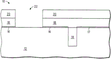
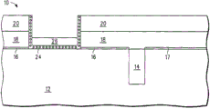
Shown in Fig. 1 is semiconductor device 10, it comprise gate dielectric layer 17 on the substrate 12 of isolated area 14 in Semiconductor substrate 12, substrate 12, the gate dielectric layer 16 on the substrate 12 of a side of isolated area 14, the side relative with gate dielectric layer 16 in isolated area, gate dielectric layer 16 and 17 and isolated area 14 on polysilicon layer 18 and the nitride layer 20 above polysilicon layer 20.Nitride layer 20 serves as hard mask, and can be another suitable material.One side with gate-dielectric 16 is to form the place of nonvolatile memory (NVM) memory cell.One side with gate-dielectric 17 is to form the place of logic transistor.Logic transistor is used for carrying out any of various logic functions, and conventionally for speed, designs.Nitride layer 20 and polysilicon layer 18 each can be about 1500 dusts thick.Can use other thickness, but nitride layer 20 should at least 500 dusts, because it is used as hard mask, and are not only antireflecting coating (ARC).Similarly, polysilicon layer 18 can be other thickness, but at least 500 dusts preferably.Gate-dielectric 16 and 17 can form simultaneously, and can be therefore identical thickness (if effectively words are useful thickness).If need different gate-dielectrics, they can have different materials or different thickness.Gate-dielectric 16 and 17 can be grown to approximately 40 dusts by heat.Gate-dielectric can change, and can have different materials and thickness.May wish to there is thin oxide layer between polysilicon layer 18 and nitride layer 20, only 80 dusts.
Shown in Fig. 2 is to form patterning etching with the semiconductor device 10 after NVM side forms opening 22 by hard mask 20, polysilicon layer 18 and gate-dielectric 16.Opening 22 is can approximately 5000 dusts wide.This is the anisotropic etching of using (by the chemical action of being filled up by reader).
Shown in Fig. 3 be in opening 22 and hard mask layer 20 above semiconductor device 10 after deposited charge accumulation layer 24.Charge storage layer 24 can be used nanocrystal to carry out charge storage.In this case, can be by first forming dielectric layer, being then that nanocrystal forms to make charge storage layer 24.Nanocrystal around and above form another dielectric layer.Another charge material such as nitride also can be implemented.Charge storage layer 24 can be thick for approximately 200 dusts.This thickness can change, if especially use large nanocrystal (approximately 100 dusts or larger some).
Shown in Fig. 4 is the semiconductor device after deposit spathic silicon layer 26 10 above charge storage layer 24.Polysilicon layer 18 and 26 (as polysilicon) is useful forming when for use as controlling the grid of grid, for use as the grid of the grid of selecting grid and grid in transistor for use as carrying out from the logic function different as NVM.May find that other material such as electric conducting material is useful.For example, making metal can be used as many work of grid aspect.Polysilicon layer 26 is preferably relatively thick, at least thick as the degree of depth of the opening 22 in Figure 12.In this case, it can be approximately 2800 dusts.In fact, preferably it is even thicker, for example approximately 5000 dusts.
Shown in Fig. 5 is chemico-mechanical polishing (CMP) polysilicon layer 26 semiconductor device 10 afterwards, and the end face of the remainder of polysilicon layer 26 is flushed with the end face of nitride layer 20.
Shown in Fig. 6 is to carry out to eat-back the height of the remainder of polysilicon layer 26 to be reduced to the following semiconductor device 10 afterwards of height of the end face of polysilicon layer 18.Use and between nitride and polysilicon, there is optionally chemical action and carry out and eat-back.This type of chemical action can be that oxide is also had optionally, makes charge storage layer 24 not by remarkable etching.The example of this type of etching is to use the reactive ion etching of the chemical action based on chlorine.This type of example is CI
2+ HBr, He+O
2and CF
4.
Deposition photoresist layer shown in Fig. 7 and by its patterning with stay photoresist part 28,30 and 32 after semiconductor device 10.A part for nitride layer 20 and a part for polysilicon layer 26 in one side of the opening that photoresist part 28 and remainder at polysilicon layer 26 reside therein are overlapping.A part for nitride layer 20 and a part for polysilicon layer 26 on the opposite side of the opening that photoresist part 30 and remainder at polysilicon layer 26 reside therein are overlapping.Photoresist part 32 is above will the transistorized logical gate of completion logic.
Shown in Fig. 8 be use photoresist part 28,30 and 32 by nitride layer 20 etch polysilicon layers 18 to leave respectively selection grid 34 and 36 and semiconductor device 10 after the remaining logic gate 42 of polysilicon layer 18 photoresist part 28,30 and 32 below.Etching is also by polysilicon layer 26 and charge storage layer 24, and it stays respectively from the remaining control grid 38 of polysilicon layer 26 and 40 below photoresist 28 and 30.This etching in three steps.First step is the etching of nitride.Second step is the etching of polysilicon.Therefore, although polysilicon 36 is thicker and polysilicon 36 is by over etching than polysilicon 40, charge storage layer 24 serves as etch stop layer.Therefore, during the period of over etching, substrate 12 is protected.Third step is by the etching of charge storage layer 24.During this etching, may there is sizable corrosion of photoresist part 28,30 and 32.For removing the etching agent of the charge storage layer of nitride, polysilicon and nanocrystal, be well-known.The example that is used for the chemical action of etch nitride layer 20 is (by the chemical action of being filled up by reader).The example that is used for the chemical action of etch polysilicon layer 18 is (by the chemical action of being filled up by reader).The example that is used for the chemical action of etching charge storage layer 24 is (by the chemical action of being filled up by reader).
Shown in Fig. 9 be remove photoresist part 28,30 and 32 and the remainder of nitride layer 20 after semiconductor device 10.During nitride etch, the vertical component of charge storage layer 24 also reduces aspect height.The wet etching of hot phosphoric acid can be used for to this etching of nitride, it has high selectivity for oxide, may wish in this case between polysilicon layer 18 and nitride layer 20, to there is previously described thin oxide layer, because hot phosphoric acid can make polysilicon become rugged.
Shown in Fig. 9 is to carry out low concentration source electrode/drain electrode to inject for the semiconductor device 10 after using when forming source/drain extension, and described source/drain extension causes forming lightly doped region 44,46,48,50 and 52.This injection can be the N-shaped dopant such as arsenic and phosphorus.
Being formed in shown in Figure 11 be illustrated as selecting sidewall spacer 54 and 58 on the side of grid 38 in cross-sectional view, select sidewall spacer 56 on the side of grid 34, select sidewall spacer 60 on the side of grid 36, select sidewall spacer 62 on the side of grid 40 and 64 and the side of logic gate 42 on sidewall spacer 68 and the semiconductor device 10 after a plurality of sidewall spacers of 70.Use sidewall spacer as mask, carry out and inject to form heavy doping source electrode/ drain region 72,74,76,78,80 and 82.
Therefore, semiconductor device 10 demonstrates the shared public doped region 56 that can be regarded as drain electrode of a bit cell.According to how utilizing when programming and wiping, selecting grid and controlling grid, in some scheme, can make source electrode and drain contrary.And the grid that two bit locations make them limits with two masks only, and in addition, in those two masks one limits the grid that logic transistor makes it.A step is the formation of opening 22.Another step is the use of the photoresist part shown in Fig. 7 and 8.
Up to the present, will be appreciated that the method that is used to form semiconductor structure is provided.The method is included in Semiconductor substrate top and forms gate dielectric layer.Described method is also included in gate dielectric layer top and forms ground floor grid material.Described method is also included in ground floor grid material top and forms hard mask layer.Described method also comprises by hard mask layer and ground floor grid material and forms opening.Described method is also included in hard mask layer top and opening and forms charge storage layer.Described method is also included in charge storage layer top and forms second layer grid material, and wherein, the thickness of second layer grid material is at least equally large with the gross thickness of ground floor grid material and hard mask layer.Described method also comprises removes the part of second layer grid material and the part of charge storage layer that covers hard mask layer, and wherein, described removal is used hard mask layer as stop layer, and wherein, the second portion of second layer grid material is still in opening.Described method is also included in above hard mask layer and above the second portion of the second layer grid material in opening and forms patterned mask layer, and wherein, described patterned mask layer limits the first bit location and second unit.Described method also comprises by patterned mask layer and forms the first bit location and second unit, wherein, each in the first bit location and second unit comprises the selection grid of being made by ground floor grid material and the control grid of being made by second layer grid material.Described method can also comprise the second portion depression of the second layer grid material making in opening, makes after this depression, and the end face of the second portion of the second layer grid material in opening is not coplanar with the end face of ground floor grid material.The feature of described method can further be to form hard mask layer above ground floor grid material, and its feature is further that hard mask layer has 500 dusts or larger thickness.The feature of described method can further be to form hard mask layer above ground floor grid material, and its feature is further that hard mask layer is nitride layer.Described method can feature can further be remove to cover part second layer grid material and the part charge storage layer of hard mask layer, its feature is further to carry out chemico-mechanical polishing to remove part second layer grid material and the part charge storage layer that covers hard mask layer.The feature of described method can further be to form patterned mask layer, and its feature is further that described patterned mask layer further limits the grid of logic transistor.Described method can also comprise the grid that forms logic transistor by patterned mask layer, and wherein, the grid of logic transistor is made by ground floor grid material.The feature of described method can further be to form charge storage layer, and its feature is further that charge storage layer comprises nanocrystal.The feature of described method can further be to form second layer grid material above charge storage layer, and its feature is further that second layer grid material has 5000 dusts or larger thickness.
A kind of method that is used to form semiconductor structure has also been described.The method is included in Semiconductor substrate top and forms ground floor grid material.Described method is also included in ground floor grid material top and forms hard mask layer.Described method also comprises by hard mask layer and ground floor grid material and forms opening.Described method is also included in hard mask layer top and opening and forms charge storage layer.Described method is also included in charge storage layer top and forms second layer grid material, and wherein, the thickness of second layer grid material is at least equally large with the gross thickness of ground floor grid material and hard mask layer.Described method also comprises removes the part of second layer grid material and the part of charge storage layer that covers hard mask layer, and wherein, described removal is used hard mask layer as stop layer, and wherein, the second portion of second layer grid material is still in opening.Described method is also included in above hard mask layer and above the second portion of the second layer grid material in opening and forms patterned mask layer, and wherein, described patterned mask layer limits the grid of the first bit location, second unit and logic transistor.Described method also comprises by patterned mask layer and forms the first bit location and second unit, wherein, each in the first bit location and second unit comprises the selection grid of being made by ground floor grid material and the control grid of being made by second layer grid material.Described method also comprises the grid that forms logic transistor by patterned mask layer, and wherein, the grid of logic transistor is made by ground floor grid material.Described method can also comprise the second portion depression of the second layer grid material making in opening, makes after this depression, and the end face of the second portion of the second layer grid material in opening is not coplanar with the end face of ground floor grid material.The feature of described method can further be to form hard mask layer above ground floor grid material, and its feature is further that hard mask layer has 500 dusts or larger thickness.The feature of described method can further be to form hard mask layer above ground floor grid material, and its feature is further that hard mask layer is nitride layer.Described method can feature can further be remove to cover part second layer grid material and the part charge storage layer of hard mask layer, its feature is further to carry out chemico-mechanical polishing to remove part second layer grid material and the part charge storage layer that covers hard mask layer.The feature of described method can further be to form charge storage layer, and its feature is further that charge storage layer comprises nanocrystal.The feature of described method can further be to form second layer grid material above charge storage layer, and its feature is further that second layer grid material has 5000 dusts or larger thickness.
A kind of method that is used to form semiconductor structure has also been described.The method is included in Semiconductor substrate top and forms ground floor grid material.Described method also comprises by hard mask layer and ground floor grid material and forms opening.Described method is also included in hard mask layer top and opening and forms charge storage layer.Described method is also included in charge storage layer top and forms second layer grid material, and wherein, the thickness of second layer grid material is at least equally large with the gross thickness of ground floor grid material and hard mask layer.Described method also comprises removes the part of second layer grid material and the part of charge storage layer that covers hard mask layer, and wherein, described removal is used hard mask layer as stop layer, and wherein, the second portion of second layer grid material is still in opening.Described method also comprises the second portion depression of the second layer grid material making in opening.Described method is also included in above hard mask layer and above the second portion of the second layer grid material in opening and forms patterned mask layer, and wherein, described patterned mask layer limits the first bit location and second unit.Described method also comprises by patterned mask layer and forms the first bit location and second unit, wherein, each in the first bit location and second unit comprises the selection grid of being made by ground floor grid material and the control grid of being made by second layer grid material.Described method can feature can further be remove to cover part second layer grid material and the part charge storage layer of hard mask layer, its feature is further to carry out chemico-mechanical polishing to remove part second layer grid material and the part charge storage layer that covers hard mask layer.The feature of described method can further be to form patterned mask layer, its feature is further that patterned mask layer further limits the grid of logic transistor, and wherein, described method also comprises the grid that forms logic transistor by patterned mask layer, wherein, the grid of described logic transistor is made by ground floor grid material.The feature of described method can further be to form second layer grid material above charge storage layer, and its feature is further that second layer grid material has 5000 dusts or larger thickness.
Although described the present invention with reference to specific embodiment in this article, in the situation that do not depart from the scope of the present invention of being set forth as claims, can carry out various modifications and changes, wherein some had previously been described.For example, described the CMP step of using 20 pairs of polysilicon layers of nitride layer 26 to carry out complanation, etch-back technics can be for realizing the replacement of this point.Also polysilicon is described as to grid material, but also can uses the metal gates on high-k dielectric.Therefore, specification and accompanying drawing should be considered as to illustrative rather than restrictive, and all this type of modifications are not intended to be included within the scope of the invention.With respect to the solution intention of any benefit, advantage or problem described in specific embodiment, be understood to the key of any or all protection range, essential or substantive characteristics or element herein.
In addition the term " (a) " or " one (an) " that use herein, are defined as one or more than one.And, the use of the guided bone phrase such as " at least one " and " one or more " in claim should be interpreted as to any specific rights of the claim element that means, by indefinite article " (a) " or " (an) ", the guiding restriction of another claim element is comprised to such guiding requires to be confined to only comprise the invention of this dvielement, though when same claim comprise guided bone phrase " one or more " or " at least one " and during such as the indefinite article of " (a) " or " (an) " too.This is also applicable to the use of definite article.
Unless otherwise indicated, such as the term of " first " and " second ", be used at random distinguishing the element of this type of term description.Therefore, these terms are not necessarily intended to indicate time or other prioritization of this type of element.
Claims (11)
1. a method that is used to form semiconductor structure, the method comprises the following steps:
Above Semiconductor substrate, form ground floor grid material;
Above described ground floor grid material, form hard mask layer;
Form by the opening of described hard mask layer and described ground floor grid material;
Above described hard mask layer He in described opening, form charge storage layer;
Above described charge storage layer, form second layer grid material, wherein, the thickness of described second layer grid material is at least equally large with the gross thickness of described ground floor grid material and described hard mask layer;
Remove the part of described second layer grid material and the part of described charge storage layer that cover described hard mask layer, wherein, described removal is used described hard mask layer as stop layer, and wherein, the second portion of described second layer grid material is retained in described opening;
Above the described second portion of the described second layer grid material above described hard mask layer and in described opening, form patterned mask layer, wherein, described patterned mask layer limits the grid of the first bit location, second unit and logic transistor;
By described patterned mask layer, form described the first bit location and described second unit, wherein, each in described the first bit location and described second unit comprises the selection grid of being made by described ground floor grid material and the control grid of being made by described second layer grid material; And
By described patterned mask layer, form the described grid of described logic transistor, wherein, the described grid of described logic transistor is made by described ground floor grid material.
2. according to the way of claim 1, further comprising the steps of:
The described second portion depression that makes the described second layer grid material in described opening, makes after the step of this depression, and the end face of the described second portion of the described second layer grid material in described opening is not coplanar with the end face of described ground floor grid material.
3. according to the process of claim 1 wherein, the step that forms hard mask layer above described ground floor grid material is further characterized in that: described hard mask layer has 500 dusts or larger thickness.
4. according to the process of claim 1 wherein, the step that forms hard mask layer above described ground floor grid material is further characterized in that: described hard mask layer is nitride layer.
5. according to the method for claim 1, wherein, removing the covering described part of described second layer grid material of described hard mask layer and the step of the described part of described charge storage layer is further characterized in that: carry out chemico-mechanical polishing to remove the described part of described second layer grid material and the described part of described charge storage layer that covers described hard mask layer.
6. according to the process of claim 1 wherein, the step that forms charge storage layer is further characterized in that: described charge storage layer comprises nanocrystal.
7. according to the process of claim 1 wherein, the step that forms second layer grid material above described charge storage layer is further characterized in that: described second layer grid material has 5000 dusts or larger thickness.
8. a method that is used to form semiconductor structure, the method comprises the following steps:
Above Semiconductor substrate, form ground floor grid material;
Above described ground floor grid material, form hard mask layer, wherein, described hard mask layer has 500 dusts or larger thickness;
Form by the opening of described hard mask layer and described ground floor grid material;
Above described hard mask layer He in described opening, form charge storage layer;
Above described charge storage layer, form second layer grid material, wherein, the thickness of described second layer grid material is at least equally large with the gross thickness of described ground floor grid material and described hard mask layer;
Remove the part of described second layer grid material and the part of described charge storage layer that cover described hard mask layer, wherein, described removal is used described hard mask layer as stop layer, and wherein, the second portion of described second layer grid material is retained in described opening;
Make the described second portion depression of the described second layer grid material in described opening;
Above the described second portion of the described second layer grid material above described hard mask layer and in described opening, form patterned mask layer, wherein, described patterned mask layer limits the first bit location and second unit; And
By described patterned mask layer, form described the first bit location and described second unit, wherein, each in described the first bit location and described second unit comprises the selection grid of being made by described ground floor grid material and the control grid of being made by described second layer grid material.
9. method according to Claim 8, wherein, removing the covering described part of described second layer grid material of described hard mask layer and the step of the described part of described charge storage layer is further characterized in that: carry out chemico-mechanical polishing to remove the described part of described second layer grid material and the described part of described charge storage layer that covers described hard mask layer.
10. method according to Claim 8, wherein, the step that forms patterned mask layer is further characterized in that: described patterned mask layer further limits the grid of logic transistor, and wherein said method is further comprising the steps of:
By described patterned mask layer, form the described grid of described logic transistor, wherein, the described grid of described logic transistor is made by described ground floor grid material.
11. methods according to Claim 8, wherein, the step that forms second layer grid material above described charge storage layer is further characterized in that: described second layer grid material has 5000 dusts or larger thickness.
Applications Claiming Priority (3)
| Application Number | Priority Date | Filing Date | Title |
|---|---|---|---|
| US12/254,331 | 2008-10-20 | ||
| US12/254,331 US8173505B2 (en) | 2008-10-20 | 2008-10-20 | Method of making a split gate memory cell |
| PCT/US2009/058676 WO2010047924A2 (en) | 2008-10-20 | 2009-09-29 | Method of making a split gate memory cell |
Publications (2)
| Publication Number | Publication Date |
|---|---|
| CN102187455A CN102187455A (en) | 2011-09-14 |
| CN102187455B true CN102187455B (en) | 2014-02-05 |
Family
ID=42109012
Family Applications (1)
| Application Number | Title | Priority Date | Filing Date |
|---|---|---|---|
| CN200980141501.9A Active CN102187455B (en) | 2008-10-20 | 2009-09-29 | Method of making split gate memory cell |
Country Status (7)
| Country | Link |
|---|---|
| US (1) | US8173505B2 (en) |
| EP (1) | EP2338168A4 (en) |
| JP (1) | JP5730772B2 (en) |
| KR (1) | KR101643014B1 (en) |
| CN (1) | CN102187455B (en) |
| TW (1) | TWI523153B (en) |
| WO (1) | WO2010047924A2 (en) |
Families Citing this family (27)
| Publication number | Priority date | Publication date | Assignee | Title |
|---|---|---|---|---|
| CN103247527A (en) * | 2012-02-10 | 2013-08-14 | 中国科学院微电子研究所 | Method for removing silicone nanocrystals |
| US9087913B2 (en) * | 2012-04-09 | 2015-07-21 | Freescale Semiconductor, Inc. | Integration technique using thermal oxide select gate dielectric for select gate and apartial replacement gate for logic |
| US8530950B1 (en) * | 2012-05-31 | 2013-09-10 | Freescale Semiconductor, Inc. | Methods and structures for split gate memory |
| US10014380B2 (en) * | 2012-12-14 | 2018-07-03 | Cypress Semiconductor Corporation | Memory first process flow and device |
| US20140167141A1 (en) * | 2012-12-14 | 2014-06-19 | Spansion Llc | Charge Trapping Split Gate Embedded Flash Memory and Associated Methods |
| US20140167142A1 (en) * | 2012-12-14 | 2014-06-19 | Spansion Llc | Use Disposable Gate Cap to Form Transistors, and Split Gate Charge Trapping Memory Cells |
| US9368606B2 (en) * | 2012-12-14 | 2016-06-14 | Cypress Semiconductor Corporation | Memory first process flow and device |
| US9111866B2 (en) * | 2013-03-07 | 2015-08-18 | Globalfoundries Singapore Pte. Ltd. | Method of forming split-gate cell for non-volative memory devices |
| CN104037131A (en) * | 2013-03-08 | 2014-09-10 | 飞思卡尔半导体公司 | Technique of using thermal oxide for gate dielectric for select gate and partial replacement gate |
| US9331183B2 (en) * | 2013-06-03 | 2016-05-03 | United Microelectronics Corp. | Semiconductor device and fabrication method thereof |
| US9082837B2 (en) | 2013-08-08 | 2015-07-14 | Freescale Semiconductor, Inc. | Nonvolatile memory bitcell with inlaid high k metal select gate |
| US9082650B2 (en) | 2013-08-21 | 2015-07-14 | Freescale Semiconductor, Inc. | Integrated split gate non-volatile memory cell and logic structure |
| US9252246B2 (en) | 2013-08-21 | 2016-02-02 | Freescale Semiconductor, Inc. | Integrated split gate non-volatile memory cell and logic device |
| US9275864B2 (en) | 2013-08-22 | 2016-03-01 | Freescale Semiconductor,Inc. | Method to form a polysilicon nanocrystal thin film storage bitcell within a high k metal gate platform technology using a gate last process to form transistor gates |
| US9368605B2 (en) | 2013-08-28 | 2016-06-14 | Globalfoundries Inc. | Semiconductor structure including a split gate nonvolatile memory cell and a high voltage transistor, and method for the formation thereof |
| US9368644B2 (en) * | 2013-12-20 | 2016-06-14 | Cypress Semiconductor Corporation | Gate formation memory by planarization |
| US9343314B2 (en) | 2014-05-30 | 2016-05-17 | Freescale Semiconductor, Inc. | Split gate nanocrystal memory integration |
| US9318501B2 (en) * | 2014-06-12 | 2016-04-19 | Freescale Semiconductor, Inc. | Methods and structures for split gate memory cell scaling with merged control gates |
| US9269829B2 (en) * | 2014-06-27 | 2016-02-23 | Taiwan Semiconductor Manufacturing Co., Ltd. | Split gate flash memory structure with a damage free select gate and a method of making the split gate flash memory structure |
| US9431257B2 (en) | 2014-07-14 | 2016-08-30 | Taiwan Semiconductor Manufacturing Co., Ltd. | Salicided structure to integrate a flash memory device with a high κ, metal gate logic device |
| US9397176B2 (en) * | 2014-07-30 | 2016-07-19 | Freescale Semiconductor, Inc. | Method of forming split gate memory with improved reliability |
| US9536969B2 (en) * | 2014-09-23 | 2017-01-03 | Taiwan Semiconductor Manufacturing Co., Ltd. | Self-aligned split gate flash memory |
| US9472645B1 (en) * | 2015-06-08 | 2016-10-18 | Taiwan Semiconductor Manufacturing Co., Ltd. | Dual control gate spacer structure for embedded flash memory |
| US9466608B1 (en) | 2015-10-28 | 2016-10-11 | Freescale Semiconductor, Inc. | Semiconductor structure having a dual-gate non-volatile memory device and methods for making same |
| CN106684085B (en) * | 2015-11-11 | 2021-02-02 | 联华电子股份有限公司 | Semiconductor element and manufacturing method thereof |
| US10269822B2 (en) * | 2015-12-29 | 2019-04-23 | Taiwan Semiconductor Manufacturing Co., Ltd. | Method to fabricate uniform tunneling dielectric of embedded flash memory cell |
| US11791396B2 (en) * | 2021-07-09 | 2023-10-17 | International Business Machines Corporation | Field effect transistor with multiple gate dielectrics and dual work-functions with precisely controlled gate lengths |
Citations (5)
| Publication number | Priority date | Publication date | Assignee | Title |
|---|---|---|---|---|
| US5635423A (en) * | 1994-10-11 | 1997-06-03 | Advanced Micro Devices, Inc. | Simplified dual damascene process for multi-level metallization and interconnection structure |
| KR20010036790A (en) * | 1999-10-12 | 2001-05-07 | 윤종용 | Flash memory device and method for manufacturing the same |
| CN1420543A (en) * | 2001-11-21 | 2003-05-28 | 哈娄利公司 | Double MONOS unit mfg. method and module structure |
| CN1929143A (en) * | 2005-09-05 | 2007-03-14 | 东部电子株式会社 | Split gate type non-volatile memory device and method of manufacturing the same |
| CN101401200A (en) * | 2006-03-15 | 2009-04-01 | 飞思卡尔半导体公司 | Silicided nonvolatile memory and method of making same |
Family Cites Families (22)
| Publication number | Priority date | Publication date | Assignee | Title |
|---|---|---|---|---|
| US5930636A (en) * | 1996-05-13 | 1999-07-27 | Trw Inc. | Method of fabricating high-frequency GaAs substrate-based Schottky barrier diodes |
| KR100276651B1 (en) | 1998-04-21 | 2001-02-01 | 윤종용 | Nonvolatile Semiconductor Device Manufacturing Method |
| KR100276654B1 (en) | 1998-10-08 | 2001-01-15 | 윤종용 | Semiconductor device with internal memory |
| US6248633B1 (en) * | 1999-10-25 | 2001-06-19 | Halo Lsi Design & Device Technology, Inc. | Process for making and programming and operating a dual-bit multi-level ballistic MONOS memory |
| KR100821456B1 (en) * | 2000-08-14 | 2008-04-11 | 샌디스크 쓰리디 엘엘씨 | Dense arrays and charge storage devices, and methods for making same |
| US6531350B2 (en) * | 2001-02-22 | 2003-03-11 | Halo, Inc. | Twin MONOS cell fabrication method and array organization |
| JP4444548B2 (en) * | 2002-03-20 | 2010-03-31 | 富士通マイクロエレクトロニクス株式会社 | Manufacturing method of semiconductor device |
| US7611928B2 (en) * | 2002-04-16 | 2009-11-03 | Infineon Technologies Ag | Method for producing a substrate |
| JP4647175B2 (en) * | 2002-04-18 | 2011-03-09 | ルネサスエレクトロニクス株式会社 | Semiconductor integrated circuit device |
| KR100466197B1 (en) * | 2002-07-18 | 2005-01-13 | 주식회사 하이닉스반도체 | Flash memory cell and method of manufacturing the same |
| JP2004186452A (en) * | 2002-12-04 | 2004-07-02 | Renesas Technology Corp | Nonvolatile semiconductor memory device and its manufacturing method |
| KR100464861B1 (en) * | 2003-02-24 | 2005-01-06 | 삼성전자주식회사 | Method of forming non-volatile memory device |
| US6846712B2 (en) * | 2003-05-16 | 2005-01-25 | Promos Technologies Inc. | Fabrication of gate dielectric in nonvolatile memories having select, floating and control gates |
| US7101757B2 (en) * | 2003-07-30 | 2006-09-05 | Promos Technologies, Inc. | Nonvolatile memory cells with buried channel transistors |
| KR100532352B1 (en) * | 2003-08-21 | 2005-12-01 | 삼성전자주식회사 | Semiconductor device and method for the same |
| JP4546117B2 (en) * | 2004-03-10 | 2010-09-15 | ルネサスエレクトロニクス株式会社 | Nonvolatile semiconductor memory device |
| DE102004021240B4 (en) * | 2004-04-30 | 2008-07-31 | Infineon Technologies Ag | Method for producing a semiconductor circuit in BiCMOS technology |
| US7456465B2 (en) * | 2005-09-30 | 2008-11-25 | Freescale Semiconductor, Inc. | Split gate memory cell and method therefor |
| US7341914B2 (en) * | 2006-03-15 | 2008-03-11 | Freescale Semiconductor, Inc. | Method for forming a non-volatile memory and a peripheral device on a semiconductor substrate |
| JP2007311695A (en) * | 2006-05-22 | 2007-11-29 | Renesas Technology Corp | Method for manufacturing semiconductor device |
| US7579243B2 (en) * | 2006-09-26 | 2009-08-25 | Freescale Semiconductor, Inc. | Split gate memory cell method |
| US7811886B2 (en) * | 2007-02-06 | 2010-10-12 | Freescale Semiconductor, Inc. | Split-gate thin film storage NVM cell with reduced load-up/trap-up effects |
-
2008
- 2008-10-20 US US12/254,331 patent/US8173505B2/en active Active
-
2009
- 2009-09-29 JP JP2011533213A patent/JP5730772B2/en active Active
- 2009-09-29 WO PCT/US2009/058676 patent/WO2010047924A2/en active Application Filing
- 2009-09-29 CN CN200980141501.9A patent/CN102187455B/en active Active
- 2009-09-29 EP EP09822395.1A patent/EP2338168A4/en not_active Withdrawn
- 2009-09-29 KR KR1020117008865A patent/KR101643014B1/en active IP Right Grant
- 2009-10-09 TW TW098134418A patent/TWI523153B/en active
Patent Citations (5)
| Publication number | Priority date | Publication date | Assignee | Title |
|---|---|---|---|---|
| US5635423A (en) * | 1994-10-11 | 1997-06-03 | Advanced Micro Devices, Inc. | Simplified dual damascene process for multi-level metallization and interconnection structure |
| KR20010036790A (en) * | 1999-10-12 | 2001-05-07 | 윤종용 | Flash memory device and method for manufacturing the same |
| CN1420543A (en) * | 2001-11-21 | 2003-05-28 | 哈娄利公司 | Double MONOS unit mfg. method and module structure |
| CN1929143A (en) * | 2005-09-05 | 2007-03-14 | 东部电子株式会社 | Split gate type non-volatile memory device and method of manufacturing the same |
| CN101401200A (en) * | 2006-03-15 | 2009-04-01 | 飞思卡尔半导体公司 | Silicided nonvolatile memory and method of making same |
Also Published As
| Publication number | Publication date |
|---|---|
| KR20110081819A (en) | 2011-07-14 |
| EP2338168A2 (en) | 2011-06-29 |
| TWI523153B (en) | 2016-02-21 |
| WO2010047924A3 (en) | 2010-06-17 |
| TW201025512A (en) | 2010-07-01 |
| CN102187455A (en) | 2011-09-14 |
| US20100099246A1 (en) | 2010-04-22 |
| JP2012506160A (en) | 2012-03-08 |
| JP5730772B2 (en) | 2015-06-10 |
| EP2338168A4 (en) | 2013-06-12 |
| US8173505B2 (en) | 2012-05-08 |
| WO2010047924A2 (en) | 2010-04-29 |
| KR101643014B1 (en) | 2016-07-26 |
Similar Documents
| Publication | Publication Date | Title |
|---|---|---|
| CN102187455B (en) | Method of making split gate memory cell | |
| US7416945B1 (en) | Method for forming a split gate memory device | |
| US8901632B1 (en) | Non-volatile memory (NVM) and high-K and metal gate integration using gate-last methodology | |
| US7579243B2 (en) | Split gate memory cell method | |
| CN102077353B (en) | Double gate and tri-gate transistor formed on a bulk substrate and method for forming the transistor | |
| US7859026B2 (en) | Vertical semiconductor device | |
| US20040014280A1 (en) | Non-Volatile memory cell and fabrication method | |
| US9136129B2 (en) | Non-volatile memory (NVM) and high-k and metal gate integration using gate-last methodology | |
| CN107305892B (en) | Method of forming tri-gate non-volatile flash memory cell pairs using two polysilicon deposition steps | |
| CN107210303A (en) | Strengthen the split-gate nonvolatile flash memory cell and its manufacture method of grid with metal | |
| WO2007111745A2 (en) | Split gate memory cell in a finfet | |
| US9129855B2 (en) | Non-volatile memory (NVM) and high-k and metal gate integration using gate-first methodology | |
| KR101992520B1 (en) | Memory devices and method of fabricating same | |
| WO2006060116A2 (en) | Multi-bit nanocrystal memory | |
| US9831114B1 (en) | Self-aligned trench isolation in integrated circuits | |
| EP3994731A1 (en) | Method of forming split-gate flash memory cell with spacer defined floating gate and discretely formed polysilicon gates | |
| WO2017184315A1 (en) | Method of forming pairs of three-gate non-volatile flash memory cells using two polysilicon deposition steps | |
| CN112992908A (en) | Semiconductor device and method for manufacturing semiconductor device | |
| US20150097224A1 (en) | Buried trench isolation in integrated circuits | |
| KR100827441B1 (en) | Non-volatile memory device and method of fabricating the same | |
| JP2007194638A (en) | Nonvolatile memory device, and method of manufacturing same | |
| JP3274785B2 (en) | Manufacturing method of nonvolatile memory | |
| US10644016B2 (en) | Charge-trapping memory device | |
| CN114695260A (en) | Split-gate trench MOS transistor with self-aligned gate and body regions | |
| US20150093863A1 (en) | Method of making a floating gate non-volatile memory (nvm) with breakdown prevention |
Legal Events
| Date | Code | Title | Description |
|---|---|---|---|
| C06 | Publication | ||
| PB01 | Publication | ||
| C10 | Entry into substantive examination | ||
| SE01 | Entry into force of request for substantive examination | ||
| C14 | Grant of patent or utility model | ||
| GR01 | Patent grant | ||
| CP01 | Change in the name or title of a patent holder |
Address after: Texas in the United States Patentee after: NXP America Co Ltd Address before: Texas in the United States Patentee before: Fisical Semiconductor Inc. |
|
| CP01 | Change in the name or title of a patent holder |