CN102187679A - Calibrating pixel elements - Google Patents
Calibrating pixel elements Download PDFInfo
- Publication number
- CN102187679A CN102187679A CN2009801287415A CN200980128741A CN102187679A CN 102187679 A CN102187679 A CN 102187679A CN 2009801287415 A CN2009801287415 A CN 2009801287415A CN 200980128741 A CN200980128741 A CN 200980128741A CN 102187679 A CN102187679 A CN 102187679A
- Authority
- CN
- China
- Prior art keywords
- pixel element
- pixel
- brightness value
- composite display
- shape part
- Prior art date
- Legal status (The legal status is an assumption and is not a legal conclusion. Google has not performed a legal analysis and makes no representation as to the accuracy of the status listed.)
- Pending
Links
Images


Classifications
-
- H—ELECTRICITY
- H04—ELECTRIC COMMUNICATION TECHNIQUE
- H04N—PICTORIAL COMMUNICATION, e.g. TELEVISION
- H04N9/00—Details of colour television systems
- H04N9/64—Circuits for processing colour signals
-
- G—PHYSICS
- G09—EDUCATION; CRYPTOGRAPHY; DISPLAY; ADVERTISING; SEALS
- G09G—ARRANGEMENTS OR CIRCUITS FOR CONTROL OF INDICATING DEVICES USING STATIC MEANS TO PRESENT VARIABLE INFORMATION
- G09G3/00—Control arrangements or circuits, of interest only in connection with visual indicators other than cathode-ray tubes
- G09G3/001—Control arrangements or circuits, of interest only in connection with visual indicators other than cathode-ray tubes using specific devices not provided for in groups G09G3/02 - G09G3/36, e.g. using an intermediate record carrier such as a film slide; Projection systems; Display of non-alphanumerical information, solely or in combination with alphanumerical information, e.g. digital display on projected diapositive as background
-
- G—PHYSICS
- G09—EDUCATION; CRYPTOGRAPHY; DISPLAY; ADVERTISING; SEALS
- G09G—ARRANGEMENTS OR CIRCUITS FOR CONTROL OF INDICATING DEVICES USING STATIC MEANS TO PRESENT VARIABLE INFORMATION
- G09G3/00—Control arrangements or circuits, of interest only in connection with visual indicators other than cathode-ray tubes
- G09G3/20—Control arrangements or circuits, of interest only in connection with visual indicators other than cathode-ray tubes for presentation of an assembly of a number of characters, e.g. a page, by composing the assembly by combination of individual elements arranged in a matrix no fixed position being assigned to or needed to be assigned to the individual characters or partial characters
-
- H—ELECTRICITY
- H04—ELECTRIC COMMUNICATION TECHNIQUE
- H04N—PICTORIAL COMMUNICATION, e.g. TELEVISION
- H04N9/00—Details of colour television systems
- H04N9/64—Circuits for processing colour signals
- H04N9/73—Colour balance circuits, e.g. white balance circuits or colour temperature control
-
- G—PHYSICS
- G09—EDUCATION; CRYPTOGRAPHY; DISPLAY; ADVERTISING; SEALS
- G09G—ARRANGEMENTS OR CIRCUITS FOR CONTROL OF INDICATING DEVICES USING STATIC MEANS TO PRESENT VARIABLE INFORMATION
- G09G2300/00—Aspects of the constitution of display devices
- G09G2300/02—Composition of display devices
- G09G2300/026—Video wall, i.e. juxtaposition of a plurality of screens to create a display screen of bigger dimensions
-
- G—PHYSICS
- G09—EDUCATION; CRYPTOGRAPHY; DISPLAY; ADVERTISING; SEALS
- G09G—ARRANGEMENTS OR CIRCUITS FOR CONTROL OF INDICATING DEVICES USING STATIC MEANS TO PRESENT VARIABLE INFORMATION
- G09G2300/00—Aspects of the constitution of display devices
- G09G2300/04—Structural and physical details of display devices
- G09G2300/0439—Pixel structures
- G09G2300/0452—Details of colour pixel setup, e.g. pixel composed of a red, a blue and two green components
-
- G—PHYSICS
- G09—EDUCATION; CRYPTOGRAPHY; DISPLAY; ADVERTISING; SEALS
- G09G—ARRANGEMENTS OR CIRCUITS FOR CONTROL OF INDICATING DEVICES USING STATIC MEANS TO PRESENT VARIABLE INFORMATION
- G09G2320/00—Control of display operating conditions
- G09G2320/02—Improving the quality of display appearance
- G09G2320/0242—Compensation of deficiencies in the appearance of colours
-
- G—PHYSICS
- G09—EDUCATION; CRYPTOGRAPHY; DISPLAY; ADVERTISING; SEALS
- G09G—ARRANGEMENTS OR CIRCUITS FOR CONTROL OF INDICATING DEVICES USING STATIC MEANS TO PRESENT VARIABLE INFORMATION
- G09G2320/00—Control of display operating conditions
- G09G2320/04—Maintaining the quality of display appearance
- G09G2320/043—Preventing or counteracting the effects of ageing
-
- G—PHYSICS
- G09—EDUCATION; CRYPTOGRAPHY; DISPLAY; ADVERTISING; SEALS
- G09G—ARRANGEMENTS OR CIRCUITS FOR CONTROL OF INDICATING DEVICES USING STATIC MEANS TO PRESENT VARIABLE INFORMATION
- G09G2320/00—Control of display operating conditions
- G09G2320/06—Adjustment of display parameters
- G09G2320/0626—Adjustment of display parameters for control of overall brightness
-
- G—PHYSICS
- G09—EDUCATION; CRYPTOGRAPHY; DISPLAY; ADVERTISING; SEALS
- G09G—ARRANGEMENTS OR CIRCUITS FOR CONTROL OF INDICATING DEVICES USING STATIC MEANS TO PRESENT VARIABLE INFORMATION
- G09G2320/00—Control of display operating conditions
- G09G2320/06—Adjustment of display parameters
- G09G2320/0666—Adjustment of display parameters for control of colour parameters, e.g. colour temperature
-
- G—PHYSICS
- G09—EDUCATION; CRYPTOGRAPHY; DISPLAY; ADVERTISING; SEALS
- G09G—ARRANGEMENTS OR CIRCUITS FOR CONTROL OF INDICATING DEVICES USING STATIC MEANS TO PRESENT VARIABLE INFORMATION
- G09G2320/00—Control of display operating conditions
- G09G2320/06—Adjustment of display parameters
- G09G2320/0693—Calibration of display systems
Abstract
A composite display is disclosed. In some embodiments, a composite display includes a paddle configured to sweep out an area, a plurality of pixel elements mounted on the paddle, and one or more optical sensors mounted on the paddle and configured to measure luminance values of the plurality of pixel elements. Selectively activating one or more of the plurality of pixel elements while the paddle sweeps the area causes at least a portion of an image to be rendered.
Description
Background technology
Digital display is used for display image or video so that advertisement or out of Memory to be provided.For instance, digital display can be used in billboard, bulletin, placard, highway sign and the stadium display.It is limited in size because the size of the face glass that is associated with these technology limits to use the digital display of LCD (LCD) or plasma technology.Bigger digital display generally includes printed circuit board (PCB) (PCB) tile grid, and wherein each tile is filled with packaged type light-emitting diode (LED).Because the required space of described LED, these exploration on display resolution ratio are coarse relatively.In addition, each LED is corresponding to the pixel in the image, what this may be for costliness for big display.In addition, the heat of using complicated cooling system to dissipate and produce usually by the LED that at high temperature can burn out.So, need be to the improvement of digital display technology.
Description of drawings
In the following detailed description and the accompanying drawings, disclose various embodiment of the present invention.
Fig. 1 is the diagram of the embodiment of the composite display 100 of graphic extension with single oar shape part.
Fig. 2 A is the diagram of the embodiment of the graphic extension oar shape part that is used for composite display.
The example of the time pixel in Fig. 2 B graphic extension plane of scanning motion.
Fig. 3 is the diagram of the embodiment of the composite display 300 of graphic extension with two oar shape parts.
The example of the oar shape part installing in Fig. 4 A graphic extension composite display.
Fig. 4 B is the diagram of the embodiment of the graphic extension composite display 410 that uses mask.
Fig. 4 C is the diagram of the embodiment of the graphic extension composite display 430 that uses mask.
Fig. 5 is the block diagram of the embodiment of the graphic extension system that is used for display image.
Fig. 6 A is the diagram of the embodiment of the composite display 600 of graphic extension with two oar shape parts.
Fig. 6 B is the flow chart of the embodiment of the graphic extension process that is used to produce pixel map.
Fig. 7 graphic extension is arranged to the example of the oar shape part of various arrays.
Fig. 8 graphic extension has the example of coordinated simultaneous movements with the oar shape part that prevents mechanical disturbance.
Fig. 9 graphic extension has the example of coordinated out-of-phase motion with the oar shape part that prevents mechanical disturbance.
Figure 10 is the diagram of example of the cross section of the oar shape part in the graphic extension composite display.
The embodiment of the oar shape part of Figure 11 A graphic extension composite display.
The embodiment of the oar shape part of Figure 11 B graphic extension composite display.
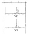
The example of the passband of Figure 12 A graphic extension wideband photodetector.
The example of the curve of spectrum of Figure 12 B graphic extension red LED.
The passband of Figure 12 C graphic extension wideband photodetector and the curve of spectrum of red LED both.
The example of the passband of the curve of spectrum of red LED of illumination degradation and wideband photodetector has been experienced in Figure 12 D graphic extension.
Figure 13 graphic extension is used for the embodiment of the process of calibration pixel element.
The example of the passband of Figure 14 A graphic extension red sensitive photoelectric detector.
The passband of Figure 14 B graphic extension red sensitive photoelectric detector and the curve of spectrum of red LED both.
The example of the passband of the curve of spectrum of red LED of illumination degradation and red sensitive photoelectric detector has been experienced in Figure 14 C graphic extension.
The example of the hue coordinate displacement of Figure 14 D graphic extension red LED and the passband of red sensitive photoelectric detector.
The example of the curve of spectrum of the red LED that Figure 14 E graphic extension is just being overdrived and the passband of red sensitive photoelectric detector.
The embodiment of the oar shape part of Figure 15 graphic extension composite display.
The embodiment of the oar shape part of Figure 16 graphic extension composite display.
Figure 17 graphic extension is used to calibrate the embodiment of process of the LED of oar shape part.
The passband of Figure 18 A graphic extension photoelectric detector.
The passband of two photoelectric detectors of Figure 18 B graphic extension.
Embodiment
The present invention can numerous modes implement, and comprises as process, equipment, system, composition of matter, computer-readable media (for example computer-readable storage medium) or wherein via the computer network of optics or the instruction of communication linkage router.In this manual, arbitrary other form that can take of these embodiments or the present invention can be called technology.The assembly (for example processor or memory) that is described as being configured to execute the task comprise temporarily be configured to preset time carry out described task general purpose module or through make with the specific components of carrying out described task both.In general, the order of the step of the process that discloses can be changed within the scope of the invention.
Hereinafter provide the detailed description of one or more embodiment of the present invention accompanying drawing together with the graphic extension principle of the invention.The present invention describes in conjunction with this type of embodiment, but the present invention is not limited to arbitrary embodiment.Scope of the present invention only contains numerous replacement schemes, modification and equivalents by claims restriction and the present invention.Set forth numerous specific detail to provide in describing in detail hereinafter to thorough of the present invention.These details are to provide for the example purpose, and can put into practice the present invention according to claims under the situation of the some or all of details in not having these specific detail.For the purpose of clear, do not describe technologic material known in the technical field related to the present invention as yet in detail in order to avoid unnecessarily obscure the present invention.
Fig. 1 is the diagram of the embodiment of the composite display 100 of graphic extension with single oar shape part.In the example of being showed, oar shape part 102 is configured to rotate with given frequency (for example 60Hz) around rotating shaft 104 at one end.Oar shape part 102 is in a rotation or oar shape part cycle period inswept regional 108.A plurality of pixel elements (for example LED) are installed on the oar shape part 102.As used herein, pixel element refers to any element of at least a portion that can be used for displays image information.As used herein, image or image information can comprise image, video, animation, lantern slide or displayable any other visual information.Other example of pixel element comprises: laser diode, phosphor, cathode ray tube, liquid crystal, any transmittance or emissivity optical modulator.Though can describe LED in the example in this article, can use any other suitable pixel element.In various embodiments, LED can disposed in various ways on oar shape part 102, as hereinafter more fully describing.
Oar shape part 102 inswept regional 108 o'clock, activate one or more among its LED between in due course, make beholder's perception one image or its part of watching scanning area 108.Image is made of the some pixels that have the locus separately.Can determine which locus specific LED is at any given point in time.When oar shape part 102 rotation, when overlapping, the locus of the pixel that each LED can be in its position and image activates according to circumstances.If oar shape part 102 spins just fast enough, so eyes perception consecutive image.This is because eyes have bad frequency response to illumination and color information.The integrated color that it is seen in window sometime of eyes.If with rapid serial several images that flash, eyes are integrated into single consecutive image with it so.The low time-sensitive degree of this of eyes is called the persistence of vision.
So, each LED on the oar shape part 102 can be used for a plurality of pixels in the display image.With at least one " the time pixel " in the viewing area of the single pixel mapping in the image in the composite display 100.The time pixel can be defined by pixel element on the oar shape part 102 and time (or position, angle of oar shape part), as hereinafter more fully describing.
The viewing area that is used for exploded view picture or video can have arbitrary shape.For instance, maximum viewing area is circular and identical with scanning area 108.Rectangular image or video can be shown in the rectangular display area 110, as demonstrated in scanning area 108.
Fig. 2 A is the diagram of the embodiment of the graphic extension oar shape part that is used for composite display.For instance, oar shape part 202,302 or 312 (discussing after a while) can be similar to oar shape part 102.Oar shape part 202 is shown as and comprises a plurality of LED206 to 216 and a rotating shaft 204, and oar shape part 202 is around described rotating shaft rotation.In various embodiments, LED206 to 216 can arbitrary suitable mode arrange.In this example, LED 206 to 216 makes it be evenly spaced apart each other and aims at along the length of oar shape part 202 through layout.Make LED 216 be adjacent to rotating shaft 204 on its edge in alignment with oar shape part 202.This makes that there is not blank spot in middle (around rotating shaft 204) when 202 rotations of oar shape part.In certain embodiments, oar shape part 202 is shape PCB as oar.In certain embodiments, oar shape part 202 other material shell of having aluminium, metal or being used to strengthen.
The example of the time pixel in Fig. 2 B graphic extension plane of scanning motion.In this example, each LED on the oar shape part 222 be associated around the anchor ring of rotating shaft (two circle between zone).Can whenever fan-shaped (angular spacing) activate once each LED.Activation LED can comprise the described LED of (for instance) connection and reach cycle stipulated time (for example, being associated with duty cycle) or turn-off described LED.Concentric circles and fan-shaped common factor form the zone corresponding to the time pixel.In this example, each time pixel has the angles of 42.5 degree, make to exist altogether 16 fan-shaped, can connect LED with the indication pixel described during fan-shaped.Owing to have 6 LED, therefore have 6*16=96 time pixel.In another example, the time pixel can have the angle of 1/10 degree, makes to have position, 3600 possibility angles altogether.
Because is uniformly at LED described in the given example along the spacing of oar shape part, so the time pixel becomes more intensive towards the center of display (near rotating shaft).Because image pixel is based on rectangular coordinate system definition, if therefore with image overlay on display, an image pixel can be corresponding to a plurality of time pixels that are close to display center so.On the contrary, in the most external office of display, an image pixel can be corresponding to the sub-fraction of a time pixel or a time pixel.For instance, two or more image pixels can be in single time pixel coverage.In certain embodiments, display makes that through design (for example, by changing the number/layout of the LED on fan-shaped time or the oar shape part) in the most external office of described display, there is at least one time pixel in every image pixel.This is in order to keep the level of resolution identical with image in display.In certain embodiments, how soon fan-shaped size by can the LED control data transmission being limited to activate LED to led driver.In certain embodiments, use the layout of LED on oar shape part to make the density of time pixel leap display more even.For instance, can be on oar shape part LED be placed to its more away from rotating shaft just the closer to together.
Fig. 3 is the diagram of the embodiment of the composite display 300 of graphic extension with two oar shape parts.In the example of being showed, oar shape part 302 is configured to rotate with given frequency (for example 60Hz) around rotating shaft 304 at one end.Oar shape part 302 is in a rotation or oar shape part cycle period inswept regional 308.A plurality of pixel elements (for example LED) are installed on the oar shape part 302.Oar shape part 312 is configured to rotate with given frequency (for example 60Hz) around rotating shaft 314 at one end.Oar shape part 312 is in a rotation or oar shape part cycle period inswept regional 316.A plurality of pixel elements (for example LED) are installed on the oar shape part 312. Scanning area 308 and 316 has lap 318.
For making big display, can in composite display, use an above oar shape part.For each oar shape part, can determine which locus specific LED is at any given point in time, the mode that therefore can be similar to the mode of describing with respect to Fig. 1 is represented arbitrary image by many oars shape part display.In certain embodiments, for lap 318, the LED that whenever cycles through will be many for the twice in the non-overlapped part.This can make the lap of display have higher illuminance at eyes.Therefore, in certain embodiments, when LED is in the lap, can activates it and reach half the time and make whole viewing area appear to be to have equal illumination.This example and other example of disposing the overlapping region hereinafter more fully described.
The viewing area that is used for exploded view picture or video can have arbitrary shape.Scanning area 308 and 316 union are maximum viewing area.Rectangular image or video can be shown in the rectangular display area 310, as demonstrated.
When using an above oar shape part, exist and guarantee the not variety of way of collision each other of contiguous oar shape part.The example of the oar shape part installing in Fig. 4 A graphic extension composite display.In these examples, show the cross section that is installed on the contiguous oar shape part on the axle.
In diagram 402, two contiguous oar shape parts rotate in the plane of scanning motion of vertical separation, thereby guarantee that described oar shape part will not collide when rotated.This mean described two oar shape parts can friction speed rotation and do not need homophase each other.Seem, if exploration on display resolution ratio fully less than the vertical interval between the different scanning plane, makes two oar shape parts rotate in the described plane of scanning motion so be to detect less than.In this example, described axle is in the center of described oar shape part.This embodiment is hereinafter more fully described.
In diagram 404, two oar shape parts rotate in the same scan plane.In the case, the rotation of described oar shape part is coordinated to avoid collision.For instance, described oar shape part rotation in phase each other.Other example of this situation is hereinafter more fully described.
Have under the situation on different scanning plane at two oar shape parts, when from the some viewing display area 310 at the center that is not orthogonal to viewing area 310, light can leak along diagonal between the plane of scanning motion.For instance, if pixel element emission unfocused light makes light launch with an angular range, this situation can take place so.In certain embodiments, use mask blocks from the light of a plane of scanning motion in order to avoid in another plane of scanning motion, see.For instance, mask is positioned over oar shape part 302 and/or oar shape part 312 back.Described mask can be attached to oar shape part 302 and/or 312 or with respect to oar shape part 302 and/or oar shape part 312 for fixing.In certain embodiments, (for example) for sheltering purpose, oar shape part 302 and/or oar shape part 312 are configured as and are different from the shape of being showed among Fig. 3 and the 4A.For instance, oar shape part 302 and/or oar shape part 312 can be through being shaped to shelter the scanning area of another oar shape part.
Fig. 4 B is the diagram of the embodiment of the graphic extension composite display 410 that uses mask.In the example of being showed, oar shape part 426 is configured to rotate with given frequency (for example 60Hz) around rotating shaft 414 at one end.A plurality of pixel elements (for example LED) are installed on the oar shape part 426.Oar shape part 426 is in a rotation or oar shape part inswept regional 416 (bold-faced dotted lines) of cycle period.Oar shape part 428 is configured to rotate with given frequency (for example 60Hz) around rotating shaft 420 at one end.Oar shape part 428 is in a rotation or oar shape part inswept regional 422 (bold-faced dotted lines) of cycle period.A plurality of pixel elements (for example LED) are installed on the oar shape part 428.
In this example, use mask 412 (solid line) in oar shape part 426 back.In the case, mask 412 is and regional 416 identical shapes (that is circle).Mask 412 is sheltered from the light of the pixel element on the oar shape part 428 in order to avoid leak in the scanning area 416.Mask 412 can be installed in oar shape part 426 back.In certain embodiments, mask 412 is attached to oar shape part 426 and spins around rotating shaft 414 with oar shape part 426.In certain embodiments, mask 412 be installed in oar shape part 426 back and with respect to oar shape part 426 for fixing.In this example, mask 418 (solid line) is installed in oar shape part 428 back in a similar manner.
In various embodiments, mask 412 and/or mask 418 can be made and had various colors by various materials.For instance, mask 412 and 418 can be black and is made of plastics.
The viewing area that is used for exploded view picture or video can have arbitrary shape.Scanning area 416 and 422 union are maximum viewing area.Rectangular image or video can be shown in the rectangular display area 424, as demonstrated.
Zone 416 and 422 is overlapping.As used herein, if two elements (for example, scanning area, the plane of scanning motion, mask, pixel element) intersect in the x-y projection, it is overlapping so.In other words, if described zone is projected on the x-y plane (defined by x axle and y axle, wherein x axle and y axle are in the plane of described figure), it intersects each other so.Same level (do not have identical z value, wherein the z axle is perpendicular to x axle and y axle) is not scanned in zone 416 and 422, but it overlaps each other in lap 429.In this example, mask 412 covers scanning area 422 at lap 429 or through shaded areas 429 places.It is because it is overlapped in scanning area 429 and is positioned on the top of scanning area 429 that mask 412 covers scanning area 429.
Fig. 4 C is the diagram of the embodiment of the graphic extension composite display 430 that uses mask.In this example, pixel element is attached to both rotating circular disks of structure as mask and described pixel element.Disk 432 can be considered the oar shape part of toroidal.In the example of being showed, disk 432 (solid line) is configured to rotate with given frequency (for example 60Hz) around rotating shaft 434 at one end.A plurality of pixel elements (for example LED) are installed on the disk 432.Disk 432 is in a rotation or disk inswept regional 436 (bold-faced dotted lines) of cycle period.Disk 438 (solid line) is configured to rotate with given frequency (for example 60Hz) around rotating shaft 440 at one end.Disk 438 is in a rotation or disk inswept regional 442 (bold-faced dotted lines) of cycle period.A plurality of pixel elements (for example LED) are installed on the disk 438.
In this example, described pixel element can be installed on disk 432 and 438 Anywhere.In certain embodiments, pixel element is installed on disk 432 and 438 with identical patterns.In other embodiments, on each disk, use different pattern.In certain embodiments, the density of pixel element is towards the center of each disk and lower, so the density of time pixel is being more even under the identical situation on the whole disk than the density at pixel element.In certain embodiments, pixel element is through placing so that time pixel redundancy (that is, placing an above pixel at the same radius place) to be provided.Every pixel has more pixel element and means and can reduce rotary speed.In certain embodiments, pixel element is through placing so that higher time pixel resolution to be provided.
The viewing area that is used for exploded view picture or video can have arbitrary shape.Scanning area 436 and 442 union are maximum viewing area.Rectangular image or video can be shown in the rectangular display area 444, as demonstrated.
In certain embodiments, pixel element is configured to not be activated covering at that time.For instance, being installed in pixel element on the disk 438 is configured to not be activated covering its (for example, with overlapping through shaded areas 439) time.In certain embodiments, described pixel element is configured to be not activated in the part of shaded areas.For instance, be configured to not be activated apart from the zone in a certain distance in the edge of shaded areas 439.This is positioned at the left side at center, viewing area or the right and can sees to can be under the situation of the marginal portion of shaded areas the beholder needs.
Fig. 5 is the block diagram of the embodiment of the graphic extension system that is used for display image.In the example of being showed, oar shape part panel 502 is the structure that comprises one or more oar shape parts.As hereinafter more fully describing, oar shape part panel 502 can comprise a plurality of oar shape parts, and it can comprise: the oar shape part of all size, length and width; Oar shape part around mid point or end points rotation; In the same scan plane or the oar shape part that in the different scanning plane, rotates; Each other homophase or not in phase the rotation oar shape part; Oar shape part with a plurality of arms; And oar shape part with other shape.Oar shape part panel 502 can comprise all identical oar shape part or various oar shape parts.Described oar shape part can be arranged to grid or arbitrary other layout.In certain embodiments, described panel comprises angle detector 506, and it is used for detecting the one or more angles that are associated with described oar shape part.In certain embodiments, there is the angle detector that is used for each oar shape part on the oar shape part panel 502.For instance, can fluorescence detector be installed to detect its current angle near oar shape part.
In certain embodiments, use look-up table to implement pixel map 508, as hereinafter more fully describing.At different images, use different look-up tables.Pixel map 508 is hereinafter more fully described.
In certain embodiments, do not need use angle detector 506 to come reading angular.Because it is predetermined that the angular speed of described oar shape part and the initial angle (under described angular speed) of described oar shape part can be, therefore which kind of angle can calculate oar shape part is at any given point in time.In other words, can determine described angle based on the time.For instance, if described angular speed is ω, the position, angle after time t is θ so
Initial+ ω t, wherein θ
InitialFor in case oar shape part will be with the initial angle of stable state from supination.So, the LED control module can be exported the LED control data continuously according to time (for example, using clock), but not uses from the angular surveying of angle detector 506 outputs.For instance, but settling time table (for example, clock circulation) to the LED control data.
In certain embodiments, when oar shape part will be from static startup, its experience initiating sequence and ramp up to stable state angular speed.In case it reaches described angular speed, the initial angle of just measuring described oar shape part is in which kind of angle (and determining which point place in LED control data sequence starts) to calculate a described oar shape part time point in office.
In certain embodiments, optionally and periodically use angle detector 506 provides adjustment.For instance, if described angle is drifted about, can make the displacement of LED control data output tape sorting so.In certain embodiments, if angular speed drifts about, carry out mechanical adjustment so to adjust described speed.
Fig. 6 A is the diagram of the embodiment of the composite display 600 of graphic extension with two oar shape parts.In the example of being showed, indicate polar coordinate system on each in zone 608 and 616, wherein initial point is positioned at each rotating shaft 604 and 614 places.In some embodiments, write down the position of each LED on oar shape part 602 and 612 with polar coordinates.Distance from the initial point to LED is a radius r.Oar shape part angle is θ.For instance, if oar shape part 602 at 3 o ' clock positions, so each among the LED on the oar shape part 602 be 0 the degree.If oar shape part 602 is at 12 o'clock, each among the LED on the oar shape part 602 is 90 degree so.In certain embodiments, the use angle detector detects the current angle of each oar shape part.In certain embodiments, the time pixel is by P, r and θ definition, and wherein P is an oar shape part identifier and (r θ) is the polar coordinates of LED.
On image to be shown 610, indicate rectangular coordinate system.In this example, initial point is positioned at the center of image 610, but it can be positioned at Anywhere, and this decides on embodiment.In certain embodiments, by each pixel mapping in the image 610 is created pixel map 508 to one or more time pixels in viewing area 608 and 616.In various embodiments, can carry out mapping in every way.
Fig. 6 B is the flow chart of the embodiment of the graphic extension process that is used to produce pixel map.For instance, can use this process to create pixel map 508.At 622 places, obtain image pixel to the time pixel mapping.In certain embodiments, by (rectangular pixels of wherein said image (x, y) grid is corresponding to the resolution of described image) is superimposed on zone 608 and 616, and (described zone has two utmost point time pixel (r, θ) grids with image 610, for example, referring to Fig. 2 B) on carry out mapping.(x y), determines which time pixel is in described image pixel at each image pixel.Below be the example of pixel map:
| Image pixel (x, y) | The time pixel (P, r, θ) | Intensity (f) |
| (a1,a2) | (b1,b2,b3) | |
| (a3,a4) | (b4,b5,b6);(b7,b8,b9) | |
| (a5,a6) | (b10,b11,b12) | |
| Or the like | Or the like |
Table 1
As discussed previously, an image pixel can be mapped to a plurality of time pixels, and is indicated as second row.In certain embodiments, use index to substitute r corresponding to LED.In certain embodiments, at various image sizes and resolution (for example, normally used image size and resolution) in advance the computed image pixel to the time pixel mapping.
At 624 places, fill intensity f at each image pixel based on image to be shown.In certain embodiments, the f indication LED should be connected (for example, 1) and still should turn-off (for example, 0).For instance, in black and white image (not having the gray scale rank), black picture element is mapped to f=1 and white pixel is mapped to f=0.In certain embodiments, f can have fractional value.In certain embodiments, use duty cycle to manage and implement f.For instance, when f is 0, in the described fan-shaped time, do not activate described LED.When f is 1, activates described LED and reach the described whole fan-shaped time.When f is 0.5, activate half that described LED reaches the described fan-shaped time.In certain embodiments, f can be used for display gray scale rank image.For instance, if there are 256 gray scales in the image, the pixel that has gray scale 128 (half illumination) so will have f=0.5.In certain embodiments, be not to use duty cycle (that is, pulse width modulation) to implement f, but implement f by the electric current (that is pulse-height modulation) of adjusting to LED.
For instance, after filling intensity f, described table can be revealed as follows:
| Image pixel (x, y) | The time pixel (P, r, θ) | Intensity (f) |
| (a1,a2) | (b1,b2,b3) | ?f1 |
| (a3,a4) | (b4,b5,b6);(b7,b8,b9) | ?f2 |
| (a5,a6) | (b10,b11,b12) | ?f3 |
| Or the like | Or the like | Or the like |
Table 2
At 626 places, carry out optional pixel map and handle.This can comprise to the overlapping region compensate, make the center illumination (that is the time pixel that, wherein has higher density) balance, make use balance of LED or the like.For instance, when LED is arranged in overlapping region (and/or on border of overlapping region), can reduce its duty cycle.For instance, in composite display 300, when LED is arranged in overlapping region 318, its duty cycle is reduced by half.In certain embodiments, in the fan-shaped time, there are a plurality of LED, in the case, can activate and be less than all LED (that is can be 0 with a few thing cycle sets in the duty cycle) corresponding to the single image pixel.In certain embodiments, described LED can be activated (for example, every N circulation, wherein N is an integer) in turn, for example so that use balance, makes a LED can earlier not burn out than other LED.In certain embodiments, described LED is the closer in the center (the time pixel that wherein has higher density), and its duty cycle is just low more.
For instance, after candle balance, pixel map can be revealed as follows:
| Image pixel (x, y) | The time pixel (P, r, θ) | Intensity (f) |
| (a1,a2) | (b1,b2,b3) | ?f1 |
| (a3,a4) | (b4,b5,b6) | ?f2 |
| (a5,a6) | (b10,b11,b12) | ?f3 |
| Or the like | Or the like | Or the like |
Table 3
As demonstrated, in second row, deleted the second time pixel so that cross over the candle balance of pixel.This also may realize to f2/2 by intensity is reduced by half.As another replacement scheme, can the circulation between alternately turn-on time pixel (b4, b5, b6) and (b7, b8, b9).In certain embodiments, this can be instructed in the described pixel map.In different embodiments, can use various data structures to implement described pixel map in every way.
For instance, in Fig. 5, the time Pixel Information (P, r, θ and f) that LED control module 504 is used from described pixel map.LED control module 504 is got θ as input and output LED control data P, r and f.The described LED control data of oar shape part panel 502 uses activates LED and reaches the described fan-shaped time.In certain embodiments, have the led driver that is used for each oar shape part, it uses described LED control data to determine to connect (if any) which LED in each fan-shaped time.
Any image (comprising video) data can be input to LED control module 504.In various embodiments, can live ground or (that is, just before display image) calculating 622,624 and 626 in real time in one or more.This can be used for the live broadcast of image, for example the live video of stadium.For instance, in certain embodiments, calculate 622 and live ground or calculate 624 in real time in advance.In some embodiments, can before 622, carry out 626 by suitably revising described pixel map.In certain embodiments, 622,624 and 626 all is precalculated.For instance, because advertising image normally knows in advance, therefore can calculate described advertising image in advance.
In various embodiments, the process of execution graph 6B in every way.It is as follows how to carry out another example of 622.(x y), calculates polar coordinates at each image pixel.For instance, image pixel (center) is converted to the polar coordinates (if can there be a plurality of polar coordinates set so in described image pixel and overlapping scan region overlapping) of its overlapping with it scanning area.The polar coordinates that calculated are rounded to nearest time pixel.For instance, select its center to be close to polar time pixel of being calculated most.If (have a plurality of polar coordinates set, select its center to be close to polar time pixel of being calculated most so.) in this way, each image pixel is mapped to time pixel at the most.This can be desirable, because it keeps the uniform density (that is, the density through the activationary time pixel near rotating shaft is not higher than edge) through the activationary time pixel in the viewing area.For instance, the pixel map of being showed in the substitution tables 1 can obtain following pixel map:
| Image pixel (x, y) | The time pixel (P, r, θ) | Intensity (f) |
| (a1,a2) | (b1,b2,b3) | |
| (a3,a4) | (b7,b8,b9) | |
| (a5,a6) | (b10,b11,b12) | |
| Or the like | Or the like |
Table 4
In some cases, use this technology that rounds off, two image pixels can be mapped to identical time pixel.In the case, can use various technology at 626 places, including (for example): the intensity of two rectangular pixels is asked average and assigned described mean value for a time pixel; Between circulation, between first and second rectangular pixels intensity, replace; Replays in the image pixel are mapped to nearest neighbor time pixel; Or the like.
Fig. 7 graphic extension is arranged to the example of the oar shape part of various arrays.For instance, any one comprised oar shape part panel 502 in these arrays.Arbitrary number oar shape part can be combined into an array to form the viewing area of any size and shape.
Arrange that 702 show eight circular scan zones corresponding to eight oar shape parts that have identical size separately.Described scanning area is overlapping like that as demonstrated.In addition, show rectangular display area on each scanning area.For instance, the maximum rectangular display area of this layout will comprise the union of all rectangular display area of being showed.For fear of have the gap in maximum viewing area, the maximum spacing between the rotating shaft is
 R, wherein R is the radius in one in the described circular scan zone.Spacing between the axle makes that the periphery of a scanning area is not overlapping with any rotating shaft, otherwise will have interference.Can use arbitrary combination of described scanning area and rectangular display area to show one or more images.
In certain embodiments, described eight oar shape parts are in the same scan plane.In certain embodiments, described eight oar shape parts are in the different scanning plane.Can minimize employed plane of scanning motion number.For instance, might make every an oar shape part scanning same scan plane.For instance, scanning area 710,714,722 and 726 can be in the same scan plane, and scanning area 712,716,720 and 724 can be in another plane of scanning motion.
In some configurations, scanning area (for example, scanning area 710 and 722) overlaps each other.In some configurations, scanning area (for example, scanning area 710 makes it only contact at a some place with 722 removable separating) tangent to each other.In some configurations, scanning area does not overlap each other (for example, scanning area 710 and 722 has little gap between it), this display the resolution of wanting be acceptable under for fully low situation.
Arrange that 704 show ten circular scan zones corresponding to ten oar shape parts.Described scanning area is overlapping like that as demonstrated.In addition, show rectangular display area on each scanning area.For instance, can use three rectangular display area (in each scanning area row one) to come (for example) to show three independent advertising images.Can use arbitrary combination of described scanning area and rectangular display area to show one or more images.
Arrange that 706 show seven circular scan zones corresponding to seven oar shape parts.Described scanning area is overlapping like that as demonstrated.In addition, show rectangular display area on each scanning area.In this example, described oar shape part has all size and makes described scanning area have different sizes.Can use arbitrary combination of described scanning area and rectangular display area to show one or more images.For instance, can use all scanning areas as a viewing area that is used for non-rectangular shape image (for example segment of huge snake).
Fig. 8 graphic extension has the example of coordinated simultaneous movements with the oar shape part that prevents mechanical disturbance.In this example, the array of showing eight oar shape parts at three time points.Described eight oar shape parts are configured in phase move each other; That is to say that at each time point, each oar shape part is along equidirectional orientation (maybe being associated with equal angular when the polar coordinate system described in using Fig. 6 A).
Fig. 9 graphic extension has the example of coordinated out-of-phase motion with the oar shape part that prevents mechanical disturbance.In this example, the array of showing four oar shape parts at three time points.Described four oar shape parts are configured to out of phase move each other; That is to say that at each time point, at least one oar shape part is not along the direction orientation identical with other oar shape part (maybe being associated with the angle identical with other oar shape part when the polar coordinate system described in use Fig. 6 A).In the case, instant described oar shape part out of phase moves each other, and its phase difference (differential seat angle) also makes its not mechanical disturbance each other.
Display system described herein has the built-in cooling system of nature.Because described oar shape part spins, therefore discharge heat from described oar shape part naturally.LED is far away more apart from rotating shaft, and the cooling of its reception is just many more.In certain embodiments, at least 10 times of ground of the cooling of this type are effective in the wherein system of LED tile for fixing and wherein use the external refrigeration system to blow air with the use fan above described LED tile.In addition, because of not using the external refrigeration system to realize remarkable cost savings.
Though in the example in this article, image to be shown provides with the pixel that is associated with rectangular coordinate and the viewing area is associated with the time pixel of describing with polar coordinates, technology herein can be used from image or viewing area with arbitrary coordinate system one.
Move though describe the rotation of oar shape part herein, also can use the moving of any other type of oar shape part.For instance, move about oar shape part can be configured to (thereby produce the rectangular scanning zone, suppose that LED aims at along straight row).Oar shape part can be configured to rotation and move (thereby producing oval scanning area) about the while.Oar shape part can have and is configured and extends and the arm of withdrawal with some angles, for example to produce bigger rectangular scanning zone.Because therefore known described moving can be determined pixel map, and can use technology described herein.
Figure 10 is the diagram of example of the cross section of the oar shape part in the graphic extension composite display.This examples show is for comprising oar shape part 1002, axle 1004, optical fiber 1006, optical camera 1012 and optical data transmission device 1010.Oar shape part 1002 is attached to axle 1004.Axle 1004 passes its center through bore hole (that is hollow) and optical fiber 1006 continuities.The pedestal 1008 of optical fiber 1006 receives data via optical data transmission device 1010.Described data are along upwards transmission and be transferred to fluorescence detector (showing) on the oar shape part 1002 at 1016 places of optical fiber 1006.Described fluorescence detector is provided to described data one or more led drivers that are used to activate one or more LED on the oar shape part 1002.In certain embodiments, the LED control data transmission that will receive from LED control module 504 in this way is to led driver.
In certain embodiments, axle 1004 pedestal has by optical camera 1012 and reads to determine the suitable mark 1014 when the anterior angle position of oar shape part 1002.In certain embodiments, optical camera 1012 is used in combination with output with angle detector 506 and is fed to the angle information of LED control module 508 as show in Figure 5.
It is can be along with it aging and demote to constitute the performance of the pixel element of composite display.The degradation of pixel element is tangible at two kinds in form: the reduction in time of the intensity of pixel element or illumination and/or the curve of spectrum hue coordinate displacement in time of pixel element.In some cases, it is the degradation first-order effects that illumination reduces (that is, it is darker that pixel element becomes), and the spectral shift of pixel element is a second-order effects.As hereinafter further describing, the oar shape part of composite display can comprise the degradation that helps to detect pixel element makes that the pixel element of described composite display can be through periodically calibrating to proofread and correct and/or to improve one or more assemblies of performance degradation at least in part.
In certain embodiments, one or more optical pickocffs (for example, photoelectric detector, photodiode etc.) are installed on each oar shape part of composite display and are used for measuring the light intensity or the illumination of being launched by the pixel element on the described oar shape part.Though can describe photoelectric detector in the example in this article, can adopt any suitable optical pickocff.The type that is installed in the photoelectric detector on the oar shape part depends on the type of the pixel element degradation that needs detect and proofread and correct.For instance, only need therein to detect under the situation of pixel element degradation first-order effects (that is, illumination reduces), wideband photodetector can be sufficient.Yet,, can need red sensitive, green sensitive and/or blue sensitive photo-detectors in addition so if also need to detect the hue coordinate displacement.As hereinafter further describing; in various embodiments; the part that can make the light that pixel element launches is reflected back and is received by corresponding photoelectric detector by the structure of the front surface that is used to protect composite display, and the part that perhaps can make the light that pixel element launches is by the direction focusing of the customization lenslet that is attached to described pixel element along corresponding photoelectric detector.Be installed in photoelectric detector on the oar shape part baseline brightness value when can be used to measure during making or being provided with calibration pixel element at first.In certain embodiments, when determining the baseline brightness value of pixel element, turn-off other pixel element (for example, near pixel element or all pixel elements on the oar shape part).During the subsequent calibrations at the scene, photoelectric detector can be used to measure the current brightness value of pixel element.The current brightness value of pixel element can be compared with the baseline brightness value of measuring when the initial calibration pixel element that is associated.Suitably adjust the electric current of driving pixel element at the scene between alignment epoch under the situation of having demoted its brightness value is returned to its baseline value at described pixel element.Also can adopt the current brightness value of pixel element to detect the color displacement.For instance, by make one or more pixel elements that are associated with not enough color overdrive and make one or more pixel elements that are associated with excessive color owe to drive so that described color again balance proofread and correct the color displacement.
The embodiment of the oar shape part of Figure 11 A graphic extension composite display.Oar shape part 1100 comprises around the PCB disk of rotating shaft 1102 rotations.Pixel element radially is installed on the oar shape part 1100 and in given example and is described by little square.Photoelectric detector also is installed on the oar shape part 1100 and in given example and is described by small circular.In various embodiments, each photoelectric detector can be associated with intensity or the illumination of measuring arbitrary number pixel element.For instance, in certain embodiments, be installed on the oar shape part each photoelectric detector with 5 to 10 radially the set of neighborhood pixels element be associated.In the example of Figure 11 A, each photoelectric detector with five radially the set of neighborhood pixels element be associated.For instance, photoelectric detector 1104 is associated with each illumination in measuring pixel element 1106.Make the part of the light that each pixel element of set in 1106 launch reflect back and/or otherwise receive by photoelectric detector 1104 towards photoelectric detector 1104.By the intensity of each pixel element or distance and/or the angle that illumination depends on described pixel element and photoelectric detector 1104 at least in part in the set 1106 of photoelectric detector 1104 measurements, wherein measure lower intensity at the pixel element that is positioned at a distance.Therefore, when calibrating the pixel element of oar shape part 1100 during manufacture, can be at set each pixel element in 1106 by the photoelectric detector 1104 that is associated based on distance and/or the angular surveying different baseline brightness values of described pixel element with described photoelectric detector.Only need therein to detect under the situation that also illumination of correction pixels element reduces, described photoelectric detector can comprise wideband photodetector.For instance, pixel element comprises under the situation of White LED therein, and the degradation of LED can at least mainly cause the illumination of described LED to reduce.Under this type of situation, can adopt wideband photodetector periodically to measure the brightness value of described LED, if and found that LED has the illumination lower than its baseline value, the electric current that can suitably have additional supply of described LED would so turn back to its baseline value with the illumination with described LED.In certain embodiments, the pixel element of oar shape part 1100 can comprise color LED, that is, and and redness, green and/or blue led.Figure 11 B graphic extension wherein each pixel element array of oar shape part 1100 comprises the embodiment of redness (R), green (G) or blue (B) LED.Under this type of situation, reduce if only need to detect and proofread and correct illumination, so also can adopt wideband photodetector.
The example of the passband of Figure 12 A graphic extension wideband photodetector, ideally, described photoelectric detector is to the same sensitivity of illumination (that is, can detect the illumination of all optical wavelength) from all optical wavelength.The example of the curve of spectrum of Figure 12 B graphic extension red LED.As depicted, described curve is the center with the wavelength of 635nm.The curve of spectrum of the passband of the wideband photodetector of Figure 12 C graphic extension Figure 12 A and the red LED of Figure 12 B both.In certain embodiments, (that is the part of being caught by photoelectric detector of the curve of spectrum of described red LED) determines the illumination of described red LED from the shadow region of Figure 12 C.The example of the passband of the curve of spectrum of red LED of illumination degradation and wideband photodetector has been experienced in Figure 12 D graphic extension.As depicted, to catch the zone with respect to Figure 12 C be littler zone to the photoelectric detector among Figure 12 D.Can make illumination with described LED return to its baseline value to proofread and correct this illumination and reduce by increasing the electric current just driving described LED, for example, as describing among Figure 12 B and the 12C.
Figure 13 graphic extension is used for the embodiment of the process of calibration pixel element.In certain embodiments, employing process 1300 comes the illumination of correction pixels element to reduce, described illumination reduce can (for instance) by the aging generation of described pixel element.Process 1300 begins at 1302 places, determines the current brightness value of particular pixel element at 1302 places.For instance, can determine the current brightness value of described pixel element from the measured intensity level of the photoelectric detector that is associated with described pixel element.At 1304 places, (for example, making or be provided with during) determined and the baseline brightness value of the described pixel element stored compares during the current brightness value of the described pixel element that will determine at 1302 places and the initial calibration of the composite display that is being associated.At 1306 places, whether the current brightness value of determining described pixel element is with respect to its baseline value degradation.If the current brightness value of determining described pixel element at 1306 places is not as yet with respect to its baseline value degradation, so owing to do not need to proofread and correct calibration so process 1300 end that illumination reduces.If determine the current brightness value of described pixel element demotes (promptly with respect to its baseline value at 1306 places, described current brightness value is than its baseline value little (for example) ormal weight), the electric current that increases the described pixel element of driving so is so that the current brightness value of described pixel element goes back up to its baseline value, and process 1300 finishes subsequently.In certain embodiments, process 1300 is used for each of at least one pixel element subclass of composite display between alignment epoch.
Such as description, illumination reduces a kind of effect that (that is, pixel element becomes darker) can be performance degradation.In some cases, hue coordinate displacement can be (comprising the displacement by the peak wavelength of pixel element emission) another effect of performance degradation.If only need to detect and the illumination or the brightness of correction pixels element reduces, so as the description wideband photodetector can be abundance.In certain embodiments, need to detect the colourity change of described pixel element.For instance, if composite display comprises color LED, may (for instance) the hue coordinate displacement take place along with the aging of described LED so.
In certain embodiments, composite display comprises the colour element element, for example redness, green and blue led.Under this type of situation, can adopt red sensitive, green sensitive and blue sensitive photo-detectors to help detect the color displacement of corresponding color LED.For instance, can adopt the red sensitive photoelectric detector to measure the intensity or the illumination of red LED.For detecting red light and filtering other color, the passband of red sensitive photoelectric detector covers the wavelength that is associated with red LED.The example of the passband of Figure 14 A graphic extension red sensitive photoelectric detector.The curve of spectrum of the passband of the red sensitive photoelectric detector of Figure 14 B graphic extension Figure 14 A and the red LED of Figure 12 B both.In certain embodiments, (that is the part of being caught by described photoelectric detector of the curve of spectrum of described red LED) determines the illumination of described red LED from the shadow region of Figure 14 B.The example of the passband of the curve of spectrum of red LED of illumination degradation and red sensitive photoelectric detector has been experienced in Figure 14 C graphic extension.As depicted, to catch the zone with respect to Figure 14 B be littler zone to the photoelectric detector among Figure 14 C.Can use as mentioned and detect the illumination degradation that detects by the red sensitive photoelectric detector among Figure 14 C in a similar manner with respect to the described wideband photodetector of Figure 12 D.The example of the hue coordinate displacement of Figure 14 D graphic extension red LED and the passband of red sensitive photoelectric detector.As depicted, the peak wavelength of described red LED floats to 620nm (that is, towards green) from 635nm.Be similar among Figure 14 C, the zone that the red sensitive photoelectric detector among Figure 14 D is caught with respect to Figure 14 B is littler zone.Yet, only use wideband photodetector originally may detect hue coordinate displacement (because its all-pass is crossed due to the character) less than Figure 14 D, even therefore spectrum is shifted, also will capture the zone that is similar to the zone among Figure 12 C.
Suppose that the shadow region among Figure 14 C equates that with shadow region among Figure 14 D then described in both cases red sensitive photoelectric detector will detect the equal illumination value.Can with the brightness value that detects by described red sensitive photoelectric detector with during fabrication or the baseline value of during being provided with, determining compare, make that can discern illumination reduces.Than low-light (level) measuring by described red LED become in the situation of Figure 14 C given birth to than the abortion within the first month of pregnancy, and in the situation of Figure 14 D than low-light (level) measure by the peak wavelength displacement of described red LED and therefore described red sensitive photoelectric detector only catch described red LED spectrum tail end and produce.Can make that the illumination of described LED can be returned to its baseline value proofreaies and correct through identification illumination and reduce by the electric current that increases driving LED.Under the situation of Figure 14 C, increase the electric current that drives red LED and cause the illumination of described red LED is returned to its baseline value up to measuring the baseline brightness value, for example, as describing among Figure 14 B.Under the situation of Figure 14 D, the electric current that increase to drive described red LED is up to measuring the baseline brightness value described red LED (describing in as Figure 14 E) that causes overdriving considerablely, and this is because described red sensitive photoelectric detector is only just being caught the tail end (because its hue coordinate be shifted due to) of the spectrum of described red LED.
In certain embodiments, comprise red sensitive, green sensitive and blue sensitive photo-detectors in the colored composite display to help calibration redness respectively, green and blue led.Comprise at colored composite display under the situation of redness, green and blue led, overdrive one or more tone or colourities displacements that make white light among the described LED, this by activate simultaneously with reproduce described display in special time pixel (and/or time pixel set or ring) redness, green and the blue led generation that are associated.Under this type of situation, white can no longer be revealed as white.For instance, at the composite display that comprises the redness, green and the blue led that are used for each time pixel, if red LED is towards green drift and overdrived (for example describing among Figure 14 E) and blueness and green LED do not need to adjust and therefore do not adjusted, so white (it will reproduce by activating all three color LEDs) will have slight green color and luster.Therefore, under this type of situation, the displacement that can need to discern the hue coordinate displacement of specific color LED and/or discern the colourity of white.In red sensitive, green sensitive and the blue sensitive photo-detectors each only helps to determine that illumination (for example changes, reduce) and can't (for example change in the illumination that changes generation by brightness, the situation of Figure 14 C) illumination that produces with displacement by the peak wavelength of LED changes between (for example, the situation of Figure 14 D) and distinguishes.In certain embodiments, except indivedual color photoelectric detectors, also adopt broadband or white sensitive photo-detectors.One or more if overdrive in the color LED, so Bai Se illumination will than measure (for example, making or be provided with during) during the initial calibration of composite display and the baseline value of record much higher.Under this type of situation, can individually make progress and the electric current of the color LED during calibration process, adjusted of downward fine tuning, the illumination of measuring white is simultaneously just causing the increase of the illumination of white from its baseline value to discern which (which) color LED.
Can take one or more suitably to take action so that the colourity of white and/or the illumination of white are returned to its baseline value.In certain embodiments, not enough color is overdrived make simultaneously excessive color to owe to drive and return to its baseline value to remove in the white towards the colour cast of specific color or color and luster and/or with the illumination of white.For instance, red LED towards green drift describe in the example, can make green LED owe to drive so that the balance of overdriving of red LED.In certain embodiments, can be globally or redefine wavelength in time the change of chromaticity diagram to take into account primary colors of display partly.At first, when the image pixel with particular source image is mapped to the time during pixel, definition is with the color map of the described source images color map in the available color space of display.If during calibration process, find to have taken place one or more hue coordinate displacements, so in certain embodiments, the color map of whole display can be redefined and be the color space corresponding to the minimal gamut that can use for the time pixel in the described display.In some cases, this overall color remaps may be for unnecessary, and redefine color map partly at the time pixel of being reproduced by the LED that experiences the hue coordinate displacement and can be sufficient.This part remaps and can be sufficiently, changes because be difficult to the slight color of perception for eyes.For instance, for eyes, can be difficult to the difference of perception, especially very hour in the zone that is associated with each time pixel by the red LED of peak wavelength red time pixel of reproducing and the red time pixel of reproducing by the red LED of peak wavelength with 620nm with 635nm.
The embodiment of the oar shape part of Figure 15 graphic extension composite display.Oar shape part 1500 is configured to around rotating shaft 1502 rotation and inswept circular scan zones.For instance, oar shape part 1500 is similar to the oar shape part 302 and 312 and/or the oar shape part 426 and 428 of Fig. 4 B of oar shape part 222, Fig. 3 of oar shape part 102, Fig. 2 B of Fig. 1.Redness (R) alternately, green (G) and blue (B) LED install and are described by little square in given example along the length of oar shape part 1500.The time pixel ring that each redness, green and blue led in distance rotating shaft 1502 given radius capable (for example top line 1504) is associated with reproduction and described radius is associated.Red sensitive (R), green sensitive (G), blue responsive (B) and broadband or responsive (W) photoelectric detector of white also are installed on the oar shape part 1500 and in given example to be described by small circular.In the oar shape part configuration of Figure 15, with respect to the capable execution calibration of each LED.In various embodiments, each photoelectric detector can be associated with intensity or the illumination of measuring arbitrary number LED.In the example of Figure 15, each color sensitivity photoelectric detector is associated with the set of five LED of corresponding color, and each wideband photodetector and five LED line correlation connection.For instance, photoelectric detector set 1506 is associated with LED capable 1508.Each color sensitivity photoelectric detector is associated with the illumination of measuring corresponding color LED.For instance, the illumination of each red LED in the red sensitive photoelectric detector of set in 1506 and the measurement row 1508 is associated.The illumination of measuring white when broadband or white sensitive photo-detectors and (for example) are activated all three color LEDs of particular row at the same time is associated.For instance, measurement illumination is associated during all LED in the wideband photodetector of set in 1506 and the particular row (for example row 1504) in activating row 1508.Make the part of the light that each LED launches reflect back and/or otherwise receive by corresponding photoelectric detector towards corresponding photoelectric detector.The intensity of the intensity of the described LED that measures by corresponding color sensitivity photoelectric detector or brightness value and the white measured at described row by the white sensitive photo-detectors that is associated or distance and/or the angle that brightness value depends on described LED and described photoelectric detector at least in part.Therefore, during making or being provided with, during the LED of initial calibration oar shape part 1500, can measure different baseline brightness values and can measure different baselines white brightness values at each LED at each row.Described baseline value and the measured value of (for example, at the scene) during subsequent calibrations are compared.
The embodiment of the oar shape part of Figure 16 graphic extension composite display.Oar shape part 1600 comprises the PCB disk that is configured to around rotating shaft 1602 rotations.For instance, oar shape part 1600 is similar to the oar shape part 432 and 438 or the oar shape part 1100 of Figure 11 B of Fig. 4 C.Redness (R) alternately, green (G) and blue (B) led array are installed along the radius of oar shape part 1600, and in given example, described LED is described by little square.In certain embodiments, the LED in the center that is positioned at rotating shaft 1602 places of oar shape part 1600 comprises three look RGB LED.The time pixel ring that is associated with reproduction and described radius at the LED of distance rotating shaft 1602 specific radius (for example LED that intersect with ring 1604) is associated.In given example, each LED ring comprises two LED of each primary colors.Red sensitive (R), green sensitive (G), blue responsive (B) and broadband or responsive (W) photoelectric detector of white also are installed on the oar shape part 1600 and in given example to be described by small circular.In the oar shape part configuration of Figure 16, carry out calibration with respect to each LED ring (for example encircling 1604).In various embodiments, each photoelectric detector can be associated with intensity or the illumination of measuring arbitrary number LED.In the example of Figure 16, each color sensitivity photoelectric detector and corresponding color four or five the radially set of contiguous LED are associated, and each wideband photodetector is encircled with seven LED and is associated.In given example, the color sensitivity photoelectric detector is close to the led array of corresponding color and installs, and wideband photodetector is installed in the middle of the described led array.The illumination of measuring white when in certain embodiments, described wideband photodetector is with all LED of activating specific ring at the same time is associated.Can adopt a plurality of wideband photodetector that are associated with specific ring to determine the illumination of the white of described ring.In some cases, can adopt the mean value of the brightness value of measuring by a plurality of wideband photodetector to determine the illumination of a white of encircling.Because LED on the oar shape part (for example oar shape part 1600) and wideband photodetector configuration can make indivedual wideband photodetector illumination reading towards one or more color colour casts, therefore can ask average to this of a plurality of illumination reading.For instance, in the reading of each in the wideband photodetector of oar shape part 1600 redness-green, green-blueness or blueness-red colour cast can take place.Therefore, for the illumination of the white that obtains the ring in the oar shape part 1600, can be to asking average from the illumination number of degrees of two or more wideband photodetector that are associated with described ring.Make the part of the light that each LED launches reflect back and/or otherwise receive by corresponding photoelectric detector towards corresponding photoelectric detector.The intensity of the intensity of the described LED that measures by corresponding color sensitivity photoelectric detector or brightness value and the white measured at described ring by the white sensitive photo-detectors that is associated or distance and/or the angle that brightness value depends on described LED and described photoelectric detector at least in part.Therefore, during making or being provided with, during the LED of initial calibration oar shape part 1600, can measure different baseline brightness values and can measure different baselines white brightness values at each LED at each ring.Described baseline value and the measured value of (for example, at the scene) during subsequent calibrations are compared.
Figure 17 graphic extension is used to calibrate the embodiment of process of the LED of oar shape part.In certain embodiments, the brightness value that employing process 1700 is proofreaied and correct described LED reduces and/or the hue coordinate displacement, and for instance, described reduction and/or displacement can be by the aging generations of described LED.In certain embodiments, employing process 1700 calibrate with reproduce composite display in the LED that is associated of each time pixel ring.For instance, can adopt process 1700 to calibrate each LED capable (for example, the row among Figure 15 1504) or each LED ring (for example ring among Figure 16 1604).Process 1700 begins at 1702 places, will return to its baseline value with the illumination of reproducing each LED that special time pixel ring be associated at 1702 places, if necessary (that is, if its demote).In certain embodiments, recover the illumination of LED in the process 1300 of 1702 places employing Figure 13.The use color sensitivity photoelectric detector that is associated is determined the illumination of color LED.At 1704 places, all LED that activation and the described time pixel ring of reproduction are associated.At 1706 places, determine the current illumination of white at described ring.Use one or more broadbands or white sensitive photo-detectors to determine described white illumination.In some cases, can on average come to determine described white illumination by the illumination reading of two or more wideband photodetector is asked.At 1708 places, whether the current illumination of determining at 1706 places the white determined is than baseline brightness value height (for example) ormal weight of white.The baseline illumination of white is definite and storage (for example, during manufacturing or being provided with) during the initial calibration of the composite display that is associated.Be not higher than its baseline value (for example, ormal weight) if determine the current illumination of white at 1708 places, process 1700 finishes so.Under some these type of situations, can suppose not take place as yet the displacement of essence hue coordinate.Be higher than its baseline value (for example, ormal weight) if determine the current illumination of white at 1708 places, process 1700 proceeds to 1710 so.At 1710 places, individually modulation (for example, be delivered to the electric current of each LED that its illumination once was resumed at 1702 places upwards and downwards), measure the LED of current illumination to determine just to be overdrived and compensate of white simultaneously with to its hue coordinate displacement, that is, just causing the illumination of white to surpass the LED of its baseline value with identification.At 1712 places, take one or more suitably to take action and return to its baseline value, and process 1700 finishes subsequently with colourity and/or white illumination with white.For instance, can make another color LED owe to drive towards the color of its displacement so that described color balance.In some cases, can be globally or redefine the chromaticity diagram of (based on the available colour gamut of minimum) described display partly at the LED that is associated with described ring at whole display.
The process 1700 of Figure 17 is the example of collimation technique.In other embodiments, can adopt any other suitable collimation technique and/or technical combinations.For instance, adoptable another collimation technique comprises and uses wideband photodetector to measure the current brightness value of LED and described value and baseline broadband brightness value are compared, and uses corresponding color sensitivity photoelectric detector to measure the current brightness value of described LED and described value and baseline color sensitivity brightness value are compared.If the current brightness value of measuring by described wideband photodetector than the little current brightness value of measuring more than ormal weight and by described corresponding color sensitivity photoelectric detector of described baseline broadband brightness value less than described baseline color sensitivity brightness value, so in certain embodiments, can draw to draw a conclusion: the illumination of described LED reduces, and can suitably adjust be delivered to described LED electric current to recover described illumination.If the current brightness value of being measured by described wideband photodetector is approximately identical with described baseline broadband brightness value or than described baseline broadband brightness value be less than ormal weight for a short time and the current brightness value measured by described corresponding color sensitivity photoelectric detector than the little ormal weight of described baseline color sensitivity brightness value, so in certain embodiments, can draw to draw a conclusion: the tone of described LED is shifted, and can take one or more suitable action that displacement is adjusted to described color.If the current brightness value of being measured by described wideband photodetector is approximately identical with described baseline broadband brightness value and approximately identical with described baseline color sensitivity brightness value by the current brightness value of described corresponding color sensitivity photoelectric detector measurement, so in certain embodiments, can draw to draw a conclusion: described LED does not significantly demote as yet, and does not need to adjust.
Can adopt collimation technique described herein automatically to calibrate the pixel element of composite display.Be installed in photoelectric detector on the oar shape part of composite display and allow to measure at any given time the current or real-time brightness value of pixel element.Such as description, in certain embodiments, the pixel element of initial calibration composite display is to obtain the baseline brightness value when making and/or being provided with.Can optionally calibrate described pixel element at the scene subsequently.For instance, can periodically calibrate described pixel element.In certain embodiments, between the alignment epoch of described pixel element, turn-off the content of reproducing by described composite display.In between alignment epoch, need oar shape part to be in therein to can be under the situation in the assigned position necessary turn-offing described content between alignment epoch.Can (for example) midnight or turn-off the content permission anyly carry out the calibration that wherein needs to turn-off described content At All Other Times.The advantage of carrying out calibration at midnight can be: the sunlight that can change according to time of one day or weather can not influence measurement.In certain embodiments, can when just reproducing content, carry out by composite display calibration.Since can next pixel element ground or once the pixel element of peanut is carried out calibration concurrently, carry out in the time of therefore can just reproducing content and calibrate at other pixel element of display.In certain embodiments, adopt frequency domain to distinguish at the signal that is associated with calibration with reproducing between the signal that content is associated.For instance, the pixel element that just is being calibrated can be different from the frequencies operations of the pixel element that is just reproducing content.Under this type of situation, be configured with photoelectric detector that the pixel element that just is being calibrated is associated and with the frequencies operations identical with described pixel element.In one embodiment, the pixel element that just is being calibrated is configured to operation or this type of high-frequency signal of sensing with the high-frequency operation and the photoelectric detector that is associated, and is just reproducing the pixel element of content with relatively low frequencies operations simultaneously.Calibration in the frequency domain also allows the ambient light in the environment of light that photoelectric detector will be launched by the pixel element that just is being calibrated and composite display to differentiate.In certain embodiments, each pixel element that just is being calibrated in preset time (for example, under the situation of calibrating a plurality of pixel elements just concurrently) and the photoelectric detector that is associated with unique frequencies operations, make described photoelectric detector can with the light launched by the associated pixel element with distinguish by the light of just launching, light and/or the ambient light of launching by other pixel element that just reproduces content by other pixel element of other photoelectric detector calibration.Make photoelectric detector and associated pixel element thereof allow the noise of described photoelectric detector filtration from the surrounding environment of other pixel element and composite display with the assigned frequency operation.
Calibration data (for example, the brightness value of being measured by photoelectric detector) can be delivered to the suitable assembly with arbitrary suitable mode processing said data between alignment epoch.For instance, can be with the calibration transfer of data to the master controller that is associated with oar shape part.In certain embodiments, with the wireless mode transferring calibration data.For instance, with respect to Figure 10, calibration data can be delivered to oar shape part pedestal 1020 from oar shape part 1002 with wireless mode, oar shape part pedestal 1020 can comprise with described oar shape part and (for example is associated, be used to control described oar shape part) one or more assemblies (for example, integrated circuit or chip), master controller for example.In other embodiments, can will calibrate data passes to oar shape part pedestal 1020 via optical fiber 1006.In certain embodiments, if comprise the enough local logic that current setting is resetted in order to come on the oar shape part 1002, can not need so described calibration data is delivered to oar shape part pedestal 1020 based on calibration data.
The light that pixel element is launched can be caught in every way by the photoelectric detector that is associated.In certain embodiments, be equiped with cover plate (for example) in the front of composite display with the mechanical structure of protecting described composite display and/or prevent or reduce external disturbance.Described cover plate can be made by almost transparent arbitrary suitable material (for example, plastics).A part that is incident in the light on the described cover plate is reflected back.For instance, the material of described cover plate can reflect back 4% of incident light.Under this type of situation, the going back and measure towards the plane reflection of described composite display of the light that the illumination intensity of pixel element can be launched from described pixel element by the photoelectric detector that is associated by the part that described photoelectric detector is caught from described cover plate.
In some environment (outdoor environment that for example has sufficient sunlight), cover plate can produce unacceptable volume reflection.In this type of environment, can use the woven wire that is similar to window screening to protect the front surface of composite display.Described woven wire can be made and can be through adequate colouration by for example stainless arbitrary suitable material.For instance, the outside pigmentable of described woven wire is a black, and the inner mirror that can have a most of incident light of reflection is metal faced.Can suitably select the aperture (that is, but the amount of viewing areas) of described net.For instance, described net can have 96% hole and 4% iron wire.Use woven wire to protect under the situation of front surface of composite display therein, the illumination intensity of pixel element can be by photoelectric detector the going back and measured by the part that described photoelectric detector is caught towards the plane reflection of described composite display from the inner surface of described woven wire from the light launched by described pixel element that be associated.In certain embodiments, carry out initial calibration and follow-up field calibration during making under the oar shape part that constitutes composite display is in situation in the same fixed locations, this is because the light quantity that pixel element can influence being reflected back of described pixel element and be caught by the photoelectric detector that is associated with respect to the position of described woven wire.
Can adopt any suitable optical technology to guarantee that at least a portion of the light of pixel element caught in some way by the photoelectric detector that is associated.In certain embodiments, placing one's entire reliance upon light at least may be for unnecessary from the reflection of the front surface of composite display.For instance, in certain embodiments, the sub-fraction that can place the light that will be launched by described pixel element on pixel element (for example, 4% to 5%) guides or scatter to the side of photoelectric detector or of being associated, and/or can on photoelectric detector, place and customize lenslet to catch light better from various angles or direction along the direction guiding or the described a fraction of customization lenslet of scattering of the photoelectric detector that is associated.In the oar shape part configuration of being described in Figure 11 A, 11B, 15 and 16, photoelectric detector is installed on the front surface of oar shape part.In certain embodiments, photoelectric detector can be installed on the dorsal part of oar shape part, and can form through hole and make described photoelectric detector can receive or catch the light from the associated pixel element on the front surface that is installed on described oar shape part.Under this type of situation, for instance, the customization lenslet can be attached to pixel element, described customization lenslet focuses on the sub-fraction of the light of being launched by described pixel element to pass the through hole that is associated to make the photoelectric detector that is associated on the dorsal part of described oar shape part can catch described light.
In various embodiments, can adopt dissimilar photoelectric detectors.Such as description, in certain embodiments,, adopt red sensitive, green sensitive, blue sensitivity and/or white sensitive photo-detectors for colored composite display.In certain embodiments, can adopt photoelectric detector (for example) to reduce component count and therefore to reduce the assembly cost with a plurality of passbands.For instance, in certain embodiments, can be adopted as redness, green and blue responsive single photoelectric detector and substitute independent red sensitive, green sensitive and blue sensitive photo-detectors.The embodiment of three passband character of this photoelectric detector of Figure 18 A graphic extension.In certain embodiments, in passband, can there be enough separation (that is), especially when the displacement of expection hue coordinate as describing among Figure 18 A for three kinds of colors in the single photoelectric detector of red, green and blue sensitivity.Under some these type of situations, for instance, can be adopted as redness and blue responsive photoelectric detector and only be the photoelectric detector of green sensitive.The embodiment of the passband (solid line) of Figure 18 B graphic extension redness and blue sensitive photo-detectors and the passband (dotted line) of green sensitive photo-detectors.
As described in this article, can adopt various technology when pixel element is demoted, to detect and proofread and correct illumination and/or hue coordinate displacement.Though some examples are provided herein, can adopt any proper technology or technical combinations.
Though described previous embodiment for the purpose of clear understanding on some details, the details that provided is provided in the present invention.Exist and implement many alternative of the present invention.The embodiment that is disclosed is non-limiting for illustrative.
Claims (60)
1. method that is used to calibrate the pixel element of composite display, it comprises:
Obtain the current brightness value of described pixel element and the baseline brightness value of described pixel element;
Determine poor between the described baseline brightness value of the described current brightness value of described pixel element and described pixel element; And
Adjust the electric current that drives described pixel element at least in part based on described difference.
2. method according to claim 1, it further comprises the described current brightness value of determining described pixel element.
3. method according to claim 1 is wherein in the manufacturing of described composite display or determine the described baseline brightness value of described pixel element during being provided with.
4. method according to claim 1 wherein uses the optical pickocff be associated with described pixel element to determine in the described baseline brightness value of the described current brightness value of described pixel element and described pixel element each.
5. method according to claim 4, wherein said optical pickocff comprise one or more in the following: the red sensitive photoelectric detector; Blue sensitive photo-detectors; Green sensitive photo-detectors; Wideband photodetector; Redness, green and blue sensitive photo-detectors; And red and blue sensitive photo-detectors.
6. method according to claim 4, wherein said pixel element and the described optical pickocff that is associated are configured and operate with assigned frequency.
7. method according to claim 4, a part that wherein makes the light of being launched by described pixel element receives from the structure reflection of the front surface that covers described composite display and by the described optical pickocff that is associated with described pixel element.
8. method according to claim 7, wherein said structure comprises cover plate or woven wire.
9. method according to claim 1, the described current brightness value of wherein determining described pixel element and difference between the described baseline brightness value of described pixel element comprise that the described current brightness value of determining described pixel element demotes with respect to the described baseline brightness value of described pixel element.
10. method according to claim 9 is wherein adjusted the electric current that drives described pixel element at least in part and is comprised that the described electric current that increases the described pixel element of driving is so that the described current brightness value of described pixel element goes back up to the described baseline brightness value of described pixel element based on described difference.
11. method according to claim 1, the described baseline brightness value of wherein adjusting described current brightness value that the electric current that drives described pixel element is included in described pixel element and described pixel element at least in part based on described difference differ the described electric current of adjusting the described pixel element of driving under the situation of ormal weight at least.
12. method according to claim 1, its described current brightness value that further is included in described pixel element is less than determining under the situation of the described baseline brightness value of described pixel element that described pixel element has the one or both in the color of the illumination of reduction and displacement.
13. a system that is used to calibrate the pixel element of composite display, it comprises:
Processor, it is configured to:
Obtain the current brightness value of described pixel element and the baseline brightness value of described pixel element;
Determine poor between the described baseline brightness value of the described current brightness value of described pixel element and described pixel element; And
Adjust the electric current that drives described pixel element at least in part based on described difference; And
Memory, it is coupled to described processor and is configured to provides instruction to described processor.
14. a computer program that is used to calibrate the pixel element of composite display, described computer program is embodied in the computer-readable storage medium and comprises the computer instruction that is used for following operation:
Obtain the current brightness value of described pixel element and the baseline brightness value of described pixel element;
Determine poor between the described baseline brightness value of the described current brightness value of described pixel element and described pixel element; And
Adjust the electric current that drives described pixel element at least in part based on described difference.
15. computer program according to claim 14, in the described baseline brightness value of the described current brightness value of wherein said pixel element and described pixel element each is to use the optical pickocff that is associated with described pixel element to determine, and wherein said pixel element and the described optical pickocff that is associated are configured and operate with assigned frequency.
16. computer program according to claim 14, in the described baseline brightness value of the described current brightness value of wherein said pixel element and described pixel element each is to use the optical pickocff that is associated with described pixel element to determine, and the part of the light of wherein being launched by described pixel element is to receive from the structure reflection of the front surface that covers described composite display and by the described optical pickocff that is associated with described pixel element.
17. computer program according to claim 16, wherein said structure comprises cover plate or woven wire.
18. computer program according to claim 14, the described current brightness value of wherein determining described pixel element and difference between the described baseline brightness value of described pixel element comprise that the described current brightness value of determining described pixel element demotes with respect to the described baseline brightness value of described pixel element.
19. computer program according to claim 18 is wherein adjusted the electric current that drives described pixel element at least in part and is comprised that the described electric current that increases the described pixel element of driving is so that the described current brightness value of described pixel element goes back up to the described baseline brightness value of described pixel element based on described difference.
20. computer program according to claim 14, it further comprises the computer instruction that is used for following operation: determine that at the described current brightness value of described pixel element described pixel element has the one or both of the color of the illumination of reduction and displacement under less than the situation of the described baseline brightness value of described pixel element.
21. a method that is used to calibrate the pixel element of composite display, it comprises:
The baseline brightness value of the white light of the current brightness value of the white light of time pixel and described time pixel is compared, and wherein said time pixel is corresponding to the set of one or more pixel elements at given scanning position place; And
Under the situation of described current brightness value than the big ormal weight at least of described baseline brightness value of the white light of described time pixel of the white light of described time pixel:
At least one pixel element that draws in the described pixel element set has the conclusion of displacement on its spectrum;
And
Described displacement to the described spectrum of described at least one pixel element compensates at least in part;
Wherein determine in the described baseline brightness value of white light of the described current brightness value of white light of described time pixel and described time pixel each by activating one or more optical pickocffs that described pixel element set and use be associated with the set of described pixel element simultaneously.
22. method according to claim 21 wherein draws at least one pixel element in the set of described pixel element has displacement on its spectrum conclusion and comprises and draw the conclusion that described at least one pixel element is just being overdrived.
23. method according to claim 21, it further comprises at least one pixel element subclass that is contained in the described set each, is different from the described baseline brightness value that under the situation of the baseline brightness value that is associated with described pixel element the described current brightness value of described pixel element is returned to described pixel element at the current brightness value of pixel element.
24. method according to claim 21, it further comprises the described current brightness value of the white light of determining described time pixel.
25. method according to claim 21 is wherein in the manufacturing of described composite display or determine the described baseline brightness value of the white light of described time pixel during being provided with.
26. method according to claim 21, wherein said pixel element set comprises one or more redness, green and blue LED (LED).
27. method according to claim 21, wherein said one or more optical pickocffs comprise one or more wideband photodetector.
28. method according to claim 21, wherein by in the described optical pickocff both or both more than reading ask in the described baseline brightness value of white light of the described current brightness value of the white light that on average comes to determine described time pixel and described time pixel each.
29. method according to claim 21 wherein compensates the described baseline brightness value that the described current brightness value that comprises the white light of described time pixel returns to the white light of described time pixel to the described displacement of the described spectrum of described at least one pixel element at least in part.
30. method according to claim 21, wherein at least in part the described displacement of the described spectrum of described at least one pixel element is compensated the current chroma that comprises the white light that recovers described time pixel, make it not comprise towards the described spectrum of described at least one pixel element towards the colour cast of the specific color of its displacement.
31. method according to claim 21 wherein compensates the described displacement of the described spectrum of described at least one pixel element at least in part and comprises that the described spectrum with described at least one pixel element that makes in the described set owes to drive towards one or more pixel elements of the color of its displacement.
32. method according to claim 21, wherein at least in part the described displacement of the described spectrum of described at least one pixel element is compensated and comprise the chromaticity diagram that redefines described composite display, wherein said chromaticity diagram will be from the color map of the source images color space to described composite display.
33. method according to claim 32 wherein redefines described chromaticity diagram and comprises that the available color space that the time pixel by described pixel element set reproduction that comprises described time pixel is gathered is restricted to the minimal gamut that the arbitrary time pixel in the described time pixel set can be used partly.
34. method according to claim 32, wherein redefine described chromaticity diagram comprise with in the described composite display comprise described time pixel the available color space of free pixel be restricted to the minimal gamut that the arbitrary time pixel in the described composite display can be used globally.
35. method according to claim 21 wherein makes in the described baseline brightness value of white light of the described current brightness value of white light of described time pixel and described time pixel each be associated with the time pixel set of being reproduced by described pixel element set that comprises described time pixel.
36. a system that is used to calibrate the pixel element of composite display, it comprises:
Processor, it is configured to:
The baseline brightness value of the white light of the current brightness value of the white light of time pixel and described time pixel is compared, and wherein said time pixel is corresponding to the set of one or more pixel elements at given scanning position place; And
Under the situation of described current brightness value than the big ormal weight at least of described baseline brightness value of the white light of described time pixel of the white light of described time pixel:
At least one pixel element that draws in the described pixel element set has the conclusion of displacement on its spectrum; And
Described displacement to the described spectrum of described at least one pixel element compensates at least in part;
And
Memory, it is coupled to described processor and is configured to provides instruction to described processor;
In the described baseline brightness value of the described current brightness value of the white light of wherein said time pixel and the white light of described time pixel each is to determine with one or more optical pickocffs that described pixel element set is associated by activating described pixel element set and use simultaneously.
37. a computer program that is used to calibrate the pixel element of composite display, described computer program is embodied in the computer-readable storage medium and comprises the computer instruction that is used for following operation:
The baseline brightness value of the white light of the current brightness value of the white light of time pixel and described time pixel is compared, and wherein said time pixel is corresponding to the set of one or more pixel elements at given scanning position place; And
Under the situation of described current brightness value than the big ormal weight at least of described baseline brightness value of the white light of described time pixel of the white light of described time pixel:
At least one pixel element that draws in the described pixel element set has the conclusion of displacement on its spectrum;
And
Described displacement to the described spectrum of described at least one pixel element compensates at least in part;
In the described baseline brightness value of the described current brightness value of the white light of wherein said time pixel and the white light of described time pixel each is to determine with one or more optical pickocffs that described pixel element set is associated by activating described pixel element set and use simultaneously.
38., wherein at least in part the described displacement of the described spectrum of described at least one pixel element is compensated the described baseline brightness value that the described current brightness value that comprises the white light of described time pixel returns to the white light of described time pixel according to the described computer program of claim 37.
39., wherein at least in part the described displacement of the described spectrum of described at least one pixel element is compensated and comprises that the described spectrum with described at least one pixel element that makes in the described set owes to drive towards one or more pixel elements of the color of its displacement according to the described computer program of claim 37.
40. according to the described computer program of claim 37, wherein at least in part the described displacement of the described spectrum of described at least one pixel element is compensated and comprise the chromaticity diagram that redefines described composite display, wherein said chromaticity diagram will be from the color map of the source images color space to described composite display.
41. a composite display, it comprises:
Oar shape part, it is configured to an inswept zone;
A plurality of pixel elements, it is installed on the described oar shape part; And
One or more optical pickocffs, it is installed on the described oar shape part and is configured to measure the brightness value of described a plurality of pixel elements;
Wherein when the described zone of described oar shape part scanning, optionally activate the one or more at least a portion that cause reproduced image in described a plurality of pixel element.
42. according to the described composite display of claim 41, wherein said one or more optical pickocffs are used to discern the degradation of described pixel element.
43. according to the described composite display of claim 41, wherein said one or more optical pickocffs comprise one or more in the following: the red sensitive photoelectric detector; Blue sensitive photo-detectors; Green sensitive photo-detectors; Wideband photodetector; Redness, green and blue sensitive photo-detectors; And red and blue sensitive photo-detectors.
44. according to the described composite display of claim 41, wherein said a plurality of pixel elements comprise one or more in the following: red light emitting diodes, blue LED, green LED and white light-emitting diode.
45. according to the described composite display of claim 41, one or more being associated in each in wherein said one or more optical pickocffs and the described a plurality of pixel elements.
46. according to the described composite display of claim 41, wherein the pixel element and the optical pickocff that is associated are configured and operate with assigned frequency.
47. according to the described composite display of claim 41, wherein the part of the light of being launched by pixel element is to receive from the structure reflection of the front surface that covers described composite display and by the optical pickocff that is associated with described pixel element.
48. according to the described composite display of claim 47, wherein said structure comprises cover plate or woven wire.
49. according to the described composite display of claim 41, wherein said a plurality of pixel element is installed on the front surface of described oar shape part, at least one subclass of described one or more optical pickocffs is installed on the dorsal part of described oar shape part, and described oar shape part comprises one or more through holes, and the part of the light of being launched by the pixel element on the described front surface of described oar shape part is to be transferred to corresponding optical pickocff on the described dorsal part of described oar shape part by described one or more through holes.
50., wherein customize lenslet and be attached to pixel element to focus on or to guide the part of the light of being launched by described pixel element towards the optical pickocff that is associated according to the described composite display of claim 41.
51. according to the described composite display of claim 41, the brightness value of wherein said a plurality of pixel elements is to measure by described one or more optical pickocffs between the alignment epoch of described a plurality of pixel elements.
52. according to the described composite display of claim 41, wherein said one or more optical pickocffs comprise wideband photodetector, and wherein said wideband photodetector is used for measuring the one or both in the following: the one or more brightness value in described a plurality of pixel elements and be contained in the brightness value of the white light that one or more redness, green and blue pixel element set in described a plurality of pixel element produce by activation.
53. according to the described composite display of claim 41, wherein said one or more optical pickocffs comprise the photoelectric detector to one or more color sensitivities, and wherein said photoelectric detector is used for measuring the brightness value that is contained in one or more pixel elements with described one or more colors in described a plurality of pixel element.
54. according to the described composite display of claim 41, wherein said a plurality of pixel elements are periodically calibrated.
55. according to the described composite display of claim 41, the subclass of one or more pixel elements in wherein said a plurality of pixel elements is that not being contained in when remainder in the described subclass reproduces at least a portion of described image in described pixel element calibrated.
56. according to the described composite display of claim 41, wherein calibration data is to be transferred to the oar shape part pedestal that it is equipped with described oar shape part from described oar shape part with wireless mode, and described oar shape part pedestal comprises one or more assemblies that are used to control described oar shape part.
57. a method that is used to construct composite display, it comprises:
Oar shape part is configured to an inswept zone;
A plurality of pixel elements are installed on described oar shape part; And
One or more optical pickocffs are installed on described oar shape part,
Wherein said one or more optical pickocffs are configured to measure the brightness value of described a plurality of pixel elements, and wherein optionally activate the one or more at least a portion that cause reproduced image in described a plurality of pixel element when the described zone of described oar shape part scanning.
58. according to the described method of claim 57, wherein the pixel element and the optical pickocff that is associated are configured and operate with assigned frequency.
59. according to the described method of claim 57, a part that wherein makes the light of being launched by pixel element receives from the structure reflection of the front surface that covers described composite display and by the optical pickocff that is associated with described pixel element.
60. according to the described method of claim 59, wherein said structure comprises cover plate or woven wire.
Applications Claiming Priority (7)
| Application Number | Priority Date | Filing Date | Title |
|---|---|---|---|
| US12/220,444 | 2008-07-23 | ||
| US12/220,444 US20100019997A1 (en) | 2008-07-23 | 2008-07-23 | Calibrating pixel elements |
| US12/220,443 US20100020107A1 (en) | 2008-07-23 | 2008-07-23 | Calibrating pixel elements |
| US12/220,443 | 2008-07-23 | ||
| US12/220,447 US20100019993A1 (en) | 2008-07-23 | 2008-07-23 | Calibrating pixel elements |
| US12/220,447 | 2008-07-23 | ||
| PCT/US2009/004245 WO2010011303A1 (en) | 2008-07-23 | 2009-07-21 | Calibrating pixel elements |
Publications (1)
| Publication Number | Publication Date |
|---|---|
| CN102187679A true CN102187679A (en) | 2011-09-14 |
Family
ID=41570542
Family Applications (1)
| Application Number | Title | Priority Date | Filing Date |
|---|---|---|---|
| CN2009801287415A Pending CN102187679A (en) | 2008-07-23 | 2009-07-21 | Calibrating pixel elements |
Country Status (5)
| Country | Link |
|---|---|
| EP (3) | EP2342899A4 (en) |
| JP (2) | JP2011529204A (en) |
| KR (1) | KR20110036623A (en) |
| CN (1) | CN102187679A (en) |
| WO (1) | WO2010011303A1 (en) |
Cited By (8)
| Publication number | Priority date | Publication date | Assignee | Title |
|---|---|---|---|---|
| US8106854B2 (en) | 2007-06-28 | 2012-01-31 | Qualcomm Mems Technologies, Inc. | Composite display |
| CN106030690A (en) * | 2013-12-20 | 2016-10-12 | 伊格尼斯创新公司 | System and method for compensation of non-uniformities in light emitting device displays |
| CN108615492A (en) * | 2018-06-21 | 2018-10-02 | 中国联合网络通信集团有限公司 | A kind of rotating display device and its display drive method |
| CN109493774A (en) * | 2018-12-17 | 2019-03-19 | 苏州佳世达电通有限公司 | A kind of 3 d display device and three-dimensional display system |
| US10235933B2 (en) | 2005-04-12 | 2019-03-19 | Ignis Innovation Inc. | System and method for compensation of non-uniformities in light emitting device displays |
| US10339860B2 (en) | 2015-08-07 | 2019-07-02 | Ignis Innovation, Inc. | Systems and methods of pixel calibration based on improved reference values |
| US10380944B2 (en) | 2011-11-29 | 2019-08-13 | Ignis Innovation Inc. | Structural and low-frequency non-uniformity compensation |
| US11200839B2 (en) | 2010-02-04 | 2021-12-14 | Ignis Innovation Inc. | System and methods for extracting correlation curves for an organic light emitting device |
Families Citing this family (41)
| Publication number | Priority date | Publication date | Assignee | Title |
|---|---|---|---|---|
| CA2443206A1 (en) | 2003-09-23 | 2005-03-23 | Ignis Innovation Inc. | Amoled display backplanes - pixel driver circuits, array architecture, and external compensation |
| US9799246B2 (en) | 2011-05-20 | 2017-10-24 | Ignis Innovation Inc. | System and methods for extraction of threshold and mobility parameters in AMOLED displays |
| US10013907B2 (en) | 2004-12-15 | 2018-07-03 | Ignis Innovation Inc. | Method and system for programming, calibrating and/or compensating, and driving an LED display |
| EP2383720B1 (en) | 2004-12-15 | 2018-02-14 | Ignis Innovation Inc. | Method and system for programming, calibrating and driving a light emitting device display |
| US10012678B2 (en) | 2004-12-15 | 2018-07-03 | Ignis Innovation Inc. | Method and system for programming, calibrating and/or compensating, and driving an LED display |
| US8576217B2 (en) | 2011-05-20 | 2013-11-05 | Ignis Innovation Inc. | System and methods for extraction of threshold and mobility parameters in AMOLED displays |
| US7852298B2 (en) | 2005-06-08 | 2010-12-14 | Ignis Innovation Inc. | Method and system for driving a light emitting device display |
| EP3133590A1 (en) | 2006-04-19 | 2017-02-22 | Ignis Innovation Inc. | Stable driving scheme for active matrix displays |
| CA2556961A1 (en) | 2006-08-15 | 2008-02-15 | Ignis Innovation Inc. | Oled compensation technique based on oled capacitance |
| US9311859B2 (en) | 2009-11-30 | 2016-04-12 | Ignis Innovation Inc. | Resetting cycle for aging compensation in AMOLED displays |
| CA2669367A1 (en) | 2009-06-16 | 2010-12-16 | Ignis Innovation Inc | Compensation technique for color shift in displays |
| US9384698B2 (en) | 2009-11-30 | 2016-07-05 | Ignis Innovation Inc. | System and methods for aging compensation in AMOLED displays |
| US10319307B2 (en) | 2009-06-16 | 2019-06-11 | Ignis Innovation Inc. | Display system with compensation techniques and/or shared level resources |
| CA2692097A1 (en) | 2010-02-04 | 2011-08-04 | Ignis Innovation Inc. | Extracting correlation curves for light emitting device |
| US20140313111A1 (en) | 2010-02-04 | 2014-10-23 | Ignis Innovation Inc. | System and methods for extracting correlation curves for an organic light emitting device |
| US9881532B2 (en) | 2010-02-04 | 2018-01-30 | Ignis Innovation Inc. | System and method for extracting correlation curves for an organic light emitting device |
| US8907991B2 (en) | 2010-12-02 | 2014-12-09 | Ignis Innovation Inc. | System and methods for thermal compensation in AMOLED displays |
| US9530349B2 (en) | 2011-05-20 | 2016-12-27 | Ignis Innovations Inc. | Charged-based compensation and parameter extraction in AMOLED displays |
| US9466240B2 (en) | 2011-05-26 | 2016-10-11 | Ignis Innovation Inc. | Adaptive feedback system for compensating for aging pixel areas with enhanced estimation speed |
| EP3547301A1 (en) | 2011-05-27 | 2019-10-02 | Ignis Innovation Inc. | Systems and methods for aging compensation in amoled displays |
| US9324268B2 (en) | 2013-03-15 | 2016-04-26 | Ignis Innovation Inc. | Amoled displays with multiple readout circuits |
| US8937632B2 (en) | 2012-02-03 | 2015-01-20 | Ignis Innovation Inc. | Driving system for active-matrix displays |
| US8922544B2 (en) | 2012-05-23 | 2014-12-30 | Ignis Innovation Inc. | Display systems with compensation for line propagation delay |
| JP2014035492A (en) * | 2012-08-09 | 2014-02-24 | Nidec Sankyo Corp | Display device |
| US9325948B2 (en) * | 2012-11-13 | 2016-04-26 | Qualcomm Mems Technologies, Inc. | Real-time compensation for blue shift of electromechanical systems display devices |
| EP3043338A1 (en) | 2013-03-14 | 2016-07-13 | Ignis Innovation Inc. | Re-interpolation with edge detection for extracting an aging pattern for amoled displays |
| US9741282B2 (en) | 2013-12-06 | 2017-08-22 | Ignis Innovation Inc. | OLED display system and method |
| US9761170B2 (en) | 2013-12-06 | 2017-09-12 | Ignis Innovation Inc. | Correction for localized phenomena in an image array |
| US9502653B2 (en) | 2013-12-25 | 2016-11-22 | Ignis Innovation Inc. | Electrode contacts |
| DE102015206281A1 (en) | 2014-04-08 | 2015-10-08 | Ignis Innovation Inc. | Display system with shared level resources for portable devices |
| CA2879462A1 (en) | 2015-01-23 | 2016-07-23 | Ignis Innovation Inc. | Compensation for color variation in emissive devices |
| CA2889870A1 (en) | 2015-05-04 | 2016-11-04 | Ignis Innovation Inc. | Optical feedback system |
| CA2892714A1 (en) | 2015-05-27 | 2016-11-27 | Ignis Innovation Inc | Memory bandwidth reduction in compensation system |
| JP6528328B2 (en) * | 2016-03-07 | 2019-06-12 | トライト株式会社 | Ferris wheel, image output device, and image output method |
| JP6475653B2 (en) * | 2016-03-07 | 2019-02-27 | トライト株式会社 | Ferris wheel, image output device, and image output method |
| JP6806355B2 (en) * | 2016-03-07 | 2021-01-06 | トライト株式会社 | Ferris wheel, image output device, and image output method |
| JP6475652B2 (en) * | 2016-03-07 | 2019-02-27 | トライト株式会社 | Image output system |
| JP7398962B2 (en) * | 2017-07-28 | 2023-12-15 | マジック リープ, インコーポレイテッド | Fan assembly for displaying images |
| GB2573123A (en) * | 2018-04-24 | 2019-10-30 | Kino Mo Ltd | Persistence of vision (POV) display panels and systems |
| JP6786565B2 (en) * | 2018-10-10 | 2020-11-18 | Ckd株式会社 | Inspection equipment, PTP packaging machine and PTP sheet manufacturing method |
| JP6866528B1 (en) * | 2020-07-30 | 2021-04-28 | アイビーリサーチ株式会社 | Holographic projection device |
Citations (8)
| Publication number | Priority date | Publication date | Assignee | Title |
|---|---|---|---|---|
| US5576761A (en) * | 1993-02-25 | 1996-11-19 | Minolta Camera Kabushiki Kaisha | Solid-state sensor having direct current control circuitry and logarithmic output signal |
| US6243059B1 (en) * | 1996-05-14 | 2001-06-05 | Rainbow Displays Inc. | Color correction methods for electronic displays |
| US6320325B1 (en) * | 2000-11-06 | 2001-11-20 | Eastman Kodak Company | Emissive display with luminance feedback from a representative pixel |
| CN1574976A (en) * | 2003-06-19 | 2005-02-02 | 三星电子株式会社 | White balance regulating device and method for digital image apparatus |
| CN1612616A (en) * | 2003-10-27 | 2005-05-04 | 索尼公司 | Image pickup device and method |
| CN1922470A (en) * | 2004-02-24 | 2007-02-28 | 彩光公司 | Penlight and touch screen data input system and method for flat panel displays |
| JP3955034B2 (en) * | 2004-03-22 | 2007-08-08 | 株式会社ナナオ | Color temperature conversion apparatus and method |
| US20080062161A1 (en) * | 1999-08-05 | 2008-03-13 | Microvision, Inc. | Apparatuses and methods for utilizing non-ideal light sources |
Family Cites Families (25)
| Publication number | Priority date | Publication date | Assignee | Title |
|---|---|---|---|---|
| GB9820499D0 (en) * | 1998-09-22 | 1998-11-11 | Adflash Limited | Visual image display devices |
| JP2001209342A (en) * | 2000-01-24 | 2001-08-03 | Matsushita Electric Ind Co Ltd | Video display device |
| JP2002154614A (en) * | 2000-11-17 | 2002-05-28 | Toyo Kanetsu Kk | Article repacking system |
| JP2002341817A (en) * | 2001-05-21 | 2002-11-29 | Komatsu Ltd | Display device |
| US7855708B2 (en) * | 2001-09-05 | 2010-12-21 | Honeywell International Inc. | LED backlight luminance sensing for LCDs |
| US6720942B2 (en) * | 2002-02-12 | 2004-04-13 | Eastman Kodak Company | Flat-panel light emitting pixel with luminance feedback |
| WO2003077013A2 (en) * | 2002-03-13 | 2003-09-18 | The University Of British Columbia | High dynamic range display devices |
| JP3766042B2 (en) * | 2002-06-21 | 2006-04-12 | 三菱電機株式会社 | Rear light source for display device and liquid crystal display device |
| BG64549B1 (en) * | 2002-09-11 | 2005-07-29 | ШИВАРОВ Стефан | Device for data visualization |
| JP2004311635A (en) * | 2003-04-04 | 2004-11-04 | Olympus Corp | Driving device, lighting device using the same, and indicating device using the lighting device |
| BRPI0409513A (en) * | 2003-04-25 | 2006-04-18 | Visioneered Image Systems Inc | led area light source for emitting light of a desired color, color video monitor and methods of determining the degradation of the representative led (s) of each color and of operating and calibrating the monitor |
| US20040257352A1 (en) * | 2003-06-18 | 2004-12-23 | Nuelight Corporation | Method and apparatus for controlling |
| US20050052404A1 (en) * | 2003-09-10 | 2005-03-10 | Seongukk Kim | Rotational information display device capable of connecting to personal computer |
| US7224332B2 (en) * | 2003-11-25 | 2007-05-29 | Eastman Kodak Company | Method of aging compensation in an OLED display |
| US7256557B2 (en) * | 2004-03-11 | 2007-08-14 | Avago Technologies General Ip(Singapore) Pte. Ltd. | System and method for producing white light using a combination of phosphor-converted white LEDs and non-phosphor-converted color LEDs |
| US20060007206A1 (en) * | 2004-06-29 | 2006-01-12 | Damoder Reddy | Device and method for operating a self-calibrating emissive pixel |
| JP4539492B2 (en) * | 2004-11-19 | 2010-09-08 | ソニー株式会社 | Backlight device, backlight driving method, and liquid crystal display device |
| US20060119592A1 (en) * | 2004-12-06 | 2006-06-08 | Jian Wang | Electronic device and method of using the same |
| JP2006252777A (en) * | 2005-03-08 | 2006-09-21 | Matsushita Electric Ind Co Ltd | Image display device |
| US7377657B2 (en) * | 2005-06-01 | 2008-05-27 | Jabil Circuit, Inc. | Image presentation device with light source controller |
| US7938541B2 (en) * | 2005-09-01 | 2011-05-10 | Panasonic Corporation | Laser picture formation device and color picture formation method |
| JP4816379B2 (en) * | 2006-09-29 | 2011-11-16 | セイコーエプソン株式会社 | Organic electroluminescence device |
| ATE476087T1 (en) * | 2006-11-10 | 2010-08-15 | Koninkl Philips Electronics Nv | METHOD AND CONTROL FOR DETERMINING CONTROL VALUES FOR CONTROLLING A LIGHTING DEVICE |
| JP4940909B2 (en) * | 2006-11-28 | 2012-05-30 | セイコーエプソン株式会社 | Image display device, projector, and image display method |
| JP2008160441A (en) * | 2006-12-22 | 2008-07-10 | Toshiba Corp | Projector |
-
2009
- 2009-07-21 EP EP09800669.5A patent/EP2342899A4/en not_active Withdrawn
- 2009-07-21 KR KR1020117003821A patent/KR20110036623A/en not_active Application Discontinuation
- 2009-07-21 CN CN2009801287415A patent/CN102187679A/en active Pending
- 2009-07-21 EP EP11164973A patent/EP2390867A1/en not_active Withdrawn
- 2009-07-21 EP EP11164990A patent/EP2395499A1/en not_active Withdrawn
- 2009-07-21 WO PCT/US2009/004245 patent/WO2010011303A1/en active Application Filing
- 2009-07-21 JP JP2011520039A patent/JP2011529204A/en active Pending
-
2012
- 2012-07-20 JP JP2012161376A patent/JP2012238015A/en active Pending
Patent Citations (8)
| Publication number | Priority date | Publication date | Assignee | Title |
|---|---|---|---|---|
| US5576761A (en) * | 1993-02-25 | 1996-11-19 | Minolta Camera Kabushiki Kaisha | Solid-state sensor having direct current control circuitry and logarithmic output signal |
| US6243059B1 (en) * | 1996-05-14 | 2001-06-05 | Rainbow Displays Inc. | Color correction methods for electronic displays |
| US20080062161A1 (en) * | 1999-08-05 | 2008-03-13 | Microvision, Inc. | Apparatuses and methods for utilizing non-ideal light sources |
| US6320325B1 (en) * | 2000-11-06 | 2001-11-20 | Eastman Kodak Company | Emissive display with luminance feedback from a representative pixel |
| CN1574976A (en) * | 2003-06-19 | 2005-02-02 | 三星电子株式会社 | White balance regulating device and method for digital image apparatus |
| CN1612616A (en) * | 2003-10-27 | 2005-05-04 | 索尼公司 | Image pickup device and method |
| CN1922470A (en) * | 2004-02-24 | 2007-02-28 | 彩光公司 | Penlight and touch screen data input system and method for flat panel displays |
| JP3955034B2 (en) * | 2004-03-22 | 2007-08-08 | 株式会社ナナオ | Color temperature conversion apparatus and method |
Cited By (13)
| Publication number | Priority date | Publication date | Assignee | Title |
|---|---|---|---|---|
| US10235933B2 (en) | 2005-04-12 | 2019-03-19 | Ignis Innovation Inc. | System and method for compensation of non-uniformities in light emitting device displays |
| US8106860B2 (en) | 2007-06-28 | 2012-01-31 | Qualcomm Mems Technologies, Inc. | Luminance balancing |
| US8111209B2 (en) | 2007-06-28 | 2012-02-07 | Qualcomm Mems Technologies, Inc. | Composite display |
| US8319703B2 (en) | 2007-06-28 | 2012-11-27 | Qualcomm Mems Technologies, Inc. | Rendering an image pixel in a composite display |
| US8106854B2 (en) | 2007-06-28 | 2012-01-31 | Qualcomm Mems Technologies, Inc. | Composite display |
| US11200839B2 (en) | 2010-02-04 | 2021-12-14 | Ignis Innovation Inc. | System and methods for extracting correlation curves for an organic light emitting device |
| US10380944B2 (en) | 2011-11-29 | 2019-08-13 | Ignis Innovation Inc. | Structural and low-frequency non-uniformity compensation |
| CN106030690B (en) * | 2013-12-20 | 2020-04-07 | 伊格尼斯创新公司 | Method and system for compensating non-uniformity of light emitting device display device |
| CN106030690A (en) * | 2013-12-20 | 2016-10-12 | 伊格尼斯创新公司 | System and method for compensation of non-uniformities in light emitting device displays |
| US10339860B2 (en) | 2015-08-07 | 2019-07-02 | Ignis Innovation, Inc. | Systems and methods of pixel calibration based on improved reference values |
| CN108615492A (en) * | 2018-06-21 | 2018-10-02 | 中国联合网络通信集团有限公司 | A kind of rotating display device and its display drive method |
| CN108615492B (en) * | 2018-06-21 | 2021-03-02 | 中国联合网络通信集团有限公司 | Rotary display device and display driving method thereof |
| CN109493774A (en) * | 2018-12-17 | 2019-03-19 | 苏州佳世达电通有限公司 | A kind of 3 d display device and three-dimensional display system |
Also Published As
| Publication number | Publication date |
|---|---|
| EP2390867A1 (en) | 2011-11-30 |
| JP2011529204A (en) | 2011-12-01 |
| EP2342899A1 (en) | 2011-07-13 |
| WO2010011303A1 (en) | 2010-01-28 |
| EP2395499A1 (en) | 2011-12-14 |
| EP2342899A4 (en) | 2013-10-09 |
| JP2012238015A (en) | 2012-12-06 |
| KR20110036623A (en) | 2011-04-07 |
Similar Documents
| Publication | Publication Date | Title |
|---|---|---|
| CN102187679A (en) | Calibrating pixel elements | |
| US20100020107A1 (en) | Calibrating pixel elements | |
| CN102084281B (en) | Beam scanning based on two-dimensional polygon scanner for display and other applications | |
| US8106860B2 (en) | Luminance balancing | |
| JP5039710B2 (en) | Modular electronic display | |
| CN101060637B (en) | Rear-projection type display apparatus, and control method for rear-projection type display apparatus | |
| KR100911690B1 (en) | Low profile, large screen display using a rear projection array system | |
| US20100019993A1 (en) | Calibrating pixel elements | |
| CN1608222A (en) | Apparatus for image projection | |
| CN101573968A (en) | Displaying arrangement with ambient light | |
| US10310314B2 (en) | Bright edge display for seamless tileable display panels | |
| US20100019997A1 (en) | Calibrating pixel elements | |
| US20050140613A1 (en) | Tiled display with filter for uniform pixel brightness | |
| JP4355508B2 (en) | Video image projector on dome screen | |
| US20060114421A1 (en) | Image projector with a two-dimensional array of light-emitting units | |
| JP2004077865A (en) | Image display system |
Legal Events
| Date | Code | Title | Description |
|---|---|---|---|
| C06 | Publication | ||
| PB01 | Publication | ||
| C10 | Entry into substantive examination | ||
| SE01 | Entry into force of request for substantive examination | ||
| C02 | Deemed withdrawal of patent application after publication (patent law 2001) | ||
| WD01 | Invention patent application deemed withdrawn after publication |
Application publication date: 20110914 |