CN102484178A - III-nitride light emitting device with curvature control layer - Google Patents
III-nitride light emitting device with curvature control layer Download PDFInfo
- Publication number
- CN102484178A CN102484178A CN2010800399971A CN201080039997A CN102484178A CN 102484178 A CN102484178 A CN 102484178A CN 2010800399971 A CN2010800399971 A CN 2010800399971A CN 201080039997 A CN201080039997 A CN 201080039997A CN 102484178 A CN102484178 A CN 102484178A
- Authority
- CN
- China
- Prior art keywords
- curvature
- key
- course
- layer
- lattice constant
- Prior art date
- Legal status (The legal status is an assumption and is not a legal conclusion. Google has not performed a legal analysis and makes no representation as to the accuracy of the status listed.)
- Pending
Links
- 239000004065 semiconductor Substances 0.000 claims abstract description 25
- 239000000758 substrate Substances 0.000 claims description 21
- 150000004767 nitrides Chemical class 0.000 claims description 19
- 229910002704 AlGaN Inorganic materials 0.000 claims description 12
- 238000001816 cooling Methods 0.000 claims description 5
- 230000008646 thermal stress Effects 0.000 claims description 3
- 239000004411 aluminium Substances 0.000 claims description 2
- 229910052782 aluminium Inorganic materials 0.000 claims description 2
- XAGFODPZIPBFFR-UHFFFAOYSA-N aluminium Chemical compound [Al] XAGFODPZIPBFFR-UHFFFAOYSA-N 0.000 claims description 2
- 238000000034 method Methods 0.000 claims 3
- 239000013078 crystal Substances 0.000 abstract description 2
- 229910052594 sapphire Inorganic materials 0.000 description 11
- 239000010980 sapphire Substances 0.000 description 11
- 239000011248 coating agent Substances 0.000 description 9
- 238000000576 coating method Methods 0.000 description 9
- 239000000463 material Substances 0.000 description 7
- 238000005452 bending Methods 0.000 description 6
- 230000035882 stress Effects 0.000 description 5
- 239000002019 doping agent Substances 0.000 description 4
- 238000005516 engineering process Methods 0.000 description 4
- 241000309551 Arthraxon hispidus Species 0.000 description 3
- 238000005336 cracking Methods 0.000 description 3
- 238000005530 etching Methods 0.000 description 3
- 238000003475 lamination Methods 0.000 description 3
- 229910052751 metal Inorganic materials 0.000 description 3
- 239000002184 metal Substances 0.000 description 3
- IJGRMHOSHXDMSA-UHFFFAOYSA-N Atomic nitrogen Chemical compound N#N IJGRMHOSHXDMSA-UHFFFAOYSA-N 0.000 description 2
- 229910045601 alloy Inorganic materials 0.000 description 2
- 239000000956 alloy Substances 0.000 description 2
- 238000000407 epitaxy Methods 0.000 description 2
- 229910052451 lead zirconate titanate Inorganic materials 0.000 description 2
- 238000002360 preparation method Methods 0.000 description 2
- 229910010271 silicon carbide Inorganic materials 0.000 description 2
- 239000000126 substance Substances 0.000 description 2
- 238000002604 ultrasonography Methods 0.000 description 2
- GYHNNYVSQQEPJS-UHFFFAOYSA-N Gallium Chemical compound [Ga] GYHNNYVSQQEPJS-UHFFFAOYSA-N 0.000 description 1
- 229910001218 Gallium arsenide Inorganic materials 0.000 description 1
- ZSBXGIUJOOQZMP-JLNYLFASSA-N Matrine Chemical compound C1CC[C@H]2CN3C(=O)CCC[C@@H]3[C@@H]3[C@H]2N1CCC3 ZSBXGIUJOOQZMP-JLNYLFASSA-N 0.000 description 1
- 238000010521 absorption reaction Methods 0.000 description 1
- 230000004888 barrier function Effects 0.000 description 1
- 229910052793 cadmium Inorganic materials 0.000 description 1
- 238000005229 chemical vapour deposition Methods 0.000 description 1
- 150000001875 compounds Chemical class 0.000 description 1
- 230000006835 compression Effects 0.000 description 1
- 238000007906 compression Methods 0.000 description 1
- 230000005611 electricity Effects 0.000 description 1
- 230000005518 electrochemistry Effects 0.000 description 1
- 229910052733 gallium Inorganic materials 0.000 description 1
- PCHJSUWPFVWCPO-UHFFFAOYSA-N gold Chemical compound [Au] PCHJSUWPFVWCPO-UHFFFAOYSA-N 0.000 description 1
- 229910052737 gold Inorganic materials 0.000 description 1
- 239000010931 gold Substances 0.000 description 1
- 239000012535 impurity Substances 0.000 description 1
- 229910052738 indium Inorganic materials 0.000 description 1
- APFVFJFRJDLVQX-UHFFFAOYSA-N indium atom Chemical compound [In] APFVFJFRJDLVQX-UHFFFAOYSA-N 0.000 description 1
- 230000006698 induction Effects 0.000 description 1
- HFGPZNIAWCZYJU-UHFFFAOYSA-N lead zirconate titanate Chemical compound [O-2].[O-2].[O-2].[O-2].[O-2].[Ti+4].[Zr+4].[Pb+2] HFGPZNIAWCZYJU-UHFFFAOYSA-N 0.000 description 1
- 238000004020 luminiscence type Methods 0.000 description 1
- 229910052749 magnesium Inorganic materials 0.000 description 1
- 238000005272 metallurgy Methods 0.000 description 1
- 239000003607 modifier Substances 0.000 description 1
- 229910003465 moissanite Inorganic materials 0.000 description 1
- 238000001451 molecular beam epitaxy Methods 0.000 description 1
- 229910052757 nitrogen Inorganic materials 0.000 description 1
- 230000006911 nucleation Effects 0.000 description 1
- 238000010899 nucleation Methods 0.000 description 1
- 230000003287 optical effect Effects 0.000 description 1
- 238000000059 patterning Methods 0.000 description 1
- 238000001259 photo etching Methods 0.000 description 1
- 229910002059 quaternary alloy Inorganic materials 0.000 description 1
- 230000000717 retained effect Effects 0.000 description 1
- 238000007788 roughening Methods 0.000 description 1
- 238000000926 separation method Methods 0.000 description 1
- 229910052709 silver Inorganic materials 0.000 description 1
- 239000004332 silver Substances 0.000 description 1
- 230000009466 transformation Effects 0.000 description 1
- 238000001429 visible spectrum Methods 0.000 description 1
- 229910052725 zinc Inorganic materials 0.000 description 1
Images
Classifications
-
- H—ELECTRICITY
- H01—ELECTRIC ELEMENTS
- H01L—SEMICONDUCTOR DEVICES NOT COVERED BY CLASS H10
- H01L21/00—Processes or apparatus adapted for the manufacture or treatment of semiconductor or solid state devices or of parts thereof
- H01L21/02—Manufacture or treatment of semiconductor devices or of parts thereof
- H01L21/02104—Forming layers
- H01L21/02365—Forming inorganic semiconducting materials on a substrate
- H01L21/02367—Substrates
- H01L21/0237—Materials
- H01L21/02373—Group 14 semiconducting materials
- H01L21/02378—Silicon carbide
-
- H—ELECTRICITY
- H01—ELECTRIC ELEMENTS
- H01L—SEMICONDUCTOR DEVICES NOT COVERED BY CLASS H10
- H01L21/00—Processes or apparatus adapted for the manufacture or treatment of semiconductor or solid state devices or of parts thereof
- H01L21/02—Manufacture or treatment of semiconductor devices or of parts thereof
- H01L21/02104—Forming layers
- H01L21/02365—Forming inorganic semiconducting materials on a substrate
- H01L21/02367—Substrates
- H01L21/0237—Materials
- H01L21/0242—Crystalline insulating materials
-
- H—ELECTRICITY
- H01—ELECTRIC ELEMENTS
- H01L—SEMICONDUCTOR DEVICES NOT COVERED BY CLASS H10
- H01L21/00—Processes or apparatus adapted for the manufacture or treatment of semiconductor or solid state devices or of parts thereof
- H01L21/02—Manufacture or treatment of semiconductor devices or of parts thereof
- H01L21/02104—Forming layers
- H01L21/02365—Forming inorganic semiconducting materials on a substrate
- H01L21/02436—Intermediate layers between substrates and deposited layers
- H01L21/02439—Materials
- H01L21/02455—Group 13/15 materials
- H01L21/02458—Nitrides
-
- H—ELECTRICITY
- H01—ELECTRIC ELEMENTS
- H01L—SEMICONDUCTOR DEVICES NOT COVERED BY CLASS H10
- H01L21/00—Processes or apparatus adapted for the manufacture or treatment of semiconductor or solid state devices or of parts thereof
- H01L21/02—Manufacture or treatment of semiconductor devices or of parts thereof
- H01L21/02104—Forming layers
- H01L21/02365—Forming inorganic semiconducting materials on a substrate
- H01L21/02436—Intermediate layers between substrates and deposited layers
- H01L21/02494—Structure
- H01L21/02496—Layer structure
- H01L21/02505—Layer structure consisting of more than two layers
-
- H—ELECTRICITY
- H01—ELECTRIC ELEMENTS
- H01L—SEMICONDUCTOR DEVICES NOT COVERED BY CLASS H10
- H01L21/00—Processes or apparatus adapted for the manufacture or treatment of semiconductor or solid state devices or of parts thereof
- H01L21/02—Manufacture or treatment of semiconductor devices or of parts thereof
- H01L21/02104—Forming layers
- H01L21/02365—Forming inorganic semiconducting materials on a substrate
- H01L21/02518—Deposited layers
- H01L21/02521—Materials
- H01L21/02538—Group 13/15 materials
- H01L21/0254—Nitrides
-
- H—ELECTRICITY
- H01—ELECTRIC ELEMENTS
- H01L—SEMICONDUCTOR DEVICES NOT COVERED BY CLASS H10
- H01L33/00—Semiconductor devices with at least one potential-jump barrier or surface barrier specially adapted for light emission; Processes or apparatus specially adapted for the manufacture or treatment thereof or of parts thereof; Details thereof
- H01L33/02—Semiconductor devices with at least one potential-jump barrier or surface barrier specially adapted for light emission; Processes or apparatus specially adapted for the manufacture or treatment thereof or of parts thereof; Details thereof characterised by the semiconductor bodies
- H01L33/12—Semiconductor devices with at least one potential-jump barrier or surface barrier specially adapted for light emission; Processes or apparatus specially adapted for the manufacture or treatment thereof or of parts thereof; Details thereof characterised by the semiconductor bodies with a stress relaxation structure, e.g. buffer layer
-
- H—ELECTRICITY
- H01—ELECTRIC ELEMENTS
- H01L—SEMICONDUCTOR DEVICES NOT COVERED BY CLASS H10
- H01L33/00—Semiconductor devices with at least one potential-jump barrier or surface barrier specially adapted for light emission; Processes or apparatus specially adapted for the manufacture or treatment thereof or of parts thereof; Details thereof
- H01L33/02—Semiconductor devices with at least one potential-jump barrier or surface barrier specially adapted for light emission; Processes or apparatus specially adapted for the manufacture or treatment thereof or of parts thereof; Details thereof characterised by the semiconductor bodies
- H01L33/16—Semiconductor devices with at least one potential-jump barrier or surface barrier specially adapted for light emission; Processes or apparatus specially adapted for the manufacture or treatment thereof or of parts thereof; Details thereof characterised by the semiconductor bodies with a particular crystal structure or orientation, e.g. polycrystalline, amorphous or porous
-
- H—ELECTRICITY
- H01—ELECTRIC ELEMENTS
- H01L—SEMICONDUCTOR DEVICES NOT COVERED BY CLASS H10
- H01L33/00—Semiconductor devices with at least one potential-jump barrier or surface barrier specially adapted for light emission; Processes or apparatus specially adapted for the manufacture or treatment thereof or of parts thereof; Details thereof
- H01L33/02—Semiconductor devices with at least one potential-jump barrier or surface barrier specially adapted for light emission; Processes or apparatus specially adapted for the manufacture or treatment thereof or of parts thereof; Details thereof characterised by the semiconductor bodies
- H01L33/26—Materials of the light emitting region
- H01L33/30—Materials of the light emitting region containing only elements of group III and group V of the periodic system
- H01L33/32—Materials of the light emitting region containing only elements of group III and group V of the periodic system containing nitrogen
Abstract
A semiconductor structure comprises a Ill-nitride light emitting layer (24) disposed between an n-type region (22) and a p-type region (26). The semiconductor structure further comprises a curvature control layer grown (25) on a first layer (23). The curvature control layer is disposed between the n-type region and the first layer. The curvature control layer has a theoretical a- lattice constant less than the theoretical a-lattice constant of GaN. The first layer is a substantially single crystal layer.
Description
Technical field
The present invention relates to a kind of III group-III nitride device with curvature key-course.
Background technology
The semiconductor light-emitting apparatus that comprises light-emitting diode (LED), resonant cavity light-emitting diode (RCLED), vertical cavity laser diodes (VCSEL) and edge-emitting laser belongs at present obtainable high efficiency light source.Current interested material system comprises binary, ternary and the quaternary alloy of III-V family semiconductor, particularly gallium, aluminium, indium and nitrogen in making the high brightness luminescence device that can stride across visible spectrum work, and it is also referred to as the III group nitride material.Typically; III group-III nitride light-emitting device is through on sapphire, carborundum, III group-III nitride, compound or other suitable substrate, utilizes the semiconductor layer lamination of different components of metal-organic chemical vapor deposition equipment (MOCVD), molecular beam epitaxy (MBE) or other epitaxy technology epitaxial growth and concentration of dopant to make.This lamination often comprises the for example one or more n type layers of Si that are doped with that are formed at the substrate top; Be formed at the one or more luminescent layers in the active area of said one or more n type layers top, and the for example one or more p type layers of Mg that are doped with that are formed at this active area top.The electricity contact is formed in n and the p type district.III group-III nitride device often forms to be inverted or flip-chip device, and wherein n contacts on the same side that is formed at semiconductor structure with p, and light is extracted from the side with the right semiconductor structure of exposure phase.
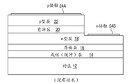
Fig. 1 explained at US6, flip-chip III group-III nitride device in greater detail in 194,742.The row beginning on the 3rd hurdle the 41st, describe device illustrated in fig. 1 as follows: " boundary layer 16 is added to light-emitting diode or laser diode structure to carry out the task of strain engineering and impurity absorption.Be doped with the Al of Mg, Zn, Cd
xIn
yGa
1-x-yN layer (0≤x≤1,0≤y≤1) can be used for this boundary layer.Replacedly, when using Al
xIn
yGa
1-x-yN (x>0) time, this boundary layer can be unadulterated.Boundary layer also can comprise the alloy of AlInGaN, AlInGaP and AlInGaAs and the alloy of GaN, GaP and GaAs.Before growing n-type (GaN:Si) layer 18, active area 10 and p type layer 22, boundary layer 16 directly is deposited on resilient coating 14 tops.The thickness of boundary layer changes at 0.01 –, 10.0 mu m ranges, and preferred thickness range is 0.25 –, 1.0 μ m.Resilient coating 14 is formed at substrate 12 tops.Substrate 12 can be transparent.Metal contact layer 24A, 24B deposit to p type layer and n type layer 22,18 respectively." the preferred embodiment uses GaN:Mg and/or the AlGaN component as boundary layer.
Summary of the invention
The objective of the invention is in III group-III nitride device, to comprise the curvature key-course.In certain embodiments, the curvature key-course can reduce to be grown in the crooked quantity in the III nitride films on the Sapphire Substrate.
Embodiments of the invention comprise a kind of semiconductor structure, and it comprises the III group-III nitride luminescent layer that is arranged between n type district and the p type district.This semiconductor structure further comprises the curvature key-course that is grown on the ground floor.This curvature key-course is arranged between this n type district and this ground floor.This curvature key-course has the theoretical a lattice constant littler than the theoretical a lattice constant of GaN.This ground floor is single crystalline layer basically.
Description of drawings
Fig. 1 explains III group-III nitride light-emitting device, and it has the boundary layer that is arranged between resilient coating and the n type layer.
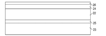
Fig. 2 explanation is according to the part of the III group-III nitride light-emitting device of the embodiment of the invention.
Fig. 3 explanation is connected to the flip-chip light emitting device of base.
Embodiment
III group-III nitride device often is grown on the Sapphire Substrate.The ground floor that is grown on the sapphire comprises any resilient coating or the nucleating layer and the first high-quality single crystalline layer basically, and this ground floor often is GaN.Because lattice and chemical mismatch between GaN and the sapphire are grown in the GaN development stress on the sapphire.Stress quantity can depend on nucleation and merging condition.After this semiconductor structure of growth, along with wafer cooling since with sapphire (7.5x10
-6/ K) less thermal coefficient of expansion (the 5.6x10 of GaN by contrast
-6/ K) reason, additional stress is formed in this semiconductor structure.The stress that during cooling occurs can partly be offset because the natural stress that lattice and chemical mismatch cause.
Along with the thickness that is grown in the semi-conducting material on the sapphire increases, wafer can be crooked with the compression in compensation semiconductor's material partly, make that when from the top, i.e. when semiconductor structure growth surface was on it watched, wafer was protruding.For example, the wafer of device with semiconductor structure of about several micron thick can be crooked about tens microns, wherein should bending represent the difference between Waffer edge height and the central height.Bending is problematic, because during the technology such as photoetching, crooked quantity must be compensated.
According to embodiments of the invention, in III group-III nitride light-emitting device, comprise the layer of compensated bend at least in part.
Fig. 2 explanation is according to the part of the III group-III nitride device of the embodiment of the invention.In the device of Fig. 2 explanation, GaN structure 23 at first is grown on the growth substrates (not shown among Fig. 2), and this growth substrates can be that any suitable growth substrates and this growth substrates typically are sapphire or SiC.GaN structure 23 can comprise one or more preparation layers, such as resilient coating or nucleating layer.At least one high-quality single crystalline layer is comprised in the GaN structure 23, and this single crystalline layer often is the AlGaN at the GaN of high growth temperature or low AlN component.GaN structure 23 can comprise the III group iii nitride layer that is not GaN, such as InGaN, AlGaN or AlInGaN layer.
Curvature key-course 25 is grown in the single crystalline layer top that comprises in the GaN structure 23.Curvature key-course 25 is a single crystalline layer, and its theoretical a lattice constant is less than the actual a lattice constant of curvature key-course growth single crystalline layer on it.In certain embodiments, curvature key-course 25 has the theoretical a lattice constant littler than the theoretical a lattice constant of GaN.In certain embodiments, curvature key-course 25 is AlGaN or AlInGaN.When curvature key-course 25 is grown in GaN or theoretical lattice constant some other material (such as AlGaN with less AlN component) last time bigger than curvature key-course 25, curvature key-course 25 receives tension force.Tension force in the curvature key-course 25 can compensate at least in part in the GaN structure 23 because the thermal stress by the substrate induction that causes from the growth temperature cooling, thereby reduce the crooked quantity in the wafer of device.In the device that does not have the curvature key-course, the inventor observes the bending of 94 μ m.In the comparable device of the AlGaN curvature key-course with 8.5%AlN, the inventor observes the bending of 61 μ m.
In order to make curvature key-course 25 receive tension force, the curvature key-course must be grown on the enough high-quality layer, make the curvature key-course this as single crystalline layer basically.In the device of Fig. 1 explanation, boundary layer 16 directly is deposited on the resilient coating 14, and this resilient coating typically is the unformed layer at low-temperature epitaxy.Like US6, the boundary layer of describing in 194,742 16 that is grown on the resilient coating will not be strained pseudomorphic layer typically, and strained pseudomorphic layer is essential for this layer reduces bending.
AlN component in the AlGaN curvature key-course 25 can be for example in certain embodiments less than 30%; In certain embodiments between 2% and 15%; In certain embodiments between 6% and 10%; Between 7% and 9%, in certain embodiments be 7.5% in certain embodiments, and be 8.5% in certain embodiments.Greater than 10% component, the inventor observes the cracking of burying in the curvature key-course in some devices, and in fact this increased crooked quantity.In certain embodiments, the AlN component in the AlInGaN curvature key-course 25 can be identical with the AlN component of aforesaid AlGaN curvature key-course.Because the lattice constant of InN greater than the lattice constant of GaN, is added the quantity that InN will reduce tension force in the curvature key-course by contrast, thereby the InN component keeps little usually.For example, in certain embodiments, the InN component in the AlInGaN curvature key-course can be the magnitude of several percentages.In certain embodiments, the AlN component in the AlInGaN curvature key-course can reduce thereby compensate the tension force that is caused by interpolation InN at least in part greater than the AlN component of aforesaid AlGaN curvature key-course.
In certain embodiments can be according to the Vegard law between 3.111 and 3.189 from the theoretical lattice constant of the curvature key-course 25 of a lattice constant calculating of AlN (3.111), GaN (3.189), InN (3.533); In certain embodiments can be between 3.165 and 3.188; In certain embodiments can be between 3.180 and 3.184, and in certain embodiments can be between 3.182 and 3.183.For Al
xIn
yGa
1-x-yThe N layer can be according to a
AlInGaN=(a
AlN) x+ (a
InN) y+ (a
GaN) (1-x-y) calculate lattice constant.
Reduce bending thereby curvature key-course 25 is enough thick to form enough tension force, make the curvature key-course not ftracture but enough approach.Thereby the curvature key-course can be thick in certain embodiments for example 200 be lower than the cracking limit just, and is thick in certain embodiments 500 to 1500, thick in certain embodiments 0.5 to 5 μ m, and thick in certain embodiments 1 to 2 μ m.Along with the component increase of AlN in the AlGaN layer, theoretical lattice constant reduces.Therefore, along with the AlN component increases, the thickness that does not have cracking that the AlGaN layer can grow into reduces.
The quantity of tension force in the curvature key-course; Therefore and the curvature key-course reduces crooked ability, for the theoretical lattice constant of the thickness of curvature key-course and curvature key-course and the growth of curvature key-course on it layer the actual lattice constant between the product of the strain that causes of difference.In order to realize prescribed tension quantity, highly strained curvature key-course can be thinner than strained less curvature key-course.In certain embodiments, the curvature key-course is grown on the GaN layer.Actual interior lattice constant of this GaN layer can depend on growth conditions, and can for example between 3.184 and 3.189, change.Have the situation of lattice constant in the comparison facet for curvature key-course growth GaN layer on it, the AlN component of curvature key-course and/or thickness can have the situation of bigger interior lattice constant less than curvature key-course growth GaN layer on it.
In certain embodiments, curvature key-course growth rate is slower than GaN structure 23.
Normally involuntary doping of curvature key-course 25, but it also can use n type or p type dopant to mix.
The semiconductor structure that comprises n type district, luminous zone or active area and p type district is grown in curvature key-course top.N type district 22 at first is grown in the substrate top.N type district 22 can comprise a plurality of layers of different components and concentration of dopant, and for example said a plurality of layers comprise: preparation layer, and such as resilient coating or nucleating layer, it can be n type or involuntary doping; Releasing layer, it is designed to help discharge after a while growth substrates or attenuate semiconductor structure after substrate removal; And n or even p type device layer, it is launched the desired concrete optics of light or electrical properties efficiently to the luminous zone and designs.
In certain embodiments, curvature key-course 25 be interposed in two high-quality basically between the single crystalline layer.In certain embodiments, insert and put curvature key-course 25 two layers one of them or the two in dislocation density can be between 10
5With 10
9Cm
-2
Luminous zone or active area 24 are grown in 22 tops, n type district.The example of suitable luminous zone comprises single thick or thin luminescent layer, perhaps comprises the multiple quantum well light emitting district by a plurality of thin or thick mqw light emitting layer of building layer separation.For example, the multiple quantum well light emitting district can comprise a plurality of luminescent layers of separating by building, and each light emitting layer thickness is 25 or littler, and each barrier thickness is 100 or littler.In certain embodiments, the thickness of each luminescent layer in the device is greater than 50.
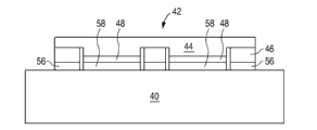
Fig. 3 explanation is connected to the LED 42 of base 40.P contact 48 often for the contact of reflection silver, is formed in the p type district.Before or after forming the p contact, the n type district of exposed portions serve through etching away p type district partly and luminous zone.The semiconductor structure that comprises n type district 22, luminous zone 24 and p type district 26 is represented with structure 44 in Fig. 3.N contact 46 is formed on the exposed portions serve in n type district.Because n contact 46 is formed in the n type district 22, curvature key-course 25 is not arranged in the current path of device and the therefore electrical properties of modifier not, and irrelevant with the component of curvature key-course 25.
During combination of ultrasound, LED tube core 42 places on the base 40.Joint head places on the upper surface of LED tube core, for the III group-III nitride device situation that is grown on the sapphire, often places the upper surface of sapphire growth substrate.Joint head is connected to ultrasonic transducer.Ultrasonic transducer can be the lamination of lead zirconate titanate (PZT) layer for example.When being applied to transducer, transducer begins vibration with the frequency that causes the harmonious resonance of this system (often be tens or the frequency of hundreds of kHz magnitude) when voltage, this so that cause joint head and the LED tube core vibrates, vibration amplitude often is several micron dimensions.Vibration causes atom and the structure counterdiffusion on the base 40 in the metal lattice of the structure on the LED 42, thereby forms continuous joint on the metallurgy.During combining, can add heat and/or pressure.
After LED tube core 42 was attached to base 40, semiconductor growth layer growth substrates on it can be removed, and for example perhaps was suitable for any other technology of concrete growth substrates through laser lift-off, etching.After removing growth substrates, semiconductor structure can be thinned, for example through the Optical Electro-Chemistry etching, and/or the surface can for example utilize photon crystal structure by roughening or patterning.All or GaN structure partly 23 can be retained in the device with curvature key-course 25, perhaps after removing growth substrates, during attenuate, can be removed.After substrate removal, lens, material for transformation of wave length or other structure as known in the art can be arranged in LED 42 tops.
Described the present invention in detail, it will be understood by those skilled in the art that in view of present disclosure, can adjust and do not deviate from the spirit of inventive concept described herein the present invention.Therefore, scope of the present invention does not plan to be subject to specific embodiment illustrated and description.
Claims (15)
1. device comprises:
Semiconductor structure, this semiconductor structure comprises:
Be arranged in the III group-III nitride luminescent layer between n type district and the p type district; And
Be grown in the curvature key-course on the ground floor, wherein:
This curvature key-course has the theoretical a lattice constant littler than the theoretical a lattice constant of GaN;
This ground floor is single crystalline layer basically; And
This curvature key-course is arranged between this n type district and this ground floor.
2. the device of claim 1, wherein this curvature key-course comprises aluminium.
3. the device of claim 1, wherein this curvature key-course is AlGaN.
4. the device of claim 3, wherein this curvature key-course has greater than 0% and less than 10% AlN component.
5. the device of claim 1, wherein this curvature key-course is AlInGaN.
6. the device of claim 1, wherein this curvature key-course has the theoretical a lattice constant between 3.165 and 3.188.
7. the device of claim 1, wherein this curvature key-course has the theoretical a lattice constant between 3.180 and 3.184.
8. the device of claim 1, wherein this curvature key-course thickness is between 0.5 and 5 μ m.
9. the device of claim 1, wherein this curvature key-course thickness is between 1 and 2 μ m.
10. the device of claim 1, wherein this curvature key-course is involuntary doping.
11. the device of claim 1 further comprises the n contact that is arranged in this n type district and contacts with p on being arranged in this p type district, wherein n contacts with p on the two same side that is formed at this semiconductor structure.
12. the device of claim 1, wherein the component of this curvature key-course and thickness are selected the thermal stress of responding to this ground floor from the growth temperature cooling period that promotes to compensate at least in part.
13. a method comprises:
Growing semiconductor structure on substrate, this semiconductor structure comprises:
Be grown in the curvature key-course on the ground floor; And
Be arranged in the III group-III nitride luminescent layer between n type district and the p type district; Wherein:
This curvature key-course has the theoretical a lattice constant littler than the theoretical a lattice constant of GaN;
This ground floor is single crystalline layer basically; And
This curvature key-course is arranged between this n type district and this ground floor.
14. the method for claim 13, wherein this curvature key-course growth rate is slower than this ground floor.
15. the method for claim 13, wherein the component of this curvature key-course and thickness are selected the thermal stress of responding to this ground floor from the growth temperature cooling period that promotes to compensate at least in part.
Applications Claiming Priority (3)
| Application Number | Priority Date | Filing Date | Title |
|---|---|---|---|
| US12/555000 | 2009-09-08 | ||
| US12/555,000 US20110057213A1 (en) | 2009-09-08 | 2009-09-08 | Iii-nitride light emitting device with curvat1jre control layer |
| PCT/IB2010/053537 WO2011030238A1 (en) | 2009-09-08 | 2010-08-04 | Iii-nitride light emitting device with curvature control layer |
Publications (1)
| Publication Number | Publication Date |
|---|---|
| CN102484178A true CN102484178A (en) | 2012-05-30 |
Family
ID=43128314
Family Applications (1)
| Application Number | Title | Priority Date | Filing Date |
|---|---|---|---|
| CN2010800399971A Pending CN102484178A (en) | 2009-09-08 | 2010-08-04 | III-nitride light emitting device with curvature control layer |
Country Status (7)
| Country | Link |
|---|---|
| US (2) | US20110057213A1 (en) |
| EP (1) | EP2476144A1 (en) |
| JP (1) | JP2013504197A (en) |
| KR (1) | KR20120068900A (en) |
| CN (1) | CN102484178A (en) |
| TW (1) | TW201117418A (en) |
| WO (1) | WO2011030238A1 (en) |
Cited By (3)
| Publication number | Priority date | Publication date | Assignee | Title |
|---|---|---|---|---|
| CN107275425A (en) * | 2013-01-31 | 2017-10-20 | 欧司朗光电半导体有限公司 | Layer sequence and the method for manufacturing layer sequence |
| CN107408933A (en) * | 2014-10-03 | 2017-11-28 | 芬兰国家技术研究中心股份公司 | Temperature-compensating compound resonator |
| CN108054260A (en) * | 2017-10-25 | 2018-05-18 | 华灿光电(浙江)有限公司 | The epitaxial wafer and preparation method of a kind of light emitting diode |
Families Citing this family (5)
| Publication number | Priority date | Publication date | Assignee | Title |
|---|---|---|---|---|
| US20130082274A1 (en) * | 2011-09-29 | 2013-04-04 | Bridgelux, Inc. | Light emitting devices having dislocation density maintaining buffer layers |
| JP5166594B1 (en) | 2011-12-12 | 2013-03-21 | 株式会社東芝 | Semiconductor light emitting device |
| US9136430B2 (en) * | 2012-08-09 | 2015-09-15 | Samsung Electronics Co., Ltd. | Semiconductor buffer structure, semiconductor device including the same, and method of manufacturing semiconductor device using semiconductor buffer structure |
| CN108281378B (en) * | 2012-10-12 | 2022-06-24 | 住友电气工业株式会社 | Group III nitride composite substrate, semiconductor device, and methods for manufacturing group III nitride composite substrate and semiconductor device |
| KR102211486B1 (en) * | 2018-12-24 | 2021-02-02 | 한국세라믹기술원 | Manufacturing method of free standing gallium nitride using electrochemical etching method and photoelectric electrode for water decomposition gydrogen production including the same |
Citations (3)
| Publication number | Priority date | Publication date | Assignee | Title |
|---|---|---|---|---|
| US6194742B1 (en) * | 1998-06-05 | 2001-02-27 | Lumileds Lighting, U.S., Llc | Strain engineered and impurity controlled III-V nitride semiconductor films and optoelectronic devices |
| US6927426B2 (en) * | 2002-06-19 | 2005-08-09 | Nippon Telegraph And Telephone Corporation | Semiconductor light-emitting device for optical communications |
| US6996150B1 (en) * | 1994-09-14 | 2006-02-07 | Rohm Co., Ltd. | Semiconductor light emitting device and manufacturing method therefor |
Family Cites Families (7)
| Publication number | Priority date | Publication date | Assignee | Title |
|---|---|---|---|---|
| US5670798A (en) * | 1995-03-29 | 1997-09-23 | North Carolina State University | Integrated heterostructures of Group III-V nitride semiconductor materials including epitaxial ohmic contact non-nitride buffer layer and methods of fabricating same |
| JPH0964477A (en) * | 1995-08-25 | 1997-03-07 | Toshiba Corp | Semiconductor light emitting element and its manufacture |
| JPH10150245A (en) * | 1996-11-21 | 1998-06-02 | Matsushita Electric Ind Co Ltd | Manufacture of gallium nitride semiconductor |
| JP2002261033A (en) * | 2000-12-20 | 2002-09-13 | Matsushita Electric Ind Co Ltd | Manufacturing method of semiconductor and semiconductor substrate, and semiconductor light- emitting device |
| JP3866540B2 (en) * | 2001-07-06 | 2007-01-10 | 株式会社東芝 | Nitride semiconductor device and manufacturing method thereof |
| KR100906164B1 (en) * | 2004-11-18 | 2009-07-03 | 쇼와 덴코 가부시키가이샤 | Gallium nitride-based semiconductor stacked structure, method for fabrication thereof, gallium nitride-based semiconductor device and lamp using the device |
| US7795050B2 (en) * | 2005-08-12 | 2010-09-14 | Samsung Electronics Co., Ltd. | Single-crystal nitride-based semiconductor substrate and method of manufacturing high-quality nitride-based light emitting device by using the same |
-
2009
- 2009-09-08 US US12/555,000 patent/US20110057213A1/en not_active Abandoned
-
2010
- 2010-08-04 CN CN2010800399971A patent/CN102484178A/en active Pending
- 2010-08-04 KR KR1020127008995A patent/KR20120068900A/en not_active Application Discontinuation
- 2010-08-04 EP EP10749916A patent/EP2476144A1/en not_active Withdrawn
- 2010-08-04 WO PCT/IB2010/053537 patent/WO2011030238A1/en active Application Filing
- 2010-08-04 JP JP2012527410A patent/JP2013504197A/en active Pending
- 2010-08-06 TW TW099126371A patent/TW201117418A/en unknown
-
2012
- 2012-06-29 US US13/537,107 patent/US20120264248A1/en not_active Abandoned
Patent Citations (3)
| Publication number | Priority date | Publication date | Assignee | Title |
|---|---|---|---|---|
| US6996150B1 (en) * | 1994-09-14 | 2006-02-07 | Rohm Co., Ltd. | Semiconductor light emitting device and manufacturing method therefor |
| US6194742B1 (en) * | 1998-06-05 | 2001-02-27 | Lumileds Lighting, U.S., Llc | Strain engineered and impurity controlled III-V nitride semiconductor films and optoelectronic devices |
| US6927426B2 (en) * | 2002-06-19 | 2005-08-09 | Nippon Telegraph And Telephone Corporation | Semiconductor light-emitting device for optical communications |
Cited By (5)
| Publication number | Priority date | Publication date | Assignee | Title |
|---|---|---|---|---|
| CN107275425A (en) * | 2013-01-31 | 2017-10-20 | 欧司朗光电半导体有限公司 | Layer sequence and the method for manufacturing layer sequence |
| CN107275425B (en) * | 2013-01-31 | 2019-10-15 | 欧司朗光电半导体有限公司 | Layer sequence and method for manufacturing layer sequence |
| CN107408933A (en) * | 2014-10-03 | 2017-11-28 | 芬兰国家技术研究中心股份公司 | Temperature-compensating compound resonator |
| CN107408933B (en) * | 2014-10-03 | 2020-11-20 | 芬兰国家技术研究中心股份公司 | Temperature compensation composite resonator |
| CN108054260A (en) * | 2017-10-25 | 2018-05-18 | 华灿光电(浙江)有限公司 | The epitaxial wafer and preparation method of a kind of light emitting diode |
Also Published As
| Publication number | Publication date |
|---|---|
| KR20120068900A (en) | 2012-06-27 |
| JP2013504197A (en) | 2013-02-04 |
| US20120264248A1 (en) | 2012-10-18 |
| US20110057213A1 (en) | 2011-03-10 |
| TW201117418A (en) | 2011-05-16 |
| EP2476144A1 (en) | 2012-07-18 |
| WO2011030238A1 (en) | 2011-03-17 |
Similar Documents
| Publication | Publication Date | Title |
|---|---|---|
| US8106403B2 (en) | III-nitride light emitting device incorporation boron | |
| CN102484178A (en) | III-nitride light emitting device with curvature control layer | |
| CN102714256A (en) | Semiconductor light emitting device with layer compensating for the thermal expansion of the substrate | |
| US8945975B2 (en) | Light emitting device grown on a relaxed layer | |
| US9012250B2 (en) | Controlling pit formation in a III-nitride device | |
| KR101810711B1 (en) | Composite growth substrate for growing a semiconductor device |
Legal Events
| Date | Code | Title | Description |
|---|---|---|---|
| C06 | Publication | ||
| PB01 | Publication | ||
| C10 | Entry into substantive examination | ||
| SE01 | Entry into force of request for substantive examination | ||
| C02 | Deemed withdrawal of patent application after publication (patent law 2001) | ||
| WD01 | Invention patent application deemed withdrawn after publication |
Application publication date: 20120530 |