CN102637708A - Solid-state image pickup apparatus, method for manufacturing solid-state image pickup apparatus, and image pickup system - Google Patents
Solid-state image pickup apparatus, method for manufacturing solid-state image pickup apparatus, and image pickup system Download PDFInfo
- Publication number
- CN102637708A CN102637708A CN2012100279294A CN201210027929A CN102637708A CN 102637708 A CN102637708 A CN 102637708A CN 2012100279294 A CN2012100279294 A CN 2012100279294A CN 201210027929 A CN201210027929 A CN 201210027929A CN 102637708 A CN102637708 A CN 102637708A
- Authority
- CN
- China
- Prior art keywords
- dielectric film
- film
- image pickup
- photoelectric conversion
- pickup apparatus
- Prior art date
- Legal status (The legal status is an assumption and is not a legal conclusion. Google has not performed a legal analysis and makes no representation as to the accuracy of the status listed.)
- Pending
Links
- 238000000034 method Methods 0.000 title claims abstract description 39
- 238000004519 manufacturing process Methods 0.000 title abstract description 5
- 239000004065 semiconductor Substances 0.000 claims abstract description 90
- 238000005530 etching Methods 0.000 claims abstract description 70
- 238000006243 chemical reaction Methods 0.000 claims abstract description 63
- 239000000758 substrate Substances 0.000 claims abstract description 44
- VYPSYNLAJGMNEJ-UHFFFAOYSA-N Silicium dioxide Chemical compound O=[Si]=O VYPSYNLAJGMNEJ-UHFFFAOYSA-N 0.000 claims description 86
- HQVNEWCFYHHQES-UHFFFAOYSA-N silicon nitride Chemical compound N12[Si]34N5[Si]62N3[Si]51N64 HQVNEWCFYHHQES-UHFFFAOYSA-N 0.000 claims description 55
- 229910052581 Si3N4 Inorganic materials 0.000 claims description 53
- 239000000377 silicon dioxide Substances 0.000 claims description 30
- 230000003667 anti-reflective effect Effects 0.000 claims description 22
- 239000000463 material Substances 0.000 claims description 20
- 230000004888 barrier function Effects 0.000 claims description 19
- 239000010410 layer Substances 0.000 description 69
- 230000002093 peripheral effect Effects 0.000 description 49
- 239000011229 interlayer Substances 0.000 description 31
- 230000005540 biological transmission Effects 0.000 description 25
- 229910021332 silicide Inorganic materials 0.000 description 22
- FVBUAEGBCNSCDD-UHFFFAOYSA-N silicide(4-) Chemical compound [Si-4] FVBUAEGBCNSCDD-UHFFFAOYSA-N 0.000 description 22
- 229910052814 silicon oxide Inorganic materials 0.000 description 22
- 229920002120 photoresistant polymer Polymers 0.000 description 19
- 230000015572 biosynthetic process Effects 0.000 description 18
- 239000004020 conductor Substances 0.000 description 15
- 229910052751 metal Inorganic materials 0.000 description 15
- 239000002184 metal Substances 0.000 description 15
- 238000005268 plasma chemical vapour deposition Methods 0.000 description 15
- 239000007789 gas Substances 0.000 description 14
- 229920005591 polysilicon Polymers 0.000 description 13
- 230000035945 sensitivity Effects 0.000 description 13
- 229910021420 polycrystalline silicon Inorganic materials 0.000 description 12
- XUIMIQQOPSSXEZ-UHFFFAOYSA-N Silicon Chemical compound [Si] XUIMIQQOPSSXEZ-UHFFFAOYSA-N 0.000 description 11
- 229910052710 silicon Inorganic materials 0.000 description 11
- 239000010703 silicon Substances 0.000 description 11
- XKRFYHLGVUSROY-UHFFFAOYSA-N Argon Chemical compound [Ar] XKRFYHLGVUSROY-UHFFFAOYSA-N 0.000 description 10
- 239000012535 impurity Substances 0.000 description 9
- 230000000694 effects Effects 0.000 description 8
- 230000008859 change Effects 0.000 description 7
- 238000010276 construction Methods 0.000 description 7
- 238000000151 deposition Methods 0.000 description 7
- 230000008021 deposition Effects 0.000 description 7
- 238000009792 diffusion process Methods 0.000 description 7
- 238000005516 engineering process Methods 0.000 description 7
- IJGRMHOSHXDMSA-UHFFFAOYSA-N Atomic nitrogen Chemical compound N#N IJGRMHOSHXDMSA-UHFFFAOYSA-N 0.000 description 6
- 230000014509 gene expression Effects 0.000 description 6
- 239000011261 inert gas Substances 0.000 description 6
- 238000002955 isolation Methods 0.000 description 6
- 239000003595 mist Substances 0.000 description 6
- 230000004048 modification Effects 0.000 description 6
- 238000012986 modification Methods 0.000 description 6
- 230000003287 optical effect Effects 0.000 description 6
- 229910052786 argon Inorganic materials 0.000 description 5
- 238000010586 diagram Methods 0.000 description 5
- 238000001020 plasma etching Methods 0.000 description 5
- QGZKDVFQNNGYKY-UHFFFAOYSA-N Ammonia Chemical compound N QGZKDVFQNNGYKY-UHFFFAOYSA-N 0.000 description 4
- NBVXSUQYWXRMNV-UHFFFAOYSA-N fluoromethane Chemical compound FC NBVXSUQYWXRMNV-UHFFFAOYSA-N 0.000 description 4
- 150000002500 ions Chemical class 0.000 description 4
- 238000005036 potential barrier Methods 0.000 description 4
- 230000009467 reduction Effects 0.000 description 4
- 230000003321 amplification Effects 0.000 description 3
- QVGXLLKOCUKJST-UHFFFAOYSA-N atomic oxygen Chemical compound [O] QVGXLLKOCUKJST-UHFFFAOYSA-N 0.000 description 3
- 239000010941 cobalt Substances 0.000 description 3
- 229910017052 cobalt Inorganic materials 0.000 description 3
- GUTLYIVDDKVIGB-UHFFFAOYSA-N cobalt atom Chemical compound [Co] GUTLYIVDDKVIGB-UHFFFAOYSA-N 0.000 description 3
- 238000007667 floating Methods 0.000 description 3
- 229940090044 injection Drugs 0.000 description 3
- 238000002347 injection Methods 0.000 description 3
- 239000007924 injection Substances 0.000 description 3
- 229910052757 nitrogen Inorganic materials 0.000 description 3
- 238000003199 nucleic acid amplification method Methods 0.000 description 3
- 239000001301 oxygen Substances 0.000 description 3
- 229910052760 oxygen Inorganic materials 0.000 description 3
- 238000000059 patterning Methods 0.000 description 3
- 230000008569 process Effects 0.000 description 3
- WFKWXMTUELFFGS-UHFFFAOYSA-N tungsten Chemical compound [W] WFKWXMTUELFFGS-UHFFFAOYSA-N 0.000 description 3
- 239000010937 tungsten Substances 0.000 description 3
- 229910052721 tungsten Inorganic materials 0.000 description 3
- RYGMFSIKBFXOCR-UHFFFAOYSA-N Copper Chemical compound [Cu] RYGMFSIKBFXOCR-UHFFFAOYSA-N 0.000 description 2
- BLRPTPMANUNPDV-UHFFFAOYSA-N Silane Chemical compound [SiH4] BLRPTPMANUNPDV-UHFFFAOYSA-N 0.000 description 2
- RTAQQCXQSZGOHL-UHFFFAOYSA-N Titanium Chemical compound [Ti] RTAQQCXQSZGOHL-UHFFFAOYSA-N 0.000 description 2
- NRTOMJZYCJJWKI-UHFFFAOYSA-N Titanium nitride Chemical compound [Ti]#N NRTOMJZYCJJWKI-UHFFFAOYSA-N 0.000 description 2
- 229910021529 ammonia Inorganic materials 0.000 description 2
- 238000000429 assembly Methods 0.000 description 2
- 230000000712 assembly Effects 0.000 description 2
- 239000010949 copper Substances 0.000 description 2
- 229910052802 copper Inorganic materials 0.000 description 2
- 230000002950 deficient Effects 0.000 description 2
- 230000002349 favourable effect Effects 0.000 description 2
- 238000010438 heat treatment Methods 0.000 description 2
- QJGQUHMNIGDVPM-UHFFFAOYSA-N nitrogen group Chemical group [N] QJGQUHMNIGDVPM-UHFFFAOYSA-N 0.000 description 2
- 238000001259 photo etching Methods 0.000 description 2
- 238000002360 preparation method Methods 0.000 description 2
- 229910000077 silane Inorganic materials 0.000 description 2
- 239000010936 titanium Substances 0.000 description 2
- 229910052719 titanium Inorganic materials 0.000 description 2
- 240000001439 Opuntia Species 0.000 description 1
- BOTDANWDWHJENH-UHFFFAOYSA-N Tetraethyl orthosilicate Chemical compound CCO[Si](OCC)(OCC)OCC BOTDANWDWHJENH-UHFFFAOYSA-N 0.000 description 1
- AZDRQVAHHNSJOQ-UHFFFAOYSA-N alumane Chemical group [AlH3] AZDRQVAHHNSJOQ-UHFFFAOYSA-N 0.000 description 1
- 239000003990 capacitor Substances 0.000 description 1
- 238000005229 chemical vapour deposition Methods 0.000 description 1
- 238000001514 detection method Methods 0.000 description 1
- 230000002708 enhancing effect Effects 0.000 description 1
- 239000001307 helium Substances 0.000 description 1
- 229910052734 helium Inorganic materials 0.000 description 1
- SWQJXJOGLNCZEY-UHFFFAOYSA-N helium atom Chemical compound [He] SWQJXJOGLNCZEY-UHFFFAOYSA-N 0.000 description 1
- 239000000203 mixture Substances 0.000 description 1
- 150000004767 nitrides Chemical class 0.000 description 1
- 239000003921 oil Substances 0.000 description 1
- 230000003647 oxidation Effects 0.000 description 1
- 238000007254 oxidation reaction Methods 0.000 description 1
- 238000005375 photometry Methods 0.000 description 1
- 238000005498 polishing Methods 0.000 description 1
- 238000003825 pressing Methods 0.000 description 1
- 230000000644 propagated effect Effects 0.000 description 1
- 230000003252 repetitive effect Effects 0.000 description 1
- 239000011347 resin Substances 0.000 description 1
- 229920005989 resin Polymers 0.000 description 1
- 230000000717 retained effect Effects 0.000 description 1
- 238000004544 sputter deposition Methods 0.000 description 1
- 230000001629 suppression Effects 0.000 description 1
- CZDYPVPMEAXLPK-UHFFFAOYSA-N tetramethylsilane Chemical compound C[Si](C)(C)C CZDYPVPMEAXLPK-UHFFFAOYSA-N 0.000 description 1
- 229910021341 titanium silicide Inorganic materials 0.000 description 1
- 239000012780 transparent material Substances 0.000 description 1
- PQDJYEQOELDLCP-UHFFFAOYSA-N trimethylsilane Chemical compound C[SiH](C)C PQDJYEQOELDLCP-UHFFFAOYSA-N 0.000 description 1
- 229940094989 trimethylsilane Drugs 0.000 description 1
- WQJQOUPTWCFRMM-UHFFFAOYSA-N tungsten disilicide Chemical compound [Si]#[W]#[Si] WQJQOUPTWCFRMM-UHFFFAOYSA-N 0.000 description 1
- 229910021342 tungsten silicide Inorganic materials 0.000 description 1
Images


Classifications
-
- H—ELECTRICITY
- H01—ELECTRIC ELEMENTS
- H01L—SEMICONDUCTOR DEVICES NOT COVERED BY CLASS H10
- H01L27/00—Devices consisting of a plurality of semiconductor or other solid-state components formed in or on a common substrate
- H01L27/14—Devices consisting of a plurality of semiconductor or other solid-state components formed in or on a common substrate including semiconductor components sensitive to infrared radiation, light, electromagnetic radiation of shorter wavelength or corpuscular radiation and specially adapted either for the conversion of the energy of such radiation into electrical energy or for the control of electrical energy by such radiation
- H01L27/144—Devices controlled by radiation
- H01L27/146—Imager structures
- H01L27/14683—Processes or apparatus peculiar to the manufacture or treatment of these devices or parts thereof
- H01L27/14685—Process for coatings or optical elements
-
- H—ELECTRICITY
- H01—ELECTRIC ELEMENTS
- H01L—SEMICONDUCTOR DEVICES NOT COVERED BY CLASS H10
- H01L27/00—Devices consisting of a plurality of semiconductor or other solid-state components formed in or on a common substrate
- H01L27/14—Devices consisting of a plurality of semiconductor or other solid-state components formed in or on a common substrate including semiconductor components sensitive to infrared radiation, light, electromagnetic radiation of shorter wavelength or corpuscular radiation and specially adapted either for the conversion of the energy of such radiation into electrical energy or for the control of electrical energy by such radiation
- H01L27/144—Devices controlled by radiation
- H01L27/146—Imager structures
- H01L27/14601—Structural or functional details thereof
- H01L27/14625—Optical elements or arrangements associated with the device
- H01L27/14629—Reflectors
-
- H—ELECTRICITY
- H01—ELECTRIC ELEMENTS
- H01L—SEMICONDUCTOR DEVICES NOT COVERED BY CLASS H10
- H01L27/00—Devices consisting of a plurality of semiconductor or other solid-state components formed in or on a common substrate
- H01L27/14—Devices consisting of a plurality of semiconductor or other solid-state components formed in or on a common substrate including semiconductor components sensitive to infrared radiation, light, electromagnetic radiation of shorter wavelength or corpuscular radiation and specially adapted either for the conversion of the energy of such radiation into electrical energy or for the control of electrical energy by such radiation
- H01L27/144—Devices controlled by radiation
- H01L27/146—Imager structures
- H01L27/14601—Structural or functional details thereof
- H01L27/14632—Wafer-level processed structures
-
- H—ELECTRICITY
- H01—ELECTRIC ELEMENTS
- H01L—SEMICONDUCTOR DEVICES NOT COVERED BY CLASS H10
- H01L27/00—Devices consisting of a plurality of semiconductor or other solid-state components formed in or on a common substrate
- H01L27/14—Devices consisting of a plurality of semiconductor or other solid-state components formed in or on a common substrate including semiconductor components sensitive to infrared radiation, light, electromagnetic radiation of shorter wavelength or corpuscular radiation and specially adapted either for the conversion of the energy of such radiation into electrical energy or for the control of electrical energy by such radiation
- H01L27/144—Devices controlled by radiation
- H01L27/146—Imager structures
- H01L27/14601—Structural or functional details thereof
- H01L27/14641—Electronic components shared by two or more pixel-elements, e.g. one amplifier shared by two pixel elements
-
- H—ELECTRICITY
- H01—ELECTRIC ELEMENTS
- H01L—SEMICONDUCTOR DEVICES NOT COVERED BY CLASS H10
- H01L27/00—Devices consisting of a plurality of semiconductor or other solid-state components formed in or on a common substrate
- H01L27/14—Devices consisting of a plurality of semiconductor or other solid-state components formed in or on a common substrate including semiconductor components sensitive to infrared radiation, light, electromagnetic radiation of shorter wavelength or corpuscular radiation and specially adapted either for the conversion of the energy of such radiation into electrical energy or for the control of electrical energy by such radiation
- H01L27/144—Devices controlled by radiation
- H01L27/146—Imager structures
- H01L27/14683—Processes or apparatus peculiar to the manufacture or treatment of these devices or parts thereof
- H01L27/14687—Wafer level processing
-
- H—ELECTRICITY
- H01—ELECTRIC ELEMENTS
- H01L—SEMICONDUCTOR DEVICES NOT COVERED BY CLASS H10
- H01L27/00—Devices consisting of a plurality of semiconductor or other solid-state components formed in or on a common substrate
- H01L27/14—Devices consisting of a plurality of semiconductor or other solid-state components formed in or on a common substrate including semiconductor components sensitive to infrared radiation, light, electromagnetic radiation of shorter wavelength or corpuscular radiation and specially adapted either for the conversion of the energy of such radiation into electrical energy or for the control of electrical energy by such radiation
- H01L27/144—Devices controlled by radiation
- H01L27/146—Imager structures
- H01L27/14683—Processes or apparatus peculiar to the manufacture or treatment of these devices or parts thereof
- H01L27/14689—MOS based technologies
Abstract
A method for manufacturing a solid-state image pickup device is provided. The image pickup apparatus includes a photoelectric conversion portion disposed on the semiconductor substrate, a first insulating film over the photoelectric conversion portion, functioning as an antireflection film, a second insulating film on the first insulating film, disposed corresponding to the photoelectric conversion portion, and a waveguide having a clad and a core whose bottom is disposed on the second insulating film. The method includes forming an opening by anisotropically etching part of a member disposed over the photoelectric conversion portion, thereby forming the clad, and forming the core in the opening. In the method, the etching is performed under conditions where the etching rate of the second insulating film is lower than the etching rate of the member.
Description
Technical field
The present invention relates to a kind of solid-state image pickup apparatus, comprise the image picking system of this solid-state image pickup apparatus and be used to make the method for this solid-state image pickup apparatus.
Background technology
Amount for the light that increases the photoelectric conversion section that gets into solid-state image pickup apparatus has proposed in solid-state image pickup apparatus, to use waveguide recently.The open No.2006-191000 of Japan Patent discloses in comprising the solid-state image pickup apparatus of waveguide, is used to form the double anti-reflective film on light receiving part of etch stop film of waveguide.
The open No.2008-041726 of Japan Patent discloses pixel portion and has been provided with the etched etch stop film that is used to form contact hole.
Summary of the invention
The present invention provides a kind of method that is used to make solid-state image pickup apparatus; Said solid-state image pickup apparatus comprises photoelectric conversion section, first dielectric film, second dielectric film and waveguide on first dielectric film; Said photoelectric conversion section is arranged in the Semiconductor substrate; Said first dielectric film is as the anti-reflective film on the photoelectric conversion section; Said second dielectric film and photoelectric conversion section are provided with accordingly, and said waveguide has covering (clad) and core, and the bottom of said core is arranged on second dielectric film.Said method comprises that the said parts of condition lower part etching through being etched sooner than second dielectric film at the parts that are arranged on the photoelectric conversion section form opening, thereby forms said covering, and in said opening, forms said core.
Solid-state image pickup apparatus according to an aspect of the present invention comprises a plurality of photoelectric conversion section that are arranged in the Semiconductor substrate.First dielectric film is arranged on the photoelectric conversion section, and as anti-reflective film.A plurality of second dielectric films and photoelectric conversion section are arranged on first dielectric film accordingly.Each second dielectric film is as etch stop film.Said solid-state image pickup apparatus also comprises a plurality of waveguides, and each waveguide comprises covering and core, the bottom of said core and corresponding second dielectric film contact.Said core is by processing with the second dielectric film identical materials.
With reference to the description of accompanying drawing to exemplary embodiment, further characteristic of the present invention will become clear from following.
Description of drawings
Fig. 1 is the circuit diagram of pixel cell of the solid-state image pickup apparatus of first embodiment.
Fig. 2 is the expression that shows the layout in the plane graph of pixel cell of solid-state image pickup apparatus of first embodiment.
Fig. 3 A to Fig. 3 C is the expression of method that is used to make the solid-state image pickup apparatus of first embodiment.
Fig. 4 A to Fig. 4 C is the expression of method that is used to make the solid-state image pickup apparatus of first embodiment.
Fig. 5 A and Fig. 5 B are the expressions of method that is used to make the solid-state image pickup apparatus of first embodiment.
Fig. 6 is the schematic partial section of the solid-state image pickup apparatus of first embodiment.
Fig. 7 is the sketch map of the layout in the plane graph of first embodiment.
Fig. 8 A and Fig. 8 B are the sketch mapes that shows the layout in the plane graph of modification of first embodiment.
Fig. 9 is the schematic sectional view according to the solid-state image pickup apparatus of second embodiment.
Figure 10 is the block diagram of solid-state image pickup apparatus and image picking system.
Figure 11 A to Figure 11 D is the expression that is used to make according to the method for the solid-state image pickup apparatus of the 4th embodiment.
Figure 12 is the schematic partial section according to the solid-state image pickup apparatus of the 5th embodiment.
Figure 13 A to Figure 13 C is the expression of method that is used to make the solid-state image pickup apparatus of the 5th embodiment.
Figure 14 is the schematic partial section according to the solid-state image pickup apparatus of the 6th embodiment.
Figure 15 A and Figure 15 B all are the schematic partial sections according to the solid-state image pickup apparatus of the 7th embodiment.
Figure 16 A to Figure 16 C is the sketch map that is used to make according to the method for the solid-state image pickup apparatus of the 8th embodiment.
Figure 17 A to Figure 17 C is the schematic sectional view that is used to make according to the method for the solid-state image pickup apparatus of the 8th embodiment.
Figure 18 A and Figure 18 B are the schematic sectional view that is used to make according to the method for the solid-state image pickup apparatus of the 8th embodiment.
Figure 19 A and Figure 19 B are the schematic sectional view that is used to make according to the method for the solid-state image pickup apparatus of the 8th embodiment.
Figure 20 A and Figure 20 B are the schematic partial sections of the solid-state image pickup apparatus of the 8th embodiment.
Figure 21 is the schematic sectional view according to the solid-state image pickup apparatus of the 9th embodiment.
Embodiment
Therefore the etch stop film that in the open No.2006-191000 of Japan Patent, is used to form waveguide can, can be made the thickness of etch stop film reduce by partially-etched, and perhaps film can be etched damage.Therefore, the optical property of the etch stop film that serves as anti-reflective film is reduced.
In the open No.2008-041726 of Japan Patent, etch stop film is not used in the etching that in the zone except pixel portion, is used to form contact hole.If some damages take place during etching, then noise can take place, and therefore, reduces picture quality.During the present invention addresses these problems at least one.
The present invention relates to a kind of method that is used to make solid-state image pickup apparatus, said solid-state image pickup apparatus comprises photoelectric conversion section, first dielectric film, second dielectric film and the waveguide that for example is arranged on the Semiconductor substrate.First dielectric film serves as the anti-reflective film on the photoelectric conversion section.Second dielectric film is arranged on first dielectric film, and is corresponding with photoelectric conversion section.Waveguide has covering and core, and the bottom of core is arranged on second dielectric film.In the method that is used for making solid-state image pickup apparatus, form covering through following manner, that is, form opening through the partially-etched parts that are arranged on the photoelectric conversion section, and in said opening, form core.In order to form said opening, be lower than at the etch-rate of second dielectric film under the condition of etch-rate of said parts and carry out etching.This method can prevent the reduction of the optical property of anti-reflective film.
Solid-state image pickup apparatus is included in a plurality of photoelectric conversion section, first dielectric film and a plurality of second dielectric film on the Semiconductor substrate; First dielectric film is as the anti-reflective film on the photoelectric conversion section; Said a plurality of second dielectric film is arranged on first dielectric film, with corresponding with corresponding photoelectric conversion section.Solid-state image pickup apparatus also comprises a plurality of waveguides, and each waveguide comprises covering and core, and core is by processing with the second dielectric film identical materials.The bottom of said core contacts with second dielectric film.Solid-state image pickup apparatus with such structure can show the sensitivity of enhancing.
To describe exemplary embodiment of the present invention with reference to accompanying drawing now.In the following description, with part and step in semi-conductive common structure and the manufacturing approach not being elaborated.In following examples, the refractive index of silicon nitride is higher than the refractive index of silica, and the refractive index of silicon oxynitride is between these refractive indexes.For example, silicon nitride has about refractive index of 1.75 to 2.34, and silica has about refractive index of 1.35 to 1.54.Visible light has the wavelength (Iwanami Rikagaku Jiten, is published by Iwanami Shoten by the 5th edition) in the scope of about 360nm to 830nm.
The opening that this paper mentions can pass interlayer dielectric, perhaps can be the form of not passing the depression of interlayer dielectric, and can be called as the hole.In the following description, the embodiment with waveguide will be described in the structure that has formed opening.Yet opening is not limited thereto purposes.Embodiments of the invention can be widely used in semiconductor device.The etching selectivity that this paper mentions is meant the ratio of etch-rate of etch-rate and second parts of first parts.Along with etching selectivity increases, first parts will be by etching more.On the contrary, along with etching selectivity reduces, second parts will get more than the first parts etching.The same material that this paper mentions is meant the material that contains identical principal component.For example, silicon nitride can have different nitrogen contents, and they are considered to same material in following examples.
First embodiment
To describe the solid-state image pickup apparatus of first embodiment referring to figs. 1 through Fig. 7 and Figure 10 now.Describing at first will be with reference to Fig. 1, Fig. 2, Fig. 7 and Figure 10.
Fig. 1 is the circuit diagram of pixel cell of the solid-state image pickup apparatus of first embodiment.Pixel cell 100 comprises four photodiodes (below be called PD) 101 to 104, four transmission transistors 105 to 108, single reset transistor 110 and single amplifier transistors 112.In addition, floating diffusion node (below be called the FD node) 109 is provided.In the description of first embodiment, signal charge is meant electronics, and transistor is the n type.
Four PD that its anode all is connected with ground 101 to 104 convert incident light into according to the amount of incident light electric charge, and store said electric charge.Four transmission transistors 105 to 108 are separately as the conveyer that will be sent to FD node 109 at signal charge of locating to produce of the correspondence among the PD 101 to 104.More particularly, a PD 101 is connected with the source electrode of first transmission transistor 105, and the 2nd PD 102 is connected with the source electrode of second transmission transistor 106.In addition, the 3rd PD 103 is connected with the source electrode of the 3rd transmission transistor 107, and PD 104 is connected with the source electrode of the 4th transmission transistor 108.The drain electrode of first transmission transistor, 105 to the 4th transmission transistors 108 links together, to limit FD node 109.The gate electrode of amplifier transistor 112 is connected with FD node 109.The drain electrode of amplifier transistor 112 is connected with output signal line 113 with power line 111 respectively with source electrode.Therefore, the signal according to the electromotive force of FD node 109 outputs to output signal line 113.Reset transistor 110 is connected with FD node 109, and the electromotive force of FD node 109 is reset to the electromotive force of expectation.Simultaneously, can be respectively through electric current being put on transmission transistor 105 to 108 PD 101 to 104 that resets.Power line 111 has at least two electromotive forces, can signal be outputed to output signal line 113 through FD node 109 being arranged at two electromotive forces.Output signal line is connected with a plurality of pixels.The terminal of output signal line 113 is connected with reading circuit (describing after a while).
When the repetitive that comprises at least one photoelectric conversion section limited pixel, the pixel cell 100 shown in Fig. 1 had four pixels.Yet the quantity of the pixel in the pixel cell 100 is not limited to four.In addition, pixel cell 100 can comprise selection transistor or capacitor.Though PD serves as photoelectric conversion section in the present embodiment, photogate (photogate) can be used as photoelectric conversion section.
Figure 10 shows the diagram structure of solid-state image pickup apparatus and image picking system.In Figure 10, solid-state image pickup apparatus 1001 comprises pixel portion 1011, vertical scanning circuit 1012, two reading circuits 1013, two horizontal scanning circuits 1014 and two output amplifiers 1015.Zone except pixel portion is called as peripheral circuit part 1016.
In Figure 10, a plurality of pixel cells shown in Fig. 1 are arranged in the pixel portion 1011 with two-dimensional way.In other words, a plurality of pixel arrangement are in pixel portion 1011.Each pixel cell comprises a plurality of pixels.Each reading circuit 1013 comprises for example column amplifier, CDS circuit and adder, and carries out from the amplification and the addition of the signal that is read through the pixel the row of vertical signal line options by vertical scanning circuit 1012.For each pixel column or for every two or more pixel columns, column amplifier, CDS circuit and adder are provided.Each horizontal scanning circuit 1014 produces the signal that is used for successively from reading circuit 1013 read output signals of correspondence.Each output amplifier 1015 amplifies the signal in the row of being selected by horizontal scanning circuit 1014, and the output amplifying signal.This structure only is one of exemplary embodiment of solid-state image pickup apparatus, in other embodiments other structure can be provided.For example, reading circuit 1013, horizontal scanning circuit 1014 and output amplifier 1015 form two outgoing routes, and each outgoing route is arranged on each side of the vertical direction of pixel portion 1011.Yet, in another embodiment, three or more a plurality of outgoing route can be provided.
To describe with reference to the layout in Fig. 2 pair of plane graph corresponding now with Fig. 1.Fig. 2 is the schematic plan view of the layout in the plane graph, and shows the structure of outline projection on the first type surface of the Semiconductor substrate on the first type surface with assembly.In the structure shown in Fig. 2, be provided with a PD 201 to PD 204.For simplicity, Fig. 2 shows the charge storaging area (n type semiconductor region) as the part of PD.The gate electrode 205 to 208 of first transmission transistor to the, four transmission transistors is arranged with a PD 201 to PD 204 respectively accordingly.The drain electrode of first transmission transistor and second transmission transistor is common, and this common region is served as first floating diffusion region 209 (below be called a FD district).The drain electrode of the 3rd transmission transistor and the 4th transmission transistor is common, and this common region is served as second floating diffusion region 210 (below be called the 2nd FD district).The gate electrode 212 of the one FD district 209, the 2nd FD district 210 and amplifier transistor is connected through connecting wiring 213.The gate electrode 212 and the connecting wiring 213 of amplifier transistor are integrally formed.The one FD district 209 is connected with shared contact component (contact) 214 with connecting wiring 213, and FD district 210 is connected with shared contact component 215 with connecting wiring 213.Shared contact component is meant and does not use wiring layer and with semiconductor region and another semiconductor region, with semiconductor region and gate electrode, or contact component that gate electrode is connected with another gate electrode.In Fig. 2, the 2nd FD district 210 is and the source electrode of reset transistor or the common region of drain electrode.Label 211 is specified the gate electrode of reset transistor.
In Fig. 2, having formed PD and intention therein is source area (active region) is arranged as the zone in the zone of transistorized source electrode, drain electrode and raceway groove, and other zone is an element isolation zone 217.Between the PD or have the zone between the gate electrode of the transmission transistor in the source area to be equipped with the potential barrier 216 that is used for signal charge.Potential barrier 216 comprises semiconductor region.Potential barrier 216 is as the element isolation zone of the transportation (traffic) of the signal charge between the control PD.
To describe etch stop film with reference to Fig. 7 now.Fig. 7 be with Fig. 2 in the corresponding plane graph of plane graph in the schematic plan view of layout.The part of Fig. 7 display pixel cells 100a and adjacent pixel unit 100b.In the layout shown in Fig. 7, be provided with dielectric film 701 to 704 as etch stop film.Dielectric film 701 to 704 is arranged with charge storaging area correspondingly.Dielectric film 701 to 704 can be processed by silicon nitride.Dielectric film 701 to 704 all has the big area of area than the optical receiving surface of photoelectric conversion section; And if possible; Arrange that by this way promptly, the outer rim of each dielectric film 701 to 704 is not overlapping with the corresponding charge storaging area 201 to 204 as photoelectric conversion section.This is to be used to form the patterning damage of dielectric film 701 to 704 because such layout can prevent charge storaging area 201 to 204.Therefore, the dielectric film shown in Fig. 7 701 to 704 is arranged to the part of connecting wiring 213 of a part and the adjacent pixel unit 100b of the gate electrode 205 to 208 that covers transmission transistor.This layout can prevent that gate electrode and wiring are used to form the etch damage of opening, will describe said opening after a while.
In addition, dielectric film 701 to 704 be set to not with gate electrode 205-208 on contact component 705 to 708 and the region overlapping that other transistorized contact component is set therein.The formation of this convenient contact component 705 to 708 and other transistorized contact component.
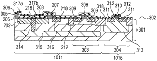
To describe the method that is used to make solid-state image pickup apparatus with reference to Fig. 3 A to Fig. 5 B now.Fig. 3 A to Fig. 5 B is line III, IV, V-III, the IV in Fig. 2, the sectional view of V intercepting, and manufacturing approach is shown.Fig. 3 A to Fig. 5 B shows the 2nd PD and the 3rd PD, the transistor 303 of pixel cell and the cross section of the transistor 304 in the peripheral circuit part of line III in Fig. 2, IV, V-III, IV, V intercepting.These parts are used with above identical label and are specified, and therefore the descriptions thereof are omitted.In addition, with the part that forms through common technique not being described in detail.
At first, will describe being used to prepare the operation that the Semiconductor substrate of element has been set on it with reference to Fig. 3 A.The Semiconductor substrate 301 of preparation is processed by silicon, and had first type surface 302.Semiconductor substrate 301 has charge storaging area 202 and 203, the transistor in pixel portion 303 and the transistor in peripheral circuit part 304 of two PD.In Fig. 3 A, the transistor 303 of pixel cell has N type source/drain regions 309 and gate electrode 308.N type semiconductor district 314 is positioned at below charge storaging area 202 and 203.N type semiconductor district 314 has than charge storaging area 202 and 203 low impurity concentrations, and constitutes the part of photoelectric conversion section.N type semiconductor district 314 is positioned at above the P type semiconductor district 315, and P type semiconductor district 315 is as the part of photoelectric conversion section.In addition, P type semiconductor district 316 is positioned at below the source/drain regions 309 and the 2nd FD district 210 of transistor 303.Transistor 304 in the peripheral circuit part is one of transistors that constitute cmos circuit.The transistor 304 of peripheral circuit part comprises the N type source/drain regions 311 that is formed in the P type semiconductor district 313 and the gate electrode 310 between source/drain regions 311 on the first type surface 302 of Semiconductor substrate.Preparation has the Semiconductor substrate 301 of these elements.Because the element of Semiconductor substrate 301 can form through known method, therefore omit and describe.In each figure, not shown gate insulating film.
Fig. 3 A is presented at the step that forms dielectric film on the element.The order of dielectric film of in pixel portion 1011, processing by the dielectric film (not shown) of being processed by silica, by silicon nitride from first type surface 302 305 and the dielectric film 306 processed by silica forms these dielectric films.These dielectric films can be formed by plasma activated chemical vapour deposition (plasma CVD).
Then, shown in Fig. 3 A, on pixel portion 1011 and peripheral circuit part 1016, form the dielectric film of processing by silicon nitride 307 through low pressure plasma CVD (LP-CVD).Before forming dielectric film 307, can on pixel portion 1011 and peripheral circuit part 1016, form the silicon oxide film (not shown) through plasma CVD.This is that expose at source/drain regions 311 places that prevent the transistor 304 of first type surface 302 in peripheral circuit part 1016 of Semiconductor substrate.
Translate into Fig. 3 B, through known photoetching technique and etching technique pixel portion 1011 and the dielectric film 307 on the peripheral circuit part 1016 are patterned as the shape of expectation, thereby form dielectric film 317 and 318.Dielectric film 317 is arranged on charge storaging area 202 and 203, extends in the zone of the part of the gate electrode of assigning to corresponding transmission transistor from each photoelectric conversion part. Dielectric film 317 and 318 upper surface have the shape of the shape of following corresponding gate electrode.Step shown in Fig. 3 A and Fig. 3 B forms the dielectric film 701 to 704 shown in Fig. 7.Dielectric film 317a shown in Fig. 3 B is corresponding to the dielectric film shown in Fig. 7 702, and the dielectric film 317b shown in Fig. 3 B is corresponding to the dielectric film shown in Fig. 7 703.In pixel portion 1011, remove other part of the dielectric film 307 shown in Fig. 3 A through etching.In peripheral circuit part 1016, the dielectric film 307 among Fig. 3 A is as there not being etched dielectric film 318 to keep.
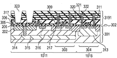
Translate into Fig. 3 C, on the structure shown in Fig. 3 B, form interlayer dielectric 319, contact component 320, first wiring layer 321 and second wiring layer 322 with via conductor (via conductor).Be provided with many wirings of a plurality of contact components and wiring layer.Interlayer dielectric 319 comprises insulating barrier of being processed by silica that is arranged alternately with a mode at another top and the insulating barrier of being processed by silicon nitride.The insulating barrier of being processed by silica forms the thickness of about 120nm to 1000nm separately through plasma CVD.In addition, the insulating barrier of being processed by silicon nitride forms the thickness of about 10nm to 200nm separately through plasma CVD.Therefore, silica occupies the major part of interlayer dielectric 319.Silicon nitride dielectric layer is used to form the etch stop film of wiring layer and via conductor, perhaps with the nonproliferation film that acts on the diffusion that prevents the metal in the wiring layer.The intention of interlayer dielectric 319 is the coverings that form waveguide.
In Fig. 3 C, the silicon nitride dielectric layer that contacts with the upper surface of first wiring layer or second wiring layer is as the nonproliferation film of metal that prevents wiring layer or copper diffusion.On the other hand, the insulating barrier of lower face side that is arranged on first wiring layer and second wiring layer is with acting on the etch stop film that forms first wiring layer and second wiring layer through mosaic technology.Insulating barrier as etch stop film has than the little thickness of insulating barrier as nonproliferation film.In mosaic technology, in insulating barrier, be formed for connecting up, or the groove of wiring and via conductor.In order to form groove through etching, etch stop film is useful for the shape of control groove.Therefore, the lower face side at first wiring layer 321 and second wiring layer 322 provides the insulating barrier as etch stop film.Owing to will remove etch stop film through forming groove; So etch stop film all forms by this way; That is, its lower surface will flush with the lower surface of first wiring layer or second wiring layer, perhaps will be positioned at the horizontal upper of the lower surface of first wiring layer or second wiring layer.Can prepare the wafer that is provided with the structure shown in Fig. 3 in advance, and on said wafer, carry out the following operation that is used to form opening.
Subsequently, will form the structure shown in Fig. 4 A through in the interlayer dielectric shown in Fig. 3 C 319, forming opening 323.On interlayer dielectric 319, be formed on the photoresist pattern (not shown) that has opening in the zone corresponding with photoelectric conversion section, and through using said photoresist pattern to carry out etching as mask.For said etching, carry out anisotropic etching, for example, plasma etching.Remove interlayer dielectric 319 through etching, till exposing dielectric film 317.The intention of dielectric film 317 is to alleviate the damage of etching to photoelectric conversion section, but also as etch stop film.In addition, the first type surface 302 of Semiconductor substrate and the dielectric film between the dielectric film 317, that is, dielectric film (not shown) and dielectric film 305 and 306 by silica is processed are used as for the anti-reflective film that gets into the light in the Semiconductor substrate.The thickness of dielectric film 306 relates to the performance of the anti-reflective film in the sandwich construction.This is because dielectric film 306 causes repeatedly reflection, therefore is used to reduce the reflection between dielectric film 305 and the dielectric film 317.The function as etch stop film of dielectric film 317 makes dielectric film 306 keep the thickness of expectation, and therefore, dielectric film 306 can serve as anti-reflective film as intention.The etching that promptly is used in a part of removing interlayer dielectric changes the thickness of dielectric film 317, and this is problem greatly, because dielectric film 317 will be integrally formed with high index of refraction parts 324.
Subsequently, will be with the opening 323 shown in the transparent material blank map 4A with refractive index higher, to form the core of waveguide than interlayer dielectric 3191.In the present embodiment, with silicon nitride filling opening 323, silicon nitride has the refractive index higher than the silica of main formation interlayer dielectric 3191.More particularly, through utilizing high-density plasma CVD deposited silicon nitride on the whole surface of said structure to come filling opening 323.Remove on the surface that is deposited on interlayer dielectric 3191 rather than unwanted silicon nitride in the opening 323 through chemico-mechanical polishing (CMP) or plasma etching.Operate the surface planarization that makes silicon nitride through this removal, thereby, high index of refraction parts 324 in opening 323, formed.Therefore, waveguide is made up of interlayer dielectric 3191 and high index of refraction parts 324.Interlayer dielectric 3191 is coverings of waveguide, and high index of refraction parts 324 are cores of waveguide.
In the present embodiment, carry out the removal operation that is used for complanation through CMP.In this operation, the silicon nitride that is deposited on the interlayer dielectric 3191 is not removed fully, and residual silicon nitride forms dielectric film 325.Dielectric film 325 is the layers that on the surface of high index of refraction parts 324 and interlayer dielectric 3191, extend, and has the thickness of about 100nm to 500nm.Dielectric film 325 alleviates the damage of wiring layer.Subsequently, on the surface of dielectric film 325, form silicon oxynitride dielectric film 326.This dielectric film 326 is formed the thickness of about 50nm to 150nm through plasma CVD.
After forming the structure shown in Fig. 4 B, shown in Fig. 4 C, with the part of the expectation of removing dielectric film 325 and 326 at least in part.In the present embodiment, remove the zone that will form via conductor and other regional part in the peripheral circuit part 1016 through etching.Have heavily stressed high refractive index film if on the whole surface of Semiconductor substrate, form, the then said heavily stressed Semiconductor substrate warpage that makes perhaps makes high refractive index film separate.This is a reason of partly removing dielectric film why.In addition, through removing the opening 329 convenient etchings that will in step at the back, carry out that the zone will form via conductor forms.In addition, through forming pattern 401, can guarantee the flatness in the step of back with remaining other regional part. Dielectric film 325 and 326 is formed in the dielectric film 327 and 328 in the pixel portion 1011.Then, form the dielectric film of intention, with filling opening 329 and cover dielectric film 327 and 328 as dielectric film 330.Intention can form with for example silica through plasma CVD as the dielectric film of dielectric film 330.Then, form via conductor 331, to pass intention as the thickness of the dielectric film of dielectric film 330 and the thickness that is positioned at the part above second wiring layer 322 of interlayer dielectric 319.Thereby, form via conductor 331, thereby and, dielectric film 330 and interlayer dielectric 332 formed.Via conductor 331 is processed by for example tungsten, and contains the barrier metal of titanium or titanium nitride.On via conductor 331, form the 3rd wiring layer 333, thereby, the structure shown in Fig. 4 C obtained.The electric conducting material of aluminium forms the 3rd wiring layer 333 with for example mainly containing through patterning.In the present embodiment, the 3rd wiring layer 333 is as photomask.
Then, will be by the dielectric film and intention order formation these dielectric films as the dielectric film of dielectric film 335 of intention on the structure shown in Fig. 4 C as dielectric film 334.Form the dielectric film of intention through plasma CVD with silicon oxynitride, and form the dielectric film of intention with silicon nitride as dielectric film 335 through plasma CVD as dielectric film 334.Then, on being intended to, form the photoresist layer of lens shape as the dielectric film of dielectric film 335, and through using the photoresist layer as the etching of mask lens shape to be transferred to the dielectric film of intention as dielectric film 335.The dielectric film that the dielectric film of lens shape is intended to as dielectric film 336 covers.Form the dielectric film of intention through plasma CVD with silicon oxynitride as dielectric film 336.Part through removing three dielectric films corresponding with external electrode pads forms dielectric film 334 to 336 with three top dielectric films, thereby, form the structure shown in Fig. 5 A.Dielectric film 335 is to have layer lens jacket of interior lens 337, and dielectric film 334 and 336 can be used as anti-reflective film.
After forming the structure shown in Fig. 5 A; The order of pressing resin complanation layer 338, color-filter layer 339 and microlens layer 340 forms them; Thereby form the structure shown in Fig. 5 B, color-filter layer 339 comprises the colour filter corresponding with multiple color, and microlens layer 340 comprises lenticule 341.Thereby, can make solid-state image pickup apparatus through the operation of describing with reference to Fig. 3 A to Fig. 5 B.Fig. 3 A to Fig. 5 B shows the part of the main surface side of Semiconductor substrate 301, if solid-state image pickup apparatus is three templates or monochromatic type, then colour filter can be provided.
To be described in detail dielectric film 317 with reference to Fig. 6 now.Fig. 6 is the partial enlarged drawing of the solid-state image pickup apparatus shown in Fig. 5 B.Specify with identical label with part identical among Fig. 5 B, therefore the descriptions thereof are omitted.Interlayer dielectric 332 shown in Fig. 5 B is corresponding to the interlayer dielectric among Fig. 6 610, and interlayer dielectric 610 comprises a plurality of dielectric films 601 to 609.Dielectric film 601,603,605 and 609 is processed by silica, and dielectric film 602,604,606 and 608 is processed by silicon nitride.Dielectric film 604 and 608 can be used as the nonproliferation film that prevents the metal diffusing in wiring layer 321 and 322. Dielectric film 602 and 606 can be used as the etch stop film that is used to form wiring layer. Dielectric film 604 and 608 has than dielectric film 602 and 606 big thickness.
Dielectric film 317 (703) corresponding to the dielectric film among Fig. 7 703 among Fig. 6 is processed by silicon nitride as stated.Therefore, dielectric film 317 and the high index of refraction parts processed by silicon nitride 324 are processed by identical materials.Therefore, reflection is not easy to the generation at the interface between dielectric film 317 and high index of refraction parts 324.Between the first type surface 302 of dielectric film 317 and Semiconductor substrate, the order of the dielectric film of processing by the dielectric film (not shown) of being processed by silica and dielectric film 305 with by silica from first type surface 302 sides 306 forms these dielectric films.In the present embodiment, said (unshowned) dielectric film has the thickness of about 5nm to 20nm, and dielectric film 305 has the thickness of 30nm to 100nm, and dielectric film 306 has the thickness of about 50nm to 150nm, and dielectric film 317 has the thickness of about 30nm to 100nm.The thickness of if possible, desirable is dielectric film 317 is λ/2n (λ: incident light wavelength, n: refractive index).
Even dielectric film 703 is set on Semiconductor substrate (except the part of the plug portion that will the form contact component) entire main surface 302, dielectric film 703 also can be used as the etch stop film of the damage that is used to reduce anti-reflective film.Yet, to compare with the situation on dielectric film is formed on the entire main surface 302 of Semiconductor substrate, the dielectric film of the shape through forming present embodiment has improved sensitivity.For example, in the high sensitivity wave-length coverage of 450nm to 630nm, compare, use the situation of dielectric film 703 of the shape of present embodiment to improve sensitivity 1% to 5% with the situation of dielectric film 703 on use is arranged on the entire main surface 302 of Semiconductor substrate.This possibly be because the dielectric film that is arranged on the whole surface is dispersed the light that compiles through waveguide.Be set on the whole surface if having than serve as the dielectric film 703 of the high refractive index of the dielectric film of covering, near then in fact increase dielectric film 703 of the refractive index of covering, therefore, light is dispersed.In addition, if continuous dielectric film with the mode of assigning to another photoelectric conversion section from a photoelectric conversion part be positioned at photoelectric conversion section above, then light can be sneaked in the adjacent photoelectric conversion section.Therefore, if possible, each dielectric film 703 separated from one another is provided accordingly with corresponding photoelectric conversion section.
In the structure shown in Fig. 6, the thickness 611 of dielectric film 327 can and be lower than λ/n or littler (wherein, λ representes the incident light wavelength, and n representes the refractive index of dielectric film 327) greater than 0.Dielectric film 327 is arranged on the interlayer dielectric 610 of the covering that serves as waveguide, and is extending to the waveguide of adjacent high index of refraction parts 324 from high index of refraction parts 324.In this case, the light that gets into waveguide diagonally can pass through the adjacent waveguide of dielectric film 327 entering.From reducing the viewpoint that such light mixes, thickness 611 can and be λ/n or littler greater than 0.The propagation that reduces particularly to have the light of the wavelength (for example, with red corresponding wavelength) that is difficult to absorb can be favourable.For example, can confirm thickness 611 based on the peak wavelength of the spectral-transmission favtor of red color filter.In addition, the lower limit of thickness 611 can be set in the scope of reserving the process margin that is used for complanation.Replacedly, the lower limit of thickness 611 can be set at dielectric film 327 and can be used as in the scope of diaphragm.
In addition, in Fig. 6, the dielectric film 305,306 and 317 the gross thickness that are positioned at above the photoelectric conversion section can be favourable less than the thickness of gate electrode 613.In other words, the distance 613 between the upper surface of the first type surface 302 of Semiconductor substrate and gate electrode is greater than the distance 612 between the upper surface of first type surface 302 and the dielectric film on photoelectric conversion section 317.This structure makes and can waveguide be arranged near the photoelectric conversion section, therefore can suppress dispersing of said light during from following entering waveguide when light.Thereby, the sensitivity that can improve solid-state image pickup apparatus.
In Fig. 6, dielectric film 305, the dielectric film 306 that contacts with dielectric film 305 are formed on the photoelectric conversion section by this order with the dielectric film 317 that contacts with dielectric film 306.In the present embodiment, during the formation of these films, do not make these dielectric film complanations.Therefore, can easily control their thickness.
Therefore, through forming dielectric film 701 to 704, can realize having the structure of the waveguide that reflection therein reduces.In addition, can improve the sensitivity of solid-state image pickup apparatus.
Translate into Fig. 8 A and Fig. 8 B now, will describe the modification of the dielectric film shown in Fig. 7 701 to 704.Fig. 8 A and Fig. 8 B show the layout in the plane graph corresponding with the layout shown in Fig. 7.In Fig. 8 A and Fig. 8 B, specify with identical label with part identical among Fig. 7, therefore the descriptions thereof are omitted.
In the modification shown in Fig. 8 A, the dielectric film 701 to 704 of Fig. 7 is replaced by integral type dielectric film 801.Therefore, can not the discrete film that the mode with a film of each photoelectric conversion section provides as the dielectric film of etch stop film.The dielectric film of this form can suppress the reduction of the function of anti-reflective film.In addition, the etch damage of PD can be reduced, and the operation of contact component can be conveniently be used to form.Yet as stated, structure shown in Fig. 7, that with the mode of a dielectric film of each photoelectric conversion section discrete dielectric film is set therein suppresses the unwanted propagation of light to neighbor more, and improves the sensitivity of solid-state image pickup apparatus.
In the modification shown in Fig. 8 B, the integral type dielectric film 802 that the dielectric film 701 to 704 of Fig. 7 is had different area replaces.When viewed from above, the charge storaging area 201 to 204 of the peripheral edge portion ground of dielectric film 802 and PD is overlapping.In addition, dielectric film 802 is not overlapping with the gate electrode 205 to 208 or the connecting wiring 231 of transmission transistor.The dielectric film of this form can suppress the reduction of the function of anti-reflective film.In addition, can conveniently be used to form the operation of contact component.As shown in Figure 7, can cut apart dielectric film 802 accordingly with each PD.As stated, as shown in Figure 7, with the mode of a dielectric film of each photoelectric conversion section the sensitivity that the structure of discrete dielectric film improves solid-state image pickup apparatus more is set therein.
The area of dielectric film 701 to 704 can be greater than the bottom area of opening 323, and less than the area of the optical receiving surface of photoelectric conversion section.The dielectric film of this form can reduce the etch damage when forming opening 323, and can suppress dispersing of light, to improve sensitivity.
Second embodiment
To describe second embodiment with reference to Fig. 9 now.Fig. 9 is the schematic sectional view of solid-state image pickup apparatus, corresponding to Fig. 5 B.In Fig. 9, specify with identical label with part identical among Fig. 5 B, therefore the descriptions thereof are omitted.The difference of second embodiment and first embodiment is not provide the dielectric film 306 of first embodiment, and dielectric film 317 usefulness of first embodiment have difform dielectric film 901 replacements.
In Fig. 9, dielectric film (not shown), the dielectric film 305 and 901 processed by silica are arranged on charge storaging area 202 and 203 by this order from first type surface 302 sides.Dielectric film 901 is corresponding to the dielectric film among Fig. 5 B 317.Dielectric film 901 does not extend to and gate electrode.In addition, dielectric film 901 is arranged on the dielectric film of being processed by the same material silicon nitride 305, and contacts with dielectric film 305.Therefore, compare with the structure of first embodiment, high index of refraction parts 902 can be set to more the first type surface 302 near Semiconductor substrate.
In this structure,, can suppress the reduction of the function of anti-reflective film through dielectric film 901 is provided.In addition, through dielectric film 901 is arranged on the corresponding photoelectric conversion section, can improve the sensitivity of solid-state image pickup apparatus.In addition, because dielectric film 901 only is arranged on the photoelectric conversion section, therefore can easily form contact component.
The 3rd embodiment
In the 3rd embodiment, will describe the structure of image picking system with reference to Figure 10.Figure 10 is the block diagram of solid-state image pickup apparatus and image picking system.Image picking system 1000 comprises solid-state image pickup apparatus 1001 and signal handling equipment 1002, and signal handling equipment 1002 receives the signal of telecommunication from solid-state image pickup apparatus 1001, and handles said signal.More particularly, the signal of telecommunication is exported with OUT 2 from the OUT 1 of solid-state image pickup apparatus 1001, and is input to signal handling equipment 1002 through IN.Signal handling equipment 1002 is exported signal according to the result of signal processing, such as picture signal, drive signal and control signal.The said signal of telecommunication can be a curtage, perhaps can be the analog or digital form.Solid-state image pickup apparatus 1001 can be imageing sensor, focus detection sensor or photometry sensor, and can be used for any application.This image picking system can generate preferable image signal or the control signal that can be used for controlling.
The 4th embodiment
The difference of the present embodiment and first embodiment is the formation of the opening in the interlayer dielectric.To describe the operation that forms said opening with reference to Figure 11 A to Figure 11 D.Figure 11 A to Figure 11 D is the schematic local amplification sectional view that is illustrated in detail in the step of carrying out between Fig. 3 C and Fig. 4 A, and these figure have shown the part corresponding with the 2nd PD.In Figure 11 A to Figure 11 D, specify with identical label with part identical among other figure, therefore the descriptions thereof are omitted.
Shown in Figure 11 A, after forming wiring layer and interlayer dielectric 319, form mask 1110.Interlayer dielectric 319 comprises the dielectric film that replaces at least two kinds of different materials that form in the mode at another top with.More particularly; Interlayer dielectric 319 comprises at least: intention is as the parts of first dielectric film; By process with the material material different of first dielectric film, intention is as the parts of second dielectric film; Intention is as the parts of the 3rd dielectric film, and by process with the material material different of the 3rd dielectric film, intention is as the parts of the 4th dielectric film.These dielectric films form by above-mentioned order.In Figure 11 A, interlayer dielectric 319 comprises with a silicon oxide insulating film 1101,1103,1105,1107 that is arranged alternately in the mode at another top and 1109 and silicon nitride insulating film 1102,1104,1106 and 1108.Dielectric film 1101 to 1109 is corresponding to the dielectric film shown in Fig. 6 610 to 609.Dielectric film 1101 is intention parts as first dielectric film; Dielectric film 1102 is intention parts as second dielectric film; Dielectric film 1103 is intention parts as the 3rd dielectric film; Dielectric film 1104 is intention parts as the 4th dielectric film.
After forming interlayer dielectric 319, on the upper nonconductive Film 1109 of interlayer dielectric 319, be formed on the mask 1110 that has opening 1111 in the zone corresponding with photoelectric conversion section.Can form mask 1110 by resist through photoetching.
Subsequently, remove the part corresponding with the opening of interlayer dielectric 319 1111.At first, carry out said removal through etching from dielectric film 1109.For example, carry out anisotropic etching.Carry out the etching that is used to remove at the 3rd dielectric film and the 4th dielectric film under with the etched condition of substantially the same speed, so that two dielectric films all can be etched.In this etching operation, remove the part (first removal) corresponding at least with the opening of the 3rd dielectric film and the 4th dielectric film 1111.Carry out first and remove, up to through remove the 3rd dielectric film and the 4th dielectric film with mask 1110 in opening 1111 corresponding parts second dielectric film exposed or partly be removed till.In other words, continuously dielectric film 1103 to 1109 is carried out etching.When partly having been removed as the dielectric film 1103 of the parts of the 3rd dielectric film as intention, suspend (suspend) etching, perhaps change etching condition.At this moment, intention is removed as the part of the parts of the 3rd dielectric film, and intention possibly be etched as the parts of second dielectric film.Can be used to remove the light intensity of the 3rd dielectric film or control the etched moment of time-out through when keeping watch on plasma emission intensity, detecting through Measuring Time.Dielectric film of being processed by silica for an etching and the dielectric film processed by silicon nitride this two can use CHF
3Or any other hydrogeneous fluorocarbon gas and C
4F
8Or the mist of any other fluorocarbon gas, oxygen and inert gas (such as argon gas) is carried out plasma etching.Dielectric film 1103 to 1109 is formed dielectric film 11031 to 11091, and dielectric film 11031 to 11091 all has opening (Figure 11 B).Opening 1112 shown in Figure 11 B is limited the opening that communicates with each other that is formed in these dielectric films.The bottom of opening 1112 is 1113 on the plane.
If change etching condition according to each dielectric film, then taper angle changes according to etching condition, and resulting opening possibly have uneven sidewall.On the other hand, owing in the method for present embodiment, under controlled condition, carry out etching continuously, so resulting opening can have level and smooth sidewall.In addition, with respect to carrying out etched situation under according to the different condition of each dielectric film, present embodiment pass through that the etching dielectric film is carried out under controlled condition first remove and can shorten etching period.
Subsequently; Such execution second is removed shown in Figure 11 C; With intention as the parts of second dielectric film than the intention below being positioned at as the parts of first dielectric film earlier under the etched condition; That is, intention has than the condition of intention as the high etching selectivity of the parts of first dielectric film as the parts of second dielectric film under, remove the parts of intention as second dielectric film.In other words, be etched to such an extent that carry out the etching that is used for second removal under the condition fast at the parts that are intended to as second dielectric film as the parts of first dielectric film than being intended to.Can be through for example using CH
2F
2Or the plasma etching of any other hydrogeneous fluorocarbon gas, oxygen and inert gas (such as argon gas) satisfies the etching condition that is used for second removal.Shown in Figure 11 C, the part corresponding to the opening in the mask 1,110 1111 of dielectric film 1102 is removed, thereby, form dielectric film 11021 with opening.In above operation, dielectric film 1101 can be used as the etch stop film that is used to remove dielectric film 1102.The bottom of opening 1114 is 1115 on the plane, and plane 1115 is upper surfaces of dielectric film 1101.
In second removed, intention reduced etch-rate as the existence of the parts of first dielectric film, so that can be eliminated through inhomogeneities in the integral planar that is used for the wafer that first etching of removing forms.
At last, shown in Figure 11 D, carry out the 3rd removal through the said parts of etching under the condition of removing earlier than dielectric film 317 as the parts that expose of first dielectric film in intention.Therefore, be etched than dielectric film 317 under the fast condition as the parts of first dielectric film, that is, have as the parts of first dielectric film in intention under the condition of the etching selectivity higher, carry out etching than dielectric film 317 in intention.For example, can be through using C
4F
6Or any other fluorocarbon gas, oxygen and inert gas (such as argon gas) are carried out the anisortopicpiston etching.Shown in Figure 11 D, the opening 1111 corresponding parts with in the mask 1110 of dielectric film 1101 are removed, thereby form the dielectric film 11011 with opening.In above operation, as in other embodiments, dielectric film 317 can be used as the etch stop film that is used to remove dielectric film 1101.Then, remove mask 1110.Thereby, opening 1116, that is, the multilayer insulating film with opening 323 3191 shown in Fig. 4 A is accomplished.Subsequently, such filling opening shown in Fig. 4 B.The bottom of opening 1116 is 1117 on the plane.
Through the technology that is used to form opening of present embodiment, opening can be formed controlled shape, and inhomogeneities in the plane in the wafer that can reduce to be formed by etching.In addition, also can reduce etch damage.
The 5th embodiment
The difference of the present embodiment and first embodiment is the formation of high refractive index film 324 and dielectric film 327.To describe this with reference to Figure 12 and Figure 13 A to Figure 13 C now.Figure 12 is the schematic local amplification sectional view corresponding with Fig. 6, and the high index of refraction parts 324 among Fig. 6 correspond respectively to high index of refraction parts 324a and dielectric film 327a with dielectric film 327.Figure 13 A to Figure 13 C is the schematic sectional view that the operation that is used to form the structure shown in Figure 12 is shown, the modification of the processing step shown in these sectional view displayed map 4B.In Figure 12 and Figure 13 A to Figure 13 C, specify with same numeral with identical part among Fig. 6 and Fig. 4 B and other figure, therefore the descriptions thereof are omitted.
In Figure 12, high index of refraction parts 324a and dielectric film 327a include three parts: first parts 1203, second parts 1202 and the 3rd parts 1201.Each parts is processed by silicon nitride, but forms through distinct methods in different timing.To describe details with reference to Figure 13 A to Figure 13 C.
In Figure 13 A, on the structure shown in Fig. 4 A, formed the dielectric film 1301 of intention as first parts, formed the dielectric film 1302 of intention subsequently as second parts.Ratio at sputter effect and deposition effect is higher than second step of carrying out formation second parts under the condition of this ratio in the first step that is forming first parts.Dielectric film 1301 and 1302 is deposited on the zone from pixel portion 1011 to peripheral circuit part 1016.High frequency power only be supplied to top electrode with the condition that strengthens deposition effect under through having the high-density plasma CVD formation dielectric film 1301 of deposition effect and sputter effect.Be applied in top electrode and bottom electrode this two in high frequency power and form dielectric film 1302 through high-density plasma CVD under with the condition of enhanced sputtering effect.Therefore, dielectric film 1301 has the high adherence with the sidewall of opening, and dielectric film 1302 is filling opening easily.Therefore, can reduce the generation in space.In addition, dielectric film 1302 has the stress lower than dielectric film 1301.Therefore, can reduce the generation of the distortion of wafer.The high frequency power of bottom electrode is set to 0W to 5000W, and the high frequency power of top electrode is set to 1000W to 7000W.In order to form dielectric film 1301, in the present embodiment, bottom electrode is set to the high frequency power of 0W, and the high frequency power ratio of bottom electrode and top electrode can be lower than this ratio under the situation that forms dielectric film 1302.In order to form dielectric film 1301 and 1302, use the mist that contains silicon-containing gas, nitrogen, nitrogenous gas and inert gas.Silicon-containing gas can be silane, TEOS, trimethyl silane, tetramethylsilane etc.Nitrogenous gas can be an ammonia, and inert gas can be argon gas, helium etc.In the present embodiment, dielectric film 1301 and 1302 all is that to contain the mist of silane, nitrogen, ammonia and argon gas through use formed.The ratio that is used to form the inert gas in the mist of dielectric film 1301 can be lower than this ratio in the mist that is used to form dielectric film 1302.Deposition effect in the high frequency plasma cvd and sputter effect can come suitably to adjust through the ratio that for example changes the composition gas in high frequency power or the mist.First parts and second parts in the resulting high index of refraction parts can be integrally formed.In addition, can carry out for the 3rd step with the high frequency power ratio of following bottom electrode and top electrode, said ratio is between this ratio and this ratio in second step of the first step.In other words, when the first step changed to for second step, can come under the condition of continuity, to change these steps through for example carrying out the first step and the 3rd step between second step.
In Figure 13 B, the thickness of the dielectric film 1302 in the peripheral circuit part 1016 reduces, to form dielectric film 1303 and dielectric film 1304.This can carry out through the anisortopicpiston etching that utilizes the mask that covers pixel portion 1011.Then, form the dielectric film 1305 of intention as the 3rd parts.Dielectric film 1305 is arranged on the zone from pixel portion 1011 to peripheral circuit part 1016.Under the condition identical, form dielectric film 1305 with dielectric film 1302.
Then, shown in Figure 13 C, the upper surface of dielectric film 1305 comes complanation through for example CMP, with the unwanted part of removal dielectric film, thereby forms dielectric film 1306 and dielectric film 1307.Thereby, form the high index of refraction parts 324a and the dielectric film 325a that comprise first parts to the, three parts.In Figure 13 C, dielectric film 1301 is corresponding to first parts 1203 among Figure 12; Dielectric film 1303 and 1304 is corresponding to second parts 1202 among Figure 12; And dielectric film 1306 and 1307 is corresponding to the 3rd parts 1201 among Figure 12.
This method can form the high index of refraction parts that have with the high adherence of the sidewall of opening, thereby reduces the space in the high index of refraction parts.
In the present embodiment, satisfy under the condition of particular kind of relationship the formation of carrying out first parts to the, three parts through high-density plasma CVD as the deposition velocity of the film of first parts to the, three parts in intention.More particularly, said condition makes that the bottom of the opening 323 from Fig. 4 A is 1.5 to 10 times of deposition velocity on the direction side, parallel with first type surface 302 of the opening 323 from Fig. 4 A to the deposition velocity on the vertical direction of first type surface 302.Under such condition, can under not interstitial situation, form waveguide.
The 6th embodiment
In the 6th embodiment, will describe the shape of the high index of refraction parts of waveguide with reference to Figure 14.Figure 14 is the partial section corresponding with Figure 12.Among Figure 14 with Figure 12 and other figure in identical part specify with identical label, so the descriptions thereof are omitted.
In Figure 14, the shape of the high index of refraction parts 324a of waveguide is limited the opening 323 shown in Fig. 4 A, and opening 323 has bottom surface, top and side.Plane 1401 is the planes that comprise the bottom surface of opening 323, and plane 1402 is the planes that comprise the top of opening 323, and face 1403 is the faces that comprise the side of opening.Plane 1401 is parallel with first type surface 302 with 1402, and first type surface 302 comprises the optical receiving surface of the photoelectric conversion section of Semiconductor substrate.The Breadth Maximum of the bottom of opening is L1; The Breadth Maximum at the top of opening is L2; Between the plane 1401 and 1402 or top and bottom between line segment be height H; Face 1403 and plane 1401 angulation α.Height H is perpendicular to the first type surface 302 of Semiconductor substrate.The shape of high index of refraction parts 324a satisfies and to concern L1<L2, H/L2≤2 and 72.8 °<α<90 °.In this shape, can under not interstitial situation, form high index of refraction parts 324a.
In addition, a focus 1404 that comprises the lens combination of lens 334 in lenticule 341 and the layer is positioned at height H, than the high position of position H/2.This structure is pooled to the high index of refraction parts with light really, and perhaps the meaning from wave optics is pooled to the high index of refraction parts with light, thereby improves the sensitivity of solid-state image pickup apparatus.
The 7th embodiment
In the 7th embodiment, will describe the shape of the high index of refraction parts of waveguide with reference to Figure 15 A and Figure 15 B.Figure 15 A and Figure 15 B are the partial sections corresponding with Fig. 6.Specify with identical label with identical part among Fig. 6 and other figure, therefore the descriptions thereof are omitted.
High index of refraction parts 324b shown in Figure 15 A has first 1501 and second portion 1502.High index of refraction parts 324c shown in Figure 15 B has first 1503 and second portion 1504.In each structure, first 1501 and 1503 covers the sidewall of opening 323. Second portion 1502 and 1504 is surrounded by first 1501 and 1503. Second portion 1502 and 1504 has such shape, and the lower surface of this shape has the area bigger than upper surface (on the direction parallel with the first type surface of Semiconductor substrate 302).In other words, the thickness of first increases at the upside of waveguide.In addition, the refractive index than second portion 1502 and 1504 is high respectively for first 1501 and 1503 refractive index.Because light is pooled to the zone with high index of refraction,, therefore, improve sensitivity so get into the light of waveguide and be pooled to first from the light of incline direction.In addition, owing to second portion is surrounded by first, thus pass the center that the light of the sidewall of opening can be propagated into the high index of refraction parts expeditiously, thereby, can improve sensitivity.
The 8th embodiment
The 8th embodiment describe have with first embodiment in the solid-state image pickup apparatus of identical waveguide.Yet in the 8th embodiment, the transistor in the peripheral circuit part is to work with the transistor different voltages with different of first embodiment.More particularly, in peripheral circuit part, use can the transistor of the high-pressure work of for example 3.3V or 2.5V with can be at the transistor of the operating on low voltage of for example 1.8V or 1.0V.To describe the method for the solid-state image pickup apparatus that is used to make present embodiment with reference to Figure 16 A to Figure 19 B, and will describe the structure of the solid-state image pickup apparatus of present embodiment with reference to Figure 20 A and Figure 20 B.In Figure 16 A to Figure 19 B, specify with identical label with part identical among other embodiment, therefore the descriptions thereof are omitted.Employed label has in these figure among Figure 16 A to Figure 19 B.
Figure 16 A display pixel part 1011 and peripheral circuit part 1016.Peripheral circuit part 1016 comprises that low pressure N transistor npn npn forms district 1601, low pressure P transistor npn npn forms district 1602, high-pressure N-shaped transistor formation region 1603 and high-voltage P-type transistor formation region 1604.
In pixel portion 1011 and peripheral circuit part 1016, form element isolation zone with shallow-trench isolation (STI) structure.When forming element isolation zone, only in pixel portion 1011, be formed for reducing semiconductor region 1609 from the noise of the defective at the interface of element isolation zone.Semiconductor region can be the type that signal charge serves as minority carrier, in the present embodiment, forms the P type semiconductor district.Then, in peripheral circuit part 1016, form P type trap 1605 and 1606 and N type trap 1607 and 1608.In the step of back, will in P type trap 1605, form low pressure N transistor npn npn, and will in P type trap 1606, form high-pressure N-shaped transistor.In addition, low pressure P transistor npn npn will be in N type trap 1607, formed, and the high-voltage P-type transistor will be in N type trap 1608, formed.Then, in pixel portion 1011, form P type semiconductor district 315 and 316.
Subsequently, formation will be served as the N type semiconductor district of the charge storaging area of photoelectric conversion section 1611.Then, on the first type surface 302 of Semiconductor substrate 301, form gate insulating film 1610 (Figure 16 B).The silicon oxynitride that gate insulating film 1610 can be the silicon oxide film that forms through thermal oxidation, the pecvd nitride through silicon oxide film forms, or the film that forms through deposited silicon nitride.In the present embodiment, gate insulating film 1610 is formed by silicon oxynitride.Silicon oxynitride gate insulating film 1610 suppresses from the pollution to Semiconductor substrate such as the impurity of gate electrode etc.Gate insulating film 1610 can have certain thickness.More particularly, gate insulating film 1610 has first thickness in pixel portion 1011, high-pressure N-shaped transistor formation region 1603 and high-voltage P-type transistor formation region 1604.In addition, gate insulating film 1610 forms in district 1601 and the low pressure P transistor npn npn formation district 1602 at low pressure N transistor npn npn and has second thickness.First thickness is greater than second thickness.This is because the zone with first thickness of gate insulating film 1610 will be provided with following circuit, and said circuit is with than the high voltage power supply of circuit in the zone with second thickness that will be set at gate insulating film 1610.In addition, the part that is positioned at above the PD of gate insulating film 1610 has first thickness.Thereby, can reduce damage to PD.
Subsequently, on gate insulating film 1610, form the material layer of intention as gate electrode.Though in the present embodiment, material layer can be formed by polysilicon, can use other material in another embodiment.In the present embodiment, foreign ion is injected in the material layer, to form P type polysilicon film 1612 and N type polysilicon film 1613.The polysilicon film that is arranged in the zone that will form the P transistor npn npn is a P type polysilicon film 1612, and the polysilicon film that is arranged in the zone that forms the N transistor npn npn is a N type polysilicon film 1613.The viewpoint of the transistorized performance from improve peripheral circuit part 1016 if form the surface channel transistor npn npn, then can be divided into N type polysilicon film and P type polysilicon film with material layer.Then, form the dielectric film 1614 (Figure 16 C) that covers said two types of polysilicons.Dielectric film 1614 is formed by silica.Replacedly, dielectric film 1614 can be formed by silicon nitride etc.
Then, on dielectric film 1614, form photoresist pattern (not shown), and dielectric film 1614 is carried out etching, to form insulating element.Insulating element comprises first insulating element 1708 that is arranged in the pixel portion 1011 and is arranged on second insulating element 1709 in the peripheral circuit part 1016.After removing photoresist pattern (not shown), come P type polysilicon film 1612 and N type polysilicon film 1613 are carried out etching as mask through using first insulating element 1708 and second insulating element 1709.Subsequently, form gate electrode 1701 to 1707 (Figure 17 A).In Figure 17 A, pixel portion 1011 has the gate electrode 1701 of transmission transistor, the gate electrode 1702 of amplifier transistor and the transistorized gate electrode 1703 of pixel cell.Say that definitely the gate electrode 1702 of the amplifier transistor shown in Figure 17 A is the part that the conduct wiring of gate electrode is extended.In Figure 17 A, peripheral circuit part 1016 has the gate electrode 1704 of low pressure N transistor npn npn, the gate electrode 1705 of low pressure P transistor npn npn, high-pressure N-shaped transistorized gate electrode 1706 and the transistorized gate electrode 1707 of high-voltage P-type.First insulating element 1708 is corresponding one by one with gate electrode, and the side of each first insulating element 1708 can flush with the side of corresponding gate electrode.Second insulating element 1709 is also corresponding one by one with gate electrode, and the side of each second insulating element 1709 flushes with the side of corresponding gate electrode.Grid in the pixel portion 1011 is covered by first insulating element 1708.When in the step of back, carrying out the ion injection, this structure can suppress ion and be injected into gate electrode.Therefore, can reduce performance difference between the gate electrode.In the structure shown in Figure 17 A, gate insulating film is omitted, but is present on the first type surface 302 of Semiconductor substrate.Similarly, in Figure 17 A to Figure 19 B, omitted gate insulating film.
Subsequently, shown in Figure 17 B, be formed for forming the semiconductor region of transistorized source/drain regions.About transmission transistor, form the FD district 1711 of serving as the drain region.At this moment, between the charge storaging area 1611 of FD district 1711 and PD, form P type semiconductor district 1712.P type semiconductor district 1712 usefulness act on the potential barrier that makes that transmission transistor can be worked.In addition, P type semiconductor district 1712 has the function that so-called break-through stops.Then, form P type semiconductor district 1710, to cover charge storaging area 1611.The surface protection district of the influence of the dark current that P type semiconductor district 1710 does not receive as protection charge storaging area 1611 to occur in the surface of Semiconductor substrate 301.About other transistor, in Figure 17 B, form the semiconductor region that its part will be served as source/drain regions.In these semiconductor regions, transistorized source area at least of gained or drain region have low impurity concentration.In addition,, form semiconductor region, to suppress to form the following break-through in zone of source area and drain region with conduction type opposite with the drain region with source area about low voltage transistor.About the N transistor npn npn, the conduction type of semiconductor region that will serve as the part of transistorized source area and drain region is the N type.About the P transistor npn npn, the conduction type of such semiconductor region is the P type.These semiconductor regions can inject through for example ion and form, and omit and describe in detail.In order to strengthen reliability, can change the ion concentration in the semiconductor region that will serve as source area and drain region part.
Subsequently, shown in Figure 17 C, form dielectric film 1713 and distance piece 1714.Only in pixel portion 1011, form dielectric film 1713.The material of dielectric film 1713 and thickness are selected as and make it can be used as anti-reflective film.Distance piece 1714 is formed on the sidewall of the transistorized gate electrode in the peripheral circuit part 1016.Dielectric film 1713 has therein that silicon nitride layer is formed on the sandwich construction on the silicon oxide layer, and distance piece 1714 has therein, and silicon nitride layer is formed on the sandwich construction on the silicon oxide layer.We can say that distance piece 1714 is provided at wherein that the silica parts are arranged on the structure between silicon nitride components and the gate electrode.In order to form dielectric film 1713 and distance piece 1714; After forming silicon oxide layer, form silicon nitride layer, with gate insulating film, first insulating element 1708 and second insulating element 1709 on covering first type surface 302 under the state shown in Figure 17 B through CVD through CVD.Then, form the photoresist pattern that covers pixel portion 1011.Come 1016 execution anisotropic etchings through use photoresist pattern as mask, thereby in peripheral circuit part 1016, remove the part that comprises silicon oxide layer and silicon nitride layer from pixel portion 1011 to the peripheral circuit part.The distance piece of processing by the film that comprises silicon oxide layer and silicon nitride layer 1714 be formed with peripheral circuit part 1016 in the contacts side surfaces of gate electrode, thereby form the structure shown in Figure 17 C.In the method for present embodiment, owing to use identical film to form dielectric film 1713 and distance piece 1714, so can reduce the quantity of processing step.If distance piece 1714 only is provided, then PD can sustain damage to form distance piece 1714 owing to the dielectric film that etching is positioned at above the PD.Yet, owing to form dielectric film 1713 and distance piece 1714 with identical film, so can reduce the damage of PD.
In Figure 18 A, will in peripheral circuit part 1016, form the part of each transistorized source area and drain region.The photoresist pattern is formed the zone that makes forming high-pressure N-shaped transistorized gate electrode and source area and drain region and exposes.Simultaneously, the photoresist pattern is formed to make the gate electrode that forms low pressure N transistor npn npn and the zone of source area and drain region is exposed.Then, inject ion, to form source/drain regions 1803 and 1801 as N type impurity.Subsequently, the photoresist pattern is formed the zone that makes forming the transistorized gate electrode of high-voltage P-type and source area and drain region and exposes.Simultaneously, the photoresist pattern is formed to make the gate electrode that forms low pressure P transistor npn npn and the zone of source area and drain region is exposed.Then, inject ion, to form source/drain regions 1802 and 1804 as p type impurity.In this step, semiconductor region has than the high impurity concentration of semiconductor region that in the step shown in Figure 17 B, forms source area and drain region.These semiconductor regions form the transistor with lightly doped drain (LDD) structure.This step does not form any semiconductor region with high impurity concentration for the transistor in the pixel portion 1011.Thereby, can increase the for example dynamic range of amplifier transistor.
Subsequently, with forming the dielectric film 1806 that covers pixel portion 1011.Dielectric film 1806 is formed by for example silica.Through CVD silicon oxide film is formed covering pixel portion 1011 and peripheral circuit part 1016, and form the main photoresist pattern that covers pixel portion 1011.Through use the photoresist pattern as the anisotropic etching of the silicon oxide film of mask come partly to remove silicon oxide film not by the part of photoresist pattern covers.In this case, the photoresist pattern is provided,, that is to say that being retained in silicon oxide film provides the photoresist pattern with the mode in the zone that does not form silicide to cover the zone that will not form silicide.At this moment, in not by the zone of photoresist pattern covers, for example, in peripheral circuit part 1016, source area and drain region and gate electrode are exposed.
After forming dielectric film 1806, will form silicide area 1807.Silicide area 1807 is formed by for example cobalt silicide.Silicide area can be formed by tungsten silicide, titanium silicide or any other silicide.In order to form silicide area 1807, metal film is formed by cobalt, to cover dielectric film 1806 and the source area in the peripheral circuit part 1016 and drain region and the gate electrode in the pixel portion 1011.Metal film can form through for example sputter.After forming metal film, carry out heat treatment, so that metal can react with silicon (comprising polysilicon), to generate silicide.At this moment, metal film contacts with drain region and gate electrode with source area in the peripheral circuit part 1016, and this is because expose through the operation that is used to form dielectric film 1806 on the surface of these source areas and drain region and gate electrode.After heat treatment, remove unreacted metal through etching, thereby, form the structure shown in Figure 18 B.Pixel portion 1011 is not provided with silicide area.Therefore the diffusion of the metal of this OILS STRUCTURE DEPRESSION such as cobalt, can reduce the noise (so-called white defective) of the signal of leakage current and PD among the PD.Pixel portion 1011 in the structure can be provided with silicide area, and perhaps the peripheral circuit part 1016 in the structure can not be provided with silicide area.
Subsequently, shown in Figure 19 A, will form dielectric film 1901 and 1902.Dielectric film 1901 and 1902 has sandwich construction, and said sandwich construction comprises silicon oxide layer and is formed on the silicon nitride layer on this silicon oxide layer.As among first embodiment, dielectric film 1901 is provided accordingly with PD.Dielectric film 1902 is formed covering transistor and covers silicide area.When forming contact hole, dielectric film 1902 can be used as etch stop film.Dielectric film 1901 is formed covering grid electrode.This structure can prevent the etching removal that gate electrode is carried out in the step of back.In addition because dielectric film 1901 forms by identical film with 1902, so with respect to them by different film formed situation, can reduce step number, and can reduce damage.
Then, form intention shown in Figure 19 B, and form contact hole, that is, intention is carried out etching as the film of dielectric film 1905, to remove the part of intention as the film of dielectric film 1905 through following manner as the film of dielectric film 1905.In contact hole, form metallic plug, thereby, the structure shown in Figure 19 B formed.Dielectric film 1905 can be by processing with the film that silica forms through CVD.Plug 1903 in the pixel portion 1011 can contain titanium, titanium nitride and the tungsten that serves as barrier metal with the plug 1904 in the peripheral circuit part 1016.When carrying out etching with the formation contact hole, dielectric film 1713 in the pixel portion 1011 and the dielectric film 1807 in the peripheral circuit part 1016 are as etch stop film., the etch-rate of the silica of dielectric film 1905 carries out this etching under becoming the condition of etch-rate of the silicon nitride that is higher than dielectric film 1713 and 1807.When expose on the surface of dielectric film 1713 and 1807, change etching condition, and remove dielectric film 1713 and 1807.Can be through as above, forming the damage that contact hole reduces Semiconductor substrate 301.
In the present embodiment, the etch stop film that is formed in the pixel portion 1011 is different with the etch stop film in being formed on peripheral circuit part 1016.Through using different films, the thickness of etch stop film can be set for pixel portion 1011 and peripheral circuit part 1016 independently.Therefore, can realize high optical property and high electrology characteristic this two.
Then, with the semiconductor technology formation wiring of routine, waveguide and the colour filter shown in first embodiment or any other embodiment, thereby accomplish solid-state image pickup apparatus.
To describe the transistorized structure of the solid-state image pickup apparatus of making like this with reference to Figure 20 A and Figure 20 B.To describe transmission transistor as the transistorized representative in the pixel portion, and will describe high-pressure N-shaped transistor as the transistorized representative in the peripheral circuit part.Figure 20 A is the gate electrode of transmission transistor and near schematic enlarged drawing thereof, and Figure 20 B is high-pressure N-shaped transistorized gate electrode and near schematic enlarged drawing thereof.The transmission transistor shown in Figure 20 A and Figure 20 B difference displayed map 19A and the state of high-pressure N-shaped transistorized gate electrode.
N type semiconductor district 2000 shown in Figure 20 A, charge storaging area 2001 and FD district 2002 are included in the Semiconductor substrate 301 shown in Figure 18 A.Gate insulating film 2004 is provided as covering Semiconductor substrate with gate insulating film extension 2003.
Extend below gate electrode 2005, on charge storaging area 2001 and the FD district 2002 gate insulating film extension 2003.Gate insulating film 2004 has the thickness bigger than gate insulating film extension 2003, but if necessary, this can be changed.The dielectric film processed by silica 2006 covering grid electrodes 2005, charge storaging area 2001 and FD district 2002.First insulating element 2011 and dielectric film 2006 this two are processed by silica.The dielectric film of being processed by silicon nitride 2007 is arranged on the dielectric film 2006, covering grid electrode 2005, charge storaging area 2001 and FD district 2002.Through between charge storaging area 2001 or PD and dielectric film 2007, dielectric film 2006 being provided, can reduce dark current.In addition, the dielectric film of being processed by silica 2008 is arranged on the dielectric film 2007, covering grid electrode 2005, charge storaging area 2001 and FD district 2002.In addition, dielectric film of being processed by silica 2009 and the dielectric film 2010 processed by silicon nitride only are arranged on the dielectric film 2008 in the zone corresponding with charge storaging area 2001.Dielectric film 2010 is arranged on the dielectric film 2009.As follows, assembly in the structure shown in Figure 20 A or parts are corresponding to these assemblies or the parts shown in Figure 16 A to Figure 19 B.Dielectric film 2006 is corresponding to dielectric film 1713; Dielectric film 2006 and 2007 is corresponding to dielectric film 1713; First dielectric film 2011 is corresponding to first insulating element 1708; Dielectric film 2008 is corresponding to dielectric film 1806; Dielectric film 2009 and 2010 is corresponding to dielectric film 1901.Dielectric film 2006 is all processed by silica with insulating element 2011, and can be considered to the single film of integral type.More particularly, the silica that on the zone from PD to the gate electrode, extends has the shape that its thickness increases on gate electrode.
The N type semiconductor district 2022 that Figure 20 B shows P type semiconductor district 2020, serve as the N type semiconductor district 2021 of source/drain regions and serve as the part of having of the source/drain regions impurity concentration lower than N type semiconductor district 2021.These are included in the Semiconductor substrate 301 shown in Figure 19 A.Gate insulating film 2023 is provided as covering Semiconductor substrate with gate insulating film extension 2024.Gate insulating film extension 2024 is below the gate electrode 2030, extends to cover the part in N type semiconductor district 2022.Gate insulating film 2023 has the thickness bigger than gate insulating film extension 2024, but if necessary, this can be changed.Silicide area 2029 is arranged in gate electrode 2030 and the N type semiconductor district 2021.The dielectric film of processing by silica 2025 and form the side distance piece by the dielectric film 2026 that silicon nitride is processed.The side distance piece be set to N type semiconductor district 2022 on the contacts side surfaces of gate electrode 2030.Dielectric film 2025 is arranged between dielectric film 2026 and the gate electrode 2030.Through between silicon nitride film and gate electrode or semiconductor region, silicon oxide insulating film being provided, can keep transistorized reliability.The dielectric film of processing by silica 2027 and be provided as covering N type semiconductor district 2021, side distance piece and gate electrode 2030 by the dielectric film 2028 that silicon nitride is processed.Dielectric film 2028 is arranged on the dielectric film 2027.Through between N type semiconductor district 2021 and silicon nitride film, silicon oxide film being provided, silicon nitride film is separated with the first type surface 302 of Semiconductor substrate.Therefore, can reduce the generation of dark current.As follows, assembly in the structure shown in Figure 20 B or parts are corresponding to these assemblies or the parts shown in Figure 16 A to Figure 19 B.Dielectric film 2025 and 2026 is corresponding to side distance piece 1714; Dielectric film 2027 and 2028 is corresponding to dielectric film 1902.
In the embodiment shown in Figure 20 A and Figure 20 B, the same with situation about describing with reference to Figure 16 A to Figure 19 B, dielectric film 2006 is processed by identical film with 2025, and dielectric film 2007 is processed by identical film with 2026.In addition, in the embodiment shown in Figure 20 A and Figure 20 B, dielectric film 2009 is processed by identical film with 2027, and dielectric film 2010 is processed by identical film with 2028.Therefore, can reduce the step number that is used to form film, and the diffusion of the impurity that can suppress to cause by the heat that forms during the film.
When forming contact hole, dielectric film 2007 and 2028 can be used as etch stop film.Shown in Figure 19 B, dielectric film 2007 contacts with plug 1903, and covers the pixel portion except plug 1903.In addition, dielectric film 2028 contacts with plug 1904, and covers the peripheral circuit part 1016 except plug 1904.Dielectric film 2028 may extend into pixel portion 1011, but preferably, the plug 1908 in pixel portion.This is because dielectric film 2028 is processed by silicon nitride, and the existence of silicon nitride film makes that the etching that is used to form the contact hole that is used for plug 1903 is complicated.In the sandwich construction of the dielectric film of present embodiment, in pixel portion 1011 and peripheral circuit part 1016 this two, silicon oxide film, silicon nitride film and silicon oxide film are arranged on the Semiconductor substrate from semiconductor-substrate side by this order.This structure makes and can be used for simultaneously in the etching of pixel portion 1011 with peripheral circuit part 1016 formation contact holes.Yet, advantageously, in different steps, be formed for the contact hole and the contact hole that is used for the plug 1904 of peripheral circuit part 1016 of the plug 1903 in the pixel portion 1011.More properly say, advantageously, during the contact hole of the plug 1904 in being formed for peripheral circuit part 1016, be not formed for the contact hole of the plug 1903 in the pixel portion 1011 yet, perhaps this contact hole has been filled with plug or photoresist mask.In other words, desirable is, during the contact hole of the plug 1904 in being formed for peripheral circuit part 1016, non-silicide region does not expose.For example, be formed for the contact hole of plug 1903, in contact hole, form plug 1903, be formed for the contact hole of plug 1904 then, and form plug 1904.If once form contact hole, then the operation that is used for forming at peripheral circuit part 1016 contact hole through silicide area is exposed is exposed the non-silicide region of the first type surface 302 of Semiconductor substrate.In this case, the metal in the silicide area maybe be owing to the etching that is used to form contact hole disperses, and the result pollutes non-silicide region.
Though in the present embodiment, silicide area is arranged on the transistorized gate electrode and source/drain regions in the peripheral circuit part, and in another embodiment, silicide area can be arranged on any one in these parts.Silicide area can be arranged on any one transistor in the pixel portion.
Though the solid-state image pickup apparatus of present embodiment has the waveguide as the waveguide among first embodiment, the present invention can be applicable to the structure that does not have waveguide or dielectric film 1901 as shown in Figure 21.
As stated, the structure of the embodiment of the invention makes and can under the situation of the function that does not reduce anti-reflective film, form waveguide.In addition, owing to dielectric film is set,, compile efficient thereby can improve light so can suppress to come the dispersing of light of the bottom of self-waveguide according to photoelectric conversion section.In addition, the damage that causes by in peripheral circuit part, forming contact hole can be reduced, therefore, high-quality solid-state image pickup apparatus can be realized.Can revise the disclosed embodiments as required.For example, can anti-reflective film be set with the mode of an anti-reflective film of each photoelectric conversion section.Each embodiment can make up with another embodiment.
Although invention has been described with reference to exemplary embodiment, should be appreciated that to the invention is not restricted to disclosed exemplary embodiment.The scope that should give claim is with the most wide in range explanation, to contain all such modifications and equivalent configurations and function.
Claims (11)
1. method that is used to make solid-state image pickup apparatus; Said solid-state image pickup apparatus comprises photoelectric conversion section, first dielectric film, second dielectric film and waveguide on said first dielectric film; Said photoelectric conversion section is arranged in the Semiconductor substrate; Said first dielectric film is as the anti-reflective film on the said photoelectric conversion section, and said second dielectric film and said photoelectric conversion section are provided with accordingly, and said waveguide has covering and core; The bottom of said core is arranged on said second dielectric film, and said method comprises:
The said parts of condition lower part etching through being etched sooner than said second dielectric film at the parts that are arranged on the said photoelectric conversion section form opening, thereby form said covering, and
In said opening, form said core.
2. method according to claim 1, wherein, said first dielectric film is a multi-layer anti-reflective film.
3. method according to claim 1, wherein, said first dielectric film comprises the insulating barrier processed by silicon nitride and the insulating barrier of being processed by silica on the said insulating barrier of being processed by silicon nitride.
4. method according to claim 1; Wherein, Said Semiconductor substrate has gate electrode, and said gate electrode transmits the signal charge of said photoelectric conversion section, and said first dielectric film extends in the zone of assigning to said gate electrode from said photoelectric conversion part.
5. method according to claim 1, wherein, said core and said second dielectric film are processed by identical materials.
6. solid-state image pickup apparatus comprises:
A plurality of photoelectric conversion section, said a plurality of photoelectric conversion section are arranged in the Semiconductor substrate;
First dielectric film on the said photoelectric conversion section, said first dielectric film is as anti-reflective film;
A plurality of second dielectric films on said first dielectric film, said a plurality of second dielectric films and said photoelectric conversion section are provided with accordingly; With
A plurality of waveguides, said a plurality of waveguides comprise covering and core separately, the bottom of said core and corresponding second dielectric film contact, said core is by processing with the said second dielectric film identical materials.
7. solid-state image pickup apparatus according to claim 6, wherein, said second dielectric film is one by one corresponding to each said photoelectric conversion section.
8. solid-state image pickup apparatus according to claim 6 also comprises a plurality of gate electrodes of the signal charge that transmits said photoelectric conversion section, and said first dielectric film extends to cover said gate electrode.
9. solid-state image pickup apparatus according to claim 6; Wherein, Said first dielectric film comprises the insulating barrier processed by silicon nitride and the insulating barrier of being processed by silica on the said insulating barrier of being processed by silicon nitride, and said second dielectric film is processed by silicon nitride.
10. solid-state image pickup apparatus according to claim 8, wherein, the upper surface position of said second dielectric film is than the more approaching said Semiconductor substrate of the upper surface of said gate electrode.
11. an image picking system comprises:
Solid-state image pickup apparatus according to claim 6; With
Signal handling equipment, said signal handling equipment is handled the signal of telecommunication from said solid-state image pickup apparatus.
Priority Applications (1)
| Application Number | Priority Date | Filing Date | Title |
|---|---|---|---|
| CN201510549978.8A CN105244358B (en) | 2011-02-09 | 2012-02-09 | Solid-state image pickup apparatus, its manufacturing method and image picking system |
Applications Claiming Priority (4)
| Application Number | Priority Date | Filing Date | Title |
|---|---|---|---|
| JP2011-026347 | 2011-02-09 | ||
| JP2011026347 | 2011-02-09 | ||
| JP2011-223291 | 2011-10-07 | ||
| JP2011223291A JP2012182426A (en) | 2011-02-09 | 2011-10-07 | Solid state image pickup device, image pickup system using solid state image pickup device and solis state image pickup device manufacturing method |
Related Child Applications (1)
| Application Number | Title | Priority Date | Filing Date |
|---|---|---|---|
| CN201510549978.8A Division CN105244358B (en) | 2011-02-09 | 2012-02-09 | Solid-state image pickup apparatus, its manufacturing method and image picking system |
Publications (1)
| Publication Number | Publication Date |
|---|---|
| CN102637708A true CN102637708A (en) | 2012-08-15 |
Family
ID=46600070
Family Applications (2)
| Application Number | Title | Priority Date | Filing Date |
|---|---|---|---|
| CN201510549978.8A Expired - Fee Related CN105244358B (en) | 2011-02-09 | 2012-02-09 | Solid-state image pickup apparatus, its manufacturing method and image picking system |
| CN2012100279294A Pending CN102637708A (en) | 2011-02-09 | 2012-02-09 | Solid-state image pickup apparatus, method for manufacturing solid-state image pickup apparatus, and image pickup system |
Family Applications Before (1)
| Application Number | Title | Priority Date | Filing Date |
|---|---|---|---|
| CN201510549978.8A Expired - Fee Related CN105244358B (en) | 2011-02-09 | 2012-02-09 | Solid-state image pickup apparatus, its manufacturing method and image picking system |
Country Status (3)
| Country | Link |
|---|---|
| US (2) | US8987852B2 (en) |
| JP (1) | JP2012182426A (en) |
| CN (2) | CN105244358B (en) |
Cited By (8)
| Publication number | Priority date | Publication date | Assignee | Title |
|---|---|---|---|---|
| CN103972251A (en) * | 2013-02-04 | 2014-08-06 | 株式会社东芝 | Manufacturing method of solid-state image pickup device and solid-state image pickup device |
| CN104253128A (en) * | 2013-06-26 | 2014-12-31 | 瑞萨电子株式会社 | Semiconductor integrated circuit device |
| CN104377213A (en) * | 2013-08-13 | 2015-02-25 | 株式会社东芝 | Solid-state imaging device and manufacturing method for the solid-state imaging device |
| CN105321970A (en) * | 2014-06-13 | 2016-02-10 | 佳能株式会社 | Method of manufacturing solid-state image sensor and solid-state image sensor |
| CN108511472A (en) * | 2017-02-28 | 2018-09-07 | 佳能株式会社 | Photoelectric conversion device and device |
| CN110246861A (en) * | 2013-07-04 | 2019-09-17 | 索尼公司 | Solid-state image pickup device, its manufacturing method and electronic equipment |
| CN112838102A (en) * | 2015-09-11 | 2021-05-25 | 佳能株式会社 | Image pickup apparatus and method of manufacturing the same |
| US11350051B2 (en) | 2017-10-04 | 2022-05-31 | Sony Semiconductor Solutions Corporation | Solid-state imaging element and electronic device |
Families Citing this family (35)
| Publication number | Priority date | Publication date | Assignee | Title |
|---|---|---|---|---|
| JP5402083B2 (en) * | 2008-09-29 | 2014-01-29 | ソニー株式会社 | SOLID-STATE IMAGING DEVICE, ITS MANUFACTURING METHOD, AND ELECTRONIC DEVICE |
| JP5794068B2 (en) * | 2011-09-16 | 2015-10-14 | ソニー株式会社 | Solid-state imaging device, manufacturing method, and electronic apparatus |
| JP5806635B2 (en) * | 2012-03-30 | 2015-11-10 | 富士フイルム株式会社 | Manufacturing method of solid-state imaging device |
| JP2014086515A (en) * | 2012-10-22 | 2014-05-12 | Canon Inc | Solid state imaging device, method for manufacturing the same, and camera |
| US9659991B2 (en) | 2012-10-22 | 2017-05-23 | Canon Kabushiki Kaisha | Image capturing apparatus, manufacturing method thereof, and camera |
| JP6278608B2 (en) | 2013-04-08 | 2018-02-14 | キヤノン株式会社 | Semiconductor device and manufacturing method thereof |
| US9356061B2 (en) * | 2013-08-05 | 2016-05-31 | Apple Inc. | Image sensor with buried light shield and vertical gate |
| JP5956968B2 (en) * | 2013-09-13 | 2016-07-27 | 株式会社東芝 | Light receiving element and optically coupled signal isolator |
| JP2017050298A (en) * | 2014-01-21 | 2017-03-09 | パナソニックIpマネジメント株式会社 | Solid-state imaging device and manufacturing method thereof |
| JP6347621B2 (en) * | 2014-02-13 | 2018-06-27 | キヤノン株式会社 | Solid-state imaging device and imaging apparatus |
| JP6300564B2 (en) * | 2014-02-18 | 2018-03-28 | キヤノン株式会社 | Solid-state imaging device and manufacturing method thereof |
| JP6274567B2 (en) * | 2014-03-14 | 2018-02-07 | キヤノン株式会社 | Solid-state imaging device and imaging system |
| JP6346488B2 (en) | 2014-04-21 | 2018-06-20 | キヤノン株式会社 | Semiconductor device, solid-state imaging device, manufacturing method thereof, and camera |
| US9608033B2 (en) * | 2014-05-12 | 2017-03-28 | Canon Kabushiki Kaisha | Solid-state image sensor, method of manufacturing the same, and camera |
| JP6325904B2 (en) * | 2014-06-02 | 2018-05-16 | キヤノン株式会社 | Solid-state imaging device manufacturing method, solid-state imaging device, and camera |
| JP6173259B2 (en) * | 2014-06-02 | 2017-08-02 | キヤノン株式会社 | Photoelectric conversion device and imaging system |
| JP2015230929A (en) * | 2014-06-03 | 2015-12-21 | キヤノン株式会社 | Method for manufacturing solid state image pickup device |
| JP2016001709A (en) * | 2014-06-12 | 2016-01-07 | キヤノン株式会社 | Solid state image pickup device manufacturing method |
| JP6598436B2 (en) * | 2014-08-08 | 2019-10-30 | キヤノン株式会社 | Photoelectric conversion device, imaging system, and method of manufacturing photoelectric conversion device |
| JP6579756B2 (en) * | 2015-02-10 | 2019-09-25 | キヤノン株式会社 | Solid-state imaging device and imaging apparatus using the same |
| JP6685653B2 (en) * | 2015-05-14 | 2020-04-22 | キヤノン株式会社 | Method of manufacturing solid-state imaging device |
| JP6727897B2 (en) * | 2015-05-19 | 2020-07-22 | キヤノン株式会社 | Solid-state imaging device, method of manufacturing solid-state imaging device, and imaging system |
| JP2017022293A (en) * | 2015-07-13 | 2017-01-26 | キヤノン株式会社 | Method for manufacturing solid state image pickup device |
| JP2017045838A (en) * | 2015-08-26 | 2017-03-02 | ルネサスエレクトロニクス株式会社 | Imaging apparatus and manufacturing method of the same |
| JP6983925B2 (en) * | 2015-09-11 | 2021-12-17 | キヤノン株式会社 | Imaging device |
| JP6676365B2 (en) | 2015-12-21 | 2020-04-08 | キヤノン株式会社 | Manufacturing method of imaging device |
| US10319765B2 (en) * | 2016-07-01 | 2019-06-11 | Canon Kabushiki Kaisha | Imaging device having an effective pixel region, an optical black region and a dummy region each with pixels including a photoelectric converter |
| JP6833470B2 (en) * | 2016-11-17 | 2021-02-24 | キヤノン株式会社 | Solid-state image sensor, image sensor, and method for manufacturing solid-state image sensor |
| JP2017130693A (en) * | 2017-04-13 | 2017-07-27 | ルネサスエレクトロニクス株式会社 | Image pickup device and manufacturing method thereof |
| JP2018186211A (en) * | 2017-04-27 | 2018-11-22 | ルネサスエレクトロニクス株式会社 | Semiconductor device and manufacturing method thereof |
| JP6664353B2 (en) * | 2017-07-11 | 2020-03-13 | キヤノン株式会社 | Photoelectric conversion device, apparatus provided with the photoelectric conversion device, and method of manufacturing the photoelectric conversion device |
| JP6617780B2 (en) * | 2018-02-14 | 2019-12-11 | セイコーエプソン株式会社 | Transmission type liquid crystal display device and electronic device |
| JP6645527B2 (en) | 2018-02-27 | 2020-02-14 | セイコーエプソン株式会社 | Transmission type liquid crystal display device and electronic equipment |
| JP2021119375A (en) * | 2020-01-30 | 2021-08-12 | 株式会社ジャパンディスプレイ | Display device and manufacturing method for semiconductor device |
| JP7009529B2 (en) * | 2020-02-18 | 2022-01-25 | キヤノン株式会社 | A photoelectric conversion device, a device equipped with a photoelectric conversion device, and a method for manufacturing a photoelectric conversion device. |
Citations (2)
| Publication number | Priority date | Publication date | Assignee | Title |
|---|---|---|---|---|
| JP2006191000A (en) * | 2004-12-08 | 2006-07-20 | Canon Inc | Photoelectric converter |
| US20090166518A1 (en) * | 2007-12-28 | 2009-07-02 | Hiok-Nam Tay | Light guide array for an image sensor |
Family Cites Families (22)
| Publication number | Priority date | Publication date | Assignee | Title |
|---|---|---|---|---|
| JPS59207631A (en) * | 1983-05-11 | 1984-11-24 | Semiconductor Res Found | Dry process employing photochemistry |
| JPH04329881A (en) * | 1991-05-01 | 1992-11-18 | Canon Inc | Deposited film forming device by microwave plasma cvd method |
| US5968610A (en) * | 1997-04-02 | 1999-10-19 | United Microelectronics Corp. | Multi-step high density plasma chemical vapor deposition process |
| US6027861A (en) * | 1998-03-20 | 2000-02-22 | Taiwan Semiconductor Manufacturing Company | VLSIC patterning process |
| KR100360398B1 (en) * | 2000-02-24 | 2002-11-13 | 삼성전자 주식회사 | Cell array region of NOR-type Mask ROM device and method for fabricating the same |
| TWI272694B (en) * | 2001-01-03 | 2007-02-01 | Dow Corning | Metal ion diffusion barrier layers |
| CN100392858C (en) | 2002-05-14 | 2008-06-04 | 索尼株式会社 | Semiconductor device and its manufacturing method, and electronic device |
| US20030219963A1 (en) * | 2002-05-23 | 2003-11-27 | Taiwan Semiconductor Manufacturing Co., Ltd. | Self-aligned method for fabricating epitaxial base bipolar transistor device |
| JP2005167127A (en) * | 2003-12-05 | 2005-06-23 | Matsushita Electric Ind Co Ltd | Semiconductor storage device and its manufacturing method |
| US7592645B2 (en) * | 2004-12-08 | 2009-09-22 | Canon Kabushiki Kaisha | Photoelectric conversion device and method for producing photoelectric conversion device |
| JP4972924B2 (en) * | 2005-12-19 | 2012-07-11 | ソニー株式会社 | Solid-state imaging device, manufacturing method thereof, and camera |
| JP5110820B2 (en) | 2006-08-02 | 2012-12-26 | キヤノン株式会社 | Photoelectric conversion device, photoelectric conversion device manufacturing method, and imaging system |
| JP2008091800A (en) * | 2006-10-04 | 2008-04-17 | Canon Inc | Imaging device, its manufacturing method, and imaging system |
| KR100859481B1 (en) * | 2006-12-29 | 2008-09-23 | 동부일렉트로닉스 주식회사 | CMOS Image Sensor and Method of Manufaturing Thereof |
| US20080258188A1 (en) * | 2007-04-23 | 2008-10-23 | United Microelectronics Corp. | Metal oxide semiconductor device and method of fabricating the same |
| KR20090003854A (en) | 2007-07-05 | 2009-01-12 | 삼성전자주식회사 | Image sensor and method of fabricating the same |
| JP5369441B2 (en) | 2008-01-24 | 2013-12-18 | ソニー株式会社 | Solid-state image sensor |
| JP2009239110A (en) * | 2008-03-27 | 2009-10-15 | Seiko Epson Corp | Semiconductor device, electro-optical device, and electronic apparatus |
| JP5446281B2 (en) | 2008-08-01 | 2014-03-19 | ソニー株式会社 | Solid-state imaging device, manufacturing method thereof, and imaging device |
| JP2010153414A (en) * | 2008-12-24 | 2010-07-08 | Sony Corp | Solid-state image pickup device, method for manufacturing the solid-state image pickup device and electronic apparatus |
| JP5538922B2 (en) * | 2009-02-06 | 2014-07-02 | キヤノン株式会社 | Method for manufacturing solid-state imaging device |
| JP5284438B2 (en) * | 2011-02-09 | 2013-09-11 | キヤノン株式会社 | Solid-state imaging device and method for manufacturing solid-state imaging device |
-
2011
- 2011-10-07 JP JP2011223291A patent/JP2012182426A/en active Pending
-
2012
- 2012-02-03 US US13/366,189 patent/US8987852B2/en not_active Expired - Fee Related
- 2012-02-09 CN CN201510549978.8A patent/CN105244358B/en not_active Expired - Fee Related
- 2012-02-09 CN CN2012100279294A patent/CN102637708A/en active Pending
-
2015
- 2015-02-18 US US14/625,513 patent/US9373658B2/en active Active
Patent Citations (2)
| Publication number | Priority date | Publication date | Assignee | Title |
|---|---|---|---|---|
| JP2006191000A (en) * | 2004-12-08 | 2006-07-20 | Canon Inc | Photoelectric converter |
| US20090166518A1 (en) * | 2007-12-28 | 2009-07-02 | Hiok-Nam Tay | Light guide array for an image sensor |
Cited By (14)
| Publication number | Priority date | Publication date | Assignee | Title |
|---|---|---|---|---|
| CN103972251A (en) * | 2013-02-04 | 2014-08-06 | 株式会社东芝 | Manufacturing method of solid-state image pickup device and solid-state image pickup device |
| CN104253128B (en) * | 2013-06-26 | 2019-10-15 | 瑞萨电子株式会社 | Semiconductor device |
| CN104253128A (en) * | 2013-06-26 | 2014-12-31 | 瑞萨电子株式会社 | Semiconductor integrated circuit device |
| CN110323237B (en) * | 2013-07-04 | 2024-03-19 | 索尼公司 | Solid-state image pickup element, method of manufacturing the same, and electronic apparatus |
| CN110246861B (en) * | 2013-07-04 | 2023-06-23 | 索尼公司 | Solid-state image pickup element, method of manufacturing the same, and electronic apparatus |
| CN110246861A (en) * | 2013-07-04 | 2019-09-17 | 索尼公司 | Solid-state image pickup device, its manufacturing method and electronic equipment |
| CN110323237A (en) * | 2013-07-04 | 2019-10-11 | 索尼公司 | Solid-state image pickup device, its manufacturing method and electronic equipment |
| CN104377213A (en) * | 2013-08-13 | 2015-02-25 | 株式会社东芝 | Solid-state imaging device and manufacturing method for the solid-state imaging device |
| CN105321970A (en) * | 2014-06-13 | 2016-02-10 | 佳能株式会社 | Method of manufacturing solid-state image sensor and solid-state image sensor |
| US10026774B2 (en) | 2014-06-13 | 2018-07-17 | Canon Kabushiki Kaisha | Method of manufacturing solid-state image sensor and solid-state image sensor |
| CN112838102A (en) * | 2015-09-11 | 2021-05-25 | 佳能株式会社 | Image pickup apparatus and method of manufacturing the same |
| CN108511472B (en) * | 2017-02-28 | 2023-05-26 | 佳能株式会社 | Photoelectric conversion apparatus and device |
| CN108511472A (en) * | 2017-02-28 | 2018-09-07 | 佳能株式会社 | Photoelectric conversion device and device |
| US11350051B2 (en) | 2017-10-04 | 2022-05-31 | Sony Semiconductor Solutions Corporation | Solid-state imaging element and electronic device |
Also Published As
| Publication number | Publication date |
|---|---|
| CN105244358B (en) | 2018-10-02 |
| JP2012182426A (en) | 2012-09-20 |
| US9373658B2 (en) | 2016-06-21 |
| US20150179700A1 (en) | 2015-06-25 |
| US20120199893A1 (en) | 2012-08-09 |
| US8987852B2 (en) | 2015-03-24 |
| CN105244358A (en) | 2016-01-13 |
Similar Documents
| Publication | Publication Date | Title |
|---|---|---|
| CN102637708A (en) | Solid-state image pickup apparatus, method for manufacturing solid-state image pickup apparatus, and image pickup system | |
| US11302733B2 (en) | Image sensors | |
| US11342370B2 (en) | Solid-state image pickup device and method of making the same | |
| US9647021B2 (en) | Semiconductor device manufacturing method | |
| US8477223B2 (en) | Solid-state imaging device, method of manufacturing the same, and electronic apparatus | |
| US8846436B2 (en) | Semiconductor device manufacturing method for forming an opening to provide a plug | |
| US9136295B2 (en) | Semiconductor device and method for manufacturing the same | |
| US9030587B2 (en) | Solid-state image sensor with light-guiding portion | |
| US20200235157A1 (en) | Photoelectric conversion apparatus, equipment including photoelectric conversion apparatus, and manufacturing method of photoelectric conversion apparatus | |
| TW201027732A (en) | Solid-state imager, method of manufacturing the same, and camera | |
| JP2012248682A (en) | Photoelectric conversion device and method for manufacturing the same | |
| JP7250879B2 (en) | Photoelectric conversion device and equipment | |
| JP5885721B2 (en) | Method for manufacturing solid-state imaging device | |
| US20200266305A1 (en) | Optical sensor and method for forming the same | |
| KR100741920B1 (en) | method for fabricating CMOS image sensor | |
| KR20210070573A (en) | Image device and fabricating method thereof | |
| KR100907155B1 (en) | Image Sensor and Method for Manufacturing thereof | |
| JP2004140309A (en) | Solid-state imaging device and manufacturing method thereof |
Legal Events
| Date | Code | Title | Description |
|---|---|---|---|
| C06 | Publication | ||
| PB01 | Publication | ||
| C10 | Entry into substantive examination | ||
| SE01 | Entry into force of request for substantive examination | ||
| C12 | Rejection of a patent application after its publication | ||
| RJ01 | Rejection of invention patent application after publication |
Application publication date: 20120815 |