CN103238091A - Redirecting optics for concentration and illumination systems - Google Patents
Redirecting optics for concentration and illumination systems Download PDFInfo
- Publication number
- CN103238091A CN103238091A CN2011800580891A CN201180058089A CN103238091A CN 103238091 A CN103238091 A CN 103238091A CN 2011800580891 A CN2011800580891 A CN 2011800580891A CN 201180058089 A CN201180058089 A CN 201180058089A CN 103238091 A CN103238091 A CN 103238091A
- Authority
- CN
- China
- Prior art keywords
- break
- optical devices
- optical
- light
- receiver
- Prior art date
- Legal status (The legal status is an assumption and is not a legal conclusion. Google has not performed a legal analysis and makes no representation as to the accuracy of the status listed.)
- Pending
Links
- 238000005286 illumination Methods 0.000 title claims abstract description 7
- 230000003287 optical effect Effects 0.000 claims abstract description 217
- 239000000463 material Substances 0.000 claims description 16
- 238000005498 polishing Methods 0.000 claims description 7
- 150000001875 compounds Chemical class 0.000 claims description 3
- 238000009792 diffusion process Methods 0.000 claims description 3
- 230000005540 biological transmission Effects 0.000 claims description 2
- 230000002776 aggregation Effects 0.000 description 9
- 238000004220 aggregation Methods 0.000 description 9
- 239000011248 coating agent Substances 0.000 description 8
- 238000000576 coating method Methods 0.000 description 8
- 230000008901 benefit Effects 0.000 description 4
- 239000011521 glass Substances 0.000 description 4
- 230000008859 change Effects 0.000 description 3
- 230000002349 favourable effect Effects 0.000 description 3
- 238000004519 manufacturing process Methods 0.000 description 3
- 238000000034 method Methods 0.000 description 3
- 230000008602 contraction Effects 0.000 description 2
- 238000001125 extrusion Methods 0.000 description 2
- 230000004048 modification Effects 0.000 description 2
- 238000012986 modification Methods 0.000 description 2
- 230000000644 propagated effect Effects 0.000 description 2
- 230000009467 reduction Effects 0.000 description 2
- 238000009825 accumulation Methods 0.000 description 1
- 230000004888 barrier function Effects 0.000 description 1
- 238000005452 bending Methods 0.000 description 1
- 230000001143 conditioned effect Effects 0.000 description 1
- 238000010276 construction Methods 0.000 description 1
- 238000007598 dipping method Methods 0.000 description 1
- 238000006073 displacement reaction Methods 0.000 description 1
- 239000000428 dust Substances 0.000 description 1
- 230000000694 effects Effects 0.000 description 1
- 238000005516 engineering process Methods 0.000 description 1
- 238000010438 heat treatment Methods 0.000 description 1
- 230000005571 horizontal transmission Effects 0.000 description 1
- 230000003993 interaction Effects 0.000 description 1
- 238000012423 maintenance Methods 0.000 description 1
- 230000007246 mechanism Effects 0.000 description 1
- 230000000737 periodic effect Effects 0.000 description 1
- 230000001902 propagating effect Effects 0.000 description 1
- 230000001105 regulatory effect Effects 0.000 description 1
Images


Classifications
-
- G—PHYSICS
- G02—OPTICS
- G02B—OPTICAL ELEMENTS, SYSTEMS OR APPARATUS
- G02B6/00—Light guides; Structural details of arrangements comprising light guides and other optical elements, e.g. couplings
- G02B6/10—Light guides; Structural details of arrangements comprising light guides and other optical elements, e.g. couplings of the optical waveguide type
-
- F—MECHANICAL ENGINEERING; LIGHTING; HEATING; WEAPONS; BLASTING
- F24—HEATING; RANGES; VENTILATING
- F24S—SOLAR HEAT COLLECTORS; SOLAR HEAT SYSTEMS
- F24S23/00—Arrangements for concentrating solar-rays for solar heat collectors
-
- F—MECHANICAL ENGINEERING; LIGHTING; HEATING; WEAPONS; BLASTING
- F24—HEATING; RANGES; VENTILATING
- F24S—SOLAR HEAT COLLECTORS; SOLAR HEAT SYSTEMS
- F24S23/00—Arrangements for concentrating solar-rays for solar heat collectors
- F24S23/12—Light guides
-
- F—MECHANICAL ENGINEERING; LIGHTING; HEATING; WEAPONS; BLASTING
- F24—HEATING; RANGES; VENTILATING
- F24S—SOLAR HEAT COLLECTORS; SOLAR HEAT SYSTEMS
- F24S23/00—Arrangements for concentrating solar-rays for solar heat collectors
- F24S23/30—Arrangements for concentrating solar-rays for solar heat collectors with lenses
-
- F—MECHANICAL ENGINEERING; LIGHTING; HEATING; WEAPONS; BLASTING
- F24—HEATING; RANGES; VENTILATING
- F24S—SOLAR HEAT COLLECTORS; SOLAR HEAT SYSTEMS
- F24S23/00—Arrangements for concentrating solar-rays for solar heat collectors
- F24S23/70—Arrangements for concentrating solar-rays for solar heat collectors with reflectors
- F24S23/79—Arrangements for concentrating solar-rays for solar heat collectors with reflectors with spaced and opposed interacting reflective surfaces
-
- G—PHYSICS
- G02—OPTICS
- G02B—OPTICAL ELEMENTS, SYSTEMS OR APPARATUS
- G02B26/00—Optical devices or arrangements for the control of light using movable or deformable optical elements
- G02B26/08—Optical devices or arrangements for the control of light using movable or deformable optical elements for controlling the direction of light
-
- G—PHYSICS
- G02—OPTICS
- G02B—OPTICAL ELEMENTS, SYSTEMS OR APPARATUS
- G02B6/00—Light guides; Structural details of arrangements comprising light guides and other optical elements, e.g. couplings
- G02B6/0001—Light guides; Structural details of arrangements comprising light guides and other optical elements, e.g. couplings specially adapted for lighting devices or systems
-
- H—ELECTRICITY
- H01—ELECTRIC ELEMENTS
- H01L—SEMICONDUCTOR DEVICES NOT COVERED BY CLASS H10
- H01L31/00—Semiconductor devices sensitive to infrared radiation, light, electromagnetic radiation of shorter wavelength or corpuscular radiation and specially adapted either for the conversion of the energy of such radiation into electrical energy or for the control of electrical energy by such radiation; Processes or apparatus specially adapted for the manufacture or treatment thereof or of parts thereof; Details thereof
- H01L31/04—Semiconductor devices sensitive to infrared radiation, light, electromagnetic radiation of shorter wavelength or corpuscular radiation and specially adapted either for the conversion of the energy of such radiation into electrical energy or for the control of electrical energy by such radiation; Processes or apparatus specially adapted for the manufacture or treatment thereof or of parts thereof; Details thereof adapted as photovoltaic [PV] conversion devices
- H01L31/054—Optical elements directly associated or integrated with the PV cell, e.g. light-reflecting means or light-concentrating means
- H01L31/0547—Optical elements directly associated or integrated with the PV cell, e.g. light-reflecting means or light-concentrating means comprising light concentrating means of the reflecting type, e.g. parabolic mirrors, concentrators using total internal reflection
-
- G—PHYSICS
- G02—OPTICS
- G02B—OPTICAL ELEMENTS, SYSTEMS OR APPARATUS
- G02B6/00—Light guides; Structural details of arrangements comprising light guides and other optical elements, e.g. couplings
- G02B6/0001—Light guides; Structural details of arrangements comprising light guides and other optical elements, e.g. couplings specially adapted for lighting devices or systems
- G02B6/0011—Light guides; Structural details of arrangements comprising light guides and other optical elements, e.g. couplings specially adapted for lighting devices or systems the light guides being planar or of plate-like form
- G02B6/0013—Means for improving the coupling-in of light from the light source into the light guide
- G02B6/0015—Means for improving the coupling-in of light from the light source into the light guide provided on the surface of the light guide or in the bulk of it
- G02B6/0018—Redirecting means on the surface of the light guide
-
- G—PHYSICS
- G02—OPTICS
- G02B—OPTICAL ELEMENTS, SYSTEMS OR APPARATUS
- G02B6/00—Light guides; Structural details of arrangements comprising light guides and other optical elements, e.g. couplings
- G02B6/0001—Light guides; Structural details of arrangements comprising light guides and other optical elements, e.g. couplings specially adapted for lighting devices or systems
- G02B6/0011—Light guides; Structural details of arrangements comprising light guides and other optical elements, e.g. couplings specially adapted for lighting devices or systems the light guides being planar or of plate-like form
- G02B6/0013—Means for improving the coupling-in of light from the light source into the light guide
- G02B6/0023—Means for improving the coupling-in of light from the light source into the light guide provided by one optical element, or plurality thereof, placed between the light guide and the light source, or around the light source
- G02B6/0028—Light guide, e.g. taper
-
- G—PHYSICS
- G02—OPTICS
- G02B—OPTICAL ELEMENTS, SYSTEMS OR APPARATUS
- G02B6/00—Light guides; Structural details of arrangements comprising light guides and other optical elements, e.g. couplings
- G02B6/0001—Light guides; Structural details of arrangements comprising light guides and other optical elements, e.g. couplings specially adapted for lighting devices or systems
- G02B6/0011—Light guides; Structural details of arrangements comprising light guides and other optical elements, e.g. couplings specially adapted for lighting devices or systems the light guides being planar or of plate-like form
- G02B6/0033—Means for improving the coupling-out of light from the light guide
- G02B6/0035—Means for improving the coupling-out of light from the light guide provided on the surface of the light guide or in the bulk of it
- G02B6/0045—Means for improving the coupling-out of light from the light guide provided on the surface of the light guide or in the bulk of it by shaping at least a portion of the light guide
- G02B6/0046—Tapered light guide, e.g. wedge-shaped light guide
- G02B6/0048—Tapered light guide, e.g. wedge-shaped light guide with stepwise taper
-
- G—PHYSICS
- G02—OPTICS
- G02B—OPTICAL ELEMENTS, SYSTEMS OR APPARATUS
- G02B6/00—Light guides; Structural details of arrangements comprising light guides and other optical elements, e.g. couplings
- G02B6/24—Coupling light guides
- G02B6/42—Coupling light guides with opto-electronic elements
- G02B6/4201—Packages, e.g. shape, construction, internal or external details
- G02B6/4204—Packages, e.g. shape, construction, internal or external details the coupling comprising intermediate optical elements, e.g. lenses, holograms
- G02B6/4214—Packages, e.g. shape, construction, internal or external details the coupling comprising intermediate optical elements, e.g. lenses, holograms the intermediate optical element having redirecting reflective means, e.g. mirrors, prisms for deflecting the radiation from horizontal to down- or upward direction toward a device
-
- G—PHYSICS
- G02—OPTICS
- G02B—OPTICAL ELEMENTS, SYSTEMS OR APPARATUS
- G02B6/00—Light guides; Structural details of arrangements comprising light guides and other optical elements, e.g. couplings
- G02B6/24—Coupling light guides
- G02B6/42—Coupling light guides with opto-electronic elements
- G02B6/4298—Coupling light guides with opto-electronic elements coupling with non-coherent light sources and/or radiation detectors, e.g. lamps, incandescent bulbs, scintillation chambers
-
- Y—GENERAL TAGGING OF NEW TECHNOLOGICAL DEVELOPMENTS; GENERAL TAGGING OF CROSS-SECTIONAL TECHNOLOGIES SPANNING OVER SEVERAL SECTIONS OF THE IPC; TECHNICAL SUBJECTS COVERED BY FORMER USPC CROSS-REFERENCE ART COLLECTIONS [XRACs] AND DIGESTS
- Y02—TECHNOLOGIES OR APPLICATIONS FOR MITIGATION OR ADAPTATION AGAINST CLIMATE CHANGE
- Y02E—REDUCTION OF GREENHOUSE GAS [GHG] EMISSIONS, RELATED TO ENERGY GENERATION, TRANSMISSION OR DISTRIBUTION
- Y02E10/00—Energy generation through renewable energy sources
- Y02E10/40—Solar thermal energy, e.g. solar towers
- Y02E10/44—Heat exchange systems
-
- Y—GENERAL TAGGING OF NEW TECHNOLOGICAL DEVELOPMENTS; GENERAL TAGGING OF CROSS-SECTIONAL TECHNOLOGIES SPANNING OVER SEVERAL SECTIONS OF THE IPC; TECHNICAL SUBJECTS COVERED BY FORMER USPC CROSS-REFERENCE ART COLLECTIONS [XRACs] AND DIGESTS
- Y02—TECHNOLOGIES OR APPLICATIONS FOR MITIGATION OR ADAPTATION AGAINST CLIMATE CHANGE
- Y02E—REDUCTION OF GREENHOUSE GAS [GHG] EMISSIONS, RELATED TO ENERGY GENERATION, TRANSMISSION OR DISTRIBUTION
- Y02E10/00—Energy generation through renewable energy sources
- Y02E10/50—Photovoltaic [PV] energy
- Y02E10/52—PV systems with concentrators
Abstract
The invention provides redirecting optics for concentration and illumination systems. An optical system having an optical waveguide for collecting light, a receiver for receiving the light, and the redirecting optics for transferring the light from the optical waveguide to the receiver. The optical system can be used for concentrating the light such as in solar applications. The optical system can also be used for diffusing the light in illumination applications by replacing the receiver with a light source, so that the light flows in the reverse of the concentration system.
Description
Cross
The application requires the U.S. Provisional Patent Application sequence number No.61/407 of submission on October 28th, 2010,772 right of priority.The application also requires the u.s. patent application serial number No.12/939 of submission on November 4th, 2010,348 right of priority, and these two applications quote in full at this, and are for reference.
Technical field
The present invention is directed to the field of optical of collecting and transmitting for light.Application is included in the gathering of the sunshine on photovoltaic cell or the hot receiver, and is used for the diffusion of light that illumination is used.
Background technology
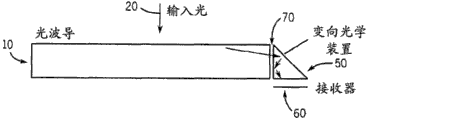
Edge gatherer or optical waveguide are used to light, especially the collection of sunshine and gathering.To this application, edge gatherer or optical waveguide are defined as a kind of optical device, and it receives light from top surface, and the energy of being assembled are transmitted the edge of this equipment.Fig. 1 a rough schematic of xsect of optical waveguide 10 that draws.Fig. 1 b is that the 3D of same optical waveguide 10 represents.
In actual applications, the type of these optical waveguides 10 generally is United States Patent (USP) 7,664, the type of describing in 350 and 7,662,549.The other types of optical waveguide comprise fluorescent solar collector or dye fluorescence solar collector.The draw optical system of last type of Fig. 1 c.Input light 20 drops on a plurality of accumulation units 40 of crossing over light hole, and this waveguide 10 is collected the light assembled and it is sent to the edge 30 of waveguide 10 from all unit.
Summary of the invention
Yet, if 30 have a partial cover optical devices 50(to see Fig. 2 and 3a at the edge), make this light 20 by good mode break-in, many advantages are arranged.In Fig. 2, light 20 is sent to the edge 30 of waveguide 10 and is spent the receiver of placing to the bottom that is parallel to waveguide 10 60 by break-in about 90.The present invention of the clear expression of this paper describes various distinct methods, is used for these second level break-in optical devices 50 of design.The present invention helps to make more useful optical waveguide 10.To the key business criterion of this optical waveguide lens system, comprise degree and the manufacturability of compactedness, efficient, gathering.The different methods that is used for break-in influences these criterions by different way.
The application that should also be noted that this optical waveguide 10 or equipment is various.Luminous energy can be sent to various different receivers.Fig. 3 a comprises more poly collection or diffuse optical device to draw some examples of receiver 60 of 3d, and such as lens, compound parabolic collection optic device, photovoltaic cell or heat exchanger, they are more detailed description hereinafter.
Description of drawings
Fig. 1 a cross-sectional view of concept formula optical waveguide that draws; Fig. 1 b 3-D view of concept formula optical waveguide that draws; And Fig. 1 c draws and is used in optical waveguide in the solar energy collecting;
Fig. 2 embodiment of this optical system that draws;
The draw embodiment of lens receiver of Fig. 3 a; The draw embodiment of CPC receiver of Fig. 3 b; The draw embodiment of photovoltaic cell receiver of Fig. 3 c; And the draw embodiment of heat exchanger receiver of Fig. 3 d;
Fig. 4 a another embodiment of this optical system that draws; Fig. 4 b another embodiment of this optical system that draws; Fig. 4 c draws and has a plurality of optical systems adjacent one another are of break-in optical devices; Fig. 4 d draws does not have a plurality of optical systems adjacent one another are of break-in optical devices;
Fig. 5 a break-in optical devices that draw are integrated into embodiment in the waveguide; The embodiment that the break-in optical devices separate with waveguide and Fig. 5 b draws;
Fig. 6 a-b draw optical system around central shaft by the embodiment of mirror-polishing;
Fig. 7 a-c embodiment of the degree that the break-in optical devices revise to assemble that draws;
Fig. 8 a draws and adopts the break-in optical devices of total internal reflection; And the break-in optical devices that Fig. 8 b draws and adopts part to reflect;
Fig. 9 draws and adopts the break-in optical devices of reflection;
Figure 10 a draws and comprises parabolical break-in optical devices; Figure 10 b draws and comprises the parabolical break-in optical devices with part refraction; Figure 10 c draws and comprises the parabolical break-in optical devices with part reflecting material; And Figure 10 d draws and comprises the break-in optical devices of para-curve and flat facet;
The draw embodiment of the break-in optical devices of showing that TIR leaks of Figure 11 a; Draw another embodiment of the break-in optical devices of showing that TIR leaks of Figure 11 b; And draw another embodiment of the break-in optical devices of showing that TIR leaks of Figure 11 c;
Figure 12 a draws the embodiment of the break-in of air optical devices between break-in optical devices and receiver; And Figure 12 b draws the embodiment of the break-in of clad material optical devices is arranged between break-in optical devices and receiver;
Figure 13 a embodiment of optical system that draws; Figure 13 b embodiment of optical system of inclination angle waveguide that draws; And Figure 13 c draws the embodiment of the break-in of clad material optical devices is arranged between break-in optical devices and receiver;
The draw various different embodiment of light pipe break-in optical devices of Figure 14 a-c;
Figure 15 a draws the embodiment of the break-in of clad material optical devices between break-in optical devices and receiver; And Figure 15 b draws the embodiment of the break-in of clad material and glass optical devices is arranged between break-in optical devices and receiver;
Figure 16 a-e various different embodiment of optical system that draw;
The draw optical system of line symmetry of Figure 17 a; Figure 17 b axisymmetric optical system of drawing; And Figure 17 c-f draws the rotational symmetry optical system and the various different embodiment of the break-in optical devices that are associated; With
Figure 18 draws and being configured for the embodiment of the optical system that illumination uses.
Embodiment
In preferred embodiment shown in Fig. 4 a, come wide the causing perpendicular to collecting the plane of self-waveguide 10 to propagate.Break-in optical devices 50 make this light 20 break-ins, arrive receiver 60, in order to change the propagation angle of the light cone of light 20.
In a preferred embodiment, optical waveguide 10 makes light 20 break-ins, becomes the angle of propagating in waveguide 10 perpendicular to it substantially, shown in Fig. 4 b.Place on the plane that makes receiver 60 can be parallel to collection like this, as Fig. 4 c.Optical waveguide 10 does not have therewith relevant break-in optical devices if Fig. 4 d draws, and how waveguide 10 is interfered mutually with receiver 60." optical devices layer " (break-in optical devices 50) and " receiver layer " (receiver 60) thereby form the flat plate section of level, they are can be easily assembled and be paired together.This is two-layer can to form firm and durable laminated construction.Connection between the receiver 60, for example, electric interconnected between the photovoltaic cell receiver can be finished easilier.Along with receiver 60(as, photovoltaic cell) temperature rise, have receiver layer separately can realize that more effective hot transmission leaves the tool back plane heating radiator.
Below the particular problem that solves with break-in optical devices 50 of each section general introduction, and some method for optimizing that address this problem.
1. as the diverter of same or separate section
Break-in optical devices 50 can be configured to have with waveguide optical device 10 feature of identical fabrication portion, shown in Fig. 5 a.In another embodiment, it also can be divided portion, shown in Fig. 5 b.
Make by same section, to the advantage of waveguide 10 be-less manufacturing step, do not aim at and owing to do not have the potential more high-level efficiency of loss between the interface requiring between the part.
Separate section by waveguide 10 and break-in optical devices 60 parts is made, and can help to keep or strengthen the aggregation extent of light.Can work as total internal reflection (TIR) surface in interface 70, thereby light 20 is included in the waveguide 10.
2. mirror image
Fig. 6 a draw optical waveguide 10 and break-in optical devices 50 as discussed earlier have the collection area of the input light of pointing out 20 and the height of optic components.
In Fig. 6 b, the combination of waveguide 10 optical devices, break-in optical devices 50 and receiver 60 centers on central shaft by mirror-polishing.Thereafter, receiver 60 can be configured to a continuous part (one contiguous part).Therefore the collection area that transmits light to single receiver 60 is doubled, the not change of simultaneously total structure height-thereby the compactness of this structure is the twice of given receiver 60 areas.
In addition, the waveguide of whole mirror-polishing and the combination of break-in can be made by a part, simplify thereby make to make.
3. assemble the second level
The second level that is caused by break-in optical devices 50 is assembled and is represented with C2, and is defined as the input area A2 of break-in optical devices 50, with the ratio of the output area A3 of break-in optical devices 50.The degree of last gathering is with C
FinalExpression, and be defined as A1/A3.
In Fig. 7 a, the degree that break-in optical devices 50 increase from the gathering of optical waveguide 10.C
FinalTherefore greater than C1.When clumping factor was key parameter, such as in the cost of reduction photovoltaic cell material area with the reduction solar panels, it can be favourable assembling from the second level of break-in optical devices 50.
In the embodiment of Fig. 7 b, the degree (C that break-in optical devices 50 reduce from the gathering of optical waveguide 10
Final<1).In the specific embodiment of Fig. 7 b, simple flat facet 80 is arranged to the horizontal bottom with respect to optical waveguide 10, or the edge gatherer, becomes suitable low-angle (shallow angle), and the gathering of minimizing can be provided.In Fig. 7 c, this embodiment provides other example.Even optical waveguide 10 is carried at a low price considerable aggregation extent altogether, but break-in optical devices 80 make last clumping factor be reduced to about 2x.This for example when needs reduce the solar cell material twice, can be favourable, and also have big continuous solar-electricity pool area, make total optical system highly compact all the time.
4. the limit of total internal reflection
Total internal reflection (TIR) can be used, so that reflection is used for the light 20 of break-in.It is better than reflectance coating, because it almost is loss-free, drops on energy above it and coating will absorb some.It is also more cheap, because it eliminates additional fabrication steps and the material cost of reflectance coating.
Yet total internal reflection is only to providing the light greater than the incident angle of critical angle to take place, and this critical angle is that the refractive index by these optical devices and material around forms.
In the embodiment of Fig. 8 a, the flat break-in optical devices 50 that are in the TIR limit are shown.The angle θ that forms between light 90 and the interface normal is just in time greater than critical angle.Situation-this light that the angle when light 90 of drawing Figure 14 a-c can take place during less than critical angle is refracted by break-in optical devices 50 surfaces, is not sent to receiver 60.Thus, require to adopt TIR, then the much additional second level is assembled and can be occurred, keep simultaneously on the efficient, restriction is set.
5. reflectance coating
In another embodiment, can adopt reflectance coating, so that the more gathered light that allows than the TIR limit.Fig. 9 such embodiment that draws.In this case, similar among incident angle and Fig. 8 b, there light 90 is lost in fact.And here, light 90 replaces and is reflexed to reverberator 60 downwards.Therefore reverberator 100 allows break-in optical devices 50 to have with respect to optical waveguide 10 more high dipping forms, and this form can strengthen second level gathering and not pass through interface loss light.Yet (, as section 4 description hereinafter, be that reverberator absorbs some energy that drop on above it to the sacrifice of efficient).
6. Wan Qu break-in optical devices
Such as the bending section of parabolic segment 110 among Figure 10 a, providing aspect the gathering of the second level, can be more effective than flat surface.Curve such as para-curve, is the collecting optics surface, thereby can get light cone and it is finished second level aggregation extent from optical waveguide 10, offers receiver 60.
Yet it is enough steep that this curve 110 can become, and makes the incident angle of light 90 above the critical angle of total internal reflection, shown in Figure 10 b.Two schemes are possible.The first, can apply reflectance coating 120 in the section of curve 110, not so can see that in the section of this curve 110 light spills, shown in Figure 10 c.The second, para-curve 110 can be blocked on the TIR limit, and by the terminal identical angle of this curve, flat facet 130 is used, and makes like this along these break-in optical devices and always obtains TIR.This feature is shown in Figure 10 d.
" 7.TIR leakage "
In another embodiment again, when optical waveguide 10 and break-in optical devices 50 during by mirror-polishing, light 140 can be allowed from a little leakage on break-in optical devices 50 surfaces, because it is by the break-in surface collection on opposite and be sent to receiver 60, shown in Figure 11 a.Can increase the accessible second level like this and assemble, because break-in optical devices 50 surfaces can be placed with steeper angle, thereby dwindle the area that receiver 60 requires.
In another embodiment, the cascade of facet 160 is possible, in order to utilize this effect, more those facets 160 near the basal surface location are more steep, shown in Figure 11 b.Each facet 160 can be placed with suitable angle, makes the light that is incident on it, the two maximization of the gathering on the given angle scope and efficient.In addition, the curved surface 170 that is similar to the facet 160 of cascade can be employed, to reach identical result, shown in the embodiment of Figure 11 c.These break-in optical devices 50 can also comprise multiple curve.Such as parabolic segment 170 and arc 180, shown in Figure 11 c.
8. the covering on the bottom
In another embodiment, if between the top of the bottom of optical devices 50 (base) and receiver 60, use air 190, will reflect and increase cone angle from the light 210 of break-in optical devices 50 outgoing so, shown in Figure 12 a.
Covering also will provide the advantage of efficient.Fresnel (Fresnel) reflects the interface of present different refractivity, and the difference of refractive index is more big, and loss is more big.Between optical devices and the receiver 160 air is arranged, will cause maximum Fresnel reflection loss.
Covering can also provide on the structure and reliability on advantage.It can encapsulate the sensitive material of necessary environment protection, such as photovoltaic cell.It can also be to the stress decoupling between optical devices and the receiver 160, the stress of the different rates generation of for example expanding under temperature raises.
9. inclination angle photoconduction
In the embodiment that changes, the direction of propagation of light cone in the waveguide 10 is not necessarily exactly perpendicular to input light, shown in Figure 13 a.In a kind of variation, waveguide 220 can be configured to level angled, shown in Figure 13 b.
The inclination angle form of waveguide 10 is favourable to break-in optical devices 50, remains in the TIR limit because it allows the bigger second level to assemble.Reason is, because light has the less angle that needs break-in.Figure 13 b shows that this advantage-light 90 can be reflected back through total internal reflection on such as angle bigger shown in Figure 13 a.
When Figure 13 c draws covering 200 combinations on inclination angle waveguide 220 and bottom, the variation of facet 230 angles of requirement.Leave the extreme light of focal spot area (focal area) 25 in order to tackle reflection, last facet 24(" facet 2 ") must be with the facet 23(" facet 1 " than the front) littler angle occurs, otherwise be reflected off the light 235 of focal spot area 25, will and upwards escape by facet 2 refractions.
10. break-in light pipe
Additional embodiments relates to the increase aspect ratio, assembles in order to win the bigger second level.Figure 14 a draws and utilizes crooked light pipe 260 to make light 265 break-ins.The aspect ratio of optical waveguide 10-break-in optical devices 260 is done significantly bigger.Figure 14 b identical light pipe that draws, but the curved surface by finishing (tailoring) break-in optical devices, the break-in optical devices 260 of perhaps managing characteristic type become taper shape, obtain the second level and assemble.Figure 14 c similar scheme of drawing, but with the flat facet of break-in optical devices 260, replace crooked section.
Yet previous break-in optical devices 260 keep the compactedness of optical waveguide really.Can see following trading off thus:
The non-tube side case of TIR obtains the highest compactedness and top efficiency, but is not the highest gathering
The non-tube side case of reverberator obtains the highest compactedness and the highest gathering, but is not the highest efficient
TIR tube side case obtains the highest gathering and top efficiency, but is not the highest compactedness
11. bottom glass
Another embodiment also increases aspect ratio slightly, in order to win bigger gathering.Figure 15 a design discussed-have break-in optical devices 50 of covering layer 200 that draw.How Figure 15 b can be placed on the optical material sheet of like glass 270 on the bottom of waveguide-break-in structure of optical means if drawing.Additional height makes because light 275 has longer propagation can have the bigger second level to assemble, and the angle of marginal ray also owing to this more long pass broadcast last focal spot area (focal area) dwindled.
Bottom glass 270 can also work with barrier environment as machinery, and protection receiver 60(is as, solar cell), avoid entering dust and the moisture in optics space, and the mechanical stress of avoiding being derived from heat and other expansions and contraction.
12. be used for the support optical devices of central break-in
Because whole wave guide-break-in structure of optical means, be designed to collect light 20 from top surface effectively, the light 20 that drops on (above these break-in optical devices) on the central area of this structure also is necessary for optimum efficiency and is collected.
Figure 16 a embodiment of complete waveguide 10-break-in optical devices 50 combination that draws comprises the support optical devices for central break-in.It is so designed, and makes the input light 20 on the whole front surface that drops on optical waveguide 10, is sent to receiver 60.
The draw close-up view of central direction-changing area of Figure 16 b.Light 280 from optical waveguide 10 is drawn, and the path that arrives receiver 60 comes into question in front.
Problem is how to make the light 20 from central direction-changing area 50 advance to receiver 60.Three kinds of schemes are possible, preferably combine.The first, the design of optical waveguide 10 each sections may be modified as the surface that adapts to different angle on the break-in optical devices 50.In Figure 16 c, there are bigger lens 290 and facet 300 features in the system that light 280 is propagated by it, to adapt to break-in optical devices surface 310 towards the contraction gradually of receiver 60.Therefore, light 280 is propagated the path of passing through, the path of light 20 among other embodiment of optical waveguide 10 systems of describing before being different from.
The second, feature can be placed in the crown member, with guiding light 280 suitable place to the break-in optical devices 50, makes it be sent to receiver 60 like this.In Figure 16 d, the tooth feature 320 on the bottom of crown member makes light 280 break-ins, so that intersects in it and the district of break-in surface optical device 310 directly over receiver 60.Do not have this tooth feature 320, light 280 can not be mapped to receiver 60, and efficient is restricted, and perhaps receiver 60 must be wideer, to adapt to light 280, makes to assemble to be restricted.
The 3rd, fully near the light at the center of optics system, be allowed to direction and pass unchangeably.They had been mapped to break-in optical devices surface at 310 o'clock, stood some refractions, but they consequently guarantee that they terminate on the receiver 60 fully near the center of optics system.
Top option two and three, formation-namely, pure TIR is used to require the non-reverberator of whole break-in optical devices 310 usefulness.Reflectance coating on the break-in optical devices 310 can stop the incident ray from central direction-changing area, and efficient is restricted.
Many elements that Figure 16 a-e combination was discussed in each section of preferred embodiment in the past:
According to section 1, to make for simplifying, break-in optical devices 310 are made as a part with optical waveguide 10.
According to section 2, optical waveguide 10-break-in optical devices 50 by mirror-polishing, increase the compactedness of collecting area and entire equipment around central shaft.
According to section 3, optical waveguide 10 obtains the second level assembles, and makes C
FinalC1, the receiver cost reduced thereby reduce receiver 60 areas.
According to section 4, break-in optical devices 310 adopt total internal reflection, in order to make maximizing efficiency.
According to section 6, break-in optical devices 310 adopt para-curve, assemble to increase the second level, are reaching TIR limit place thereafter, block this curve with the flat facet that is attached to it.(this para-curve can be approximate by the some flat facet of obtaining similar results.)
According to section 7, break-in optical devices 310 allow " TIR leakage "-some light to be allowed to break through critical angle and to be refracted to mirror surface, and there, they still are received device 60 and collect.Allow this break-in surface 310 that steeper angle is arranged like this, the further second level is assembled becomes possibility.
According to section 8, covering 200 is used between break-in optical devices and the receiver, to strengthen gathering, efficient, structural support and reliability.
According to section 9, optical waveguide 10 is that the inclination angle waveguide-namely, waveguide 10 is not fully perpendicular to input light 20.Allow these break-in optical devices 310 to have like this and increase the steeper angle that assemble the obtainable second level.
According to section 12, support optical devices 290,300,320, be built in the optical waveguide 10 in the central direction-changing area of break-in optical devices 310 tops.These support optical devices to guarantee to be incident on the light on the central area, are sent to receiver 60 by break-in optical devices 310, make efficient and assemble maximization.As showing in the above, break-in optical devices 50 can be constituted by parabolic surface, oval surface, hyperbolic surface, arc, flat reflecting surface, the reflecting surface of repairing shape, total internal reflection surface, compound any of parabolic concentrator optical devices, light pipe and refractive component.
Each section described the mode of the various different embodiment of design break-in optical devices 50 before.Two kinds of other embodiments of break-in optical devices 50 are described below.All in the element application of describing before in following two embodiments.
Line symmetry optical devices and the contrast of rotational symmetry optical devices
Because xsect is depended in this design, so this optics can perhaps be provided by the fashion of extrusion of rotation shown in Figure 17 b by straight line fashion of extrusion shown in Figure 17 a.All elements of describing among the application are applicable to one of these two kinds extruding.
Yet, by the rotational symmetry optical devices of rotation extruding, in the face of extra challenge.Figure 17 c draws familiar situation-from the light 20 of optical waveguide 320 by break-in, downwards towards central receiver 60.But, press the rotation extruding, light 20 must be aimed at fully with the radius that coils, in order to be mapped to by (noting sharp any of rotating extruding of pointing to of break-in optical devices 330 downwards) on the break-in optical devices 330 that are designed for break-in.In Figure 17 d, off-centered slightly light 340 is not mapped to break-in optical devices 330 and does not arrive receiver 60.
In Figure 17 e, this is to be modified by the point that makes the turning axle displacement leave break-in optical devices 330.What thus, light 340 was faced is not to put but wall 350.Turning axle leaves the distance of the point 360 of optical devices, can be conditioned, so that the light 20 of all waveguides substantially is hunted down, makes maximizing efficiency.Weak point is to compare with the straight line extruding of identical cross-section design, a little less than the second level is assembled.
Figure 17 f embodiment of the another kind of scheme that addresses this problem that draws.Break-in optical devices point 360 is taken as turning axle and treats.But direction-changing area 50 has the vertical slit 380 that is cut open by the periodic intervals around this.These slits 380 can be filled by air or low-refraction clad material, and perhaps the wall 50 of direction-changing area can cover with reverberator.Eccentric light 340 will be mapped to being reflected back towards the center in the lump of wall 380.In once or after the reflection for several times of this " guided wave wall ", light 340 will be last and the break-in surface interaction of break-in optical devices 370, and by break-in, arrive receiver 60 downwards.This scheme can remain in the straight line extruding of identical cross-section the obtainable second level and assemble.If do not use reflectance coating, that is, total internal reflection is unique mechanism, and so this scheme also makes maximizing efficiency.
The opposite optical path that is used for light diffusion or illumination
In another embodiment again, the optical devices of describing among the application are to collect and assemble for light so far.Yet opposite optical system is the effective diffusing globe of light.
In Figure 18, light 400 enters this equipment from light source 290, in light source 290 theres, up to the present all is the central area on the receiver 60-basal plane.Light 400 is by break-in, enters optical waveguide 10 through break-in optical devices 50, and this optical waveguide 10 accepts the light of horizontal transmission substantially, and it is diffused into substantially output light 410 perpendicular to waveguide 10 surfaces.The top surface of waveguide 10 can be regulated with lens or other optical elements, so that by any angular range emission light.Therefore, this equipment is highly compact and effective diffusing globe.Application comprises, but is not limited to: the headlight of LED optical devices, light fixture, pointolite and automobile and taillight.
The description of the front of the embodiment of the invention provides for the purpose of illustration and description.Do not attempt to be exhaustive or to limit the invention to disclosed accurate form, the instruction above using for reference perhaps can be by requirement of using on the spot of the present invention, and modifications and variations are possible.Embodiment is selected and describes to explain principle of the present invention, and its practical application makes those skilled in the art, can by the concrete purposes that is suitable for expecting, utilize the present invention in various different embodiment and with various modification.
Claims (13)
1. optics lens system comprises:
Optical waveguide is used for collecting and assembles input light,
Receiver is used for receiving the light of being assembled,
The break-in optical devices are used for making the light redirection from optical waveguide to arrive this receiver.
2. according to the optics lens system of definition in the claim 1, these break-in optical devices integral part that is these optical waveguides wherein.
3. according to the optics lens system of definition in the claim 1, wherein these break-in optical devices are the separate parts from this optical waveguide.
4. according to the optics lens system of definition in the claim 1, wherein the degree of the gathering that is provided by optical waveguide is provided these break-in optical devices.
5. according to the optics lens system of definition in the claim 1, wherein these break-in optical devices are selected from the group that is made of parabolic surface, oval surface, hyperbolic surface, arc, flat reflecting surface, the reflecting surface of repairing shape, total internal reflection surface, compound parabolic concentrator optical devices, light pipe and refractive component.
6. according to the optics lens system of definition in the claim 1, wherein this optical waveguide and break-in optical devices,, are made from the receiver combination of these two systems and form a continuous receiver to form at least two systems by mirror-polishing around central shaft at least.
7. according to the optics lens system of definition in the claim 6, these break-in optical devices wherein allow some anaclasis from optical waveguide to these mirror image break-in optical devices, by this mirror image break-in optical devices transmission, are used for being collected by receiver.
8. according to the optics lens system that defines in the claim 1, wherein this optical waveguide contains optical element, input light in the district on these optical element guiding receivers towards the exterior face of these break-in optical devices, is used for being transferred to receiver by these break-in optical devices.
9. according to the optics lens system of definition in the claim 1, wherein this optical waveguide and these break-in optical devices,, are made from the receiver combination of these two systems and form a continuous receiver to form at least two systems by mirror-polishing around central shaft at least.
10. according to the optics lens system of definition in the claim 1, wherein this optics lens system is axisymmetric around turning axle.
11. according to the optics lens system of definition in the claim 10, wherein the marginating compartment of this turning axle and these break-in optical devices is opened, thereby guarantees to be transferred to receiver from optical waveguide from axle light.
12. according to the optics lens system of definition in the claim 10, wherein these break-in optical devices contain vertical air slots, low-index material or reflecting material, thereby guarantee to be reflected off vertical slit to receiver from optical waveguide from axle light.
13. an optical lighting system comprises:
Light source is used for providing input light,
Optical waveguide is used for the input light that diffusion is used for illumination,
The break-in optical devices are used for making the light redirection from receiver to arrive this optical waveguide.
Applications Claiming Priority (5)
| Application Number | Priority Date | Filing Date | Title |
|---|---|---|---|
| US40777210P | 2010-10-28 | 2010-10-28 | |
| US61/407,772 | 2010-10-28 | ||
| US12/939,348 | 2010-11-04 | ||
| US12/939,348 US8412010B2 (en) | 2007-09-10 | 2010-11-04 | Compact optics for concentration and illumination systems |
| PCT/US2011/057876 WO2012058304A2 (en) | 2010-10-28 | 2011-10-26 | Redirecting optics for concentration and illumination systems |
Publications (1)
| Publication Number | Publication Date |
|---|---|
| CN103238091A true CN103238091A (en) | 2013-08-07 |
Family
ID=45994720
Family Applications (1)
| Application Number | Title | Priority Date | Filing Date |
|---|---|---|---|
| CN2011800580891A Pending CN103238091A (en) | 2010-10-28 | 2011-10-26 | Redirecting optics for concentration and illumination systems |
Country Status (8)
| Country | Link |
|---|---|
| US (2) | US8705914B2 (en) |
| EP (1) | EP2633349A4 (en) |
| JP (1) | JP5944398B2 (en) |
| KR (1) | KR20130130707A (en) |
| CN (1) | CN103238091A (en) |
| AU (1) | AU2011319939A1 (en) |
| CA (1) | CA2815671C (en) |
| WO (1) | WO2012058304A2 (en) |
Families Citing this family (18)
| Publication number | Priority date | Publication date | Assignee | Title |
|---|---|---|---|---|
| EP2430741A4 (en) * | 2009-05-14 | 2017-06-21 | Sunboost Ltd. | Light collection system and method |
| TWI538239B (en) * | 2011-02-14 | 2016-06-11 | Light collection device and its light collection method | |
| EP2654317B1 (en) * | 2012-04-17 | 2014-06-18 | Siemens Aktiengesellschaft | Input/output component with display element |
| JP2015216138A (en) * | 2012-09-10 | 2015-12-03 | シャープ株式会社 | Solar cell module and photovoltaic power generation device |
| CN104903150B (en) | 2012-12-27 | 2018-08-07 | 金泰克斯公司 | Lighting system |
| US9714756B2 (en) | 2013-03-15 | 2017-07-25 | Morgan Solar Inc. | Illumination device |
| US9595627B2 (en) | 2013-03-15 | 2017-03-14 | John Paul Morgan | Photovoltaic panel |
| EP2971950B1 (en) | 2013-03-15 | 2021-05-19 | Morgan Solar Inc. | Light panel, optical assembly with improved interface and light panel with improved manufacturing tolerances |
| US9960303B2 (en) | 2013-03-15 | 2018-05-01 | Morgan Solar Inc. | Sunlight concentrating and harvesting device |
| US9985156B2 (en) | 2013-11-01 | 2018-05-29 | UNIVERSITé LAVAL | Optical concentrator/diffuser using graded index waveguide |
| JP2015099336A (en) * | 2013-11-20 | 2015-05-28 | 株式会社東芝 | Optical element and optical device |
| JP6461956B2 (en) * | 2013-12-23 | 2019-01-30 | ノバルティス アーゲー | Power supply for intraocular lens adjustment |
| TWI552516B (en) * | 2015-01-29 | 2016-10-01 | 國立交通大學 | Sunlight manipulating device |
| US10473904B2 (en) * | 2015-01-29 | 2019-11-12 | National Chiao Tung University | Sunlight modulation device with divergent reflection of converged sunlight for solar energy utilization |
| CN109891286A (en) | 2016-11-03 | 2019-06-14 | 巴斯夫欧洲公司 | Daylight illuminating system |
| TWI816767B (en) * | 2018-03-22 | 2023-10-01 | 日商日東電工股份有限公司 | Optical components and manufacturing methods |
| US11500206B2 (en) * | 2018-04-02 | 2022-11-15 | Magic Leap, Inc. | Waveguides with integrated optical elements and methods of making the same |
| ES2962433T3 (en) | 2018-09-23 | 2024-03-19 | Lmpg Inc | Luminary |
Citations (4)
| Publication number | Priority date | Publication date | Assignee | Title |
|---|---|---|---|---|
| US5357592A (en) * | 1993-08-17 | 1994-10-18 | Martin Marietta Corporation | Optical energy concentrator/reflector |
| US5521725A (en) * | 1993-11-05 | 1996-05-28 | Alliedsignal Inc. | Illumination system employing an array of microprisms |
| CN1453525A (en) * | 2002-04-27 | 2003-11-05 | 汤浩泉 | Waveguide-imitating solar energy acceptor |
| CN101809377A (en) * | 2007-09-10 | 2010-08-18 | 榕树能量公司 | Compact optics for concentration, aggregation and illumination of light energy |
Family Cites Families (164)
| Publication number | Priority date | Publication date | Assignee | Title |
|---|---|---|---|---|
| US705778A (en) | 1901-11-07 | 1902-07-29 | William Leggett Mccabe | Portable conveyer. |
| US3780722A (en) | 1972-04-26 | 1973-12-25 | Us Navy | Fiber optical solar collector |
| US4029519A (en) | 1976-03-19 | 1977-06-14 | The United States Of America As Represented By The United States Energy Research And Development Administration | Solar collector having a solid transmission medium |
| US4357486A (en) | 1978-03-16 | 1982-11-02 | Atlantic Richfield Company | Luminescent solar collector |
| US4199376A (en) * | 1978-11-06 | 1980-04-22 | Atlantic Richfield Company | Luminescent solar collector |
| US4337759A (en) * | 1979-10-10 | 1982-07-06 | John M. Popovich | Radiant energy concentration by optical total internal reflection |
| US4411490A (en) * | 1980-08-18 | 1983-10-25 | Maurice Daniel | Apparatus for collecting, distributing and utilizing solar radiation |
| US4344417A (en) | 1980-10-21 | 1982-08-17 | Jan Malecek | Solar energy collector |
| JPS5792874A (en) * | 1980-11-29 | 1982-06-09 | Toshiba Corp | Manufacture of multi-layer reflection preventing film for solar battery |
| US4379944A (en) | 1981-02-05 | 1983-04-12 | Varian Associates, Inc. | Grooved solar cell for deployment at set angle |
| US4863224A (en) | 1981-10-06 | 1989-09-05 | Afian Viktor V | Solar concentrator and manufacturing method therefor |
| US4505264A (en) | 1983-12-27 | 1985-03-19 | Universite Laval | Electromagnetic wave concentrator |
| JPS61163302A (en) * | 1985-01-14 | 1986-07-24 | Nippon Kokan Kk <Nkk> | Flat condenser |
| US5353075A (en) | 1988-08-17 | 1994-10-04 | In Focus Systems, Inc. | Convertible flat panel display system |
| US5828427A (en) | 1990-06-11 | 1998-10-27 | Reveo, Inc. | Computer-based image display systems having direct and projection modes of viewing |
| US5050946A (en) | 1990-09-27 | 1991-09-24 | Compaq Computer Corporation | Faceted light pipe |
| US5150960A (en) | 1991-12-06 | 1992-09-29 | General Motors Corporation | Rear license plate illumination |
| US5146354A (en) | 1991-05-07 | 1992-09-08 | Compaq Computer Corporation | LCD system with a backlight having a light source at a light pipe's edge and with the LCD enframed |
| JPH05142535A (en) | 1991-08-29 | 1993-06-11 | Meitaku Syst:Kk | Incident light supply device for edge light panel |
| US5542017A (en) | 1991-09-27 | 1996-07-30 | Koike; Yasuhiro | Light scattering light guide and applied optical apparatuses |
| JPH05127161A (en) | 1991-11-07 | 1993-05-25 | Rohm Co Ltd | Liquid crystal display device and its backlight |
| KR970008351B1 (en) | 1991-12-03 | 1997-05-23 | 샤프 가부시끼가이샤 | Liquid crystal display device |
| US5438484A (en) | 1991-12-06 | 1995-08-01 | Canon Kabushiki Kaisha | Surface lighting device and a display having such a lighting device |
| JP2692025B2 (en) | 1992-01-24 | 1997-12-17 | スタンレー電気株式会社 | Planar light emitter device |
| JP3025109B2 (en) | 1992-03-11 | 2000-03-27 | シャープ株式会社 | Light source and light source device |
| US5303322A (en) * | 1992-03-23 | 1994-04-12 | Nioptics Corporation | Tapered multilayer luminaire devices |
| US5528720A (en) | 1992-03-23 | 1996-06-18 | Minnesota Mining And Manufacturing Co. | Tapered multilayer luminaire devices |
| US5237641A (en) | 1992-03-23 | 1993-08-17 | Nioptics Corporation | Tapered multilayer luminaire devices |
| US6002829A (en) | 1992-03-23 | 1999-12-14 | Minnesota Mining And Manufacturing Company | Luminaire device |
| US5806955A (en) | 1992-04-16 | 1998-09-15 | Tir Technologies, Inc. | TIR lens for waveguide injection |
| JP2980776B2 (en) | 1992-06-04 | 1999-11-22 | 東ソー株式会社 | Backlight |
| JP3136200B2 (en) | 1992-07-22 | 2001-02-19 | 株式会社日立製作所 | Liquid crystal display |
| DE4227468C2 (en) | 1992-08-20 | 2002-01-17 | Teves Gmbh Alfred | Electrical switch unit, in particular for controlling air conditioning systems in motor vehicles |
| US5323477A (en) | 1992-08-24 | 1994-06-21 | Motorola, Inc. | Contact array imager with integral waveguide and electronics |
| JPH0695112A (en) | 1992-09-16 | 1994-04-08 | Hitachi Ltd | Prism plate and information display device formed by using this plate |
| US5339179A (en) | 1992-10-01 | 1994-08-16 | International Business Machines Corp. | Edge-lit transflective non-emissive display with angled interface means on both sides of light conducting panel |
| US5359691A (en) | 1992-10-08 | 1994-10-25 | Briteview Technologies | Backlighting system with a multi-reflection light injection system and using microprisms |
| US5499165A (en) | 1992-10-08 | 1996-03-12 | Holmes, Jr.; Lawrence | Transparent edge-lit lighting pane for displays |
| US5390276A (en) | 1992-10-08 | 1995-02-14 | Briteview Technologies | Backlighting assembly utilizing microprisms and especially suitable for use with a liquid crystal display |
| US5432876C1 (en) | 1992-10-19 | 2002-05-21 | Minnesota Mining & Mfg | Illumination devices and optical fibres for use therein |
| US5400224A (en) | 1993-01-08 | 1995-03-21 | Precision Lamp, Inc. | Lighting panel |
| KR0158247B1 (en) | 1993-01-19 | 1999-03-20 | 미따라이 하지메 | Light guide, illuminating device having the light guide and image reading device and information processing apparatus having the illuminating device |
| JPH06314069A (en) | 1993-03-03 | 1994-11-08 | Fujitsu Ltd | Illuminating device |
| JP3051591B2 (en) | 1993-03-05 | 2000-06-12 | 日本メジフィジックス株式会社 | Anti-adhesion agent for thallium-201 container |
| US6111622A (en) | 1993-03-12 | 2000-08-29 | Ois Optical Imaging Systems, Inc. | Day/night backlight for a liquid crystal display |
| AU6524694A (en) | 1993-03-29 | 1994-10-24 | Precision Lamp, Inc. | Flat thin uniform thickness large area light source |
| JP3781441B2 (en) | 1993-07-23 | 2006-05-31 | 康博 小池 | Light scattering light guide light source device and liquid crystal display device |
| US5485354A (en) | 1993-09-09 | 1996-01-16 | Precision Lamp, Inc. | Flat panel display lighting system |
| US5455882A (en) | 1993-09-29 | 1995-10-03 | Associated Universities, Inc. | Interactive optical panel |
| US6313892B2 (en) | 1993-10-05 | 2001-11-06 | Teledyne Lighting And Display Products, Inc. | Light source utilizing reflective cavity having sloped side surfaces |
| EP0722576B1 (en) | 1993-10-05 | 2001-08-01 | Tir Technologies, Inc. | Light source for backlighting |
| US5440197A (en) | 1993-10-05 | 1995-08-08 | Tir Technologies, Inc. | Backlighting apparatus for uniformly illuminating a display panel |
| US5396350A (en) | 1993-11-05 | 1995-03-07 | Alliedsignal Inc. | Backlighting apparatus employing an array of microprisms |
| US5555329A (en) | 1993-11-05 | 1996-09-10 | Alliesignal Inc. | Light directing optical structure |
| US5428468A (en) | 1993-11-05 | 1995-06-27 | Alliedsignal Inc. | Illumination system employing an array of microprisms |
| US6129439A (en) | 1993-11-05 | 2000-10-10 | Alliedsignal Inc. | Illumination system employing an array of multi-faceted microprisms |
| US5477239A (en) | 1993-11-12 | 1995-12-19 | Dell Usa, L.P. | Front lighting system for liquid crystal display |
| US5598281A (en) | 1993-11-19 | 1997-01-28 | Alliedsignal Inc. | Backlight assembly for improved illumination employing tapered optical elements |
| US5390085A (en) | 1993-11-19 | 1995-02-14 | Motorola, Inc. | Light diffuser for a liquid crystal display |
| US5479275A (en) | 1993-12-03 | 1995-12-26 | Ois Optical Imaging Systems, Inc. | Backlit liquid crystal display with integral collimating, refracting, and reflecting means which refracts and collimates light from a first light source and reflects light from a second light source |
| US5485291A (en) | 1994-02-22 | 1996-01-16 | Precision Lamp, Inc. | Uniformly thin, high efficiency large area lighting panel with two facet grooves that are spaced apart and have light source facing facets with smaller slopes than the facets facing away from the light source |
| US5982540A (en) | 1994-03-16 | 1999-11-09 | Enplas Corporation | Surface light source device with polarization function |
| CA2134902C (en) | 1994-04-07 | 2000-05-16 | Friedrich Bertignoll | Light diffusing apparatus |
| JPH07294745A (en) * | 1994-04-25 | 1995-11-10 | Fanuc Ltd | Back light panel |
| JP3538220B2 (en) | 1994-05-25 | 2004-06-14 | 株式会社エンプラス | Corner light supply type surface light source device |
| US5671994A (en) | 1994-06-08 | 1997-09-30 | Clio Technologies, Inc. | Flat and transparent front-lighting system using microprisms |
| US5692066A (en) | 1994-09-20 | 1997-11-25 | Neopath, Inc. | Method and apparatus for image plane modulation pattern recognition |
| US5506929A (en) | 1994-10-19 | 1996-04-09 | Clio Technologies, Inc. | Light expanding system for producing a linear or planar light beam from a point-like light source |
| WO1996017207A1 (en) | 1994-11-29 | 1996-06-06 | Precision Lamp, Inc. | Edge light for panel display |
| US5579134A (en) | 1994-11-30 | 1996-11-26 | Honeywell Inc. | Prismatic refracting optical array for liquid flat panel crystal display backlight |
| US5659643A (en) | 1995-01-23 | 1997-08-19 | Minnesota Mining And Manufacturing Company | Notched fiber array illumination device |
| JP3251452B2 (en) | 1995-01-31 | 2002-01-28 | シャープ株式会社 | Backlight device for liquid crystal display device |
| US5608837A (en) | 1995-05-15 | 1997-03-04 | Clio Technologies, Inc. | Transmissive type display and method capable of utilizing ambient light |
| US5621833A (en) | 1995-06-12 | 1997-04-15 | Lau; Ronnie C. | Superposition of two-dimensional arrays |
| US5631994A (en) | 1995-08-23 | 1997-05-20 | Minnesota Mining And Manufacturing Company | Structured surface light extraction overlay and illumination system |
| US5877874A (en) | 1995-08-24 | 1999-03-02 | Terrasun L.L.C. | Device for concentrating optical radiation |
| US6104454A (en) | 1995-11-22 | 2000-08-15 | Hitachi, Ltd | Liquid crystal display |
| US5710793A (en) | 1995-12-21 | 1998-01-20 | National Semiconductor Corporation | Error signal quantization method and hardware for mixed blind and decision directed equalization |
| US5905826A (en) | 1996-01-24 | 1999-05-18 | Minnesota Mining And Manufacturing Co. | Conspicuity marking system including light guide and retroreflective structure |
| US6072551A (en) | 1996-02-14 | 2000-06-06 | Physical Optics Corporation | Backlight apparatus for illuminating a display with controlled light output characteristics |
| US5838403A (en) | 1996-02-14 | 1998-11-17 | Physical Optics Corporation | Liquid crystal display system with internally reflecting waveguide for backlighting and non-Lambertian diffusing |
| DE19610816C2 (en) | 1996-03-19 | 1999-02-04 | Ctx Opto Electronics Corp | Backlight system for a scoreboard |
| US5926601A (en) | 1996-05-02 | 1999-07-20 | Briteview Technologies, Inc. | Stacked backlighting system using microprisms |
| AUPO053896A0 (en) * | 1996-06-17 | 1996-07-11 | Franklin, James Bruce | Improvements in natural lighting |
| JP3702537B2 (en) | 1996-06-21 | 2005-10-05 | カシオ計算機株式会社 | Light source device |
| US5914760A (en) | 1996-06-21 | 1999-06-22 | Casio Computer Co., Ltd. | Surface light source device and liquid crystal display device using the same |
| US6005343A (en) | 1996-08-30 | 1999-12-21 | Rakhimov; Alexander Tursunovich | High intensity lamp |
| US5870156A (en) | 1996-09-05 | 1999-02-09 | Northern Telecom Limited | Shadow mask for backlit LCD |
| US5854872A (en) | 1996-10-08 | 1998-12-29 | Clio Technologies, Inc. | Divergent angle rotator system and method for collimating light beams |
| JPH10221528A (en) | 1996-12-05 | 1998-08-21 | Toyota Motor Corp | Solar battery device |
| US6473554B1 (en) | 1996-12-12 | 2002-10-29 | Teledyne Lighting And Display Products, Inc. | Lighting apparatus having low profile |
| EP0863422B1 (en) | 1997-03-04 | 2006-10-04 | Matsushita Electric Industrial Co., Ltd. | Linear beam irradiator |
| US6007209A (en) | 1997-03-19 | 1999-12-28 | Teledyne Industries, Inc. | Light source for backlighting |
| US6123431A (en) | 1997-03-19 | 2000-09-26 | Sanyo Electric Co., Ltd | Backlight apparatus and light guide plate |
| EP0867747A3 (en) | 1997-03-25 | 1999-03-03 | Sony Corporation | Reflective display device |
| US6879354B1 (en) | 1997-03-28 | 2005-04-12 | Sharp Kabushiki Kaisha | Front-illuminating device and a reflection-type liquid crystal display using such a device |
| US6992733B1 (en) | 1997-04-11 | 2006-01-31 | Micron Technology, Inc. | Backlighting system for an LCD |
| JPH10298605A (en) | 1997-04-22 | 1998-11-10 | Nissan Motor Co Ltd | Production of magnetostrictive material |
| US6097549A (en) * | 1997-08-12 | 2000-08-01 | Breault Research Organization, Inc. | Bireflective lens element |
| US6164799A (en) | 1997-09-19 | 2000-12-26 | Decoma International Inc. | Optics for separation of high and low intensity light |
| US6021007A (en) | 1997-10-18 | 2000-02-01 | Murtha; R. Michael | Side-collecting lightguide |
| US6057505A (en) | 1997-11-21 | 2000-05-02 | Ortabasi; Ugur | Space concentrator for advanced solar cells |
| US6151089A (en) | 1998-01-20 | 2000-11-21 | Sony Corporation | Reflection type display with light waveguide with inclined and planar surface sections |
| US6497939B1 (en) | 1998-02-03 | 2002-12-24 | Nippon Zeon Co., Ltd. | Flat plate and light guide plate |
| JPH11259007A (en) | 1998-03-10 | 1999-09-24 | Sony Corp | Reflection type display device |
| US6134092A (en) | 1998-04-08 | 2000-10-17 | Teledyne Lighting And Display Products, Inc. | Illumination device for non-emissive displays |
| JP3119241B2 (en) | 1998-07-01 | 2000-12-18 | 日本電気株式会社 | Liquid crystal display |
| US6428198B1 (en) | 1998-07-07 | 2002-08-06 | Alliedsignal Inc. | Display system having a light source separate from a display device |
| US6234656B1 (en) | 1998-08-20 | 2001-05-22 | Physical Optics Corporation | Fiber optic luminaire |
| GB9905642D0 (en) | 1999-03-11 | 1999-05-05 | Imperial College | Light concentrator for PV cells |
| US6623132B2 (en) | 1999-08-11 | 2003-09-23 | North American Lighting, Inc. | Light coupler hingedly attached to a light guide for automotive lighting |
| JP2001127331A (en) | 1999-10-29 | 2001-05-11 | Sanyo Electric Co Ltd | Solar battery module |
| US6440769B2 (en) | 1999-11-26 | 2002-08-27 | The Trustees Of Princeton University | Photovoltaic device with optical concentrator and method of making the same |
| ES2157846B1 (en) * | 1999-12-02 | 2002-03-01 | Univ Madrid Politecnica | DEVICE WITH DISCONTINUOUS LENS WITH INTERNAL TOTAL REFLECTION AND ASPHERIC DIOPTRIC FOR CONCENTRATION OR COLIMATION OF RADIANT ENERGY. |
| US6930818B1 (en) | 2000-03-03 | 2005-08-16 | Sipix Imaging, Inc. | Electrophoretic display and novel process for its manufacture |
| US6347874B1 (en) | 2000-02-16 | 2002-02-19 | 3M Innovative Properties Company | Wedge light extractor with risers |
| US6639349B1 (en) | 2000-06-16 | 2003-10-28 | Rockwell Collins, Inc. | Dual-mode LCD backlight |
| JP3932407B2 (en) | 2000-07-03 | 2007-06-20 | ミネベア株式会社 | Surface lighting device |
| JP2002289900A (en) | 2001-03-23 | 2002-10-04 | Canon Inc | Concentrating solar cell module and concentrating photovoltaic power generation system |
| US6738051B2 (en) | 2001-04-06 | 2004-05-18 | 3M Innovative Properties Company | Frontlit illuminated touch panel |
| US6592234B2 (en) | 2001-04-06 | 2003-07-15 | 3M Innovative Properties Company | Frontlit display |
| KR100765138B1 (en) | 2001-04-09 | 2007-10-15 | 삼성전자주식회사 | Backlight assembly and liquid crystal display device using thereof |
| US6957904B2 (en) | 2001-07-30 | 2005-10-25 | 3M Innovative Properties Company | Illumination device utilizing displaced radiation patterns |
| US6576887B2 (en) | 2001-08-15 | 2003-06-10 | 3M Innovative Properties Company | Light guide for use with backlit display |
| KR100789138B1 (en) | 2001-09-05 | 2007-12-27 | 삼성전자주식회사 | Illumination device and reflection type liquid crystal display device using the same |
| US6966684B2 (en) | 2001-09-13 | 2005-11-22 | Gelcore, Llc | Optical wave guide |
| DE20200571U1 (en) | 2002-01-15 | 2002-04-11 | Fer Fahrzeugelektrik Gmbh | vehicle light |
| US6796700B2 (en) | 2002-02-02 | 2004-09-28 | Edward Robert Kraft | Flat panel luminaire with remote light source and hollow light pipe for back lit signage applications |
| US6986660B2 (en) | 2002-06-04 | 2006-01-17 | Zimmer Dental, Inc. | Retaining screw with rententive feature |
| JP3923867B2 (en) | 2002-07-26 | 2007-06-06 | 株式会社アドバンスト・ディスプレイ | Planar light source device and liquid crystal display device using the same |
| US6842571B2 (en) | 2002-09-05 | 2005-01-11 | Motorola, Inc. | Optical interconnect system with layered lightpipe |
| US7063449B2 (en) | 2002-11-21 | 2006-06-20 | Element Labs, Inc. | Light emitting diode (LED) picture element |
| JP3767544B2 (en) | 2002-11-25 | 2006-04-19 | セイコーエプソン株式会社 | Optical device, illumination device, and projector |
| JP3776082B2 (en) | 2002-12-19 | 2006-05-17 | シャープ株式会社 | Solar cell module |
| US6840636B1 (en) * | 2003-05-08 | 2005-01-11 | Carl R Colvin | Solar diffusion loss compensator and collimator |
| JP2007027150A (en) | 2003-06-23 | 2007-02-01 | Hitachi Chem Co Ltd | Concentrating photovoltaic power generation system |
| US6966661B2 (en) | 2003-09-16 | 2005-11-22 | Robert L. Read | Half-round total internal reflection magnifying prism |
| JP4262113B2 (en) | 2004-02-13 | 2009-05-13 | シチズン電子株式会社 | Backlight |
| WO2005103562A2 (en) | 2004-04-23 | 2005-11-03 | Light Prescriptions Innovators, Llc | Optical manifold for light-emitting diodes |
| MX2007007229A (en) | 2004-12-17 | 2007-08-22 | Universal Biosensors Pty Ltd | Electromagnetic radiation collector. |
| US20060174867A1 (en) | 2004-12-28 | 2006-08-10 | Applied Optical Materials | Nonimaging solar collector/concentrator |
| CA2597342A1 (en) | 2005-02-10 | 2006-08-17 | Instapower Ltd. | A lighting device |
| US20080047605A1 (en) * | 2005-07-28 | 2008-02-28 | Regents Of The University Of California | Multi-junction solar cells with a homogenizer system and coupled non-imaging light concentrator |
| JP2009529791A (en) * | 2006-03-08 | 2009-08-20 | ライト プレスクリプションズ イノベーターズ エルエルシー | Solar concentrator |
| US7992361B2 (en) | 2006-04-13 | 2011-08-09 | Sabic Innovative Plastics Ip B.V. | Polymer panels and methods of making the same |
| WO2008131561A1 (en) | 2007-05-01 | 2008-11-06 | Morgan Solar Inc. | Light-guide solar panel and method of fabrication thereof |
| US9040808B2 (en) | 2007-05-01 | 2015-05-26 | Morgan Solar Inc. | Light-guide solar panel and method of fabrication thereof |
| WO2008157621A2 (en) | 2007-06-18 | 2008-12-24 | E-Cube Technologies, Inc. | Methods and apparatuses for waveguiding luminescence generated in a scattering medium |
| US8412010B2 (en) * | 2007-09-10 | 2013-04-02 | Banyan Energy, Inc. | Compact optics for concentration and illumination systems |
| US7672549B2 (en) | 2007-09-10 | 2010-03-02 | Banyan Energy, Inc. | Solar energy concentrator |
| WO2009063416A2 (en) | 2007-11-13 | 2009-05-22 | Koninklijke Philips Electronics, N.V. | Thin and efficient collecting optics for solar system |
| US7878190B2 (en) | 2007-11-28 | 2011-02-01 | Walter T Charlton | Solar collection apparatus, solar collection arrays, and related methods |
| KR20090058612A (en) * | 2007-12-05 | 2009-06-10 | 선문대학교 산학협력단 | Optical panel having light diffusing waveguides for backlight |
| WO2009121180A1 (en) | 2008-04-02 | 2009-10-08 | Morgan Solar Inc. | Solar panel window |
| CN102027183A (en) | 2008-04-02 | 2011-04-20 | 摩根阳光公司 | Solar panel window |
| US20100051089A1 (en) * | 2008-09-02 | 2010-03-04 | Qualcomm Mems Technologies, Inc. | Light collection device with prismatic light turning features |
| EP2351107A1 (en) | 2008-09-04 | 2011-08-03 | Morgan Solar Inc. | Staggered light collectors for concentrator solar panels |
| BRPI0918865A2 (en) * | 2008-09-19 | 2017-03-21 | Univ California | system and method for solar energy capture and related manufacturing method |
| WO2010062532A2 (en) * | 2008-10-27 | 2010-06-03 | The Regents Of The University Of California | Light concentration apparatus, systems and methods |
| ES2364665B1 (en) * | 2008-11-12 | 2012-05-23 | Abengoa Solar New Technologies, S.A. | LIGHTING AND CONCENTRATION SYSTEM. |
| CA2658193A1 (en) | 2009-03-12 | 2010-09-12 | Morgan Solar Inc. | Stimulated emission luminescent light-guide solar concentrators |
| WO2010124028A2 (en) | 2009-04-21 | 2010-10-28 | Vasylyev Sergiy V | Light collection and illumination systems employing planar waveguide |
| WO2011114240A2 (en) | 2010-03-19 | 2011-09-22 | Morgan Solar Inc. | Solar-light concentration apparatus |
| US20130104984A1 (en) | 2010-06-11 | 2013-05-02 | Morgan Solar Inc. | Monolithic photovoltaic solar concentrator |
-
2011
- 2011-10-26 WO PCT/US2011/057876 patent/WO2012058304A2/en active Application Filing
- 2011-10-26 EP EP11837013.9A patent/EP2633349A4/en not_active Withdrawn
- 2011-10-26 CN CN2011800580891A patent/CN103238091A/en active Pending
- 2011-10-26 AU AU2011319939A patent/AU2011319939A1/en not_active Abandoned
- 2011-10-26 US US13/282,147 patent/US8705914B2/en not_active Expired - Fee Related
- 2011-10-26 KR KR1020137010535A patent/KR20130130707A/en not_active Application Discontinuation
- 2011-10-26 JP JP2013536777A patent/JP5944398B2/en not_active Expired - Fee Related
- 2011-10-26 CA CA2815671A patent/CA2815671C/en not_active Expired - Fee Related
-
2014
- 2014-03-31 US US14/230,989 patent/US9229144B2/en not_active Expired - Fee Related
Patent Citations (4)
| Publication number | Priority date | Publication date | Assignee | Title |
|---|---|---|---|---|
| US5357592A (en) * | 1993-08-17 | 1994-10-18 | Martin Marietta Corporation | Optical energy concentrator/reflector |
| US5521725A (en) * | 1993-11-05 | 1996-05-28 | Alliedsignal Inc. | Illumination system employing an array of microprisms |
| CN1453525A (en) * | 2002-04-27 | 2003-11-05 | 汤浩泉 | Waveguide-imitating solar energy acceptor |
| CN101809377A (en) * | 2007-09-10 | 2010-08-18 | 榕树能量公司 | Compact optics for concentration, aggregation and illumination of light energy |
Also Published As
| Publication number | Publication date |
|---|---|
| EP2633349A4 (en) | 2014-11-12 |
| WO2012058304A2 (en) | 2012-05-03 |
| CA2815671C (en) | 2016-12-13 |
| EP2633349A2 (en) | 2013-09-04 |
| US20120099325A1 (en) | 2012-04-26 |
| JP5944398B2 (en) | 2016-07-05 |
| JP2013543991A (en) | 2013-12-09 |
| AU2011319939A1 (en) | 2013-05-23 |
| AU2011319939A2 (en) | 2013-07-11 |
| US8705914B2 (en) | 2014-04-22 |
| KR20130130707A (en) | 2013-12-02 |
| US9229144B2 (en) | 2016-01-05 |
| WO2012058304A3 (en) | 2012-07-19 |
| WO2012058304A4 (en) | 2012-09-27 |
| CA2815671A1 (en) | 2012-05-03 |
| US20140268809A1 (en) | 2014-09-18 |
Similar Documents
| Publication | Publication Date | Title |
|---|---|---|
| CN103238091A (en) | Redirecting optics for concentration and illumination systems | |
| CN101809377B (en) | Compact optics for concentration, aggregation and illumination of light energy | |
| CA2816065C (en) | Compact optics for concentration and illumination systems | |
| CN102216695B (en) | System and method for solar energy capture and related method of manufacturing | |
| CN101375112A (en) | A hybrid primary optical component for optical concentrators | |
| CN102483483A (en) | Stepped light collection and concentration system, components thereof, and methods | |
| Vu et al. | Optical fiber daylighting system combined with LED lighting and CPV based on stepped thickness waveguide for indoor lighting | |
| AU2010246958B2 (en) | Light collection system and method | |
| Li et al. | An optimal design analysis of a novel parabolic trough lighting and thermal system | |
| AU2012223120B2 (en) | Compact optics for concentration, aggregation and illumination of light energy |
Legal Events
| Date | Code | Title | Description |
|---|---|---|---|
| C06 | Publication | ||
| PB01 | Publication | ||
| C10 | Entry into substantive examination | ||
| SE01 | Entry into force of request for substantive examination | ||
| WD01 | Invention patent application deemed withdrawn after publication |
Application publication date: 20130807 |
|
| WD01 | Invention patent application deemed withdrawn after publication |