CN1299248C - Active matrix type display and its checking method - Google Patents
Active matrix type display and its checking method Download PDFInfo
- Publication number
- CN1299248C CN1299248C CNB021185298A CN02118529A CN1299248C CN 1299248 C CN1299248 C CN 1299248C CN B021185298 A CNB021185298 A CN B021185298A CN 02118529 A CN02118529 A CN 02118529A CN 1299248 C CN1299248 C CN 1299248C
- Authority
- CN
- China
- Prior art keywords
- mentioned
- display element
- transistor
- additional capacitor
- transistor seconds
- Prior art date
- Legal status (The legal status is an assumption and is not a legal conclusion. Google has not performed a legal analysis and makes no representation as to the accuracy of the status listed.)
- Expired - Fee Related
Links
Images


Classifications
-
- G—PHYSICS
- G02—OPTICS
- G02F—OPTICAL DEVICES OR ARRANGEMENTS FOR THE CONTROL OF LIGHT BY MODIFICATION OF THE OPTICAL PROPERTIES OF THE MEDIA OF THE ELEMENTS INVOLVED THEREIN; NON-LINEAR OPTICS; FREQUENCY-CHANGING OF LIGHT; OPTICAL LOGIC ELEMENTS; OPTICAL ANALOGUE/DIGITAL CONVERTERS
- G02F1/00—Devices or arrangements for the control of the intensity, colour, phase, polarisation or direction of light arriving from an independent light source, e.g. switching, gating or modulating; Non-linear optics
- G02F1/01—Devices or arrangements for the control of the intensity, colour, phase, polarisation or direction of light arriving from an independent light source, e.g. switching, gating or modulating; Non-linear optics for the control of the intensity, phase, polarisation or colour
- G02F1/13—Devices or arrangements for the control of the intensity, colour, phase, polarisation or direction of light arriving from an independent light source, e.g. switching, gating or modulating; Non-linear optics for the control of the intensity, phase, polarisation or colour based on liquid crystals, e.g. single liquid crystal display cells
- G02F1/133—Constructional arrangements; Operation of liquid crystal cells; Circuit arrangements
- G02F1/136—Liquid crystal cells structurally associated with a semi-conducting layer or substrate, e.g. cells forming part of an integrated circuit
-
- G—PHYSICS
- G09—EDUCATION; CRYPTOGRAPHY; DISPLAY; ADVERTISING; SEALS
- G09G—ARRANGEMENTS OR CIRCUITS FOR CONTROL OF INDICATING DEVICES USING STATIC MEANS TO PRESENT VARIABLE INFORMATION
- G09G3/00—Control arrangements or circuits, of interest only in connection with visual indicators other than cathode-ray tubes
- G09G3/20—Control arrangements or circuits, of interest only in connection with visual indicators other than cathode-ray tubes for presentation of an assembly of a number of characters, e.g. a page, by composing the assembly by combination of individual elements arranged in a matrix no fixed position being assigned to or needed to be assigned to the individual characters or partial characters
- G09G3/22—Control arrangements or circuits, of interest only in connection with visual indicators other than cathode-ray tubes for presentation of an assembly of a number of characters, e.g. a page, by composing the assembly by combination of individual elements arranged in a matrix no fixed position being assigned to or needed to be assigned to the individual characters or partial characters using controlled light sources
- G09G3/30—Control arrangements or circuits, of interest only in connection with visual indicators other than cathode-ray tubes for presentation of an assembly of a number of characters, e.g. a page, by composing the assembly by combination of individual elements arranged in a matrix no fixed position being assigned to or needed to be assigned to the individual characters or partial characters using controlled light sources using electroluminescent panels
- G09G3/32—Control arrangements or circuits, of interest only in connection with visual indicators other than cathode-ray tubes for presentation of an assembly of a number of characters, e.g. a page, by composing the assembly by combination of individual elements arranged in a matrix no fixed position being assigned to or needed to be assigned to the individual characters or partial characters using controlled light sources using electroluminescent panels semiconductive, e.g. using light-emitting diodes [LED]
- G09G3/3208—Control arrangements or circuits, of interest only in connection with visual indicators other than cathode-ray tubes for presentation of an assembly of a number of characters, e.g. a page, by composing the assembly by combination of individual elements arranged in a matrix no fixed position being assigned to or needed to be assigned to the individual characters or partial characters using controlled light sources using electroluminescent panels semiconductive, e.g. using light-emitting diodes [LED] organic, e.g. using organic light-emitting diodes [OLED]
- G09G3/3225—Control arrangements or circuits, of interest only in connection with visual indicators other than cathode-ray tubes for presentation of an assembly of a number of characters, e.g. a page, by composing the assembly by combination of individual elements arranged in a matrix no fixed position being assigned to or needed to be assigned to the individual characters or partial characters using controlled light sources using electroluminescent panels semiconductive, e.g. using light-emitting diodes [LED] organic, e.g. using organic light-emitting diodes [OLED] using an active matrix
- G09G3/3233—Control arrangements or circuits, of interest only in connection with visual indicators other than cathode-ray tubes for presentation of an assembly of a number of characters, e.g. a page, by composing the assembly by combination of individual elements arranged in a matrix no fixed position being assigned to or needed to be assigned to the individual characters or partial characters using controlled light sources using electroluminescent panels semiconductive, e.g. using light-emitting diodes [LED] organic, e.g. using organic light-emitting diodes [OLED] using an active matrix with pixel circuitry controlling the current through the light-emitting element
-
- G—PHYSICS
- G09—EDUCATION; CRYPTOGRAPHY; DISPLAY; ADVERTISING; SEALS
- G09G—ARRANGEMENTS OR CIRCUITS FOR CONTROL OF INDICATING DEVICES USING STATIC MEANS TO PRESENT VARIABLE INFORMATION
- G09G2300/00—Aspects of the constitution of display devices
- G09G2300/04—Structural and physical details of display devices
- G09G2300/0421—Structural details of the set of electrodes
- G09G2300/0426—Layout of electrodes and connections
-
- G—PHYSICS
- G09—EDUCATION; CRYPTOGRAPHY; DISPLAY; ADVERTISING; SEALS
- G09G—ARRANGEMENTS OR CIRCUITS FOR CONTROL OF INDICATING DEVICES USING STATIC MEANS TO PRESENT VARIABLE INFORMATION
- G09G2300/00—Aspects of the constitution of display devices
- G09G2300/08—Active matrix structure, i.e. with use of active elements, inclusive of non-linear two terminal elements, in the pixels together with light emitting or modulating elements
- G09G2300/0809—Several active elements per pixel in active matrix panels
- G09G2300/0842—Several active elements per pixel in active matrix panels forming a memory circuit, e.g. a dynamic memory with one capacitor
- G09G2300/0852—Several active elements per pixel in active matrix panels forming a memory circuit, e.g. a dynamic memory with one capacitor being a dynamic memory with more than one capacitor
-
- G—PHYSICS
- G09—EDUCATION; CRYPTOGRAPHY; DISPLAY; ADVERTISING; SEALS
- G09G—ARRANGEMENTS OR CIRCUITS FOR CONTROL OF INDICATING DEVICES USING STATIC MEANS TO PRESENT VARIABLE INFORMATION
- G09G2320/00—Control of display operating conditions
- G09G2320/02—Improving the quality of display appearance
- G09G2320/0247—Flicker reduction other than flicker reduction circuits used for single beam cathode-ray tubes
-
- G—PHYSICS
- G09—EDUCATION; CRYPTOGRAPHY; DISPLAY; ADVERTISING; SEALS
- G09G—ARRANGEMENTS OR CIRCUITS FOR CONTROL OF INDICATING DEVICES USING STATIC MEANS TO PRESENT VARIABLE INFORMATION
- G09G2330/00—Aspects of power supply; Aspects of display protection and defect management
- G09G2330/08—Fault-tolerant or redundant circuits, or circuits in which repair of defects is prepared
-
- G—PHYSICS
- G09—EDUCATION; CRYPTOGRAPHY; DISPLAY; ADVERTISING; SEALS
- G09G—ARRANGEMENTS OR CIRCUITS FOR CONTROL OF INDICATING DEVICES USING STATIC MEANS TO PRESENT VARIABLE INFORMATION
- G09G3/00—Control arrangements or circuits, of interest only in connection with visual indicators other than cathode-ray tubes
- G09G3/006—Electronic inspection or testing of displays and display drivers, e.g. of LED or LCD displays
-
- G—PHYSICS
- G09—EDUCATION; CRYPTOGRAPHY; DISPLAY; ADVERTISING; SEALS
- G09G—ARRANGEMENTS OR CIRCUITS FOR CONTROL OF INDICATING DEVICES USING STATIC MEANS TO PRESENT VARIABLE INFORMATION
- G09G3/00—Control arrangements or circuits, of interest only in connection with visual indicators other than cathode-ray tubes
- G09G3/20—Control arrangements or circuits, of interest only in connection with visual indicators other than cathode-ray tubes for presentation of an assembly of a number of characters, e.g. a page, by composing the assembly by combination of individual elements arranged in a matrix no fixed position being assigned to or needed to be assigned to the individual characters or partial characters
Abstract
The present invention provides a display device in which a defect inspection that is in line with the actual display condition is easily conducted. When a first transistor for switching Tr1 is ON by a gate signal, a voltage signal in accordance with a data voltage signal input to the source terminal of the first transistor Tr1 is held in a storage capacitor. A second transistor Tr2 controls an amount of current supplied to an emissive element from a power source line PVdd in accordance with the voltage signal, and a charge is accumulated in an additional capacitor C2 in accordance with the amount of current thus controlled. Defect inspection corresponding to the actual display state can be performed by examining the charge accumulated in the additional capacitor C2.
Description
Technical field
The present invention relates to use the display device of the OEL (OrganicElectro Luminesence organic electroluminescent) etc. of TFT (Thin Film Transistor thin film transistor (TFT)).
Background technology
The active matrix type display of existing use TFT uses Fig. 5 to illustrate.Fig. 5 is the figure of the equivalent electrical circuit of per 1 pixel of expression.As shown in Figure 5, OEL is made of the first transistor Tr1 of switching usefulness and transistor seconds Tr2 and the maintenance capacitor C that element drives is used substantially as each pixel of the display device of display element.
The drain terminal of the first transistor Tr1 (D) is connected in the incoming line of data voltage signal (Vdata), and gate terminal (G) receives the input from the signal (Gate Sig) of outside.The source terminal (S) of this first transistor Tr1 is connected in terminal keeping capacitor C and the gate terminal (G) of transistor seconds Tr2.Keep the another terminal of capacitor C to be connected in the VSC line.
Apply supply voltage PVdd on the source terminal of transistor seconds Tr2 (S), drain terminal (D) is connected in the anode of OEL element.
Promptly, in the existing display device, for the first transistor Tr1, on its drain terminal (D), apply in the data voltage signal corresponding with the tone value of stipulating, go up the input signal at gate terminal (G), the first transistor Tr1 is a conducting state, keeps the electric charge corresponding with the magnitude of voltage of data voltage signal in keeping capacitor C.And, by the quantity of electric charge that keeps in this maintenance capacitor C, conducting state (resistance) between the source terminal (S) of control transistor seconds Tr2 and the drain terminal (D), the current value driving OEL element of the resistance value decision by supply voltage PVdd and this control.That is, go up the data voltage signal of input by the first transistor Tr1, the resistance value of control transistor seconds Tr2, and then control the current value that flows through OEL, OEL is luminous with the brightness of the tone of hope.
Such active matrix type display autoluminescence, frivolous can drive with low consumpting power, is expected to become display of future generation.But this display device is still in conceptual phase, at an easy rate, high precision and being used to expeditiously checks that the device of the defective of each pixel also proposes.
Current conduct has the display device of TFT in each pixel, known have an active matrix TFT LCD.Among this TFTLCD, LCD is controlled by the voltage that applies through each pixel TFT.Therefore, among the LCD, in the defect inspection in the TFT substrate, generally be the charge storage state of checking at keeping capacitor C, judge whether transistor is good.
But, control by above-mentioned existing current value under the situation of luminous tone of OEL, electric current between the source drain of the transistor seconds Tr2 that grid voltage is controlled by the voltage that keeps by the first transistor Tr1 and C for the brightness that makes each light-emitting component is arranged, need be used to the special device that uses this current value to check, can not check by existing test, be difficult under the actual displayed state, carry out at once defect inspection.
Summary of the invention
The present invention In view of the foregoing makes, and purpose provides a kind of display device that can easily carry out defect inspection under the show state of reality at once.
The present invention who is used to solve the problem of above-mentioned existing example is a kind of active matrix type display, it is characterized in that each pixel has display element; Switch the first transistor of usefulness; The maintenance electric capacity of the voltage signal that provides through this first transistor during the above-mentioned the first transistor conducting state is provided; Provide the transistor seconds of using from the element drives of the power of power lead to above-mentioned display element according to the above-mentioned voltage signal that keeps by above-mentioned maintenance electric capacity that applies on its grid; And a side electrode is connected between this transistor seconds and the above-mentioned display element, and the opposing party's electrode is connected in the current potential identical with the current potential of a side's of above-mentioned maintenance electric capacity electrode, accepts the additional capacitor of charge storage by the electric current that flows to above-mentioned display element from above-mentioned transistor seconds.
In a certain form of the present invention, above-mentioned additional capacitor is used to check the matrix array substrate that forms and constitute described pixel on this active matrix type display and substrate.Here, above-mentioned display element is with the brightness luminous light-emitting component corresponding with power is provided, and above-mentioned additional capacitor is provided by the quantity of power that provides to above-mentioned display element in the unit interval, controls the luminosity of above-mentioned display element.
For the present invention of the problem that solves above-mentioned existing example is a kind of inspection method of checking above-mentioned display device, it is characterized in that this active matrix type display has additional capacitor, the electrode of one side is connected between this transistor seconds and the above-mentioned display element, and the opposing party's electrode is connected in the identical current potential of current potential with a side's of above-mentioned maintenance electric capacity electrode; At this additional capacitor, storage and the corresponding electric charge of the magnitude of current that flows to above-mentioned display element from above-mentioned transistor seconds, under the stored state of this electric charge, above-mentioned transistor seconds is connected, by measuring charge stored on the above-mentioned additional capacitor, check the homogeneity of the magnitude of current that supplies to above-mentioned each display element from the mains side of supplying with above-mentioned display element.
Description of drawings
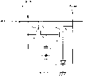
Fig. 1 is the circuit diagram of equivalent electrical circuit of 1 pixel in the active matrix type display of expression embodiments of the invention;
Fig. 2 is near the planimetric map of EL pixel of the active matrix type display of embodiments of the invention;
Fig. 3 is the diagrammatic sectional view along the A-A line of Fig. 2;
Fig. 4 is the diagrammatic sectional view along the B-B line of Fig. 2;
Fig. 5 is the circuit diagram of the equivalent electrical circuit of 1 pixel in the existing active matrix type display of expression.
Embodiment
Embodiments of the invention are described with reference to the accompanying drawings.Fig. 1 is the circuit diagram of equivalent electrical circuit of 1 pixel in the active matrix type display of expression embodiments of the invention.OEL is comprised the first transistor Tr1 that switches usefulness, transistor seconds Tr2 that element drives is used as shown in Figure 1 substantially, keeps capacitor C 1 and additional capacitor C2 as each pixel of the display device of the present embodiment of display element.And these pixels for example form a plurality of substrate shapes by matrix shape, constitute matrix array.For example, the envelope that regulation is set on the element formation face of this matrix array substrate is ended parts, makes display device.
The drain terminal of the first transistor Tr1 (D) is connected in the incoming line of data voltage signal (Vdata), and gate terminal (G) is accepted the input from the signal (Gate Sig) of outside.The source terminal (S) of this first transistor Tr1 is connected in terminal keeping capacitor C 1 and the gate terminal (G) of transistor seconds Tr2.Keep the another terminal of capacitor C 1 to be connected in VSC line 13.
Apply supply voltage PVdd on the source terminal of transistor seconds Tr2 (S), drain terminal (D) is connected in the anode of OEL element and the terminal of additional capacitor C2.Another terminal of additional capacitor C2 is connected in VSC line 13.
The operation of this circuit then is described.For the first transistor Tr1, on its drain terminal (D), apply in the data voltage signal corresponding with the tone value of stipulating, go up the input signal at gate terminal (G), Tr1 is made as conducting state with the first transistor, keeps the electric charge corresponding with the magnitude of voltage of data voltage signal in keeping capacitor C 1.
And, keep the quantity of electric charge that keeps in capacitor C 1 by this, conducting state (resistance) between the source terminal (S) of control transistor seconds Tr2 and the drain terminal (D), the current value driving OEL element of the resistance value decision by supply voltage PVdd and this control.At this moment, on the terminal of additional capacitor C2, also provide power, the storage electric charge corresponding on additional capacitor C2 with its power.
Near the EL pixel of Fig. 2 active matrix type display that to be each pixel represent with the equivalent electrical circuit of above-mentioned Fig. 1 planimetric map; Fig. 3 is the diagrammatic sectional view of expression along the A-A line; Fig. 4 is the diagrammatic sectional view of expression along the B-B line.As shown in Figure 2, at the data line 11 that extends on the column direction and gate line 12 area surrounded of extending on line direction is 1 pixel region, configuration the first transistor Tr1 in this zone, keeps capacitor C 1, transistor seconds Tr2, light-emitting zone R and additional capacitor C2.Here, keep island-shaped pattern 21 that capacitor C 1 comprises that the drain electrode of the first transistor Tr1 that forms from substrate is partly extended and through the island-shaped pattern of gate insulating film on VSC line 13 stacked on this island-shaped pattern 21.Form the line of assigning to source electrode portion from the drain portion of the first transistor Tr1 from this island-shaped pattern 21, be connected on the data line 11.Stacked gate insulating film and grid (G) on this line, in addition, the interlayer dielectric and first planarization insulating layer stack gradually.
The line 22 that partly extends from the drain electrode of transistor seconds Tr2 is connected in PVdd line 14, intersects through gate insulating film and grid, forms on substrate along the electrode 31 that constitutes additional capacitor C2.Here electrode 31 is connected in the island-shaped pattern (electrode that keeps capacitor C 1) on the VSC line 13.That is, be easy to form a electrode among the additional capacitor C2 by the pattern of line 22 being done some changes, another electrode 31 forms on same gate insulating film with the gate terminal of transistor seconds r2T.That is to say, with the VSC line 13 that keeps capacitor C 1 at same one deck, and form with VSC line 13.Therefore, do not need to add new manufacturing process in the formation of this additional capacitor C2.
In the present embodiment, the pair of electrodes that constitutes additional capacitor C2 forms near the light-emitting zone periphery, therefore forms the minimizing of the light-emitting zone of additional capacitor C2 generation, i.e. the reduction in aperture is also few, when considering that diffusion when luminous causes the light expansion, do not lose lightness.And, stack gradually interlayer dielectric, first planarization insulating layer on the VSC line 13 of another electrode 31 of the additional capacitor C2 that such light-emitting zone periphery forms and gate terminal (G) and maintenance capacitor C 1, stack gradually anode, hole transporting layer, luminescent layer, electron supplying layer on the additional capacitor C2, form negative electrode thereon.Part beyond these anodes, hole transporting layer, luminescent layer, the electron supplying layer is filled by second planarization insulating layer.
The active matrix type display of present embodiment has above structure, action as described below.
[danger is looked into]
When with each pixel of the active matrix type display that originally drove present embodiment in the same manner, additional capacitor C2 goes up storage and source terminal by the transistor seconds Tr2 that controlled by the voltage of the first transistor Tr1 and C1 maintenance to the corresponding electric charge of light-emitting component current amount flowing.Under the state of stored charge, connect transistor seconds Tr2 like this, the additional capacitor C2 that is determined at each pixel from power lead PVdd goes up charge stored.At this moment, the preferably tens of fF=several 10 of the capacitance C of additional capacitor C2
-15About F.
So, when additional capacitor C2 goes up charge stored amount and other pixels big-difference is arranged very, determine the current value difference that on the light-emitting component of this pixel, provides, can directly check the unusual of the current value that flows into to light-emitting component.
In addition, in this inspection, owing to measure the quantity of electric charge of additional capacitor C2, therefore can use the TFT of original LCD to check (be used to measure keep capacitor C electric charge) device of usefulness.
[mitigation of power-light characteristic]
When using the big light emitting element material of the variation that characteristic (performance number-light characteristic) sharply changes, brightness relative power value changes of luminescent substance, this element makes the magnitude of voltage control of TFT grid of the tone that obtains wishing by for example cold polymerization silicon TFT difficulty that becomes.At this moment, the TFT side requires to change significantly impedance, perhaps by using the different luminescent substance of rerum natura to deal with, but according to present embodiment, the time constant of the long-pending RC of the resistance value when capacitance C by this additional capacitor C2 and transistor seconds Tr2 connect, may command are applied to the effective value of voltage of light-emitting component and the magnitude of current that time per unit flows into light-emitting component.Thereby, do not change light emitting element material and can relax tone effectively yet, carry out brilliance control easily.At this moment, to be set at sec identical with driving frequency (if NTSC then is 60Hz, promptly 1/60 second) in the unit of the long-pending CR time constant of the capacitance C of additional capacitor C2 and the resistance value R of transistor seconds Tr2.
When on voltage signal line PVdd line, producing high frequency noise, during the fast luminescent substance of the response speed of use as OEL and fluorophor, change according to noise brightness, that is to say generation " flicker " (flick), but when the capacitance C of this additional capacitor C2 suitably sets, additional capacitor C2 can reduce the generation of flicker as the low-pass filter that removes this high frequency noise.At this moment, CR time constant below more than percent (about 10 of driving frequency preferably
-5Below second).
Even if being used among fluorescent display tube (VFD), LED, the inorganic EL etc., active matrix type display of the present invention also can obtain effect same.
The invention effect
According to the present invention, it is a kind of such active matrix type display, wherein each pixel of active matrix type display is during the first transistor that switches usefulness is on-state, the voltage signal that maintenance provides through this first transistor in keeping electric capacity, the voltage signal that keeps is applied on the grid of transistor seconds, transistor seconds provides the power from power lead corresponding with this voltage signal to display element, connect to come the feasible electric current that flows to display element by transistor seconds to accept the storage of electric charge additional capacitor, therefore after driving display element, measure charge stored amount on this additional capacitor, just the magnitude of current that provides through transistor seconds can be directly checked, defect inspection can be easily under the actual displayed state, carried out at once.
Claims (4)
1. an active matrix type display is characterized in that, each pixel has:
Display element; Switch the first transistor of usefulness; The maintenance electric capacity of the voltage signal that provides through this first transistor during the above-mentioned the first transistor conducting state is provided; According to the above-mentioned voltage signal that keeps by above-mentioned maintenance electric capacity that applies on its grid, provide the transistor seconds of using from the element drives of the power of power lead to above-mentioned display element; And a side electrode is connected between this transistor seconds and the above-mentioned display element, the opposing party's electrode is connected in the identical current potential of current potential with a side's of above-mentioned maintenance electric capacity electrode, by flowing to the electric current of above-mentioned display element, and accept the additional capacitor of charge storage from above-mentioned transistor seconds.
2. active matrix type display according to claim 1 is characterized in that:
Above-mentioned display element be according to from the said power electrical power supplied with the luminous electroluminescent cell of brightness;
Above-mentioned additional capacitor, the long-pending time constant of the resistance value when being controlled at the electric capacity of the electric power that supplies to above-mentioned display element in the unit interval and above-mentioned additional capacitor and above-mentioned transistor seconds conducting is controlled the luminosity of above-mentioned display element.
3. near the display pixel that the inspection method of an active matrix type display, this active matrix type display have many gate lines and many drain lines that intersect with this gate line, form each intersection point of this two line forms rectangular,
Each pixel has:
Display element; Switch the first transistor of usefulness; The maintenance electric capacity of the voltage signal that provides through this first transistor during the above-mentioned the first transistor conducting state is provided; According to the above-mentioned voltage signal that keeps by above-mentioned maintenance electric capacity that applies on its grid, provide the transistor seconds of using from the element drives of the power of power lead to above-mentioned display element;
It is characterized in that:
This active matrix type display has additional capacitor, and the electrode of one side is connected between this transistor seconds and the above-mentioned display element, and the opposing party's electrode is connected in the identical current potential of current potential with a side's of above-mentioned maintenance electric capacity electrode;
At this additional capacitor, storage and the corresponding electric charge of the magnitude of current that flows to above-mentioned display element from above-mentioned transistor seconds, under the stored state of this electric charge, above-mentioned transistor seconds is connected, by measuring charge stored on the above-mentioned additional capacitor, check the homogeneity of the magnitude of current that supplies to above-mentioned each display element from the mains side of supplying with above-mentioned display element.
4. the inspection method of active matrix type display according to claim 3 is characterized in that:
Above-mentioned display element be according to from the said power electrical power supplied with the luminous electroluminescent cell of brightness;
Above-mentioned additional capacitor is controlled at the long-pending time constant of the electric capacity of the electric power that supplies to above-mentioned display element in the unit interval and above-mentioned additional capacitor and the above-mentioned transistor seconds resistance value when leading, and controls the luminosity of above-mentioned display element.
Applications Claiming Priority (2)
| Application Number | Priority Date | Filing Date | Title |
|---|---|---|---|
| JP2001102303A JP2002297053A (en) | 2001-03-30 | 2001-03-30 | Active matrix type display device and inspection method therefor |
| JP102303/01 | 2001-03-30 |
Publications (2)
| Publication Number | Publication Date |
|---|---|
| CN1383116A CN1383116A (en) | 2002-12-04 |
| CN1299248C true CN1299248C (en) | 2007-02-07 |
Family
ID=18955519
Family Applications (1)
| Application Number | Title | Priority Date | Filing Date |
|---|---|---|---|
| CNB021185298A Expired - Fee Related CN1299248C (en) | 2001-03-30 | 2002-03-30 | Active matrix type display and its checking method |
Country Status (5)
| Country | Link |
|---|---|
| US (1) | US6768480B2 (en) |
| JP (1) | JP2002297053A (en) |
| KR (1) | KR100513184B1 (en) |
| CN (1) | CN1299248C (en) |
| TW (1) | TW589914B (en) |
Families Citing this family (30)
| Publication number | Priority date | Publication date | Assignee | Title |
|---|---|---|---|---|
| TW550528B (en) * | 2002-03-29 | 2003-09-01 | Chi Mei Optoelectronics Corp | Display device |
| JP3989763B2 (en) | 2002-04-15 | 2007-10-10 | 株式会社半導体エネルギー研究所 | Semiconductor display device |
| JP3527726B2 (en) | 2002-05-21 | 2004-05-17 | ウインテスト株式会社 | Inspection method and inspection device for active matrix substrate |
| JP4416456B2 (en) * | 2002-09-02 | 2010-02-17 | キヤノン株式会社 | Electroluminescence device |
| GB0229236D0 (en) * | 2002-12-12 | 2003-01-22 | Koninkl Philips Electronics Nv | AMLCD with integrated touch input |
| JP2004294457A (en) * | 2002-12-16 | 2004-10-21 | Agilent Technologies Japan Ltd | Active matrix display and its testing method |
| KR100490622B1 (en) * | 2003-01-21 | 2005-05-17 | 삼성에스디아이 주식회사 | Organic electroluminescent display and driving method and pixel circuit thereof |
| CN100437666C (en) * | 2003-05-12 | 2008-11-26 | 国际商业机器公司 | Active matrix panel inspection device, inspection method, and active matrix OLED panel manufacturing method |
| TWI229313B (en) * | 2003-09-12 | 2005-03-11 | Au Optronics Corp | Display pixel circuit and driving method thereof |
| JP3628014B1 (en) | 2003-09-19 | 2005-03-09 | ウインテスト株式会社 | Display device and inspection method and device for active matrix substrate used therefor |
| KR101002324B1 (en) * | 2003-12-22 | 2010-12-17 | 엘지디스플레이 주식회사 | Liquid Crystal Display Device and Driving Method Thereof |
| KR101054341B1 (en) * | 2004-04-30 | 2011-08-04 | 삼성전자주식회사 | Organic light emitting display device and manufacturing method thereof |
| TWI467531B (en) * | 2004-09-16 | 2015-01-01 | Semiconductor Energy Lab | Display device and driving method of the same |
| JP4186961B2 (en) * | 2004-10-26 | 2008-11-26 | セイコーエプソン株式会社 | Self-luminous device, driving method thereof, pixel circuit, and electronic device |
| JP2006154310A (en) * | 2004-11-29 | 2006-06-15 | Sanyo Electric Co Ltd | Display panel |
| CN100410989C (en) * | 2005-03-22 | 2008-08-13 | 友达光电股份有限公司 | Picture element array and its picture quality improving method |
| JP4923505B2 (en) | 2005-10-07 | 2012-04-25 | ソニー株式会社 | Pixel circuit and display device |
| JP2009092965A (en) * | 2007-10-10 | 2009-04-30 | Eastman Kodak Co | Failure detection method for display panel and display panel |
| JP4780159B2 (en) * | 2008-08-27 | 2011-09-28 | ソニー株式会社 | Display device and driving method thereof |
| US8884641B2 (en) | 2009-04-24 | 2014-11-11 | Arizona Board of Regents, a body corporated of the State of Arizona acting for and on behalf of Arizona State University | Methods and system for electrostatic discharge protection of thin-film transistor backplane arrays |
| WO2010123619A2 (en) | 2009-04-24 | 2010-10-28 | Arizona Board of Regents, a body corporate acting for and on behalf of Arizona State University | Methods and system for on-chip decoder for array test |
| WO2012056497A1 (en) * | 2010-10-28 | 2012-05-03 | パナソニック株式会社 | Method for inspecting active matrix substrate |
| JP5477359B2 (en) * | 2011-11-04 | 2014-04-23 | ソニー株式会社 | Display device |
| CN103488020A (en) * | 2013-08-09 | 2014-01-01 | 京东方科技集团股份有限公司 | Display panel, driving method of display panel and display device with display panel |
| CN103489404B (en) | 2013-09-30 | 2016-08-17 | 京东方科技集团股份有限公司 | Pixel cell, image element circuit and driving method thereof |
| KR20150042914A (en) * | 2013-10-14 | 2015-04-22 | 삼성디스플레이 주식회사 | Pixel and organic light emitting display device including the same |
| DE102015100859A1 (en) * | 2015-01-21 | 2016-07-21 | Osram Oled Gmbh | Method for operating a display device and display device |
| CN110189664A (en) * | 2019-05-15 | 2019-08-30 | 深圳市华星光电半导体显示技术有限公司 | The method that pixel array detects substrate and production method, detection pixel array substrate |
| CN110737126B (en) * | 2019-10-31 | 2022-03-29 | 厦门天马微电子有限公司 | Display panel and display device |
| CN112365846B (en) * | 2020-11-12 | 2021-10-08 | 深圳市华星光电半导体显示技术有限公司 | Pixel circuit and display device |
Citations (9)
| Publication number | Priority date | Publication date | Assignee | Title |
|---|---|---|---|---|
| US4532506A (en) * | 1981-10-30 | 1985-07-30 | Hitachi, Ltd. | Matrix display and driving method therefor |
| US4621260A (en) * | 1982-12-25 | 1986-11-04 | Tokyo Shibaura Denki Kabushiki Kaisha | Thin-film transistor circuit |
| JPH07199220A (en) * | 1993-12-28 | 1995-08-04 | Toshiba Corp | Array substrate |
| JPH10228009A (en) * | 1997-02-13 | 1998-08-25 | Toshiba Corp | Liquid crystal display device |
| US5903246A (en) * | 1997-04-04 | 1999-05-11 | Sarnoff Corporation | Circuit and method for driving an organic light emitting diode (O-LED) display |
| US5926158A (en) * | 1993-06-28 | 1999-07-20 | Sharp Kabushiki Kaisha | Image display apparatus |
| US5952789A (en) * | 1997-04-14 | 1999-09-14 | Sarnoff Corporation | Active matrix organic light emitting diode (amoled) display pixel structure and data load/illuminate circuit therefor |
| WO2000019401A1 (en) * | 1998-09-29 | 2000-04-06 | Sarnoff Corporation | Analog active matrix emissive display |
| JP2000347622A (en) * | 1999-06-07 | 2000-12-15 | Casio Comput Co Ltd | Display device and its driving method |
Family Cites Families (6)
| Publication number | Priority date | Publication date | Assignee | Title |
|---|---|---|---|---|
| US5302966A (en) * | 1992-06-02 | 1994-04-12 | David Sarnoff Research Center, Inc. | Active matrix electroluminescent display and method of operation |
| US5576726A (en) * | 1994-11-21 | 1996-11-19 | Motorola | Electro-luminescent display device driven by two opposite phase alternating voltages and method therefor |
| JPH11272235A (en) * | 1998-03-26 | 1999-10-08 | Sanyo Electric Co Ltd | Drive circuit of electroluminescent display device |
| US6392620B1 (en) * | 1998-11-06 | 2002-05-21 | Canon Kabushiki Kaisha | Display apparatus having a full-color display |
| JP3259774B2 (en) * | 1999-06-09 | 2002-02-25 | 日本電気株式会社 | Image display method and apparatus |
| JP2001281635A (en) * | 2000-03-30 | 2001-10-10 | Mitsubishi Electric Corp | Liquid crystal display device |
-
2001
- 2001-03-30 JP JP2001102303A patent/JP2002297053A/en active Pending
-
2002
- 2002-02-20 TW TW091102884A patent/TW589914B/en not_active IP Right Cessation
- 2002-03-21 KR KR10-2002-0015243A patent/KR100513184B1/en not_active IP Right Cessation
- 2002-03-27 US US10/109,146 patent/US6768480B2/en not_active Expired - Lifetime
- 2002-03-30 CN CNB021185298A patent/CN1299248C/en not_active Expired - Fee Related
Patent Citations (9)
| Publication number | Priority date | Publication date | Assignee | Title |
|---|---|---|---|---|
| US4532506A (en) * | 1981-10-30 | 1985-07-30 | Hitachi, Ltd. | Matrix display and driving method therefor |
| US4621260A (en) * | 1982-12-25 | 1986-11-04 | Tokyo Shibaura Denki Kabushiki Kaisha | Thin-film transistor circuit |
| US5926158A (en) * | 1993-06-28 | 1999-07-20 | Sharp Kabushiki Kaisha | Image display apparatus |
| JPH07199220A (en) * | 1993-12-28 | 1995-08-04 | Toshiba Corp | Array substrate |
| JPH10228009A (en) * | 1997-02-13 | 1998-08-25 | Toshiba Corp | Liquid crystal display device |
| US5903246A (en) * | 1997-04-04 | 1999-05-11 | Sarnoff Corporation | Circuit and method for driving an organic light emitting diode (O-LED) display |
| US5952789A (en) * | 1997-04-14 | 1999-09-14 | Sarnoff Corporation | Active matrix organic light emitting diode (amoled) display pixel structure and data load/illuminate circuit therefor |
| WO2000019401A1 (en) * | 1998-09-29 | 2000-04-06 | Sarnoff Corporation | Analog active matrix emissive display |
| JP2000347622A (en) * | 1999-06-07 | 2000-12-15 | Casio Comput Co Ltd | Display device and its driving method |
Also Published As
| Publication number | Publication date |
|---|---|
| KR100513184B1 (en) | 2005-09-08 |
| TW589914B (en) | 2004-06-01 |
| JP2002297053A (en) | 2002-10-09 |
| KR20020077070A (en) | 2002-10-11 |
| US6768480B2 (en) | 2004-07-27 |
| CN1383116A (en) | 2002-12-04 |
| US20020167472A1 (en) | 2002-11-14 |
Similar Documents
| Publication | Publication Date | Title |
|---|---|---|
| CN1299248C (en) | Active matrix type display and its checking method | |
| US7501658B2 (en) | Electro-luminescence device including a thin film transistor and method of fabricating an electro-luminescence device | |
| US6667791B2 (en) | Passive drive matrix display | |
| CN1897093A (en) | Display device and control method thereof | |
| CN1638542A (en) | Organic electroluminescent display device | |
| EP2190021A2 (en) | Organic electroluminescent display device and method and apparatus of manufacturing the same | |
| CN1455632A (en) | Organic electroluminescence device and its mfg. method | |
| CN1444200A (en) | Organic electroluminescent display whose power line and grid lind are parallel and its making method | |
| CN1356680A (en) | Method for darkening pixels | |
| CN1455631A (en) | Active matrix organic electroluminescence device and its mfg. method | |
| CN1555549A (en) | Drive circuit for light emitting elements | |
| CN1638548A (en) | Organic electroluminescent display device and method of fabricating the same | |
| JP2003243171A (en) | Organic electroluminescent display panel and its manufacturing method | |
| CN100401525C (en) | Organic electro-luminessence device and fabricating method thereof | |
| CN1622712A (en) | Organic electro luminescence display | |
| CN100590905C (en) | Organic light emitting diode device including brightness compensation plate | |
| US7497755B2 (en) | Apparatus for testing electroluminescent display | |
| CN1264131C (en) | Display device | |
| CN100353560C (en) | Organic light emitting display panel | |
| KR100855479B1 (en) | Active matrix flat panel display panel | |
| CN1636145A (en) | Method of healing of low-ohmic defects in a flat display | |
| JP2005331787A (en) | Display device | |
| JPS62189497A (en) | Driving of thin film el element |
Legal Events
| Date | Code | Title | Description |
|---|---|---|---|
| C06 | Publication | ||
| PB01 | Publication | ||
| C10 | Entry into substantive examination | ||
| SE01 | Entry into force of request for substantive examination | ||
| C14 | Grant of patent or utility model | ||
| GR01 | Patent grant | ||
| C17 | Cessation of patent right | ||
| CF01 | Termination of patent right due to non-payment of annual fee |
Granted publication date: 20070207 Termination date: 20100330 |