Background technology
As the memory storage that can carry out non-volatile data storage with low-power consumption, noticeable is MRAM (Magnetic Random Access Memory) equipment.MRAM equipment be to use a plurality of film magnets that on SIC (semiconductor integrated circuit), form to carry out non-volatile data storage and to each film magnet can random access memory storage.
The film magnet of particularly having delivered in recent years by utilizing magnetic tunnel-junction (MTJ:MagneticTunnel Junction) uses and the rapidly progressive information of performance of MRAM equipment as storage unit.
Figure 11 is the skeleton diagram of the structure of the storage unit (below, simply be called " mtj memory cell ") of expression with magnetic tunnel-junction portion.
Referring to Figure 11, mtj memory cell has resistance with the storage tunnel magnetoresistance element TMR that changes of data level be used to form the access element ATR in the path of the read current Is by tunnel magnetoresistance element TMR when data are read.Access element ATR is typically by field effect transistor and forms, so, below, also access element is called access transistor ATR.Access transistor ATR is connected between tunnel magnetoresistance element TMR and the fixed voltage (ground voltage Vss).
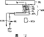
Figure 12 is the concept map that the explanation data of carrying out from mtj memory cell are read.
Referring to Figure 12, tunnel magnetoresistance element TMR comprise ferromagnetism body layer with fixing certain direction of magnetization (below, be called " fixed magnetization layer " simply) FL and being magnetized to and the ferromagnetism body layer of the outside corresponding direction of externally-applied magnetic field (below, be called " free magnetization layer " simply) VL.Between fixed magnetization layer FL and free magnetization layer VL, be provided with by the film formed tunnel barrier of insulator (tunnel film) TB.Free magnetization layer VL is magnetized to direction identical with fixed magnetization layer FL or the direction opposite with fixed magnetization layer FL according to the level of the storage data that write.Form magnetic tunnel-junction by fixed magnetization layer FL, tunnel barrier TB and free magnetization layer VL.
When data are read, access transistor ATR conducting with the activation of word line WL.Like this, just, can make read current Is flow through the current path of bit line BL~tunnel magnetoresistance element TMR~access transistor ATR~ground voltage Vss.
The resistance of tunnel magnetoresistance element TMR changes according to the relativeness of the direction of magnetization of fixed magnetization layer FL and free magnetization layer VL.Particularly, when the direction of magnetization identical (parallel) of the direction of magnetization of fixed magnetization layer FL and free magnetization layer VL, little during both direction of magnetization of the resistance ratio of tunnel magnetoresistance element opposite (antiparallel).
Therefore, if make free magnetization layer VL be magnetized to a certain direction in above-mentioned 2 kinds of directions according to the storage data, then the change in voltage that takes place owing to read current Is in tunnel magnetoresistance element TMR is just different with storing data level.Therefore, if after for example bit line BL being pre-charged to certain voltage, make read current Is flow through tunnel magnetoresistance element TMR, by detecting the voltage of bit line BL, just can read the storage data of mtj memory cell.
Figure 13 is the concept map of explanation to the data write activity of mtj memory cell.
Referring to Figure 13, write in data fashionable, the non-activation of word line WL, access transistor ATR ends.Under this state, be used for the data write current that free magnetization layer VL was magnetized to and write the corresponding direction of data flow through respectively and write digital line WDL and bit line BL.The direction of magnetization of free magnetization layer VL is by flowing through the data write current decision that writes digital line WDL and bit line BL respectively.
Figure 14 is that explanation is carried out the concept map of relation that data are write the direction of magnetization of fashionable data write current and tunnel magnetoresistance element to mtj memory cell.
Referring to Figure 14, transverse axis H (EA) is illustrated in the magnetic field that is added to easy magnetizing axis (EA:Easy Axis) direction among the interior free magnetization layer VL of tunnel magnetoresistance element TMR.On the other hand, longitudinal axis H (HA) is illustrated in the magnetic field that affacts hard axis (HA:Hard Axis) direction among the free magnetization layer VL.Magnetic field H (EA) and H (HA) are respectively with corresponding by 1 in 2 magnetic fields flowing through bit line BL and the electric current generation that writes digital line WDL respectively.
In mtj memory cell, the fixing direction of magnetization of fixed magnetization layer FL is along the easy magnetizing axis of free magnetization layer VL, and free magnetization layer VL is magnetized to the direction of parallel with fixed magnetization layer FL (identical) or antiparallel (on the contrary) along easy axis according to the level (" 1 " and " 0 ") of storage data.Below, in this manual, use Rmax, Rmin (wherein, the resistance of corresponding with 2 kinds of direction of magnetization of the free magnetization layer VL respectively tunnel magnetoresistance element TMR of the expression of Rmax>Rmin) respectively.Mtj memory cell is corresponding with 2 kinds of direction of magnetization of such free magnetization layer VL, can store 1 data (" 1 " and " 0 ").
The direction of magnetization of free magnetization layer VL only can be rewritten when the magnetic field H that adds (EA) and H (HA) sum reach the outside regional of the star characteristic line shown in the figure again.That is, when the data that add write magnetic field and are the suitable intensity of area inside with the star characteristic line, the direction of magnetization of free magnetization layer VL did not change.
Shown in the star characteristic line like that, apply the magnetic field of hard axis direction by giving free magnetization layer VL, can reduce change along the needed magnetization threshold value of the direction of magnetization of easy magnetizing axis.
As the example of Figure 14, when having designed data and write fashionable working point, writing in the mtj memory cell of object as data, the intensity that the data that are designed to easy axis write magnetic field becomes H
WRThat is, write magnetic field H in order to obtain these data
WR, design flow is crossed bit line BL or is write the value of the data write current of digital line WDL.Usually, data write magnetic field H
WRWith the needed switch magnetic field H of the switching of direction of magnetization
SWRepresent with surplus Δ H sum.That is H,
WR=H
SW+ Δ H.
For the storage data of rewriting mtj memory cell are the direction of magnetization of tunnel magnetoresistance element TMR, the above data write current of specified level are flow through write digital line WDL and bit line BL.Like this, the direction that just writes magnetic field according to the data along easy magnetizing axis (EA) of the free magnetization layer VL among the tunnel magnetoresistance element TMR is magnetized to the direction with fixed magnetization layer FL parallel or opposite (antiparallel).In case writing the direction of magnetization of tunnel magnetoresistance element TMR and be the storage data of mtj memory cell was keeping before the data of carrying out the heart write non-volatilely.
Usually, in memory device, in order to improve the manufacturing qualification rate, except a plurality of regular storage unit that can visit selectively according to address signal, also has the tediously long structure that is used to repair regular storage unit that defective has taken place (below, be called " defected memory cell ").
Figure 15 is the schematic block diagram of structure that expression has the MRAM equipment that has earlier of tediously long structure.In Figure 15, expressed typically and read related structure with data in such MRAM equipment.
Referring to Figure 15, the MRAM equipment that has earlier has a plurality of regular storage unit MC and is configured to rectangular memory array MA, row selection circuit RDC and column select circuit CDC with the spare memory cell SMC that is used for the repair-deficiency storage unit.
In memory array MA, a plurality of spare memory cell SMC are configured to constitute spare row.In Figure 15,, regular storage unit MC that is configured to 4 row * 4 row and the spare memory cell SMC that is configured to 1 row * 4 row have been expressed as an example.Standby word line SWL and word line WL0~WL3 have been disposed respectively accordingly with the row of these spare memory cells and the row of regular storage unit.That is, in MRAM equipment shown in Figure 15, utilize spare row to replace reparation by the bad memory cell rows unit that comprises defected memory cell.
On the other hand, spare memory cell SMC and regular storage unit MC are configured to total column of memory cells.Dispose bit line BL0~BL3 accordingly with column of memory cells respectively.With bit line BL0~BL3 sensor amplifier SA0~SA3 is set accordingly respectively.Sensor amplifier SA0~SA3 amplifies the data of transmitting respectively on bit line BL0~BL3.
Row is selected circuit RDC will comprise expression to have or not tediously long information stores that whether defected memory cell need promptly to represent the information using the information of spare row and be used for specific bad memory cell rows to inner, carries out row according to the row address RA0 of these superfluous conducting state long letters breaths and input and RA1 and selects.
Column select circuit CDC carries out column selection according to the column address CA0 and the CA1 of input, the data of reading in will 1 bit lines corresponding from bit line BL0~BL3 with selecting row to be used for and the outside between carry out data transmit-receive exterior I/O (EI/O) export.
Figure 16 is the circuit diagram that the expression row is selected the structure of circuit RDC.
Referring to Figure 16, the row that row selects circuit RDC to comprise formation spare decoder SD and normal row code translator is selected door RLG0~RLG3.
Spare decoder SD has the fuse element FS0~FS2 that is used for storing the information that tediously long reparation uses non-volatilely.Fuse element FS0 and FS1 store respectively and are used to represent the row address RA0 of bad memory cell rows and the level of RA1.Whether fuse element FS2 storage representation needs to use the information of spare row.
Programming is carried out in the cut-out (fusing) of the fuse element that fuse FS0~FS2 causes by laser input etc. respectively.That is, each fuse element FS can according to be in blown state (dissengaged positions) and the non-blown state (conducting state) a certain state but not easily the lost territory keep 1 information.
Spare decoder SD have be used for the state correspondent voltage with fuse element FS0 be latched in node Ng0 latch cicuit LT0, be used for that the state correspondent voltage with fuse element FS1 is latched in the latch cicuit LT1 of node Ng1 and be used for node Ng0 and node Ng1 are risen to the transistor 100 of power source voltage Vcc.In latch cicuit LT0 and LT1, node Ng0 and node Ng1 are designed to driving force greater than transistor 100 as the driving force of the phase inverter of input side.
Spare decoder SD comprise be separately positioned on transmit respectively row address RA0 and/node of RA0 (the anti-phase level of RA0) and the transistor gate 101 between the node Ns0 and 102 and be separately positioned on transmit respectively row address RA1 and/node of RA1 (the anti-phase level of RA1) and the transistor gate 103 and 104 between the node Ns1.Transistor gate 101~104 is made of for example N-channel MOS transistor.
Spare decoder SD so comprise be connected the P channel MOS transistor 105 between power source voltage Vcc and the node Ns2 and be connected in series in node Ns2 and ground voltage Vss between N-channel MOS transistor 106,107 and 108.
The grid of transistor 105 is connected with ground voltage Vss.The grid of transistor 106 is connected with static Ns0, and the grid of transistor 107 is connected with static Ns1.The grid of transistor 108 is connected with power source voltage Vcc by fuse element FS2.Phase inverter 109 drives standby word line SWL according to the anti-phase level of the voltage of static Ns2.
Below, the action of spare decoder SD is described.
When not having defected memory cell in regular storage unit, when promptly not using spare row, fuse element FS2 is fusing just, becomes dissengaged positions.Under this state, transistor 108 always is set at cut-off state, so the voltage of static Ns2 is fixed as power source voltage Vcc (high level).As a result, standby word line SWL is maintained unactivated state (ground voltage Vss: low level).
Below, in this manual, with data, signal and signal wire etc. be called " high level " and " low level " simply as " 1 " of the voltage level of 2 values corresponding high-voltage level (for example power source voltage Vcc) and the low voltage level (for example ground voltage Vss) corresponding with " 0 ".
On the other hand, when using spare row, fuse element FS2 is maintained conducting state for the displacement reparation of defected memory cell, simultaneously, by fuse FS0 and the row address RA0 of the bad memory cell rows of FS1 decision expression and the level of RA1.
When fuse element FS0 was dissengaged positions, node Ng0 was set at power source voltage Vcc (high level) by transistor 100.Therewith correspondingly, transistor gate 101 conductings, and transistor gate 102 ends.Therefore, transistor 106 conducting when row address RA0=" 1 " ends when row address RA0=" 0 ".
In contrast, when fuse element FS0 was conducting state, node Ng0 was set at low level (ground voltage Vss).Therewith correspondingly, transistor gate 102 conductings, and transistor gate 101 ends.Therefore, transistor 106 conducting when row address RA0=" 0 " ends when row address RA0=" 1 ".
Like this, transistor 106 conducting when fuse element FS0 is dissengaged positions and during RA0=" 1 " (high level), conducting when fuse element FS0 is conducting state and during row address RA0=" 0 " (low level).That is, the state of carrying out with fuse element FS0 can make transistor 106 according to the specified level of row address RA0 and conducting accordingly.
For row address RA1, fuse element FS1, latch cicuit LT1, transistor gate 103 and 104 with transistor 107 with and row address RA0 corresponding fuse element FS0, latch cicuit LT0, transistor gate 101 and 102 and transistor 106 the same settings.
Therefore, the state carried out of transistor 107 and fuse element FS1 is accordingly according to the specified level of row address RA1 and conducting.
Like this, make fuse element FS0 become conducting state at row address RA0 during for " 0 " by make during for " 1 " fuse element FS0 become dissengaged positions at the row address RA0 corresponding, can make the row address RA0 of the bad memory cell rows of expression carry out programming with bad memory cell rows.Equally, utilize fuse element FS1 can make the row address RA1 corresponding carry out programming with bad memory cell rows.
By adopting such structure, spare decoder SD does not fuse and is that the row address RA0 of row address and input of conducting state and the bad memory cell rows carried out by fuse element FS0 and FS1 and RA1 are high level with standby word line SWL driving activation when consistent at fuse element FS2.
With the activation of regular memory cell rows corresponding word lines WL0~WL3, select a door RLG0~RLG3 to control by row respectively respectively.
Row selects door RLG0 according to row address/RA0, the activation of the AND logic operation result of the voltage level of/RA1 and node Ns2 control word line WL0.Therefore, word line WL0 activates when node Ns2 is low level (that is, standby word line SWL is a unactivated state) and RA0=" 0 " and RA1=" 0 " and is high level.
Equally, row selects door RLG1 according to row address/RA0, the activation of the AND logic operation result of the voltage level of/RA1 and node Ns2 control word line WL1.Therefore, word line WL1 activates when standby word line SWL is unactivated state and RA0=" 0 " and RA1=" 1 " and is high level.
Row selects door RLG2 according to row address/RA0, the activation of the AND logic operation result of the voltage level of/RA1 and node Ns2 control word line WL2.Therefore, word line WL2 activates when standby word line SWL is unactivated state and RA0=" 1 " and RA1=" 0 " and is high level.
Row selects door RLG3 according to row address/RA0, the activation of the AND logic operation result of the voltage level of/RA1 and node Ns2 control word line WL3.Therefore, word line WL3 activates when standby word line SWL is unactivated state and RA0=" 1 " and RA1=" 1 " and is high level.
By adopting such structure, when standby word line SWL activated, word line WL0~WL3 just became low level.On the other hand, when standby word line SWL is unactivated state, correspondingly activate 1 word line among word line WL0~WL3 selectively with the combination of row address RA0 and RA1.
Like this, in MRAM equipment shown in Figure 15, can utilize the defected memory cell in the regular storage unit of spare row displacement reparation that constitutes by spare memory cell SMC.
Like this, in the MRAM equipment that formerly has,, the fuse element that cuts off (fusing) by laser input etc. must be set in order to realize tediously long structure.Like this, just need special machine and treatment process such as laser trimming equipment, so needed time of programmed process and cost will increase.In addition, fuse element has bigger area, so the area that will cause MRAM equipment increases.In addition, owing to import the destruction of the physics cause with outside such as laser radiations, so, also will cause damage to other circuitry needed, thereby all reliable in action of equipment is with ground connection.
The embodiment of invention
Below, embodiments of the present invention will be described in detail with reference to the accompanying drawings.Below, the same-sign among the figure is represented identical or suitable part.
Embodiment 1.
Fig. 1 is the block diagram of structure of the MRAM equipment 1 of the expression embodiment of the invention 1.In Fig. 1, that represents to comprise in the MRAM equipment tediously long structure typically reads the related circuit group of action with data.
Referring to Fig. 1, the MRAM equipment 1 of embodiment 1 has that memory array 10, row are selected circuit 20, column select circuit 30, programming assembly PU0~PU2 of being made of the programming unit PMC that is adjacent to dispose with memory array 10 and be used for reading portion 40 from the programming information of programming assembly sense data.
Memory array 10 comprises and is configured to rectangular a plurality of regular storage unit MC and spare memory cell SMC.Spare memory cell SMC is configured to constitute spare row.That is, regular storage unit MC and spare memory cell SMC are set to total column of memory cells.
In Fig. 1, the same with structure shown in Figure 15, expressed regular storage unit MC that is configured to 4 row * 4 row and the spare memory cell SMC that is configured to 1 row * 4 row.
But in an application of the invention, the configuration number of regular storage unit MC and spare memory cell SMC does not limit especially, can be arbitrarily.
Dispose word line WL0~WL3 accordingly with regular memory cell rows respectively, standby word line SWL is set accordingly with spare row.In addition, dispose bit line BL0~BL3 accordingly with column of memory cells respectively.Bit line BL0~BL3 is common by regular storage unit MC and spare memory cell SMC in the column of memory cells of correspondence.Amplify the voltage of the 1 corresponding bit lines among bit line BL0~BL3 respectively with sensor amplifier SA0~SA3 that bit line BL0~BL3 is provided with accordingly, generate sense data.
Programming assembly PU0~PU2 is made of 2 programming units respectively.Programming assembly PU0 has programming unit PMC0 and PMC1, and programming assembly PU1 has programming unit PMC2 and PMC3, and programming assembly PU2 has programming unit PMC4 and PMC5.Below, during the general designation programming unit, be labeled as programming unit PMC simply.The information of each 1 of component stores of programming.Constitute the data of the different level of 2 programming unit PMC storages of the assembly PU that respectively programmes.
It is capable that programming unit PMC is configured to constitute programming unit, with the capable programmed word line PWL that is provided with accordingly of programming unit.What represent among Fig. 1 is the structure example that programming unit PMC is configured to 1 row * 6 row, and still, in an application of the invention, the configuration number of programming unit PMC does not limit especially, can adopt number arbitrarily.For example, it is capable also programming unit PMC can be configured to constitute a plurality of programming units.
Regular storage unit MC, spare memory cell SMC have respectively and identical structure shown in Figure 11 with programming unit PMC.That is, in regular storage unit MC, the grid of access transistor ATR is connected with corresponding word lines WL, in spare memory cell SMC, the grid of access transistor ATR is connected with standby word line SWL, and in programming unit PMC, the grid of access transistor ATR is connected with programmed word line PWL.
Programming information is read programming sensor amplifier PSA0~PSA2 that portion 40 has power-on detection 45 and is provided with accordingly with programming assembly PU0~PU1 respectively.
Referring to Fig. 2 A, the outer power voltage Ext.Vcc of MRAM equipment 1 is supplied with in power-on detection 45 responses, generates power connection reset signal POR.Power connection reset signal POR transmits to programmed word line PWL.
Referring to Fig. 2 B, the suitable moment tp activation of the moment that the outer power voltage Ext.Vcc that power connection reset signal POR rises connecting with power source-responsive surpasses the voltage Vt of appointment is high level.Like this, power-on detection 45 can activate programmed word line PWL before data are read action at least and be high level.
Fig. 3 is the circuit diagram of the structure of expression programming sensor amplifier PSA0~PSA2.Programming sensor amplifier PSA0~PSA2 has identical structure, so, the structure of explanation programming sensor amplifier PSA0 typically.
Referring to Fig. 3, programming sensor amplifier PSA0 and programming unit PMC0 and PMC1 are provided with accordingly.Programming sensor amplifier PSA0 have be used for to node N0 and N1 supply with the current supply portion 70 of certain electric current I c, between node N0 and the ground voltage Vss and the N-channel MOS transistor 73 that is connected in series of programming unit PMC0 and the N-channel MOS transistor 74 that between node N1 and ground voltage Vss, is connected in series with programming unit PMC1.Current supply portion 70 has respectively the current source 71 and 72 that is provided with accordingly with node N0 and N1.
As previously mentioned, each programming unit PMC has the structure identical with spare memory cell SMC with regular storage unit MC.For example, programming unit PMC0 has tunnel magnetoresistance element TMR0 and the access transistor ATR0 that is connected in series between node N0 and ground voltage Vss.Equally, programming unit PMC1 has tunnel magnetoresistance element TMR1 and the access transistor ATR1 that is connected in series between node N1 and ground voltage Vss.
Programming unit PMC0 and PMC1 store the data of different level (" 1 ", " 0 ") respectively.That is, the resistance of tunnel magnetoresistance element TMR0 and TMR1 respectively is set at the side among Rmax and the Rmin.
The activation of access transistor ATR0 in programming unit PMC0 and the PMC1 and ATR1 response programmed word line PWL is the activation of power connection reset signal POR and conducting.
Like this, power source-responsive connect the activation of reset signal POR and resistance difference that tunnel magnetoresistance element TMR0 and TMR1 take place between node N0 and N1 promptly with the voltage difference of the different corresponding polarity of storage data level.
Programming sensor amplifier PSA0 and then have the sensor amplifier 75 that is used to amplify the voltage difference between node N0 and N1 and generates programming signal XRA0.For example, when programming unit PMC0 and PMC1 stored " 1 " and " 0 " respectively, programming signal XRA0 was set at " 1 " (high level), when programming unit PMC0 and PMC1 store " 0 " and " 1 " respectively, just was set at " 0 " (low level).Like this, each assembly of programming just utilizes 1 information of 2 programming unit PMC storages of storing different level respectively.
Refer again to Fig. 1, programming assembly PU0~PU2 stores 1 information identical with fuse element FS0~FS2 shown in Figure 16 respectively.1 information that programming sensor amplifier PSA0~PSA2 stores respectively according to the programming assembly of correspondence generates programming signal XRA0, XRA1 and XUSE respectively.
Therefore, programming signal XRA0 and XRA1 represent to be used to represent the row address RA0 of bad memory cell rows and the level of RA1, and programming signal XUSE represents that the spare row that disposes as tediously long structure is to use any state in state/non-working condition.Also will use these information of the displacement reparation use of programming unit (programming assembly) storage to be generically and collectively referred to as " tediously long information ".
Row is selected circuit 20 to read portion 40 from programming information and is received programming signal XRA0, XRA1, XUSE and row address RA0 and RA1, activates 1 word line among word line WL0~WL3 and the standby word line SWL selectively.
Referring to Fig. 4, row selection circuit 20 comprises and is used for carrying out the spare decoder 50 of address judgement and the row selection door RLG0~RLG3 suitable with the normal row code translator according to tediously long information.
Spare decoder 50 has omitted fuse element FS0~FS2 from the spare decoder SD that has earlier shown in Figure 16 configuration, and suitable with the structure of the input that receives programming signal XRA0, XRA1, XUSE.
That is spare decoder 50 transistor gate 53~56 and P channel MOS transistor 57 that between power source voltage Vcc and ground voltage Vss, is connected in series and the N-channel MOS transistor 58~60 that comprise the latch cicuit 51 and 52 that is used for latching respectively programming signal XRA0 and XRA1, constitute by the N-channel MOS transistor.
In addition, spare decoder 50 comprises the anti-phase phase inverter 61 and the latch cicuit 62 that is used to latch programming signal XUSE of voltage level that is used to make the node Nc suitable with the connected node of transistor 57 and 58.Standby word line SWL drive for the output correspondent voltage of phase inverter 61.Latch cicuit 51,52 and 62 keeps programming signal XRA0, XRA1 and XUSE respectively in power connection.
Power source-responsive is connected the activation of reset signal POR to latch cicuit 51 and 52 and the programming signal XRA0 that generates and the anti-phase level of XRA1 remain on node Na and Nb respectively.
Conducting when transistor gate 53 is high level at the voltage of node Na is with the grid transmission of row address/RA0 to transistor 58.Transistor gate 54 and transistor gate 53 be the conducting of auxilliary ground mutually, when conducting state row address RA0 is transmitted to the grid of transistor 58.Therefore, transistor 58 conducting when programming signal XRA0 is consistent with the level of row address RA0.
Equally, conducting when transistor gate 55 is high level at node Nb is with the grid transmission of row address/RA1 to transistor 59.Transistor gate 56 and transistor gate 55 be the conducting of auxilliary ground mutually, when conducting state row address RA1 is transmitted to the grid of transistor 59.Therefore, transistor 59 conducting when programming signal XRA1 is consistent with the level of row address RA1.
Latch cicuit 62 maintains the grid voltage of transistor 60 level of the programming signal XUSE that latchs.Therefore, conducting when transistor 60 is set at " 1 " (high level) at programming signal XUSE, and when programming signal XUSE is set at " 0 " (low level), end.
Therefore, programming signal XUSE is set at " 0 " (low level) when the not user mode of spare row, so transistor 60 ends regularly, no matter row address RA0, RA1 are how, standby word line SWL is maintained unactivated state (low level).
On the other hand, when programming signal XUSE is set at the user mode of spare row of " 1 " (high level), when the programming signal XRA0 that represents bad memory cell rows and XRA1 were consistent with the row address RA0 of input and RA1 respectively, it was high level that standby word line SWL activates.But when both were inconsistent, promptly during the non-selected bad memory cell rows of Shu Ru row address RA0, RA1, standby word line SWL was exactly unactivated state (low level).Like this, the row address just imported of spare decoder with by the whether consistent judgement of the bad row address of tediously long information representation.
Row selects door RLG0~RLG3 to have and row shown in Figure 16 is selected the identical structure of door RLG0~RLG3, when standby word line SWL is unactivated state, activates 1 word line of word line WL0~WL3 selectively according to row address RA0 and RA1.On the other hand, when standby word line SWL had activated, word line WL0~WL3 became unactivated state (low level).
Therefore, spare decoder 50 spare row are set at user mode and programming signal XRA0 when consistent with row address RA0 and RA1 with XRA1 by programming signal XUSE, just standby word line SWL are activated to be high level.When situation in addition, standby word line SWL is maintained low level.
Refer again to Fig. 1, bit line BL0~BL3 selects circuit 20 to activate selectively by row respectively, read with word line WL0~WL3 in 1 or with corresponding regular storage unit MC of standby word line SWL and the some corresponding voltage of storage data of spare memory cell SMC.Sensor amplifier SA0~SA3 amplifies the voltage of bit line BL0~BL3, generates sense data.
Referring to Fig. 5, column select circuit 30 has and is separately positioned on the node No that is connected with exterior I/O (E I/O) and the column select switch 31~34 between bit line BL0~BL3.Column select switch 31~34 is made of for example N-channel MOS transistor respectively.The on/off of column select switch 31~34 is correspondingly set with column selection line CSL0~CSL3 respectively.
Column select circuit 30 and then have is respectively applied for the circulation of the activation of control column selection line CSL0~CSL3 and selects a door CSG0~CSG3.Column selection door CSG0~CSG3 is according to the activation of column address CA0 and CA1 control column selection line CSL0~CSL3.For example, when circulation address CA0=" 0 " and CA1=" 0 ", it is high level that column selection line CSL0 is activated by column selection door CSG0.Therefore, at this moment, the data that read on the bit line BL0 are transmitted to outside I/O (E I/O).Like this, 1 among 4 column selection line CSL0~CSL3 just activates according to the combination (4 kinds) of the level of 2 column address CA0, CA1 and is high level.
Referring to Fig. 6,,, begin to carry out initial actuating to MRAM equipment 1 energized at moment t0.The rising of response external supply voltage Ext.Vcc and power connection reset signal POR activate and are high level.Power source-responsive is connected the activation of reset signal POR, carries out tediously long information and read from the programming assembly PU that is made of programming unit PMC, generates programming signal XUSE, XRA0 and XRA1.
In Fig. 6,, represented that programming signal XUSE, XRA0, XRA1 are respectively the situation of " 1 " (high level) as an example.At this moment, spare row is set at user mode (XUSE=" 1 "), row address RA0=RA1=" 1 " handles as bad row address.In spare decoder 50, the voltage level of node Na and Nb remains low level respectively according to programming signal XRA0 that generates and the level of XRA1.
Like this, when data are read the initial actuating that moves before carrying out, read the tediously long information of programming component stores, remain in the spare decoder 50 by latch cicuit.Therewith correspondingly, after moment ts, equipment becomes operable state, reads thereby can carry out common data.
In Fig. 6, represented that the activation of also keeping the power connection reset signal at initial actuating is the action example of the activation of programmed word line PWL, still, be defined as the designated duration in the initial actuating between also can active period with programmed word line PWL.At this moment, by being arranged on the level that spare decoder 50 interior latch cicuits keep programming signal XUSE, XRA0 and XRA1.In other words, as shown in Figure 6, during power connection in, under the operating state of the activation of keeping programmed word line PWL, in spare decoder 50, also can omit the configuration of latch cicuit.But, if disposed latch cicuit, only after power connection relatively short during in make the data read current by programming unit, just can obtain tediously long information, so the fault that can suppress programming unit takes place, thereby can improve the reliability of action.By during shortening electric current in programming unit and passing through, can improve the reliability of the action of programming unit.
After moment ts, during the row address RA0=RA1=" 0 " that is set at input (moment ts~t1), because row address RA0 and RA1 are inconsistent with programming signal XRA0 and XRA1 (bad row address) respectively, so the voltage of node Nc is set at high level.Therefore, standby word line SWL is set at unactivated state (low level), activates selectively with regular storage unit corresponding word lines WL0 to be high level.
Secondly, at moment t1, row address changes, and is set at RA0=" 1 " and RA1=" 0 ".At this moment, row address RA0 and RA1 and programming signal XRA0 and XRA1 (bad row address) are also inconsistent fully.Therefore, node Nc is maintained high level, and standby word line SWL keeps unactivated state (low level).In addition, the variation of responsive trip address replaces word line WL0, and WL1 activates (high level) selectively.
In addition, at moment t2, row address and then change is set at RA0=RA1=" 1 ".Under this state, row address RA0 and RA1 and programming signal XRA0 and XRA1 (bad row address) are in full accord.That is, select bad memory cell rows.At this moment, the voltage of node Nc is changed to low level from high level.
Therewith correspondingly, standby word line SWL activates and is high level, and the non-activation of word line WL0~WL3 keeps low level.Like this, when the visit of having indicated bad memory cell rows, replace bad memory cell rows, spare row is conducted interviews.As a result, just replaceable repair-deficiency storage unit is read action normally thereby can carry out.
According to the structure of embodiment 1, fuse element is not set, have the structure identical with spare memory cell with regular storage unit, use the programming unit PMC that forms by small size, just can store displacement non-volatilely and repair employed tediously long information.
Like this,, require no special processing operation and special-purpose machine, also can write the same magnetic that carries out with common data without the destruction of physics and write for the programming of tediously long information.Therefore, can not cause the increase of processing time and processing cost, in addition, not influence the danger of the reliability of all actions of equipment, can handle tediously long information.
In addition, per 2 programming unit PMC formations of storing the data of varying level are respectively stored the programming assembly PU of 1 information, so, as shown in Figure 3, can simplify the structure that is used for from the programming sensor amplifier PSA of programming assembly PU sense information.
Embodiment 2.
In Fig. 7, expressed typically in the MRAM equipment 2 of embodiment 2 and read the related circuit group of action with the data that comprise tediously long structure.
Referring to Fig. 7, in the structure of embodiment 2, programming unit PMC is configured to total regular storage unit MC and spare memory cell SMC and column of memory cells in memory array 10.In addition, each programming unit PMC stores 1 information that constitutes tediously long information non-volatilely.
For example, programming signal XRA0, XRA1 and XUSE use programming unit PMC0~PMC2 to store respectively.Tediously long information writes programming unit PMC by writing fashionable identical data write activity with common data in regular storage unit.
That is, the same with embodiment 1 in memory array 10, be provided with the regular storage unit MC that are configured to 4 row * 4 row, be configured to the spare memory cell SMC of 1 row * 4 row and be configured to the programming unit PMC (PMC0~PMC3) of 1 row * 4 row.That is, in memory array 10 was all, spare memory cell SMC, storage unit MC and programming unit PMC with same structure were configured to 6 row * 4 row.
In the structure of embodiment 1, dispose bit line BL0~BL3 and sensor amplifier SA1~SA3 accordingly respectively respectively with by the common column of memory cells of spare memory cell SMC, regular storage unit MC and programming unit PMC, promptly, the data of carrying out from programming unit PMC are read the same with regular storage unit MC with spare memory cell SMC, different with the structure of embodiment 1, undertaken by bit line BL0~BL3 and sensor amplifier SA0~SA3.Like this, just needn't dispose and be used for carrying out the special circuit that data are read from programming unit PMC, so, circuit structure can be simplified.
MRAM equipment 2 compares with MRAM equipment 1, and different places is and then has row to select circuit 25 and column select circuit 35, has replaced capable selection circuit 20 and column select circuit 30.About other aspects of MRAM equipment 2, identical with the MRAM equipment 1 of embodiment 1, so, do not repeat detailed explanation.
Fig. 8 is the circuit diagram that the row of expression embodiment 2 is selected the structure of circuit 25.
Referring to Fig. 8, row selects circuit 25 to comprise a spare decoder 80 and a row selection door RLG#0~RLG#3 suitable with the normal row code translator.
Spare decoder 80 is compared with the structure of spare decoder 50 shown in Figure 4, different places are, so have be used for control programming signal XRA0 to the transistor gate 81 of the transmission of latch cicuit 51, be used for control programming signal XRA1 to the transistor gate 82 of the transmission of latch cicuit 52, phase inverter 83 that control signal SWLB is anti-phase, be used to drive standby word line SWL voltage logic gate 84 and be used for the transistor gate 85 of control programming signal XUSE to the transmission of latch cicuit 62.In addition, also disposed the signal buffer 90 that is used for driving programmed word line PWL according to control signal SWLB.
Control signal SWLB at least common data read action carry out before for the storage data of reading programming unit PMC be tediously long information and activate at designated duration and to be high level.Between the active period of control signal SWLB, programmed word line PWL activates and is high level.Therewith correspondingly, the storage data of programming unit PMC0~PMC3 shown in Figure 7 read into respectively on bit line BL0~BL3.
Referring to Fig. 9, the column select circuit 35 of embodiment 2 is compared with the column select circuit 30 of embodiment 1 shown in Figure 5, and different places are, and then has disposed and be respectively applied for also programming signal line SL0~SL2 of XUSE of transmission programming signal XRA0, XRA1.
It is identical with column select circuit 30 that the structure of other parts is also moved, so, do not repeat detailed explanation.
Programming signal line SL0~SL2 is for the data on bit line BL0~BL2 are selected circuit 25 transmission and configuration to going.By adopting such structure, carry out reading the tediously long information that identical action just can be read the programming unit storage with common data.Before moving usually, programming signal XRA0, the XRA1 and the XUSE that generate according to the storage data (tediously long information) of programming unit PMC select circuit 25 transmission from column select circuit 35 to row.
Refer again to Fig. 8, the activation of transistor gate 81 responsive control signal SWLB and with the programming signal XRA0 of column select circuit 35 to latch cicuit 51 transmission.Equally, transistor gate 82 and 85 programming signal XRA1 and XUSE with column select circuit 35 transmit to latch cicuit 52 and 62 respectively.Like this, the voltage of the grid voltage of transistor 58,59,60 and node Nc just is set at identical with embodiment 1.
Logic gate 84 drives standby word line SWL according to the control signal SWLB after anti-phase by phase inverter 83 and the output of phase inverter 61.Therefore, between the data reading duration that between the active period of control signal SWLB is programming unit PMC, standby word line SWL is maintained unactivated state.In addition, beyond between the data reading duration of programming unit PMC, control the activation of standby word line SWL according to voltage level and the embodiment 1 of node Nc the samely.
The row that constitutes the normal row code translator select door RLG#0~RLG#3 for the row of embodiment 1 select door RLG0~RLG3 output so that and the output of phase inverter 83 between carry out the AND logical operation respectively, the activation of control word line WL0~WL3.
That is, between the data reading duration of programming unit (control signal SWLB=high level), word line WL0~WL3 is fixed as unactivated state.On the other hand, beyond between the data reading duration of programming unit (control signal SWLB=low level), it is the same with embodiment 1 that the activation of word line WL0~WL3 is controlled to be.
Referring to Figure 10, at moment t0, to MRAM equipment 1 energized, when beginning to carry out initial actuating, as a ring of initial actuating, reading for the data of the power supply of programming is reading of tediously long information, and control signal SWLB activates at designated duration and is high level.Therewith correspondingly, programmed word line PWL also activates at designated duration and is high level.For example, use power-on detection 45 shown in Figure 2, in the designated duration that has triggered power-on detection, control signal SWLB can be activated.
The activation of response programmed word line PWL is carried out the tediously long information of programming unit PMC and is read, and the data of the level of expression programming signal XRA0, XRA1 and XUSE read into respectively on bit line BL0~BL2.In Figure 10, programming signal XRA0, XRA1 and XUSE are set at " 1 " (high level) respectively.
Between the data reading duration of programming unit, be transferred to row and select programming signal XRA0, XRA1 and XUSE in the circuit 25 to keep by latch cicuit 51,52 and 62 respectively.Therewith correspondingly, node Na and Nb are set at low level.In addition, spare row is set at user mode by programming signal XUSE.Like this, the grid of transistor 60 is maintained high level, thereby transistor 60 is fixed as conducting state.
Like this, after the tediously long information of finishing programming unit was read, the tediously long information of reading was remained in the spare decoder 80 by latch cicuit.So after moment ts, equipment just becomes operable state, read thereby can carry out common data.
After moment ts, the row address of input be set at RA0=RA1=" 0 " during (ts~t1) constantly, the same with Fig. 6, standby word line SWL is set at unactivated state (low level), activates selectively with regular storage unit corresponding word lines WL0 to be high level.
Secondly, at moment t1, row address changes, and is set at RA0=" 1 " and RA1=" 0 ".At this moment, the level of row address RA0 and RA1 and programming signal XRA0 and XRA1 is also inconsistent fully, so standby word line SWL keeps non-activation (low level).In addition, the variation of responsive trip address, WL1 replaces word line WL0 and activates (high level) selectively.
In addition, at moment t2, row address and then variation are set at RA0=RA1=" 1 ".At this state, selected bad memory cell rows, so standby word line SWL activates and is high level, word line WL0~WL3 is a low level, keeps unactivated state.Therefore, the same with embodiment 1, can comprise the bad memory cell rows of defected memory cell with spare row displacement reparation, thereby can read action normally.
In addition,, can be configured in the memory array 10 total regular storage unit MC and spare memory cell SMC and identical bit line BL0~BL3 and sensor amplifier SA0~SA3 with regard to programming unit PMC according to the structure of embodiment 2.Like this, the tediously long information of carrying out from programming unit just needn't be set especially read special-purpose sensor amplifier, so, circuit area can be reduced.
In the present embodiment, the structure of having represented typically spare row is set and having carried out tediously long displacement with memory cell rows unit, but, in tediously long displacement of carrying out with column of memory cells unit that utilizes spare columns or the tediously long displacement that utilizes the preliminary data line to carry out, also can utilize same structure to carry out the storage of tediously long information, read and carry out the address according to tediously long information and judge with the data line block unit.