CN1716781A - Application-specific integrated circuit equivalents of programmable logic and associated methods - Google Patents
Application-specific integrated circuit equivalents of programmable logic and associated methods Download PDFInfo
- Publication number
- CN1716781A CN1716781A CN 200510072989 CN200510072989A CN1716781A CN 1716781 A CN1716781 A CN 1716781A CN 200510072989 CN200510072989 CN 200510072989 CN 200510072989 A CN200510072989 A CN 200510072989A CN 1716781 A CN1716781 A CN 1716781A
- Authority
- CN
- China
- Prior art keywords
- hle
- circuit
- fpga
- asic
- design
- Prior art date
- Legal status (The legal status is an assumption and is not a legal conclusion. Google has not performed a legal analysis and makes no representation as to the accuracy of the status listed.)
- Pending
Links
Images


Classifications
-
- H—ELECTRICITY
- H03—ELECTRONIC CIRCUITRY
- H03K—PULSE TECHNIQUE
- H03K19/00—Logic circuits, i.e. having at least two inputs acting on one output; Inverting circuits
- H03K19/02—Logic circuits, i.e. having at least two inputs acting on one output; Inverting circuits using specified components
- H03K19/173—Logic circuits, i.e. having at least two inputs acting on one output; Inverting circuits using specified components using elementary logic circuits as components
- H03K19/177—Logic circuits, i.e. having at least two inputs acting on one output; Inverting circuits using specified components using elementary logic circuits as components arranged in matrix form
-
- H—ELECTRICITY
- H03—ELECTRONIC CIRCUITRY
- H03K—PULSE TECHNIQUE
- H03K19/00—Logic circuits, i.e. having at least two inputs acting on one output; Inverting circuits
- H03K19/02—Logic circuits, i.e. having at least two inputs acting on one output; Inverting circuits using specified components
- H03K19/173—Logic circuits, i.e. having at least two inputs acting on one output; Inverting circuits using specified components using elementary logic circuits as components
- H03K19/1733—Controllable logic circuits
- H03K19/1737—Controllable logic circuits using multiplexers
Landscapes
- Physics & Mathematics (AREA)
- Mathematical Physics (AREA)
- Engineering & Computer Science (AREA)
- Computer Hardware Design (AREA)
- Computing Systems (AREA)
- General Engineering & Computer Science (AREA)
- Design And Manufacture Of Integrated Circuits (AREA)
- Logic Circuits (AREA)
Abstract
Providing ASIC equivalents of FPGAs is facilitated and made more efficient and economical by using an ASIC architecture including a plurality of so-called hybrid logic elements (''HLEs''), each of which can provide a portion of the full functionality of an FPGA logic element (''LE''). The functionality of each FPGA LE implementing a user's logic design can be mapped to one or more HLEs without re-synthesis of the user's logic. Only as many HLEs as are necessary are used to perform the functions of each LE. The one-for-one equivalence between each LE and either ( 1 ) one HLE or ( 2 ) a group of HLEs facilitates mapping (without re-synthesis) in either direction between FPGA and ASIC designs.
Description
Technical field
The present invention relates to be used to the application-specific integrated circuit (ASIC) (ASIC) of equivalence or alternative Programmable Logic Device (PLD or FPGA).The invention still further relates to the design of specific ASIC of being used for or PLD (or FPGA) is changed between this device of two types, thus the interchangeability of realization device.
Background technology
The logical block (LE) that comprises many fixed sizes in a typical programmable logic device (PLD) or the field programmable gate array (FPGA).(herein for convenience, with the generic noun of FPGA as PLD and FPGA.) for example, can comprise one four input look-up table (LUT), a register and some wired circuits among the FPGA LE, when needs sequential logic exclusive disjunction, these wired circuits allow to use register (such as the output of depositing LUT), then can allow LUT export bypass register when only needing the combinational logic exclusive disjunction.A FPGA LE also may have other characteristics or ability, but enough as demonstration with above-mentioned example.Except many LE; a FPGA also has programmable wired circuit usually; can by different ways to LE, from LE, with and/or between LE, transmit signal, thereby by combination or use a plurality of LE to finish the operation of various logic OR logical types.Except LE, FPGA also has the circuit of other types, such as I/O (I/O) circuit, memory block, microprocessor, special circuit-as digital signal processing (DSP) module, HSSI High-Speed Serial Interface (HSSI) module or the like.The circuit of these other types can also interconnect each other by above-mentioned wired circuit able to programme (and link to each other with LE).
Many advantages that FPGA had are that those people that are proficient in present technique are known.Yet in some cases, may wish to obtain of equal value realization of ASIC of certain FPGA design, thereby in large-scale the application, reduce cost.For example, certain design may begin with the form of FPGA.But after this design is fully verified and reached sufficiently high output, realize that with ASIC is of equal value substituting FPGA can reduce cost greatly.
It is to adopt the ASIC architecture with basic organizational structure identical with the LE of initial FPGA that ASIC a kind of known method of realizing of equal value of FPGA is provided.For example, if comprise the LE array among the FPGA, each LE has one four input LUT (4-LUT) and a register, and ASIC just has similar LE array so, also comprises 4-LUT and register among these LE.Among the ASIC some layer can customize according to specific user's design, so that " programming " LE and interconnection wiring required between the LE is provided effectively.
The ASIC of the above-mentioned FPGA of the providing method that realizes of equal value has many advantages, but still leaves some room for improvement.For example, all circuit on the FPGA are not used in most user's designs.Some part in the FPGA circuit often is not used.A 4-LUT only is used to provide the function of two inputs or three inputs.Have only LUT or register (but being not both) to be used among some LE.Under any above-mentioned situation, a large amount of circuit among the LE that is not utilized fully just have been wasted.If constitute the basis of ASIC of equal value with identical basic LE structure, will cause same waste at ASIC.
Summary of the invention
Consider above-mentioned situation, comprised in the ASIC architecture according to the invention with FPGA of equal value in the different logical block of LE.These ASIC logical blocks are become mixed logic unit (HLE) in this article.Can comprise less relatively, general combinational logic element (such as an input LUT or a 1-LUT) among each HLE, less relatively logic gate array (such as two input NAND doors) and some relevant interconnection line or interconnection resources.Operating circuit total amount among the HLE (such as 1-LUT and NAND door) is less than the operating circuit total amount among the relevant FPGA LE far away.Interconnection resource among the HLE at least should (for example utilizing the mask-programmable of through hole) able to programme realizing some purpose, output line of drawing and the interconnector in the HLE such as the input link that is implemented to HLE, from HLE.For the relatively low FPGA LE of some utilance, an ASIC HLE just can realize the function of LE.If a LE has higher utilance, so just need to come equivalence to realize the function of this LE with near the HLE of some adjacent (or being at least).Near the HLE that the interconnection resource of HLE helps to connect is adjacent (or), these HLE are combined in the function of coming together to realize any LE.Under any circumstance, only use realize the LE function must quantity HLE the equivalent functions of that LE is provided.Because in great majority designs, many LE are not fully utilized, therefore be equivalent to the HLE quantity that provides on the ASIC of the FPGA required HLE quantity under the situation that all is fully utilized far below all LE.Compare the ASIC that uses the LE that is equivalent to FPGALE entirely, said method can significantly reduce the ASIC size.
At least to a great extent, each LE preferably and between the HLE of equivalence or the HLE group exists man-to-man corresponding relation.This helps the FPGA design is converted to the ASIC of equivalence, and vice versa, and does not need comprehensive user's logic again.Avoid this and comprehensively can save time and cost again, and can guarantee the work that ASIC and FPGA realization of equal value can be roughly the same better and deviation (it is working properly to suppose that FPGA and ASIC have been verified) can not occur.
Other characteristics of the present invention, its essence and various advantages will embody by accompanying drawing and detailed description hereinafter.
Description of drawings
Fig. 1 shows the simplification functional-block diagram of an existing example FPGA LE.
Fig. 2 shows the simplification functional-block diagram of the existing example ASIC equivalence realization of a FPGA LE.
Fig. 3 shows the simplification functional-block diagram of an example ASIC HLE according to the invention.
Fig. 4-9 shows the simplification view or the three-dimensional view of the example programmable interconnect structure that is used for ASIC according to the invention.
Figure 10 shows the simplification functional-block diagram of example Programmable ASIC HLE according to the invention.
Figure 11 shows the simplification functional-block diagram of another example Programmable ASIC HLE according to the invention.
Figure 12 shows the simplification functional-block diagram of a pair of example Programmable ASIC HLE according to the invention.
Figure 13 shows another simplification functional-block diagram to example Programmable ASIC HLE according to the invention.
Figure 14 shows the simplification functional-block diagram of some example ASIC HLE, and HLE wherein has additional example programmable interconnect line circuit according to the invention.
Simplified block diagram shown in Figure 15 has been showed the example institutional framework of the HLE on the ASIC according to the invention.
Simplified block diagram shown in Figure 16 has been showed the use-case of the HLE on the ASIC according to the invention.
Simplified block diagram shown in Figure 17 has been showed the example of the additional programmable interconnect line circuit on the ASIC according to the invention.
Figure 18 shows the flow chart of sample method according to the invention.
Figure 19 shows the another kind of flow chart of sample method according to the invention.
Figure 20 shows the another kind of flow chart of sample method according to the invention.
Functional-block diagram shown in Figure 21 a-c, 22a-c and Figure 23 has been showed the example using method of some available components of HLE according to the invention.
Embodiment
Figure 1 illustrates a kind of existing example FPGA LE 10.Comprise a 4-LUT part 12 and a register section 14 among the LE 10.Comprise 16 programmable storages (as RAM) unit 20-0 to 20-15 in the 4-LUT part 12.Each of ram cell 20 is loaded into respectively on 8 two input MUX (mux) 22-0 to 22-7 output.4-LUT input A controls each MUX 22 and selects its which input (from ram cell 20) conduct output.For example, if input A is a logical one, each MUX 22 just selects its high-order input as its output.If input A is a logical zero, each MUX 22 just selects its low level input as its output.Each of MUX 22 is loaded into the input of four two input MUX 24 respectively to output.4-LUT input B controls each MUX 24 and selects its which input conduct output.Equally, if B is a logical one, MUX 24 just selects its high-order input as output.If B is a logical zero, 24 of MUX select its low level input as output.Each of MUX 24 is loaded into the input of two two input MUX 26 respectively to output.4-LUT input C controls each MUX 26 and selects its which input conduct output.Logic function is similar to MUX 22 and 24.The output of MUX 26 is loaded on the two input MUX 28.28 outputs of 4-LUT input D control MUX are its which input (identical with the logic of input A-C).
The output signal of MUX 30 is loaded into drive circuit 30.The output of driver 30 is the output (array output 32) of LE 10.The output of driver 30 is loaded on the input of MUX 40.Another input of sending into MUX 40 is another input to LE 10.MUX 40 can Be Controlled (such as by ram cell 42 able to programme) be selected a data input pin that is loaded into register 44 in its two input.This arrangement makes register 44 can be used to deposit another signal when not needing the output of depositing LUT12.The output of register 44 is that depositing of LE 10 exports 46.
A kind of existing feasible ASIC equivalence that Fig. 2 shows LE 10 realizes, it be configured to one two input AND (with) door (output is not through depositing).Among Fig. 2 to Fig. 1 in the reference numeral of similar unit be that their reference numeral in Fig. 1 add 100.Therefore in ASIC LE 10, input C is exported 132 with D with the LE that produces uncheck.The input of MUX 122-0 and 122-1 is bundled on the logical one.The input of other MUX 122 is bound to be logical zero.Can make input A and B and input " have nothing to do " like this.Have only input C and D can influence output, output be C with D with the result.This usage of LE110 means that in fact the unit of putting into an X is not used.Especially, all element 122,124,126-1,140 and 144 in fact are not used.Therefore, be used for comprising that all these elements are wastes greatly on the ASIC circuit of the so low FPGA LE 10 of utilance of equivalence.Can adopt logic delete (for example can be illustrated in the Foo U.S. Patent application of submitting (Attorney Docket 174/309 (A877)) on June 4th, 2004 _ _ _ _ _) circuit quantity that must provide in ASIC LE 10 is provided.For example, can use input A or its supplementary set as the input of next stage multichannel selection (124), delete first order multichannel selection (122) by selectivity.Yet, so long as be used for realizing the FPGA LE 100 of a poor efficiency,, also still have a large amount of circuit to be wasted even so in through the ASIC LE 110 that so deletes.
Fig. 3 shows the example embodiment of a kind of so-called mixed logic unit (HLE) 200, and this logical block makes up according to the present invention, and the ASIC equivalence less in order to the waste of getting up to provide FPGA LE alone or in combination realizes.Although will explain the structure of the specific HLE 200 shown in Fig. 3 below, but need here as what precondition was emphasized to be, this embodiment only is an example, and many distortion of this structure all are feasible, and these distortion can not depart from scope of the present invention and guiding theory.
Comprise two input MUX (mux) 210, two two input NAND door 220a and 220b, two reverse buffers or driver 230a and 230b among the HLE 200, and the interconnection line resource, ensuing literal will illustrate in greater detail them.Interconnection line resource shown in Fig. 3 comprises many up vertical conductors 240 of drawing from MUX 210, many vertical conductors 250 between MUX 210 and NAND door 220, (or many) vertical conductor 260 between NAND door 220 and the driver 230, and many vertical conductors 270 of drawing from driver 230.Interconnection line resource shown in Fig. 3 also comprises some horizontal conductor (such as conductor 310,320,330 and 340).Conductor 240,250,260,270,310,320,330 and 340 all is general relatively conductor, this means they can be used to produce in some separate sources any one with some various objectives ground in any one between any different connections.Except these general relatively conductors, also comprise some more special-purpose conductors among the HLE 200.For example, conductor 350 is specifically designed to multichannel and has selected 210 control input (although there is several sources to can be used as control input signals, this will describe in detail hereinafter, also can do other purposes with conductor 350 if necessary) is provided.As another example, conductor 360a and 360b are specifically designed to MUX 210 two optionally inputs (can be used as other purposes equally under the situation of needs from some may the source any one equally) are provided.As another example again, conductor 370 is specifically designed to the output of conduction MUX 210, although this output can be led in some destinations any one.Although some conductor is described to general relatively, other conductors then are described to comparatively special-purpose, and these descriptive notions only are just to adopt for convenience.They are not in order to produce restriction, and between the two also without any clear and definite difference, and two types needn't exist simultaneously.
Little solid dot 410 representatives at conductors cross point place among Fig. 3 can produce or not produce connection as required between crossing conductor.These connections thereby be programmable.In a preferred embodiment, these connections can utilize through hole to carry out masking film program, and described through hole can be comprised, also can not be included in one or more layers between the layer that contains crossing conductor.Although (mainly mentioned the through hole programming herein, this only is an example, can adopt other programming technique arbitrarily as required.Other examples of having mentioned available programming technique hereinafter at this specification.) Fig. 4 shows two crossing conductors 240 and 320 that lay respectively in the different metal layer, described metal level is positioned on the integrated circuit (IC)-components that contains HLE 200.In Fig. 4, these conductor dbus are crossed through hole 420 and are connected with each other, and described through hole passes two insulating barriers between the metal level.Figure 5 illustrates the same structure that does not have through hole in the insulating barrier.Therefore, in Fig. 5, conductor 240 does not link to each other each other with 320.( conductor 240 or 320 can be arranged in higher or lower metal level arbitrarily, and this is design alternative.)
On behalf of conductor part, a plurality of X 430 among Fig. 3 can be connected with each other or disjunct position as required able to programmely.Suitable equally for the constructed selection that above mentioned little solid dot 410 is adopted for connecting 430.For example, Fig. 6 shows two sections representative conductors 320, and they are connected to bridge conductor 450 by the through hole 440 of mask-programmable.Like this, these two sections conductors 320 just are connected together with bridge conductor 450 by through hole 440.Fig. 7 shows identical but does not have the structure of through hole 440.Therefore in Fig. 7, conductor segment is not connected with each other.They are electric insulation each other.
On behalf of the conductor that has those annulus or ellipse, the big open circles shown in Fig. 3 or oval 460 can be connected to the position of so-called high-rise interconnection line resource (not shown among Fig. 3) able to programmely, and described high-rise interconnect resource is positioned on the device that comprises HLE 200.This high-rise interconnection line resource can be used to transmit signal between element (as HLE, device I/O (I/O) port or the like), and described element is not adjacent to each other, or keeps clear of each other.(physically higher level do not represented in phrase " high level ", and only be the high level on the hierarchy.) connection 460 able to programme can produce (method that for example is used for connection 410 able to programme) according to above-mentioned any one mode.For example, Fig. 8 shows the representative conductor 360 that links to each other with high-rise conductor 510 by mask-programmable through hole 470.Fig. 9 shows identical locations of structures 460, but wherein conductor 360 does not exist with 520 of high-rise conductors and is connected.
If terminating at another conductor place at the upwardly extending conductor of disalignment shown in Fig. 3 (if perhaps two conductors are all in another conductor place termination), they always are connected with each other so.Intersected with each other but do not have the conductor of little solid dot not join each other at crosspoint place shown in the figure at place, described crosspoint.
Some conductor shown in Fig. 3 has particular outer and connects.Wherein the conductor 310 of top is illustrated as always joining with VCC (such as logical one).Subterminal conductor 310 is illustrated as always linking to each other with VSS (such as logical zero) among Fig. 3.Conductor 312,314 and 316 input links that all are illustrated as from other adjacent HLE, top, the left side and the below of HLE shown in these HLE lay respectively at.Conductor 332 HLE above HLE shown in being positioned at provide input 316.The HLE on conductor 272 HLE the right shown in be positioned at provides input 314.Conductor 342 HLE below HLE shown in being positioned at provide input 312.It can be standing or standing part in the interconnection line resource of device that between the adjacent or close HLE these so-called " potential " connect.In fact whether they be used (or how they are used) all is programmable, and this depends on how the programmable links 410 that is positioned at potential line two ends is programmed.
Conductor shown in being arranged in as 240 with the X 430 at 250 two ends represented those conductors can be able to programmely be positioned at shown near the position that links to each other of the class quasi-conductor of other HLE HLE.
A HLE 200 or adjacent or close HLE200 less relatively but that quantity is suitable can be used to realize 10 any functions that can realize of a FPGA LE shown in Fig. 1.In all cases, have only the function that realizes LE must quantity HLE be used for producing the Equivalent A SIC of described FPGA LE.
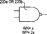
Figure 10 shows the slightly simple HLE 200a (being the simple version of HLE 200 (shown in Figure 3) at least) of a kind of form, and this HLE is used to provide A XOR (XOR) the output Y that B obtains.The interconnection line resource of the actual in this example HLE 200a that uses is drawn with the lines of heavier (thicker).Other existence but the interconnection line resource do not used are in this embodiment represented with the lines of light (thinner).Input A is loaded into the last input of MUX 210.For example, input A can enter HLE200a by programmable links 460 (Fig. 3 illustrates), and described line 460 is shown as in Fig. 3 and is connected on the corresponding MUX input IN0.Input A just can be from the conductor (as 510 among Fig. 8) in the more high-rise interconnection line circuit of device like this.Input A also is loaded on two inputs of NAND door 220b shown in Figure 3.This can cause NAND door 220b with the work of inverter form, as shown in figure 10.The output of inverter 220b (Figure 10) is fed low input to MUX 210 (such as by conductor 322, programmable links 410 (Fig. 3) to one of vertical conductor 240, the part of described vertical conductor, to another programmable links 410 of conductor 360b, and the part of described conductor 360b).
Input B is loaded into the control input end of MUX 210 by conductor 350.For example, input B can be loaded on the conductor 350 by programmable links 460, and described line 460 is illustrated as being connected on the conductor 350 in Fig. 3.Input B just can enter HLE 200a from the more high-rise interconnection line circuit of device like this.When input B was logical zero, MUX 210 was just exported the signal on the last pin (being conductor 360a) that is arranged in two optional input pin.When input B was logical one, MUX 210 was just exported the signal on the next pin (being conductor 360b) that is arranged in two optional input pin.Therefore, the output signal of MUX 210 is exactly A XOR B.
The output signal of MUX 210 is loaded on two inputs of NAND door 220a (Fig. 3), so this NAND door just plays an inverter.The output of NAND door 220a is loaded into rp-drive 230a, and this rp-drive is reverse signal once more.Thereby the effect that element 220a and 230a combine is exactly that output signal for MUX 210 provides a noninverting output driver, i.e. Y (=A XOR B).
The output signal of MUX 210 to the line of two inputs of NAND door 220a can be by the part of conductor 370, one of 250 programmable links 410 (Fig. 3), the part of vertical conductor 250 and the two other programmable links 410 of two inputs from described conductor to NAND door 220a realize from described conductor to vertical conductor.The output Y of driver 220a/230a can be access in more high-rise interconnection line circuit by the programmable links on the output pin of inverter 230a 460 (Fig. 3).
Figure 10 just shows an a kind of example of logic function like this, and this function can realize in single HLE, and the resource of waste is less relatively.In the ASIC LE suitable, realize that same function can make most resource among this ASICLE not be used, thereby cause waste (can only reach result shown in Figure 2) even the logic of employing the above-mentioned type is deleted also with a FPGA LE (with shown in Fig. 1,2 similar).HLE structure herein provides a kind of many implementations of less wastage.
Figure 11 shows the example of another kind of logic function, and this function can realize in single HLE200b (same similar HLE shown in Figure 3 200, or conceptive at least similar).The function that is realized among Figure 11 is Y=(A AND C ') OR (B AND C).The conductor and the element that use in Figure 11 all illustrate with thick line.Conductor that is not used in Figure 11 and element all use thinner lines to illustrate.Signal inserts, by and the mode that picks out HLE 200b can both from explanation above, embody, thereby do not need further detailed description.
Figure 12 shows the example of one four input combination logic function, and this logic function realizes that by two adjacent HLE 200c and 200d wherein each HLE is similar to the HLE 200 shown in Fig. 3, or at least conceptive similar.The logic function that is realized among the figure is F=(A (BC+B ' D)+A ') '.Be used for realizing that the element of this function and conductor all use thicker lines to illustrate in Figure 12.Element that is not used and conductor all use thinner lines to illustrate.Figure 12 has showed and uses potential line to transmit signal from a HLE to another adjacent or close HLE.In this case, the output signal of the MUX 210 among the HLE 200c passes to HLE 200d by the potential line shown in Fig. 3 as 272/314.(visible and be the potential output 272 that how to be connected to right-hand member in the output that this specification had above been narrated MUX 210 from Fig. 3, be connected to the potential input 314 of the HLE on the right again from that, at last the input of the MUX 210 the HLE on the right of described input is connected to.) Figure 12 also showed the VCC input (logical one) of the element 210 that how to use among the HLE 200d and 220a.This can utilize the strip conductor 310 shown in Fig. 3 and realize from the programmable links (such as programmable links 410) that described conductor is connected to the required input end of element 210 and 220a.
Figure 12 shows some the extra interconnection lines between the adjacent HLE of level, their (obviously not illustrating at least) not shown in Figure 3.These lines are the connecting lines more widely of the HLE from each HLE to its right.Fig. 3 shows has only potential line to can be used for this type of connection.But Figure 12 shows 3 signals (output of the output of MUX 210 and NAND door 220a and 220b) that can be delivered to the HLE on the right from each HLE, and the transmission of these signals is to realize on the layer of structure of HLE interconnection resources.This additionally, relatively directly, HLE just makes up a kind of in many feasible way of HLE according to the invention to the connection of HLE.Certainly, if this extra direct connection is provided on the HLE level, also can utilize the interconnection line circuit of higher level to produce similarly connection.Yet, it is believed that at present preferably can provide sufficient, relatively directly, HLE is to the interconnection capability (comprising potential line) of HLE, so that realize the major part (preferably at least be most of) of HLE to the HLE line, described line is needed in order to the one group of HLE that realizes any FPGA LE function.Like this, high-rise interconnection line just can be retained for remote interconnection and use.
Figure 13 shows the example that uses two adjacent HLE 200e and 200f that a trigger or register (one of function of typical FPGA LE) are provided.Equally, HLE 200e and 200f all to Fig. 3 in HLE 200 similar (or at least conceptive similar).The element and the conductor that are used to provide trigger illustrate with thick line in Figure 13.The structure that is not used illustrates with thinner lines.Needn't describe all lines described in Figure 13 herein in detail, or how realize those lines, because from Fig. 3 and explanation above, embodied these information.The signal D that will be deposited can enter HLE200e from the high-rise interconnection line circuit of device or at lower level from another adjacent or close HLE by programmable links 460 (Fig. 3), as long as the explanation this point is just enough.Also be the same for the clock signal clk that drives trigger.(this signal is that HLE 200e and 200f need.) or, CLK also can enter each HLE according to the mode that is used for VCC and VSS shown in Fig. 3.Figure 13 shows CLR ' and SET ' signal, they by conductor 250 and from above or below the programmable links 430 (Fig. 3) of class quasi-conductor in the adjacent HLE enter HLE 200e and 200f.Final these signals can be by entering the HLE array with VCC shown in Fig. 3 and the similar mode of VSS, or the programmable links 460 (Fig. 3) of the high-rise interconnection line circuit by being connected to device.Trigger deposit the high-rise interconnection line circuit that output Q and Q ' can enter device by more programmable links 460, perhaps they also can enter other adjacent or close HLE by the line of lower level.
Figure 14 shows some adjacent HLE 200g, 200h, 200i and 200j, has wherein emphasized some (but inwhole) the direct relatively interconnection resources between the HLE.In the embodiment shown in fig. 14, the interconnection line resource between the HLE comprises the direct line 222 (being shown thick dashed line) of the HLE 200j from the NAND door 220a of HLE 200h to its right.Shown in Figure 14 another direct line is the line 212 (be shown thick dotted line) of the output of the MUX 210 from HLE 200h to the HLE 200j on its right.Shown in the figure another direct line is a potential wire net 214 (being shown heavy line), another HLE (not shown) that this network extends to HLE 200g, 200i and is positioned at HLE 200j the right from the potential output of HLE 200h.In this embodiment, potential output is illustrated as programming and selects from conductor 212 or 222, but also other sources can be used for this signal.All HLE that emphasized among Figure 14 can be implemented in the same one deck metal that is used for HLE interconnector resource to HLE interconnection resources (comprising potential line), therefore just do not need to rely on high-rise interconnection line circuit, the latter to be normally used for the interconnection of long distance.
Figure 15 shows the exemplary arrangement of a HLE 200 on the integrated circuit (IC)-components 500.HLE 200 among Figure 15 can or every otherly herein make up shown in the drawings as Fig. 3, and perhaps they also can comprise any improvement that any place in this specification is mentioned.In exemplary arrangement shown in Figure 15, HLE 200 is arranged on the device 500 with the two-dimensional array form that ranks intersect.Also comprise other circuit in the device 500, as I/O module, memory module or the like (not shown).Therefore ASIC according to the invention can be called as " structured ASIC ", because they have basic circuit organization or structure (such as two-dimentional HLE array shown in Figure 15), and can make self-defining modification and/or interpolation (such as the interconnection line between HLE inside and/or the HLE) to these circuit organizations and structure.If device 500 is not taken as the equivalent product of FPGA and uses, the sum of HLE 200 just can be less than the maximum quantity that LE quantity on the FPGA multiply by the HLE 200 that realizes that FPGA LE all functions are required on the device 500 so.This is because have only the HLE that the function institute that realizes each FPGA LE must quantity to be only necessity, will be less than maximum quantity and in most of the cases will achieve this end required HLE quantity.Along with further specifying hereinafter, some aspect of this point will become clear further.
How the HLE 200 that Figure 16 shows on the device 500 is made separately or together to be used for realizing a LE function among the equivalent FPGA.In Figure 16, the adjacent or close HLE 200 that is used is together stamped same shade, and this is with to be used for other shades adjacent or close HLE different.Quote for convenience, it is 1,2,3 or the like that the HLE among Figure 16 is listed as by label, capable alphabetical A, B, the C or the like of then being put on of HLE.Utilize the reference signs of row and column, Figure 16 shows the HLE that following quilt together uses:
Group 1:A1/A2/B1
Group 2:A3/A4
Group 3:B2/C1/C2/C3
Group 4:B3/B4
Group 5:D1/E1/E2/F1
Group 6:D2/D3/D4
Group 7:F2
Each above-mentioned combination has realized the following function of LE among the equivalent FPGA:
The combinational logic of group 1:FPGA LE A1
The register functions of group 2:FPGA LE A1
The combinational logic of group 3:FPGA LE B1
The register functions of group 4:FPGA LE B1
The combinational logic of group 5:FPGA LE C1
The combinational logic of group 6:FPGA LE D1
The combinational logic of group 7:FPGA LE E1
In above tabulation, row letter and column of figure (similar shown in Figure 16 those) all are used to quote a LE in the two-dimentional FPGA LE array.
Be understandable that HLE grouping example shown in Figure 16 only is exemplary, multiple other grouping is feasible too.The actual packet of (ASIC) employing is by need the equivalent FPGA LE function that realizes determining in ASIC device 500 under specific circumstances.But the preference that the sample list in the first previous paragraphs is advised is as mentioned below.It is more satisfactory for the FPGA LE function in will being implemented in ASIC HLE structure.For example, one or more functions that realized by near the LE the FPGA upper left corner preferably can be realized by the HLE of the necessary amount of (such as near the upper left corner) on the relevant position among the ASIC.
In conjunction with Figure 16, what also will illustrate a bit is that some HLE 200 among the ASIC 500 may not can be used to.
For integrality, Figure 17 shows some the exemplary high-rise interconnection line circuit 510,520 on the ASIC 500.530,540 and 550.For example, circuit 520 can be used to the connection that (on the basis of ASIC customization) produces the I/O port 460 (such as an input) from the I/O port 460 (such as an output) that is positioned near the HLE 200 ASIC 500 upper left corners near another HLE 200 being positioned under the ASIC.For another example, circuit 550 can be used to (on the basis of ASIC customization) and produce connection from the I/O port 460 (such as an output) that is positioned near the HLE 200 the ASIC500 lower left corner to the output port (not shown) of ASIC.Here may need two-layer customizable metal (and intert customizable through hole) that unblock, high-rise wiring is provided, these wirings can enter, draw HLE 200 and/or interconnection between HLE 200 according to any required arrangement.
Comparatively ideal situation is in ASIC design, and the number of plies that needs to customize voluntarily (programming) in the device according to the invention is less relatively.So far mention the layer of programmable via 420/440 (Fig. 4 and Fig. 6) between the vertical and horizontal interconnection line conductor that the layer that needs from customization mainly provide HLE or similar structures in this article, provided the layer of programmable via 470 (Fig. 8) and the layer that high-rise interconnection line circuit itself is provided for the I/O port that is connected high-rise interconnection line circuit.(perhaps, also can always provide whole I/O port through holes 470, when needed they be linked to each other (use) with high-rise interconnection line circuit) in then bypass when not required (not using).
The function that a significant advantage of the present invention is exactly any FPGA LE can be mapped on one or more ASIC HLE (vice versa).So just can provide corresponding to the programming or disposed the ASIC equivalent product (vice versa) of FPGA of Any user based on HLE, and not need on any level (except above mention simply remap) comprehensive user's logic again.This realizes having compared remarkable advantages with the FPGA equivalence that most of structured ASIC manufacturer provides.Usually, this class manufacturer can adopt complicated multi-door or gate array design to come the constitutive logic structure.Because the structure module and the FPGA of these logical constructions are not close,, will carry out comprehensive again if use FPGA to carry out prototype.This ineffective activity will ask extra checking work to guarantee that the design of constructing in the raw product that designs among the FPGA and the structured ASIC is identical on function.If produce a FPGA of programming with this structured ASIC equivalence, the weight of logic comprehensively is necessary too.The present invention avoided dispose when moving between FPGA and the ASIC based on HLE required this comprehensive again.In addition, compare with the ASIC LE of similar FPGA LE on the structure, HLE also saved the space (because for each FPGA LE, have only the function that realizes the corresponding FPGA LE that programmed must quantity HLE just be used).
Figure 18 shows a series of exemplary flow process unit (being step and/or result), these flow process unit can be used to produce corresponding to equivalence based on the FPGA of LE and based on the design of the ASIC of HLE.Figure 18 shows and at first produces a FPGA design, and then the ASIC design that is produced a roughly equiv by described FPGA design.The necessary logic of user's appointment (and other possible functions) is shown in the flow process unit 610, and typical canonical form is RTL (a register transfer level).In flow process unit 620, the form (such as LE that comprises 4-LUT and register or the like) that described RTL can be realized in having the FPGA of particular characteristics by comprehensive one-tenth by the general relatively standard that is provided in the flow process unit 610.Flow process unit 620 can utilize commercial FPGA integrated software instrument to finish, such as being positioned at California, the Quatus II product that altera corp provided of San Jose.Comprehensive 620 results that obtain then are mapped in flow process unit 630 in the specific FPGA product.
Next flow process unit 640 is that the FPGA mapping is converted to net list and layout information corresponding to specific FPGA, and described specific FPGA belongs within the contemplated general FPGA product scope in flow process unit 630.For example, flow process unit 640 can be operated among the FPGA of the resource with specific quantity and structure.Flow process unit 640 has been stipulated which in these resources to realize each function of user's design with.The FPGA of particular type can programme by bit stream according to the information that produces in flow process unit 640.
In order to produce a ASIC based on HLE equivalent substantially with the FPGA that programmes according to information 640, be according to the present invention to 640 information and executing steps 650.Step 650 is a kind of 1 pair 1 functional unit mappings, and it is mapped as one or one group of HLE with the functional unit in 640 information, and these HLE can realize described functional unit with minimizing.In the example that this specification is above discussed, described functional unit or be the combinational logic that LUT realized among the given FPGA LE, or be register among the given FPGA LE.If described functional unit is a combinational logic, step 650 is to realize the HLE of the minimum number of described function with this logical mappings just so.Wherein preferably include and adopt above-mentioned logic to delete to reduce required selection progression.Other technologies also can be used to simplify the logic that realizes among (optimization) HLE.If described functional unit is a register, step 650 just is two HLE with this register mappings so, just as shown in Figure 13.Step 650 is also selected to allow which HLE realize which functional unit, and how each HLE should be disposed so that allow this HLE can realize its effect in the functional unit that is assigned to.For example, step 650 to the ASIC of equivalence the time, is preferably keeping general function distribution (but keep general location is not essential, and the HLE of equivalence can be placed in other parts of target ASIC) with the functional localization on the FPGA.Step 650 has also been stipulated high-rise wiring, and in order to introducing being provided, drawing HLE or HLE group and/or line between HLE or HLE group, these lines normally can not be lower, comparatively directly, provide on the level between HLE.Supposed in the explanation that more than step 650 is to realize carrying out among the ASIC of defined function among the initial FPGA having enough capacity.
The result 660 of step 650 is ASIC net list and layout information, and these information can be used to regulation and make the required mask of ASIC, described ASIC on function with initial FPGA (by 640 information specifies) equivalence.More favourable a bit is that described 660 information are directly to obtain from 640 information.Carry out FPGA in the conversion of ASIC like this, just do not needing again comprehensive user's initial logical specification (such as such in step 620).Therefore just can there be defective according to FPGA that step and result produced shown in Figure 180 and the equivalence between the ASIC.
Figure 19 show another according to the invention be used to produce equivalence based on the FPGA of LE and technology based on the ASIC of HLE.Flow process unit 710 to 720 respectively to Figure 18 in flow process unit 610 similar with 620.Comprehensive 720 the result who is associated with specific FPGA technology is used to produce user logic and is designed into FPGA device and user logic and is designed into mapping based on the ASIC device of HLE.In other words, a kind of general logic synthesis 720 is used as the common base of mapping 730 and 750.The logically equivalent of these two kinds of mappings just is guaranteed.FPGA mapping 730 is utilized for specific FPGA design and produces net list and layout information (i.e. programming or configuration).The mask able to programme based on the ASIC of HLE that 750 of ASIC mappings are utilized for a specific mask-programmable produces standard 760.The FPGA that produces according to information 740 logically is equivalent to the ASIC that produces according to information 760, and vice versa.For example, if only produced the ASIC version at the beginning, but kept the FPGA mapping 730 or the FPGA information 740 that obtain according to initial comprehensive 720, need not so again comprehensive, and as long as use information 740 or shine upon 730 (producing information 740 once more) and just can obtain FPGA with the ASIC equivalence.This point has supposed here that for same being suitable for for Equivalent A SIC required after the FPGA that at first produces is transformed into the mapping 750 of initial generation or information 760 all have been retained.According to information 760 or shine upon 750 (being taken as the basis that is used for producing once more information 760 now), can at any time produce ASIC.It is comprehensive again to need not to carry out logic, and the equivalence between ASIC that produces afterwards and the initial FPGA that produces is also guaranteed.
Figure 20 shows and another kind of according to the inventionly produces technology based on the FPGA of LE according to existing ASIC based on HLE.Equally, the flow process unit 810 and 820 among Figure 20 is similar to the flow process unit 610 and 620 (or the flow process unit 710 and 720 among Figure 19) among Figure 18 respectively.Technology-mapped 830 is associated with FPGA system based on LE, but it utilizes HLE storehouse 840 to carry out a step, and this step can be produced the mapping based on HLE by the mapping based on FPGA LE.Flow process unit 850 be standard of mask generation able to programme based on the ASIC of HLE of mask-programmable according to mapping 830.ASIC can produce according to this standard.
If need the FPGA of an equivalence from now on, just can produce this FPGA, just as further illustrating among Figure 20 according to information 850.In flow process unit 860, information 850 remaps back based on the form of LE from the form based on HLE.This mapping can be to organize 1 couple, 1 mapping of getting back to LE from each HLE or HLE, and described HLE or HLE group are to obtain according to the LE function in unit 830 and 840, and described LE then is the LE that has described function at first.For the ease of carrying out this 1 pair 1 mapping, can comprise a record in the information 850, the various piece of wherein having put down in writing it is how to get from initial LE.In flow process unit 860, do not need logic comprehensive again.According to unit 860, just can obtain the single and layout information 870 of FPGA net, and this information can be used to produce and the logically equivalent FPGA of ASIC that obtains according to information 850.
Although hint to some extent at least that in preamble will spell out, technology-mapped 830 can not at random make up the logical design that HLE realizes the user here.On the contrary, mapping 830 only limits to use HLE to realize the function that can realize in FPGA LE.This carries out 1 pair 1 mapping 860 to information 850 after making in unit 870, so that its form of shining upon back based on LE is become possibility.
Figure 21 a-c, 22a-c and 23 show NAND array 220 among as shown in Figure 3 the HLE and possible other elements 230 (or equivalent electric circuit) can be according to the present invention other aspect contents carry out the example of various configurations (for example, masking film program).For example, Figure 21 a-c shows the various forms that inverter is provided.In Figure 21 a, an input of a NAND door 220 is bound to be logical one.In Figure 21 b, used an inverter 230.In Figure 21 c, NAND door 220a and 220b or two inverter 230a and 230b are by (by the interconnection line resource among the HLE is carried out appropriate masking film program) in parallel, so that a bigger inverter to be provided effectively, provide stronger output to drive from HLE such as being used for.
Figure 22 a-c shows the some examples how non-return buffer is provided.In Figure 22 a, NAND door 220a and 220b are contacted, and wherein each NAND door all has an input to be bound to logical one.Equally, the interconnection resource of HLE by masking film program with the described NAND door of contacting.In Figure 22 b, inverter 230a and 230b are contacted equally.In Figure 22 c, NAND door 220a and b are with the parallel connection of inverter form (as shown in Figure 21 a), so that first a bigger inverter 220a/b to be provided effectively, and inverter 230a and b are by same in parallel so that second a bigger inverter 230a/b to be provided effectively.As shown in Figure 21 c, provide stronger output to drive than big unit from HLE among Figure 22 c.
Figure 23 shows of using among NAND door 220a or the 220b NAND is provided function.
The motivation of making some selection in the multiple option shown in Figure 21-23 may be to use the outputs that provide difference to measure for different HLE in the device of HLE according to the invention to drive at certain.The driver of certain size can drive the parasitic load of some usually.In the ASIC flow process, to such an extent as to, often just must or wish increase standard cell or metal-programmable unit or inserting another driver (buffer or inverter) promotes actuating force if output quantity very huge original driver element can not drive load.This means that size increases or increase the expansion that buffer/inverter can cause area.Yet, use the ASIC based on HLE according to the invention, just can utilize the unit (HLE or section H LE) that is not used to promote actuating force (noninverting or anti-phase) easily, such as passing through low layer programmable interconnection resource.In various different configurations-such as in Figure 21-23, show those-unit (as 220 and/or 230) that can together use just needn't be arranged in identical HLE.They can be in adjacent or close HLE.
Just mentioned in as mentioned like that, can use various technology to save and realize the required HLE quantity of some function.As mentioned above, logic deletes it is an example of this class HLE saving technique.Another example is that a HLE drives another HLE, and second HLE is set to such as one 2 input NAND door.If this thing happens, the ASIC flow process just can be included in described NAND door among first HLE so, thereby HLE quantity is kept to one from two.Many analogous cases are arranged, and wherein n HLE can be involved in n-1 HLE, and n-1 HLE can be involved in n-2 HLE, or the like, particularly under the situation that comprises inverter 230 as shown in Figure 3.Other examples also comprise (! A AND B), (A AND B) or the like.
Be appreciated that above explanation is the example of the principle of the invention, and those people that are proficient in present technique can make various improvement under the prerequisite that does not depart from the scope of the invention and guiding theory.For example, described herein FPGA and ASIC need not to be pure FPGA or ASIC.A device can partly be that FPGA or part are ASIC and other parts (such as part FPGA and part A SIC).The FPGA of indication and ASIC can be understood that the FPGA or the ASIC part of this class hybrid device herein.
Although mainly illustrated herein with through hole programming (referring to for example Fig. 4-9) carry out that logic makes up and HLE in, wiring between HLE, but the programming (such as utilizing the optional line of metal, fuse, anti-fuse, CRAM control, Flash control or the like) that is appreciated that other types also can be used as and substitute or replenish.If used in the described other technologies certain some, so above described masking film program just can be considered to refer to these other programming techniques, and these technology can realize by other modes except customizing or partly customize certainly mask certainly.Equally, although HLE herein is described for realizing and the function of FPGA LE equivalence that the HLE shown in is the high performance element of high density herein.Therefore they can be used to equally constitute high performance intellectual property (IP) (such as Digital Signal Processing (DSP) module, microprocessor, or the like), memory, or the like.
Claims (58)
1. logic unit circuit comprises:
Select circuit, it utilizes the first selection circuit input signal that is input to this selection circuit to select the second and the 3rd to select a conduct in the circuit input signal to select circuit output signal;
Be used to provide the logical circuit of a logic circuit output signal, described output signal is the logical function of first and second logical circuit input signal; And
Programmable interconnect line circuit, this circuit make in first and second logical circuit input signal at least one to obtain from described selection circuit output signal or the signal from the logical block outside.
2. circuit according to claim 1, wherein said selection circuit comprises the MUX circuit.
3. circuit according to claim 1, wherein said logical circuit comprises the NAND circuit.
4. circuit according to claim 1, wherein said programmable interconnect line circuit comprises the mask-programmable circuit.
5. circuit according to claim 1, wherein said programmable circuit comprises the programmable via circuit.
6. circuit according to claim 1 also comprises:
Other programmable interconnect line circuits are used for allowing first, second and third at least one that select circuit input signal obtain from described logic circuit output signal.
7. circuit according to claim 6 also comprises:
Extra programmable interconnect line circuit is used for allowing first, second and third at least one that select circuit input signal obtain from a signal from the logical block outside.
8. circuit according to claim 1 also comprises:
Other logical circuits are used to provide other logic circuit output signal, and described output signal is the logical function of first and second other logical circuit input signals.
9. circuit according to claim 8 also comprises:
Other programmable interconnect line circuits, be used for allowing first and second other logical circuit input signals at least one can from described selection circuit output signal or the signal from the logical block outside draws.
10. circuit according to claim 8 also comprises:
Other programmable interconnect line circuits are used for allowing at least one of first and second other logical circuit input signals draw from described logic circuit output signal.
11. circuit according to claim 10 also comprises:
Extra programmable interconnect line circuit is used for allowing at least one of first and second other logical circuit input signals draw from described selection circuit output signal or from a signal from the logical block outside.
12. an integrated circuit (IC)-components comprises:
A plurality of logic unit circuits, each unit is all as claimed in claim 1 the same.
13. device according to claim 12 also comprises:
Other programmable interconnect line circuits are used for allowing being loaded into another logic unit circuit in a plurality of logic unit circuits adjacent with above-mentioned logic unit circuit from each signal of the described logic unit circuit of at least a portion.
14. device according to claim 13, wherein said programmable interconnect line circuit are set in the first subclass layer of described device, and wherein said other programmable interconnect line circuits also are set in the first subclass layer of described device.
15. device according to claim 14 also comprises:
Extra programmable interconnect line circuit, be used for allowing from each signal of the described logic unit circuit of at least a portion be loaded into the non-conterminous a plurality of logic unit circuits of described logic unit circuit in another logic unit circuit.
16. device according to claim 15, wherein said extra programmable interconnect line circuit are set in the layer of the first subclass layer that is not in the described device at least in part.
17. method of utilizing the ASIC architecture to design the ASIC that is equivalent to FPGA substantially, comprise a plurality of HLE in the described ASIC architecture, each HLE can both provide the part of functions of the LE of described FPGA, and these HLE can be combined in where necessary and come together to realize the existing repertoire of any one LE institute the subject of knowledge and the object of knowledge, and described method comprises:
Comprehensive user logic design;
Logical design after comprehensive is mapped as a FPGA design; And
Each LE in the FPGA design is remapped to one or more HLE in the ASIC design.
18. method according to claim 17, wherein said mapping comprises:
Generate FPGA net list and layout information.
19. method according to claim 18, wherein said remapping carried out described FPGA net list and layout information.
20. method according to claim 17, wherein said remapping comprises:
Produce ASIC net list and layout information.
21. method according to claim 19, wherein said remapping comprises:
Produce ASIC net list and layout information.
22. the ASIC that utilizes the method described in the claim 17 to make.
23. method according to claim 17, wherein said remapping comprises:
Utilize a plurality of HLE adjacent one another are realize single HLE the function of irrealizable any LE.
24. method according to claim 17, wherein said remapping comprises:
When being remapped to one or more HLE, the function with FPGA LE use logic to delete.
25. method according to claim 17, wherein said remapping comprises:
(1) logic function of each FPGA LE further is remapped to each different HLE or HLE group with (2) register functions.
26. method of utilizing the ASIC architecture to design the FPGA and the ASIC of basic equivalence, comprise a plurality of HLE in the described architecture, each HLE can both provide the part of functions of the LE of FPGA, and these HLE can be combined in where necessary and come together to realize the existing repertoire of any one LE institute the subject of knowledge and the object of knowledge, and described method comprises:
Comprehensive user's logical design;
To be mapped as a FPGA design through comprehensive logical design; And
To be mapped as an ASIC design through comprehensive logical design.
27. method according to claim 26, the wherein said FPGA of being mapped as design comprises:
Generate FPGA net list and layout information.
28. method according to claim 26, the wherein said ASIC of being mapped as design comprises:
Generate ASIC net list and layout information.
29. the ASIC that utilizes the described method of claim 26 to make.
30. method according to claim 26, the wherein said ASIC of being mapped as design comprises:
Use a plurality of HLE to realize the function of FPGA LE.
31. method according to claim 30, wherein said use comprises:
Use a plurality of HLE adjacent one another are to realize the function of any LE that single HLE can't realize.
32. method according to claim 30, wherein said use comprises:
Use logic to delete the function of helping realize a FPGA LE with one or more HLE.
33. method according to claim 30, wherein said use comprises:
HLE that use differs from one another or HLE organize (1) logic function and (2) register functions that realizes a FPGA LE.
34. a design is equivalent to the method for the FPGA of ASIC, comprise a plurality of HLE in the structure of described ASIC, each HLE can provide the part of functions of FPGA LE, and the described HLE repertoire that any one LE of realization can realize that can be combined where necessary, described method comprises:
Comprehensive user's logical design; And
To use HLE to realize FPGA LE function, will be mapped as an ASIC design through comprehensive logical design.
35. a design is equivalent to the method for the FPGA of ASIC, comprise a plurality of HLE in the structure of described ASIC, each HLE can both structure provides the partial function of FPGA LE, and these HLE can be combined in where necessary and come together to realize the repertoire that any one LE can realize, described method comprises:
Comprehensive user's logical design;
To use HLE to realize FPGA LE function, will be mapped as an ASIC design through comprehensive logical design; And
The ASIC design is remapped to the FPGA design.
36. method according to claim 35, wherein said mapping comprises:
Generate ASIC net list and layout information.
37. method according to claim 36, wherein said remapping carried out described FPGA net list and layout information.
38. method according to claim 35, wherein said remapping comprises:
Produce FPGA net list and layout information.
39. according to the described method of claim 37, wherein said remapping comprises:
Generate FPGA net list and layout information.
40. the FPGA that utilizes the described method of claim 35 to make.
41. method according to claim 35, wherein said mapping comprises:
Utilize a plurality of HLE adjacent one another are realize single HLE the function of irrealizable any LE.
42. according to the described method of claim 41, wherein said mapping also comprises:
Write down which HLE made together be used for realizing single HLE the function of irrealizable any LE.
43. according to the described method of claim 42, wherein said remapping also comprises:
Utilize described record to discern the HLE group and be each LE to remap.
44. method according to claim 35, wherein said mapping comprises:
When utilizing HLE to realize the function of at least a portion FPGA LE, the utilization logic is deleted.
45. method according to claim 35, wherein said mapping comprises:
(1) logic function and (2) register functions of each FPGA LE further are mapped to each different HLE or HLE group.
46. an ASIC who on function, is equivalent to the FPGA that programmed, comprising:
A plurality of HLE, each HLE also can only realize the part of functions of a LE who is fully utilized among the FPGA under situation about being fully utilized, the function of each described LE is mapped to a corresponding HLE or HLE group.
47. logic unit circuit, its combinational logic ability mainly comprise single input lut circuits and two the two input NAND doors or the logically equivalent circuit of this class NAND door.
48. according to the described circuit of claim 47, wherein said lut circuits comprises:
Have two optional inputs and a MUX circuit of selecting the control input end.
49., also comprise according to the described circuit of claim 47:
The programmable interconnect line circuit is used for selectively signal being introduced, being drawn described lut circuits and NAND door or their logically equivalent circuit, and transmits signal between described circuit.
50., also comprise according to the described circuit of claim 47:
Output buffer circuit.
51., also comprise according to the described circuit of claim 50:
The programmable interconnect line circuit is used for selectively the output signal of described lut circuits or at least one NAND door or described logically equivalent circuit is loaded into described output buffer circuit.
52. according to the described circuit of claim 49, wherein said programmable interconnect line circuit is the part mask-programmable at least.
53. according to the described circuit of claim 49, wherein said programmable interconnect line circuit is that partial through holes is programmable at least.
54. an ASIC who comprises a plurality of logic unit circuits, each logic unit circuit is described the same with claim 47.
55. according to the described ASIC of claim 54, all functions of each logical block on function among the FPGA of equivalence are all realized by a described corresponding logic unit circuit or logic unit circuit group.
56. a structured ASIC that comprises HLE, wherein said structured ASIC can realize being the logic of FPGA LE comprehensively.
57. according to the described structured ASIC of claim 56, wherein said logic is mapped as LE, is remapped back HLE again.
58. according to the described structured ASIC of claim 56, the repertoire of wherein said each LE is all finished alone or in combination by HLE.
Applications Claiming Priority (2)
| Application Number | Priority Date | Filing Date | Title |
|---|---|---|---|
| US10/884,460 | 2004-07-02 | ||
| US10/884,460 US7243329B2 (en) | 2004-07-02 | 2004-07-02 | Application-specific integrated circuit equivalents of programmable logic and associated methods |
Publications (1)
| Publication Number | Publication Date |
|---|---|
| CN1716781A true CN1716781A (en) | 2006-01-04 |
Family
ID=34993053
Family Applications (1)
| Application Number | Title | Priority Date | Filing Date |
|---|---|---|---|
| CN 200510072989 Pending CN1716781A (en) | 2004-07-02 | 2005-05-25 | Application-specific integrated circuit equivalents of programmable logic and associated methods |
Country Status (4)
| Country | Link |
|---|---|
| US (5) | US7243329B2 (en) |
| EP (1) | EP1612940A3 (en) |
| JP (5) | JP5036146B2 (en) |
| CN (1) | CN1716781A (en) |
Cited By (3)
| Publication number | Priority date | Publication date | Assignee | Title |
|---|---|---|---|---|
| CN103155414A (en) * | 2010-08-06 | 2013-06-12 | 阿尔特拉公司 | Hardened programmable devices |
| CN101272141B (en) * | 2007-03-21 | 2015-11-25 | 阿尔特拉公司 | Staggered logic array block architecture |
| CN105281892A (en) * | 2014-06-03 | 2016-01-27 | 英派尔科技开发有限公司 | Perturbation of field programmable gate array code to prevent side channel attack |
Families Citing this family (32)
| Publication number | Priority date | Publication date | Assignee | Title |
|---|---|---|---|---|
| US7373631B1 (en) * | 2004-08-11 | 2008-05-13 | Altera Corporation | Methods of producing application-specific integrated circuit equivalents of programmable logic |
| US7392498B1 (en) * | 2004-11-19 | 2008-06-24 | Xilinx, Inc | Method and apparatus for implementing a pre-implemented circuit design for a programmable logic device |
| US7441223B1 (en) * | 2005-01-07 | 2008-10-21 | Altera Corporation | Method and apparatus for performing synthesis to improve density on field programmable gate arrays |
| US7620924B2 (en) * | 2005-03-14 | 2009-11-17 | Lsi Corporation | Base platforms with combined ASIC and FPGA features and process of using the same |
| US7275232B2 (en) * | 2005-04-01 | 2007-09-25 | Altera Corporation | Methods for producing equivalent field-programmable gate arrays and structured application specific integrated circuits |
| US7304497B2 (en) * | 2005-04-29 | 2007-12-04 | Altera Corporation | Methods and apparatus for programmably powering down structured application-specific integrated circuits |
| US7404169B2 (en) * | 2005-05-31 | 2008-07-22 | Altera Corporation | Clock signal networks for structured ASIC devices |
| US7386819B1 (en) * | 2005-07-28 | 2008-06-10 | Altera Corporation | Methods of verifying functional equivalence between FPGA and structured ASIC logic cells |
| US7373630B1 (en) | 2005-12-12 | 2008-05-13 | Altera Corporation | Methods for improved structured ASIC design |
| US8037444B1 (en) | 2006-07-20 | 2011-10-11 | Altera Corporation | Programmable control of mask-programmable integrated circuit devices |
| US7587686B1 (en) | 2006-08-01 | 2009-09-08 | Altera Corporation | Clock gating in a structured ASIC |
| US7472370B1 (en) | 2006-08-11 | 2008-12-30 | Xilinx, Inc. | Comparing graphical and netlist connections of a programmable logic device |
| US7536668B1 (en) | 2006-08-11 | 2009-05-19 | Xilinx, Inc. | Determining networks of a tile module of a programmable logic device |
| US7451423B1 (en) | 2006-08-11 | 2008-11-11 | Xilinx, Inc. | Determining indices of configuration memory cell modules of a programmable logic device |
| US7451425B1 (en) | 2006-08-11 | 2008-11-11 | Xilinx, Inc. | Determining controlling pins for a tile module of a programmable logic device |
| US7584448B1 (en) * | 2006-08-11 | 2009-09-01 | Xilinx, Inc. | Constructing a model of a programmable logic device |
| US7451420B1 (en) | 2006-08-11 | 2008-11-11 | Xilinx, Inc. | Determining reachable pins of a network of a programmable logic device |
| US7451424B1 (en) | 2006-08-11 | 2008-11-11 | Xilinx, Inc. | Determining programmable connections through a switchbox of a programmable logic device |
| US7478359B1 (en) * | 2006-10-02 | 2009-01-13 | Xilinx, Inc. | Formation of columnar application specific circuitry using a columnar programmable logic device |
| US7589555B1 (en) * | 2007-01-08 | 2009-09-15 | Altera Corporation | Variable sized soft memory macros in structured cell arrays, and related methods |
| JP2008192967A (en) * | 2007-02-07 | 2008-08-21 | Elpida Memory Inc | Semiconductor device and wiring switching option thereof |
| US7924052B1 (en) | 2008-01-30 | 2011-04-12 | Actel Corporation | Field programmable gate array architecture having Clos network-based input interconnect |
| US7586327B1 (en) | 2008-03-25 | 2009-09-08 | Altera Corporation | Distributed memory circuitry on structured application-specific integrated circuit devices |
| US7622952B1 (en) | 2008-05-28 | 2009-11-24 | Altera Corporation | Periphery clock signal distribution circuitry for structured ASIC devices |
| JP5453850B2 (en) * | 2009-03-06 | 2014-03-26 | 富士通セミコンダクター株式会社 | Semiconductor integrated circuit |
| WO2012032937A1 (en) * | 2010-09-08 | 2012-03-15 | 日本電気株式会社 | Reconfigurable circuit |
| WO2012047735A2 (en) * | 2010-09-29 | 2012-04-12 | The Regents Of The University Of California | In-place resynthesis and remapping techniques for soft error mitigation in fpga |
| US8533641B2 (en) | 2011-10-07 | 2013-09-10 | Baysand Inc. | Gate array architecture with multiple programmable regions |
| US20180062654A9 (en) * | 2011-11-30 | 2018-03-01 | Agate Logic Inc. | Method and apparatus for facilitating communication between programmable logic circuit and application specific integrated circuit with clock adjustment |
| US20160239313A1 (en) * | 2013-11-08 | 2016-08-18 | Empire Technology Development Llc | Control of router in cloud system |
| US10394991B2 (en) * | 2016-10-06 | 2019-08-27 | Altera Corporation | Methods and apparatus for dynamically configuring soft processors on an integrated circuit |
| US10353709B2 (en) * | 2017-09-13 | 2019-07-16 | Nextera Video, Inc. | Digital signal processing array using integrated processing elements |
Family Cites Families (53)
| Publication number | Priority date | Publication date | Assignee | Title |
|---|---|---|---|---|
| US4910417A (en) * | 1986-09-19 | 1990-03-20 | Actel Corporation | Universal logic module comprising multiplexers |
| US5451887A (en) * | 1986-09-19 | 1995-09-19 | Actel Corporation | Programmable logic module and architecture for field programmable gate array device |
| JPH03139863A (en) * | 1989-10-25 | 1991-06-14 | Hitachi Ltd | Semiconductor integrated circuit |
| JPH046913A (en) * | 1990-04-24 | 1992-01-10 | Kawasaki Steel Corp | Programmable logic element |
| US5068547A (en) * | 1990-09-05 | 1991-11-26 | Lsi Logic Corporation | Process monitor circuit |
| US5717928A (en) * | 1990-11-07 | 1998-02-10 | Matra Hachette Sa | System and a method for obtaining a mask programmable device using a logic description and a field programmable device implementing the logic description |
| US5122685A (en) * | 1991-03-06 | 1992-06-16 | Quicklogic Corporation | Programmable application specific integrated circuit and logic cell therefor |
| JPH05252025A (en) * | 1991-10-28 | 1993-09-28 | Texas Instr Inc <Ti> | Logic module and integrated circuit |
| JPH06176102A (en) * | 1992-10-09 | 1994-06-24 | Ricoh Co Ltd | Net list generation device for gate array |
| US5550839A (en) * | 1993-03-12 | 1996-08-27 | Xilinx, Inc. | Mask-programmed integrated circuits having timing and logic compatibility to user-configured logic arrays |
| JPH0785115A (en) * | 1993-09-10 | 1995-03-31 | Toshiba Corp | Data logger for checking logic circuit and method for logging check data |
| KR960002333B1 (en) * | 1993-12-23 | 1996-02-16 | 재단법인한국전자통신연구소 | Logic integrated circuit module |
| TW396312B (en) * | 1993-12-30 | 2000-07-01 | At & T Corp | Method and apparatus for converting field-programmable gate array implementations into mask-programmable logic cell implementations |
| US5502402A (en) * | 1995-01-05 | 1996-03-26 | Texas Instruments Incorporated | FPGA architecture based on a single configurable logic module |
| US5671432A (en) * | 1995-06-02 | 1997-09-23 | International Business Machines Corporation | Programmable array I/O-routing resource |
| JP3072888B2 (en) * | 1995-12-14 | 2000-08-07 | 川崎製鉄株式会社 | Field programmable gate array |
| US5841295A (en) * | 1996-02-09 | 1998-11-24 | Hewlett-Packard Company | Hybrid programmable logic device |
| US5894565A (en) | 1996-05-20 | 1999-04-13 | Atmel Corporation | Field programmable gate array with distributed RAM and increased cell utilization |
| US5825202A (en) | 1996-09-26 | 1998-10-20 | Xilinx, Inc. | Integrated circuit with field programmable and application specific logic areas |
| US5963050A (en) | 1997-02-26 | 1999-10-05 | Xilinx, Inc. | Configurable logic element with fast feedback paths |
| US5874834A (en) | 1997-03-04 | 1999-02-23 | Xilinx, Inc. | Field programmable gate array with distributed gate-array functionality |
| JPH10320451A (en) * | 1997-05-21 | 1998-12-04 | Hitachi Telecom Technol Ltd | Net data preparation method for gate array |
| US6097212A (en) * | 1997-10-09 | 2000-08-01 | Lattice Semiconductor Corporation | Variable grain architecture for FPGA integrated circuits |
| JP3123977B2 (en) | 1998-06-04 | 2001-01-15 | 日本電気株式会社 | Programmable function block |
| US6150838A (en) | 1999-02-25 | 2000-11-21 | Xilinx, Inc. | FPGA configurable logic block with multi-purpose logic/memory circuit |
| EP1161797B1 (en) * | 1999-03-11 | 2004-12-22 | Easic Corporation | Integrated circuit technology |
| US6294926B1 (en) * | 1999-07-16 | 2001-09-25 | Philips Electronics North America Corporation | Very fine-grain field programmable gate array architecture and circuitry |
| US6331790B1 (en) * | 2000-03-10 | 2001-12-18 | Easic Corporation | Customizable and programmable cell array |
| US6629294B2 (en) * | 2000-03-10 | 2003-09-30 | General Electric Company | Tool and method for improving the quality of board design and modeling |
| US6490707B1 (en) | 2000-07-13 | 2002-12-03 | Xilinx, Inc. | Method for converting programmable logic devices into standard cell devices |
| US6526563B1 (en) | 2000-07-13 | 2003-02-25 | Xilinx, Inc. | Method for improving area in reduced programmable logic devices |
| US6515509B1 (en) | 2000-07-13 | 2003-02-04 | Xilinx, Inc. | Programmable logic device structures in standard cell devices |
| DE60228083D1 (en) * | 2001-05-16 | 2008-09-18 | Nxp Bv | RECONFIGURABLE LOGIC DEVICE |
| US6580289B2 (en) * | 2001-06-08 | 2003-06-17 | Viasic, Inc. | Cell architecture to reduce customization in a semiconductor device |
| US6769107B1 (en) * | 2001-12-03 | 2004-07-27 | Lsi Logic Corporation | Method and system for implementing incremental change to circuit design |
| US6911842B1 (en) * | 2002-03-01 | 2005-06-28 | Xilinx, Inc. | Low jitter clock for a physical media access sublayer on a field programmable gate array |
| JP2003273727A (en) * | 2002-03-14 | 2003-09-26 | Shinji Kimura | Semiconductor integrated circuit device |
| JP3860812B2 (en) * | 2002-04-17 | 2006-12-20 | 富士通株式会社 | Concurrent development support program, development support method, and development support apparatus for ASIC and programmable logic device |
| US6759869B1 (en) * | 2002-06-05 | 2004-07-06 | Xilinx, Inc. | Large crossbar switch implemented in FPGA |
| US6873185B2 (en) * | 2002-06-19 | 2005-03-29 | Viasic, Inc. | Logic array devices having complex macro-cell architecture and methods facilitating use of same |
| US7112994B2 (en) * | 2002-07-08 | 2006-09-26 | Viciciv Technology | Three dimensional integrated circuits |
| US7064579B2 (en) * | 2002-07-08 | 2006-06-20 | Viciciv Technology | Alterable application specific integrated circuit (ASIC) |
| US7679398B2 (en) * | 2002-07-17 | 2010-03-16 | Osann Jr Robert | Reprogrammable instruction DSP |
| US7346876B2 (en) * | 2002-09-04 | 2008-03-18 | Darien K. Wallace | ASIC having dense mask-programmable portion and related system development method |
| US6829756B1 (en) * | 2002-09-23 | 2004-12-07 | Xilinx, Inc. | Programmable logic device with time-multiplexed interconnect |
| US6988258B2 (en) | 2002-12-09 | 2006-01-17 | Altera Corporation | Mask-programmable logic device with building block architecture |
| US6870395B2 (en) * | 2003-03-18 | 2005-03-22 | Lattice Semiconductor Corporation | Programmable logic devices with integrated standard-cell logic blocks |
| WO2005001724A2 (en) | 2003-06-23 | 2005-01-06 | Altera Corporation | Method for programming a mask-programmable logic device and device so programmed |
| US7038490B1 (en) * | 2003-09-12 | 2006-05-02 | Lattice Semiconductor Corporation | Delay-matched ASIC conversion of a programmable logic device |
| US7003746B2 (en) * | 2003-10-14 | 2006-02-21 | Hyduke Stanley M | Method and apparatus for accelerating the verification of application specific integrated circuit designs |
| US7019557B2 (en) * | 2003-12-24 | 2006-03-28 | Viciciv Technology | Look-up table based logic macro-cells |
| US7100142B2 (en) * | 2004-04-07 | 2006-08-29 | Synopsys, Inc. | Method and apparatus for creating a mask-programmable architecture from standard cells |
| US7081772B1 (en) | 2004-06-04 | 2006-07-25 | Altera Corporation | Optimizing logic in non-reprogrammable logic devices |
-
2004
- 2004-07-02 US US10/884,460 patent/US7243329B2/en not_active Expired - Fee Related
-
2005
- 2005-05-25 CN CN 200510072989 patent/CN1716781A/en active Pending
- 2005-06-24 EP EP05253922A patent/EP1612940A3/en not_active Withdrawn
- 2005-07-01 JP JP2005193749A patent/JP5036146B2/en not_active Expired - Fee Related
-
2007
- 2007-05-07 US US11/801,082 patent/US7870513B2/en not_active Expired - Fee Related
-
2010
- 2010-12-14 US US12/967,851 patent/US8291355B2/en not_active Expired - Fee Related
-
2012
- 2012-04-06 JP JP2012087199A patent/JP5475045B2/en not_active Expired - Fee Related
- 2012-07-09 JP JP2012153545A patent/JP5623471B2/en not_active Expired - Fee Related
- 2012-09-13 US US13/614,819 patent/US8504963B2/en active Active
-
2013
- 2013-07-31 US US13/955,200 patent/US8863061B2/en not_active Expired - Fee Related
-
2014
- 2014-04-11 JP JP2014081749A patent/JP2014131365A/en not_active Withdrawn
- 2014-10-10 JP JP2014208874A patent/JP5859089B2/en not_active Expired - Fee Related
Cited By (5)
| Publication number | Priority date | Publication date | Assignee | Title |
|---|---|---|---|---|
| CN101272141B (en) * | 2007-03-21 | 2015-11-25 | 阿尔特拉公司 | Staggered logic array block architecture |
| CN103155414A (en) * | 2010-08-06 | 2013-06-12 | 阿尔特拉公司 | Hardened programmable devices |
| US9654109B2 (en) | 2010-08-06 | 2017-05-16 | Altera Corporation | Hardened programmable devices |
| CN105281892A (en) * | 2014-06-03 | 2016-01-27 | 英派尔科技开发有限公司 | Perturbation of field programmable gate array code to prevent side channel attack |
| CN105281892B (en) * | 2014-06-03 | 2018-11-02 | 英派尔科技开发有限公司 | The perturbation of field programmable gate array code is to prevent side channel analysis |
Also Published As
| Publication number | Publication date |
|---|---|
| US8504963B2 (en) | 2013-08-06 |
| JP2006020329A (en) | 2006-01-19 |
| JP2014131365A (en) | 2014-07-10 |
| US20060001444A1 (en) | 2006-01-05 |
| EP1612940A2 (en) | 2006-01-04 |
| US8291355B2 (en) | 2012-10-16 |
| US7870513B2 (en) | 2011-01-11 |
| JP2015008539A (en) | 2015-01-15 |
| JP5036146B2 (en) | 2012-09-26 |
| US20070210827A1 (en) | 2007-09-13 |
| JP5859089B2 (en) | 2016-02-10 |
| EP1612940A3 (en) | 2007-08-22 |
| JP2012235499A (en) | 2012-11-29 |
| US20130002295A1 (en) | 2013-01-03 |
| US7243329B2 (en) | 2007-07-10 |
| JP5623471B2 (en) | 2014-11-12 |
| JP5475045B2 (en) | 2014-04-16 |
| US20110084727A1 (en) | 2011-04-14 |
| US8863061B2 (en) | 2014-10-14 |
| US20130314122A1 (en) | 2013-11-28 |
| JP2012157054A (en) | 2012-08-16 |
Similar Documents
| Publication | Publication Date | Title |
|---|---|---|
| CN1716781A (en) | Application-specific integrated circuit equivalents of programmable logic and associated methods | |
| CN1124690C (en) | Floor plan for scalable multiple level interconnect architecture | |
| CN1117432C (en) | Scalable multiple level interconnect architecture | |
| US8555218B2 (en) | Decision modules | |
| CN1841389A (en) | Methods for producing equivalent field-programmable gate arrays and structured application-specific integrated circuits | |
| Karplus | Amap: a technology mapper for selector-based field-programmable gate arrays | |
| US5883526A (en) | Hierarchical interconnect for programmable logic devices | |
| Betz et al. | Automatic generation of FPGA routing architectures from high-level descriptions | |
| CN1194702A (en) | Field programmable gate array with distributed RAM and increased cell utilization | |
| CN1845461A (en) | Methods for creating and expanding libraries of structured asic logic and other functions | |
| CN1105134A (en) | Sorting system and method | |
| CN1101082C (en) | Architecture and interconnect scheme for programmable logic circuits | |
| CN1992071A (en) | Distributed memory in field-programmable gate array integrated circuit devices | |
| US20040268288A1 (en) | Coding of fpga and standard cell logic in a tiling structure | |
| US6941540B2 (en) | Design method for gate array integrated circuit | |
| CN1862968A (en) | Integrated circuit design utilizing array of functionally interchangeable dynamic logic cells | |
| US7345506B1 (en) | Redundancy method and software to provide improved interconnect efficiency for programmable logic devices | |
| CN1203706A (en) | Semi-conductor integrated circuit | |
| US8046729B1 (en) | Method and apparatus for composing and decomposing low-skew networks | |
| Small | The flexibility of the quicklogic FPGA architecture | |
| Anderson | Architectures and algorithms for laser-programmed gate arrays with foldable logic blocks | |
| Mayerhofer | Shapeshifter: a parameterisable Field-Programmable Gate Array |
Legal Events
| Date | Code | Title | Description |
|---|---|---|---|
| C06 | Publication | ||
| PB01 | Publication | ||
| C10 | Entry into substantive examination | ||
| SE01 | Entry into force of request for substantive examination | ||
| C02 | Deemed withdrawal of patent application after publication (patent law 2001) | ||
| WD01 | Invention patent application deemed withdrawn after publication |
Open date: 20060104 |