CN1873314B - Light-emitting diode arrangement - Google Patents
Light-emitting diode arrangement Download PDFInfo
- Publication number
- CN1873314B CN1873314B CN2006100846735A CN200610084673A CN1873314B CN 1873314 B CN1873314 B CN 1873314B CN 2006100846735 A CN2006100846735 A CN 2006100846735A CN 200610084673 A CN200610084673 A CN 200610084673A CN 1873314 B CN1873314 B CN 1873314B
- Authority
- CN
- China
- Prior art keywords
- light
- emitting diode
- diode assembly
- led crystal
- crystal spare
- Prior art date
- Legal status (The legal status is an assumption and is not a legal conclusion. Google has not performed a legal analysis and makes no representation as to the accuracy of the status listed.)
- Expired - Fee Related
Links
Images


Classifications
-
- H—ELECTRICITY
- H01—ELECTRIC ELEMENTS
- H01L—SEMICONDUCTOR DEVICES NOT COVERED BY CLASS H10
- H01L25/00—Assemblies consisting of a plurality of individual semiconductor or other solid state devices ; Multistep manufacturing processes thereof
- H01L25/03—Assemblies consisting of a plurality of individual semiconductor or other solid state devices ; Multistep manufacturing processes thereof all the devices being of a type provided for in the same subgroup of groups H01L27/00 - H01L33/00, or in a single subclass of H10K, H10N, e.g. assemblies of rectifier diodes
- H01L25/04—Assemblies consisting of a plurality of individual semiconductor or other solid state devices ; Multistep manufacturing processes thereof all the devices being of a type provided for in the same subgroup of groups H01L27/00 - H01L33/00, or in a single subclass of H10K, H10N, e.g. assemblies of rectifier diodes the devices not having separate containers
- H01L25/075—Assemblies consisting of a plurality of individual semiconductor or other solid state devices ; Multistep manufacturing processes thereof all the devices being of a type provided for in the same subgroup of groups H01L27/00 - H01L33/00, or in a single subclass of H10K, H10N, e.g. assemblies of rectifier diodes the devices not having separate containers the devices being of a type provided for in group H01L33/00
- H01L25/0756—Stacked arrangements of devices
-
- H—ELECTRICITY
- H01—ELECTRIC ELEMENTS
- H01L—SEMICONDUCTOR DEVICES NOT COVERED BY CLASS H10
- H01L2924/00—Indexing scheme for arrangements or methods for connecting or disconnecting semiconductor or solid-state bodies as covered by H01L24/00
- H01L2924/0001—Technical content checked by a classifier
- H01L2924/0002—Not covered by any one of groups H01L24/00, H01L24/00 and H01L2224/00
-
- H—ELECTRICITY
- H01—ELECTRIC ELEMENTS
- H01L—SEMICONDUCTOR DEVICES NOT COVERED BY CLASS H10
- H01L33/00—Semiconductor devices with at least one potential-jump barrier or surface barrier specially adapted for light emission; Processes or apparatus specially adapted for the manufacture or treatment thereof or of parts thereof; Details thereof
- H01L33/48—Semiconductor devices with at least one potential-jump barrier or surface barrier specially adapted for light emission; Processes or apparatus specially adapted for the manufacture or treatment thereof or of parts thereof; Details thereof characterised by the semiconductor body packages
- H01L33/52—Encapsulations
- H01L33/54—Encapsulations having a particular shape
-
- H—ELECTRICITY
- H01—ELECTRIC ELEMENTS
- H01L—SEMICONDUCTOR DEVICES NOT COVERED BY CLASS H10
- H01L33/00—Semiconductor devices with at least one potential-jump barrier or surface barrier specially adapted for light emission; Processes or apparatus specially adapted for the manufacture or treatment thereof or of parts thereof; Details thereof
- H01L33/48—Semiconductor devices with at least one potential-jump barrier or surface barrier specially adapted for light emission; Processes or apparatus specially adapted for the manufacture or treatment thereof or of parts thereof; Details thereof characterised by the semiconductor body packages
- H01L33/58—Optical field-shaping elements
- H01L33/60—Reflective elements
-
- H—ELECTRICITY
- H01—ELECTRIC ELEMENTS
- H01L—SEMICONDUCTOR DEVICES NOT COVERED BY CLASS H10
- H01L33/00—Semiconductor devices with at least one potential-jump barrier or surface barrier specially adapted for light emission; Processes or apparatus specially adapted for the manufacture or treatment thereof or of parts thereof; Details thereof
- H01L33/48—Semiconductor devices with at least one potential-jump barrier or surface barrier specially adapted for light emission; Processes or apparatus specially adapted for the manufacture or treatment thereof or of parts thereof; Details thereof characterised by the semiconductor body packages
- H01L33/62—Arrangements for conducting electric current to or from the semiconductor body, e.g. lead-frames, wire-bonds or solder balls
Abstract
A light-emitting diode arrangement includes one or more LED crystal pieces (12, 14, 16) that are mechanically held by leads (22, 24) and connecting conductors (20).
Description
Technical field
The present invention relates to a kind of light-emitting diode assembly, this light-emitting diode assembly has at least one LED crystal spare, and has two input leads that are used for a LED crystal spare respectively, and described LED crystal spare can be connected with power supply by described input lead.
Background technology
Single light emitting diode is not only in the common interconnection technique that has binding post but also known in surface mounting technique.
Described light emitting diode is directly adjacent with a circuit board on its first type surface respectively, and is positioned at a little housing at a side printing opacity.
The scolder that is positioned in board side on the LED crystal spare boundary face of light emitting diode also stops light to appear from this position.
Summary of the invention
Should improve the described light-emitting diode assembly of this technical field part in this wise by the present invention, that is, obtain better luminous efficiency.
Achieve this end by a kind of light-emitting diode assembly according to the present invention, this light-emitting diode assembly has at least one LED crystal spare, and have two input leads that are used for a LED crystal spare respectively, described LED crystal spare can be connected with power supply by described input lead, it is characterized by, be provided with a crystal supporting arrangement, this supporting arrangement supports LED crystal spare in this wise, that is, the boundary face of described crystal spare exposes near the crystalline region that sends light at least.
LED crystal spare is freely kept basically by a supporting arrangement with overhanging in light-emitting diode assembly of the present invention.Therefore, except very little contact fixed area, light can penetrate from all boundary faces of LED crystal spare.
Not only reach higher luminous efficiency by the present invention.Also obtain less caloric value and heat radiation preferably simultaneously.
In claims, give the favourable improvement structure of the present invention.
According to an advantageous embodiment, supporting arrangement comprises the input lead that is designed to cable sections, wire segments or thin bar.In the light-emitting diode assembly according to this embodiment, electric input lead is used as the mechanical supporting device of LED crystal spare simultaneously by corresponding design.
According to another advantageous embodiment, supporting arrangement is and the coefficient rigid body in the neighboring of LED crystal spare, and described rigid body preferably has and is essentially the rake shape design that has especially short tooth.In the light-emitting diode assembly according to this embodiment, LED crystal spare is fixed in its edge.This makes can select to have electric input lead very little diameter, that arrive the crystal spare of LED, because described electric input lead does not need to satisfy mechanical function.Therefore electric input lead itself can not cause and cover.
According to another advantageous embodiment, supporting arrangement is by regular to each other spacing supporting LED crystal spare.To have basically on intensity distributions, that enlarge the uniformly light source be favourable providing according to the improvement structure of this embodiment in the present invention.
According to another advantageous embodiment, supporting arrangement is with substantially parallel layout supporting LED crystal spare.The present invention is according to the improvement structure of this embodiment also advantageous particularly by the same token.
According to another advantageous embodiment, supporting arrangement is at the front and back tactic LED crystal spare situation lower support LED crystal spare of relative tilt similarly.Utilize the present invention to obtain in the spatial dimension of regulation, sending in uniform way the light-emitting diode assembly of light according to the improvement structure of this embodiment.
According to another advantageous embodiment, LED crystal spare and supporting arrangement are arranged in the transparent housing.In light-emitting diode assembly, can protect LED crystal spare not affected by environment according to this embodiment.
According to another advantageous embodiment, housing is pumped into vacuum.In the light-emitting diode assembly according to this embodiment, LED crystal spare also can be worked under higher temperature, and the situation of its service behaviour variation can not occur.
According to another advantageous embodiment, fill housing with inert gas.In according to the light-emitting diode assembly of this embodiment, can obtain same advantage, wherein additionally have the good advantage of LED crystal spare heat radiation, particularly when filling housing with light inert gas such as nitrogen.
According to another advantageous embodiment, the clean cross section of housing and the exterior contour of LED crystal spare are complementary.On the same orientation of improvement structure for different LED crystal spare of the present invention according to this embodiment is favourable.
According to another advantageous embodiment, housing is made by flint glass or colourless plastic material.The present invention is favourable according to the improvement structure of this embodiment on housing good light transmittance and its simple machinability.
According to another advantageous embodiment, LED crystal spare is arranged on the Optical devices back of scattering, or is arranged on the Optical devices front of reflection.The present invention both can assemble also and can disperse according to the feasible light that is sent by light emitting diode of the improvement structure of this embodiment.
According to another advantageous embodiment, near LED crystal spare, minute surface is set.Utilize the present invention can realize according to the improvement structure of this embodiment, the light that is sent by a light emitting diode can not covered by adjacent light emitting diode.But with this light to the direction deflection that does not have other LED crystal spare.
According to another advantageous embodiment, minute surface is the surface of revolution, particularly hyperboloid of revolution, paraboloid of revolution and spheroid.The minute surface that provides as this embodiment can be made especially simply and the light guaranteeing to be sent by LED crystal spare turns to direction perpendicular to the axis of light-emitting diode assembly well.
According to another advantageous embodiment, the axis of minute surface aligns with the line of front and back tactic LED crystal spare basically.The present invention according to the improvement structure of this embodiment light-emitting area is installed easily and make by the installed surface of LED crystal spare (
 ) light that sends similarly turns to is favourable.
According to another advantageous embodiment, the edge contour that is designed to minute surface of bonding conductor is corresponding with the edge contour of LED crystal spare, and minute surface shape is positioned in the housing of admitting LED crystal spare sealedly.The present invention is favourable together with LED crystal spare at minute surface on the simple and reliable location according to the improvement structure of this embodiment.
According to another advantageous embodiment, supporting arrangement is arranged on crystal spare edge.Improvement structure according to this embodiment is favourable connecting on the different LED crystal spares simply especially.Can realize that in this way supporting arrangement only hinders the emission of light a little.
According to another advantageous embodiment, supporting arrangement comprises two input leads that especially have rectangular cross section, and draw by the edge of crystal spare on described input lead insulation ground, and is connected with one of two electrodes of crystal spare respectively.The present invention is favourable according to the improvement structure of this embodiment connecting simply on the LED crystal spare.
According to another advantageous embodiment, crystal spare has the matrix of insulation, and described matrix comprises p-conductive layer, n-conductive layer and the electrode of connecting with described layer.Can realize with simple especially mode as the crystal spare that provides in this embodiment, and the material that only need lack.
According to another advantageous embodiment, between p-conductive layer and n-conductive layer, the MQW-layer is set.Here the present invention is that extra high luminous efficiency and light-emitting diode assembly help the spectral characteristic of application target according to the feature of the improvement structure of this embodiment.A kind of superlattices of a kind of MQW (MQW (multiquantum well)) layer formation (
), it is used for widening emission spectrum.
According to another advantageous embodiment, insulating body and by described substrate support the layer for emitted light at least the part be to see through, permeable especially fully.In light-emitting diode assembly, can not cover owing to adjacent LED crystal spare causes significantly the light that sends according to this embodiment.
Description of drawings
Present invention will be described in detail with reference to the accompanying by means of embodiment below.In the accompanying drawing:
Fig. 1 illustrates a light-emitting diode assembly, but it comprises three LED crystal spares by maintenance of rope section and on-load voltage;
Fig. 2 illustrates the view that is similar to Fig. 1, and wherein light-emitting diode assembly is installed in the housing of being made by glass;
Fig. 3 illustrates the vertical view by the light-emitting diode assembly of Fig. 2;
Fig. 4 illustrates a view that is similar to Fig. 1, before wherein light-emitting diode assembly is installed in the hollow mirror of a concave;
Fig. 5 illustrates one and is similar to the view of Fig. 2, but the housing that wherein surrounds light-emitting diode assembly is designed to sphere;
Fig. 6 illustrates the vertical view of a circular arc light-emitting diode assembly;
Fig. 7 illustrates the axial cutaway view of a three-dimensional light-emitting diode assembly, and described light-emitting diode assembly is arranged in the housing of circle box (krisidose) shape;
Fig. 8 illustrates the view that is similar to Fig. 1, but wherein LED crystal spare is kept by a rake shape supporting member;
Fig. 9 illustrates the vertical view by the structure of Fig. 8;
Figure 10 illustrates the view that is similar to Fig. 2, but wherein inner bonding conductor is designed to two specular surface bodies;
Figure 11 illustrates the view that is similar to Figure 10, but wherein inner bonding conductor is designed to single specular surface body;
Figure 12 illustrates the view that is similar to Fig. 6, but wherein is provided with specular surface body in the inboard of LED crystal spare; And
Figure 13 illustrates the vertical view with the light-emitting diode assembly of the modification of a plurality of LED crystal spares, and described LED crystal spare is provided with perpendicular to order before and after the figure paper plane, and keeps by a supporting arrangement that is arranged on edge.
The specific embodiment
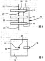
Fig. 1 represents three LED crystal spares 12,14,16 that have the flat disc moulding of band square edge profile respectively.
Each LED crystal spare is all formed by the wafer cutting of a corresponding doping batching, and it has p-doping sublayer and n-doping sublayer.Therefore at compound the obtain light of the p-n intersection that obtains like this by electronics and hole.
In order to ensure, provide from LED crystal spare 12,14,16 light that sends along any direction for use, LED crystal spare 12,14,16 totally keeps with 18 supporting arrangements of representing in this wise by one, so that its boundary face exposes basically.
LED crystal spare 12,14,16 connects by bonding conductor 20 mutually for this reason, is respectively equipped with input lead 22 and 24 at the LED of edge crystal spare 12,16 on its outside.
Be installed on a device case, the circuit board etc. in the mode that need not describe in detail at 32 supportings of U-shaped support, itself that the whole device shown in Fig. 1 is made by an insulating materials.
At the state that can work, input lead 22,24 is connected with dc source 34.
By above explanation as can be seen, has very simple frame for movement, because the power supply and the machinery that have adopted identical parts to be used for LED crystal spare keep by the light-emitting diode assembly of Fig. 1.Wherein keep described LED crystal spare 12,14,16 like this, so that its boundary face virtually completely exposes.
In pressing the embodiment of Fig. 2, the parts that illustrated with reference to Fig. 1 also have identical Reference numeral, and following no longer detailed description.
Replace support 32, adopt a housing 36 of making by glass to keep LED crystal spare 12,14,16.Housing is made by the glass material of extruding, and it has a circular exterior contour and a foursquare interior cross section.Determine the size of the square inner chamber 38 determined by housing 36 like this, promptly, make the edge contour of this inner chamber corresponding to LED crystal spare 12,14,16, thereby described crystal spare by certain angle direction orientation, promptly can not rotate with respect to the axis of the device of being determined by input lead 22,24 and bonding conductor 20 in inner chamber 38.
Therefore in embodiment, cancelled support 32, because housing 36 keeps input lead 22,24 by Fig. 2.
Said external and interior shape by housing 36 not only obtain the alignment of LED crystal spare 12,14,16 on angle, also obtain lens effect by four plano-convex cylindrical lens that formed by housing 36 simultaneously.
If do not wish this lens effect, housing also can be designed to have the sleeve of square cross section, and the housing parts that promptly is positioned at the front of LED crystal spare 12,14,16 sides is parallel plane plate, does not have imaging effect.
Fig. 4 illustrates a kind of light-emitting diode assembly that had illustrated with reference to Fig. 1.Be in pressing the embodiment of Fig. 4, the hollow minute surface that support 32 is designed to be recessed into.Therefore obtaining a kind of optical effect equally assembles the light that is sent by LED crystal spare 12,14,16 by this optical effect.
Correspond essentially to embodiment by Fig. 2 and 3 by the embodiment of Fig. 5, just housing 36 is designed to sphere. Input lead 22,24 fuses into its inside respectively equally, and a pipe joint 46 additionally is shown on housing 36, can be by this pipe joint with housing 36 inner emptyings, and can fill inert gas where necessary.Make pipe joint 46 fusings after the inner emptying of ball and after filling inert gas in case of necessity, thereby keeping the atmosphere (Millieu) of housing 36 inside constant.
In pressing the embodiment of Fig. 6, LED crystal spare 12,14,16 etc. are kept by bonding conductor 20 and input lead 22,24, and they are made by resistant to bending conducting line segment.Can realize front and back tactic LED crystal spare 12,14, the 16 identical angle that can tilt mutually like this.
Obtain light-emitting diode assembly uniform total emission characteristic in the light-emitting diode assembly plane thus.
Certainly, in the flexible program of the embodiment that presses Fig. 6, more LED crystal spare can be set also, thereby whole light-emitting diode assembly forms a circle, wherein this moment, input lead 22,24 closely was adjacent to radially extend out from circle mutually.
In pressing the embodiment of Fig. 7, housing 36 has the shape with the cylindrical box of parallel plane cover plate 41,43.Present described cover plate keeps a plurality of LED crystal spares 12,14,16 that kept by bonding conductor 20 and input lead 22,24 respectively.Therefore whole device forms one and has light source intensity distributions, that enlarge that remains unchanged basically.
In another kind of flexible program of the present invention, can realize that also other space of the unit that formed by LED crystal spare, bonding conductor and input lead arranges, for example by adopting a cube transparent shell, and in differently packing the cube housing into along x direction, y direction and z direction by the axis of each light-emitting diode assembly that will determine by bonding conductor 20 and input lead 22,24.Finally obtain a light source with good spherical intensity distributions.
In the embodiment that presses Fig. 8 and 9, supporting arrangement 18 is designed to harrow shape, in the intermediate space that LED crystal spare 12,14,16 is received between rake teeth.They can remain on here or install by glass dust (Glasfritte) or adhesive securement ground by interference fit.
The rake teeth of supporting arrangement 18 particularly has and keeps LED crystal spare 12,14,16 needed length reliably.The boundary face of crystal spare also exposes basically in by the embodiment of Fig. 8 and 9 for this reason.
Supporting arrangement 18 can be a forming of glass spare or a plastics forming spare actually, and its width is roughly 1/5th to 1/3rd of the LED crystal spare length of side.
In the flexible program of the embodiment that presses Fig. 8 and 9, the supporting structure 18 of rake shape also can be selected the shape of circular arc ring, thereby also can obtain the advantage that light intensity that light-emitting diode assembly sends distributes by even angle.
In pressing the embodiment of Figure 10 to 12, the front has identical Reference numeral in conjunction with the parts that other light-emitting diode assembly of shape of equivalence on the function had illustrated.No longer describe these parts below in detail.Feature by the form of implementation of Figure 10 to 12 is, is adjacent to be provided with specular surface body with light emitting diode, and described specular surface body has the minute surface of revolution symmetry, and the axis of minute surface aligns with the line of the tactic light emitting diode in front and back basically.
In pressing the embodiment of Figure 10, the bonding conductor 20 that extends between adjacent light emitting diode 12,14,16 is designed to have the electric conductor of the symmetrical minute surface of revolution.In pressing the embodiment of Figure 10, bonding conductor 20 has two minute surfaces 50,52 that fit mutually with its wide bottom surface, that revolution is symmetrical, and they form the part of a hyperboloid of revolution respectively.
Like this, two minute surfaces 50,52 are radially launched light basically, and described light penetrates from the end face of light emitting diode 12,14 etc.
In pressing the embodiment of Figure 10, the common-base mask of two minute surfaces 50,52 has the diameter and identical edge contour substantially the same with LED crystal spare 12,14,16, and therefore same shape is received in the inner chamber 38 of housing 36 sealedly.
The end face of hyperboloid bonding conductor 20 can be connected with the end face soldering of adjacent LED crystal spare.
But in flexible program, also can be for example by one or two spring contact whole group (Stapel) that comprises LED crystal spare 12,14,16 and be connected the hyperboloid bonding conductor 20 between them be carried out the elasticity pretension, described contact acts on described group the end and by housing 36 and keeps.
A kind of such light-emitting diode assembly shown in Figure 11.Wherein bonding conductor 22 has the semicircle spring section 22F of a clip spring, and bonding conductor 24 has a contact plate 24K.
In addition, in Figure 11, the positive contact of LED crystal spare 12,14,16 is represented with 12A, 14A, 16A, negative contact 12K, and 14K, 16K represents.
The embodiment that presses Figure 11 is similar with the embodiment that presses Figure 10 aspect all the other, (except) only be between front and back tactic LED crystal spare 12,14,16, to have the bonding conductor 20 that is designed to single paraboloid of revolution minute surface.
This device with only to the use that combines of the LED crystal spare of side emission light.In the common LED crystal spare, this crystal spare is only launched in anode region on many markets, and cathode side is the light impermeable.
In pressing the embodiment of Figure 12, the specular surface body 54 of suit hull shape on bonding conductor 20, described specular surface body have the oval shape of revolution respectively.Make the light of launching by radially inside directions such as LED crystal spares 12,14,16 turn to radially outside direction by described specular surface body 54.
The chain that specular surface body 54 also can be designed to link together.Described specular surface body also can have the rhombus minute surface shape (parabolical groove (Kannelierung)) that has the cross section that remains unchanged vertically.
Therefore the light-emitting diode assembly by Figure 12 produces a plate-like light curtain.
In another embodiment shown in Figure 13, LED crystal spare 12 is formed by complex.Described complex is connected with supporting arrangement 18 in its edge on Figure 13 the right.
LED crystal spare 12 comprises a foursquare parallel plane matrix 56, and described matrix is made by clear glass, particularly sapphire glass (Saphirglas).Matrix 56 supportings one sandwich construction, described sandwich construction has with lower floor: a p-conductive layer 58, is positioned at the mqw layer 59 and a n-conductive layer 60 of its back.First electrode layer 62 is set, and the downside of n type conductive layer is connected with 64 of the second electrode lays by the surface bearing of matrix 56 on the upside of p-conductive layer 58.
Supporting arrangement 18 comprises two connecting bands 70,72 with flat rectangular cross section, but the size of cross section is chosen to make connecting band the 70, the 72nd, from what support.Connecting band 70 is connected with electrode layer 62 by welding position 74, and connecting band 72 is connected with electrode layer 60 by welding position 76.
Described layer 58,59,60,62 and 64 thin like this, and consequently whole sandwich construction is a printing opacity, and described light is produced by the combination again in electronics in the sandwich construction 58,59,60 and hole.
By in methods shown in Figure 13, can in a simple manner a plurality of standard LED crystal spares mechanically be connected into row, its electricity is connected.
Claims (24)
1. light-emitting diode assembly, have a plurality of LED crystal spares (12,14,16), and have two respectively and be used for a LED crystal spare (12,14,16) input lead (22,24), described LED crystal spare (12,14,16) can be connected with power supply (34) by described input lead, described light emitting diode has a crystal supporting arrangement (18), this supporting arrangement supports LED crystal spare (12 in this wise, 14,16), promptly, the boundary face of described crystal spare exposes in this wise, make except the contact fixed area, light is at LED crystal spare (12,14,16) can both penetrate on all boundary faces, it is characterized by, supporting arrangement (18) is arranged on crystal spare (12) edge.
2. by the light-emitting diode assembly of claim 1, it is characterized by: supporting arrangement (18) comprises the input lead (22,24) that is designed to cable sections, wire segments or thin bar.
3. by claim 1 or 2 light-emitting diode assembly, it is characterized by: supporting arrangement (18) is the coefficient rigid body in neighboring with LED crystal spare (12,14,16).
4. by the light-emitting diode assembly of claim 3, it is characterized by: described rigid body has the design of rake shape, and this rake shape design has short tooth.
5. by the light-emitting diode assembly of claim 1 or 2, it is characterized by: supporting arrangement (18) is by regular to each other spacing supporting LED crystal spare (12,14,16).
6. by the light-emitting diode assembly of claim 1 or 2, it is characterized by: supporting arrangement (18) is with substantially parallel layout supporting LED crystal spare (12,14,16).
7. by claim 1 or 2 light-emitting diode assembly, it is characterized by: supporting arrangement (18) is at front and back tactic LED crystal spare (12,14,16) the situation lower support LED crystal spare (12,14,16) of relative tilt similarly.
8. by the light-emitting diode assembly of claim 1 or 2, it is characterized by: LED crystal spare (12,14,16) and supporting arrangement (18) are arranged in the transparent housing (36).
9. by the light-emitting diode assembly of claim 8, it is characterized by: housing (36) is pumped into vacuum.
10. by the light-emitting diode assembly of claim 8, it is characterized by: fill housing (36) with inert gas.
11. the light-emitting diode assembly by claim 8 is characterized by: the inner chamber (38) of housing (36) is complementary with the exterior contour of LED crystal spare (12,14,16).
12. by the light-emitting diode assembly of claim 8, it is characterized by: housing (36) is made by flint glass or colourless plastic material.
13. by the light-emitting diode assembly of claim 1 or 2, it is characterized by: LED crystal spare is arranged on the Optical devices back of scattering, or is arranged on the Optical devices front of reflection.
14. the light-emitting diode assembly by claim 1 or 2 is characterized by: near LED crystal spare (12,14,16) minute surface (50,52 is set; 54).
15. the light-emitting diode assembly by claim 14 is characterized by: minute surface (50,52; 54) be the surface of revolution.
16. by the light-emitting diode assembly of claim 15, it is characterized by: minute surface is hyperboloid of revolution, paraboloid of revolution or spheroid.
17. the light-emitting diode assembly by claim 14 is characterized by: minute surface (50,52; 54) axis aligns with the line of front and back tactic LED crystal spare (12,14,16) basically.
18. each light-emitting diode assembly by claim 14, it is characterized by: the edge contour that is designed to minute surface (50,52) of bonding conductor (20) is corresponding with the edge contour of LED crystal spare (12,14,16), and minute surface (50,52) shape is positioned in the housing (36) of admitting LED crystal spare (12,14,16) sealedly.
19. light-emitting diode assembly by claim 1, it is characterized by: supporting arrangement (18) comprises two input leads (70,74), draw by the edge of crystal spare (12) on described input lead insulation ground, and be connected with two electrodes (62,64) of crystal spare (12) respectively.
20. by the light-emitting diode assembly of claim 19, it is characterized by: described input lead has rectangular cross section.
21. by the light-emitting diode assembly of claim 1 or 2, it is characterized by: crystal spare (12) has the matrix (56) of insulation, described matrix comprises p-conductive layer (58), n-conductive layer (60) and the electrode of connecting with described layer (62,64).
22. the light-emitting diode assembly by claim 21 is characterized by: between p-conductive layer (58) and n-conductive layer (60) MQW-layer (59) is set.
23., it is characterized by by the light-emitting diode assembly of claim 21: insulating body (56) and by the layer (58,59,60,62,64) of described substrate support for emitted light at least the part be permeable.
24., it is characterized by by the light-emitting diode assembly of claim 23: insulating body (56) and by the layer (58,59,60,62,64) of described substrate support for emitted only permeable fully.
Applications Claiming Priority (2)
| Application Number | Priority Date | Filing Date | Title |
|---|---|---|---|
| DE102005024830A DE102005024830B4 (en) | 2005-05-27 | 2005-05-27 | Light emitting diode array |
| DE102005024830.6 | 2005-05-27 |
Publications (2)
| Publication Number | Publication Date |
|---|---|
| CN1873314A CN1873314A (en) | 2006-12-06 |
| CN1873314B true CN1873314B (en) | 2011-04-13 |
Family
ID=36791596
Family Applications (1)
| Application Number | Title | Priority Date | Filing Date |
|---|---|---|---|
| CN2006100846735A Expired - Fee Related CN1873314B (en) | 2005-05-27 | 2006-05-29 | Light-emitting diode arrangement |
Country Status (5)
| Country | Link |
|---|---|
| US (1) | US7872275B2 (en) |
| EP (1) | EP1727202A3 (en) |
| CN (1) | CN1873314B (en) |
| DE (1) | DE102005024830B4 (en) |
| HK (1) | HK1100495A1 (en) |
Families Citing this family (7)
| Publication number | Priority date | Publication date | Assignee | Title |
|---|---|---|---|---|
| US7943953B2 (en) * | 2006-01-31 | 2011-05-17 | Kyocera Corporation | Light emitting device and light emitting module |
| WO2008073400A1 (en) | 2006-12-11 | 2008-06-19 | The Regents Of The University Of California | Transparent light emitting diodes |
| DE102008048650A1 (en) * | 2008-09-24 | 2010-04-01 | Osram Opto Semiconductors Gmbh | Radiation emitting device |
| SG185159A1 (en) * | 2011-04-26 | 2012-11-29 | Novalite Technology Pte Ltd | Gas cooled light emitting diodes |
| DE102016113206A1 (en) * | 2016-07-18 | 2018-01-18 | Osram Opto Semiconductors Gmbh | Radiation emitting device |
| US11592166B2 (en) | 2020-05-12 | 2023-02-28 | Feit Electric Company, Inc. | Light emitting device having improved illumination and manufacturing flexibility |
| US11876042B2 (en) | 2020-08-03 | 2024-01-16 | Feit Electric Company, Inc. | Omnidirectional flexible light emitting device |
Citations (3)
| Publication number | Priority date | Publication date | Assignee | Title |
|---|---|---|---|---|
| DE2920444A1 (en) * | 1978-05-24 | 1979-12-06 | Western Electric Co | SEMICONDUCTOR COMPONENT AND METHOD FOR ITS PRODUCTION |
| EP1213773A1 (en) * | 1999-07-26 | 2002-06-12 | Labosphere Institute | Bulk lens, light emitting body, lighting device and optical information system |
| US6455878B1 (en) * | 2001-05-15 | 2002-09-24 | Lumileds Lighting U.S., Llc | Semiconductor LED flip-chip having low refractive index underfill |
Family Cites Families (8)
| Publication number | Priority date | Publication date | Assignee | Title |
|---|---|---|---|---|
| US3588636A (en) * | 1969-01-27 | 1971-06-28 | Globe Union Inc | Ohmic contact and method and composition for forming same |
| FR2658344B1 (en) * | 1990-02-09 | 1994-09-23 | Neiman Sa | REMOTE CONTROL SYSTEM, PARTICULARLY FOR LOCKING / UNLOCKING DOORS FOR MOTOR VEHICLES. |
| US6294800B1 (en) * | 1998-02-06 | 2001-09-25 | General Electric Company | Phosphors for white light generation from UV emitting diodes |
| EP1113506A3 (en) * | 1999-12-28 | 2005-03-16 | Toyoda Gosei Co., Ltd. | Light emitting diode |
| JP3915873B2 (en) * | 2000-11-10 | 2007-05-16 | セイコーエプソン株式会社 | Manufacturing method of optical device |
| US7380961B2 (en) * | 2002-04-24 | 2008-06-03 | Moriyama Sangyo Kabushiki Kaisha | Light source coupler, illuminant device, patterned conductor, and method for manufacturing light source coupler |
| US20050068777A1 (en) | 2003-09-25 | 2005-03-31 | Dragoslav Popovic | Modular LED light and method |
| DE102005050947A1 (en) * | 2005-10-22 | 2007-04-26 | Noctron S.A.R.L. | Luminous element with at least one luminescent chip crystal |
-
2005
- 2005-05-27 DE DE102005024830A patent/DE102005024830B4/en not_active Expired - Fee Related
-
2006
- 2006-05-05 EP EP06009282A patent/EP1727202A3/en not_active Withdrawn
- 2006-05-26 US US11/442,672 patent/US7872275B2/en not_active Expired - Fee Related
- 2006-05-29 CN CN2006100846735A patent/CN1873314B/en not_active Expired - Fee Related
-
2007
- 2007-05-29 HK HK07105686.1A patent/HK1100495A1/en not_active IP Right Cessation
Patent Citations (3)
| Publication number | Priority date | Publication date | Assignee | Title |
|---|---|---|---|---|
| DE2920444A1 (en) * | 1978-05-24 | 1979-12-06 | Western Electric Co | SEMICONDUCTOR COMPONENT AND METHOD FOR ITS PRODUCTION |
| EP1213773A1 (en) * | 1999-07-26 | 2002-06-12 | Labosphere Institute | Bulk lens, light emitting body, lighting device and optical information system |
| US6455878B1 (en) * | 2001-05-15 | 2002-09-24 | Lumileds Lighting U.S., Llc | Semiconductor LED flip-chip having low refractive index underfill |
Also Published As
| Publication number | Publication date |
|---|---|
| HK1100495A1 (en) | 2007-09-21 |
| US20060267032A1 (en) | 2006-11-30 |
| US7872275B2 (en) | 2011-01-18 |
| DE102005024830A1 (en) | 2006-12-07 |
| DE102005024830B4 (en) | 2009-07-02 |
| CN1873314A (en) | 2006-12-06 |
| EP1727202A2 (en) | 2006-11-29 |
| EP1727202A3 (en) | 2008-07-02 |
Similar Documents
| Publication | Publication Date | Title |
|---|---|---|
| CN1873314B (en) | Light-emitting diode arrangement | |
| US9146026B2 (en) | Lighting device including light-emitting element and method for manufacturing the same | |
| US20100046220A1 (en) | Led unit and led lighting lamp using the led unit | |
| US20080239716A1 (en) | Light strip | |
| EP2650590A2 (en) | Light emitting package | |
| US9599289B2 (en) | Light source and lighting device including the same | |
| CN104126096A (en) | Heat-dissipating structure for lighting apparatus and lighting apparatus | |
| US10670194B2 (en) | SSL lamp that includes three or more crossed elongated light emitting structures | |
| EP2860775A1 (en) | Light emitting diode package | |
| KR20170131910A (en) | light emitting device and lighting bulb comprising the same | |
| US20130106279A1 (en) | Light-Emitting Module and Luminaire | |
| JP2006324036A (en) | Led bulb for vehicular lamp | |
| US20130201669A1 (en) | Led illumination apparatus with improved output uniformity | |
| EP3963252B1 (en) | Led filament lamp | |
| JP5952557B2 (en) | Light emitting module and vehicle lamp | |
| US11346508B2 (en) | LED filament | |
| JP2015015110A (en) | Light emitting module and lighting system | |
| KR100900400B1 (en) | Light emitting device with aspherical lens and back light unit comprising the same | |
| US7989837B2 (en) | Light chain | |
| KR20170119503A (en) | light emitting device and light emitting bulb comprising the same | |
| US20110042709A1 (en) | Free-standing mounted light emitting diodes for general lighting | |
| US20180245758A1 (en) | Light source module, illumination device and moving body | |
| US11933459B2 (en) | Lamp including reduced phosphor light emitting diode filaments | |
| JP2012054104A (en) | Circular lighting system | |
| JP5305708B2 (en) | Light emitting device |
Legal Events
| Date | Code | Title | Description |
|---|---|---|---|
| C06 | Publication | ||
| PB01 | Publication | ||
| REG | Reference to a national code |
Ref country code: HK Ref legal event code: DE Ref document number: 1100495 Country of ref document: HK |
|
| C10 | Entry into substantive examination | ||
| SE01 | Entry into force of request for substantive examination | ||
| C14 | Grant of patent or utility model | ||
| GR01 | Patent grant | ||
| REG | Reference to a national code |
Ref country code: HK Ref legal event code: GR Ref document number: 1100495 Country of ref document: HK |
|
| C17 | Cessation of patent right | ||
| CF01 | Termination of patent right due to non-payment of annual fee |
Granted publication date: 20110413 Termination date: 20140529 |