DE112009001143T5 - Active matrix displays - Google Patents
Active matrix displays Download PDFInfo
- Publication number
- DE112009001143T5 DE112009001143T5 DE112009001143T DE112009001143T DE112009001143T5 DE 112009001143 T5 DE112009001143 T5 DE 112009001143T5 DE 112009001143 T DE112009001143 T DE 112009001143T DE 112009001143 T DE112009001143 T DE 112009001143T DE 112009001143 T5 DE112009001143 T5 DE 112009001143T5
- Authority
- DE
- Germany
- Prior art keywords
- circuit
- active matrix
- programmable
- drive
- oled display
- Prior art date
- Legal status (The legal status is an assumption and is not a legal conclusion. Google has not performed a legal analysis and makes no representation as to the accuracy of the status listed.)
- Withdrawn
Links
Images


Classifications
-
- G—PHYSICS
- G09—EDUCATION; CRYPTOGRAPHY; DISPLAY; ADVERTISING; SEALS
- G09G—ARRANGEMENTS OR CIRCUITS FOR CONTROL OF INDICATING DEVICES USING STATIC MEANS TO PRESENT VARIABLE INFORMATION
- G09G3/00—Control arrangements or circuits, of interest only in connection with visual indicators other than cathode-ray tubes
- G09G3/20—Control arrangements or circuits, of interest only in connection with visual indicators other than cathode-ray tubes for presentation of an assembly of a number of characters, e.g. a page, by composing the assembly by combination of individual elements arranged in a matrix no fixed position being assigned to or needed to be assigned to the individual characters or partial characters
- G09G3/22—Control arrangements or circuits, of interest only in connection with visual indicators other than cathode-ray tubes for presentation of an assembly of a number of characters, e.g. a page, by composing the assembly by combination of individual elements arranged in a matrix no fixed position being assigned to or needed to be assigned to the individual characters or partial characters using controlled light sources
- G09G3/30—Control arrangements or circuits, of interest only in connection with visual indicators other than cathode-ray tubes for presentation of an assembly of a number of characters, e.g. a page, by composing the assembly by combination of individual elements arranged in a matrix no fixed position being assigned to or needed to be assigned to the individual characters or partial characters using controlled light sources using electroluminescent panels
- G09G3/32—Control arrangements or circuits, of interest only in connection with visual indicators other than cathode-ray tubes for presentation of an assembly of a number of characters, e.g. a page, by composing the assembly by combination of individual elements arranged in a matrix no fixed position being assigned to or needed to be assigned to the individual characters or partial characters using controlled light sources using electroluminescent panels semiconductive, e.g. using light-emitting diodes [LED]
- G09G3/3208—Control arrangements or circuits, of interest only in connection with visual indicators other than cathode-ray tubes for presentation of an assembly of a number of characters, e.g. a page, by composing the assembly by combination of individual elements arranged in a matrix no fixed position being assigned to or needed to be assigned to the individual characters or partial characters using controlled light sources using electroluminescent panels semiconductive, e.g. using light-emitting diodes [LED] organic, e.g. using organic light-emitting diodes [OLED]
- G09G3/3275—Details of drivers for data electrodes
- G09G3/3283—Details of drivers for data electrodes in which the data driver supplies a variable data current for setting the current through, or the voltage across, the light-emitting elements
-
- G—PHYSICS
- G09—EDUCATION; CRYPTOGRAPHY; DISPLAY; ADVERTISING; SEALS
- G09G—ARRANGEMENTS OR CIRCUITS FOR CONTROL OF INDICATING DEVICES USING STATIC MEANS TO PRESENT VARIABLE INFORMATION
- G09G3/00—Control arrangements or circuits, of interest only in connection with visual indicators other than cathode-ray tubes
- G09G3/20—Control arrangements or circuits, of interest only in connection with visual indicators other than cathode-ray tubes for presentation of an assembly of a number of characters, e.g. a page, by composing the assembly by combination of individual elements arranged in a matrix no fixed position being assigned to or needed to be assigned to the individual characters or partial characters
- G09G3/22—Control arrangements or circuits, of interest only in connection with visual indicators other than cathode-ray tubes for presentation of an assembly of a number of characters, e.g. a page, by composing the assembly by combination of individual elements arranged in a matrix no fixed position being assigned to or needed to be assigned to the individual characters or partial characters using controlled light sources
- G09G3/30—Control arrangements or circuits, of interest only in connection with visual indicators other than cathode-ray tubes for presentation of an assembly of a number of characters, e.g. a page, by composing the assembly by combination of individual elements arranged in a matrix no fixed position being assigned to or needed to be assigned to the individual characters or partial characters using controlled light sources using electroluminescent panels
- G09G3/32—Control arrangements or circuits, of interest only in connection with visual indicators other than cathode-ray tubes for presentation of an assembly of a number of characters, e.g. a page, by composing the assembly by combination of individual elements arranged in a matrix no fixed position being assigned to or needed to be assigned to the individual characters or partial characters using controlled light sources using electroluminescent panels semiconductive, e.g. using light-emitting diodes [LED]
- G09G3/3208—Control arrangements or circuits, of interest only in connection with visual indicators other than cathode-ray tubes for presentation of an assembly of a number of characters, e.g. a page, by composing the assembly by combination of individual elements arranged in a matrix no fixed position being assigned to or needed to be assigned to the individual characters or partial characters using controlled light sources using electroluminescent panels semiconductive, e.g. using light-emitting diodes [LED] organic, e.g. using organic light-emitting diodes [OLED]
- G09G3/3225—Control arrangements or circuits, of interest only in connection with visual indicators other than cathode-ray tubes for presentation of an assembly of a number of characters, e.g. a page, by composing the assembly by combination of individual elements arranged in a matrix no fixed position being assigned to or needed to be assigned to the individual characters or partial characters using controlled light sources using electroluminescent panels semiconductive, e.g. using light-emitting diodes [LED] organic, e.g. using organic light-emitting diodes [OLED] using an active matrix
- G09G3/3233—Control arrangements or circuits, of interest only in connection with visual indicators other than cathode-ray tubes for presentation of an assembly of a number of characters, e.g. a page, by composing the assembly by combination of individual elements arranged in a matrix no fixed position being assigned to or needed to be assigned to the individual characters or partial characters using controlled light sources using electroluminescent panels semiconductive, e.g. using light-emitting diodes [LED] organic, e.g. using organic light-emitting diodes [OLED] using an active matrix with pixel circuitry controlling the current through the light-emitting element
-
- H—ELECTRICITY
- H10—SEMICONDUCTOR DEVICES; ELECTRIC SOLID-STATE DEVICES NOT OTHERWISE PROVIDED FOR
- H10K—ORGANIC ELECTRIC SOLID-STATE DEVICES
- H10K50/00—Organic light-emitting devices
- H10K50/10—OLEDs or polymer light-emitting diodes [PLED]
- H10K50/11—OLEDs or polymer light-emitting diodes [PLED] characterised by the electroluminescent [EL] layers
-
- H—ELECTRICITY
- H10—SEMICONDUCTOR DEVICES; ELECTRIC SOLID-STATE DEVICES NOT OTHERWISE PROVIDED FOR
- H10K—ORGANIC ELECTRIC SOLID-STATE DEVICES
- H10K59/00—Integrated devices, or assemblies of multiple devices, comprising at least one organic light-emitting element covered by group H10K50/00
-
- H—ELECTRICITY
- H10—SEMICONDUCTOR DEVICES; ELECTRIC SOLID-STATE DEVICES NOT OTHERWISE PROVIDED FOR
- H10K—ORGANIC ELECTRIC SOLID-STATE DEVICES
- H10K59/00—Integrated devices, or assemblies of multiple devices, comprising at least one organic light-emitting element covered by group H10K50/00
- H10K59/10—OLED displays
- H10K59/12—Active-matrix OLED [AMOLED] displays
-
- G—PHYSICS
- G09—EDUCATION; CRYPTOGRAPHY; DISPLAY; ADVERTISING; SEALS
- G09G—ARRANGEMENTS OR CIRCUITS FOR CONTROL OF INDICATING DEVICES USING STATIC MEANS TO PRESENT VARIABLE INFORMATION
- G09G2300/00—Aspects of the constitution of display devices
- G09G2300/04—Structural and physical details of display devices
- G09G2300/0404—Matrix technologies
- G09G2300/0408—Integration of the drivers onto the display substrate
-
- G—PHYSICS
- G09—EDUCATION; CRYPTOGRAPHY; DISPLAY; ADVERTISING; SEALS
- G09G—ARRANGEMENTS OR CIRCUITS FOR CONTROL OF INDICATING DEVICES USING STATIC MEANS TO PRESENT VARIABLE INFORMATION
- G09G2310/00—Command of the display device
- G09G2310/02—Addressing, scanning or driving the display screen or processing steps related thereto
- G09G2310/0243—Details of the generation of driving signals
- G09G2310/0248—Precharge or discharge of column electrodes before or after applying exact column voltages
-
- G—PHYSICS
- G09—EDUCATION; CRYPTOGRAPHY; DISPLAY; ADVERTISING; SEALS
- G09G—ARRANGEMENTS OR CIRCUITS FOR CONTROL OF INDICATING DEVICES USING STATIC MEANS TO PRESENT VARIABLE INFORMATION
- G09G2310/00—Command of the display device
- G09G2310/02—Addressing, scanning or driving the display screen or processing steps related thereto
- G09G2310/0262—The addressing of the pixel, in a display other than an active matrix LCD, involving the control of two or more scan electrodes or two or more data electrodes, e.g. pixel voltage dependent on signals of two data electrodes
-
- G—PHYSICS
- G09—EDUCATION; CRYPTOGRAPHY; DISPLAY; ADVERTISING; SEALS
- G09G—ARRANGEMENTS OR CIRCUITS FOR CONTROL OF INDICATING DEVICES USING STATIC MEANS TO PRESENT VARIABLE INFORMATION
- G09G2320/00—Control of display operating conditions
- G09G2320/02—Improving the quality of display appearance
- G09G2320/0223—Compensation for problems related to R-C delay and attenuation in electrodes of matrix panels, e.g. in gate electrodes or on-substrate video signal electrodes
Abstract
Aktivmatrix-OLED-Anzeige, die eine Datenleitung, mehrere Pixelschaltungen, die mit der Datenleitung verbunden sind, eine Ansteuerungsschaltung, die in der Umgebung eines Endes der Datenleitung angeschlossen ist, um Anzeigedaten in Pixelschaltungen zu schreiben, und eine programmierbare Ansteuerungsverstärkungsschaltung, die in der Umgebung eines weiteren Endes der Datenleitung gegenüber der Ansteuerungsschaltung angeschlossen ist, umfasst.An active matrix OLED display comprising a data line, a plurality of pixel circuits connected to the data line, a drive circuit connected in the vicinity of one end of the data line to write display data in pixel circuits, and a programmable drive amplification circuit in the environment another end of the data line is connected to the drive circuit.

Description
Diese Erfindung bezieht sich im Allgemeinen auf Aktivmatrixanzeigen und auf darauf bezogene Anzeigeansteuerungsverfahren. Insbesondere bezieht sich die Erfindung auf eine zusätzliche Ansteuerungsschaltungsanordnung für Aktivmatrixanzeigen mit angesteuerten organischen Leuchtdioden (OLED), die verwendet werden, um die Leistungscharakteristik der Vorrichtung zu verbessern.This invention relates generally to active matrix displays and related display control methods. In particular, the invention relates to additional drive circuitry for activated matrix organic light emitting diode (OLED) displays used to enhance the performance of the device.
Anzeigen, die unter Verwendung von OLEDs gefertigt werden, bieten gegenüber LCD- und anderen Flachbildschirm-Technologien zahlreiche Vorteile. Sie sind hell, farbenfreudig, schnell schaltend (im Vergleich zu LCDs), sie schaffen einen weiten Betrachtungswinkel und sie sind einfach und kostengünstig auf vielen verschieden Substraten herzustellen. Organische LEDs (die hier organometallische LEDs umfassen) können unter Verwendung von Materialien einschließlich Polymeren, kleinen Molekülen und Dendrimeren in einem Bereich von Farben, die von den verwendeten Materialien abhängen, gefertigt werden. Beispiele organischer LEDs auf Polymerbasis sind beschrieben in
Eine typische OLED-Vorrichtung umfasst zwei Schichten aus organischem Material, wovon eine eine Schicht aus lichtemittierendem Material wie etwa ein lichtemittierendes Polymer (LEP), aus einem Oligomer oder aus einem lichtemittierenden Material mit niedrigem Molekulargewicht ist und die andere eine Schicht aus einem Lochtransportmaterial wie etwa ein Polythiophen-Derivat oder ein Polyanlilin-Derivat ist.A typical OLED device comprises two layers of organic material, one of which is a layer of light emitting material such as a light emitting polymer (LEP), an oligomer or a low molecular weight light emitting material and the other is a layer of a hole transporting material such as a polythiophene derivative or a polyaniline derivative.
Organische LEDs können auf einem Substrat in einer Matrix aus Pixeln abgelagert sein, um eine einfarbige oder mehrfarbige Pixelanzeige zu bilden. Eine mehrfarbige Anzeige kann unter Verwendung von Gruppen aus rot, grün und blau emittierenden Pixeln konstruiert sein. So genannte Aktivmatrixanzeigen (AM-Anzeigen) besitzen ein Speicherelement, typischerweise einen Speicherkondensator und einen Transistor, die jedem Pixel zugeordnet sind, während Passivmatrixanzeigen kein solches Speicherelement besitzen und stattdessen wiederholt abgetastet werden, um den Eindruck eines dauerhaften Bildes zu geben. Beispiele von Treibern für Aktivmatrixanzeigen aus Polymer oder kleinen Molekülen finden sich in
Eine Anzeige kann entweder an der Unterseite emittieren (Bottom-Emitter) oder an der Oberseite emittieren (Top-Emitter). In einer Anzeige, die an der Unterseite emittiert, wird Licht durch das Substrat, auf dem die Aktivmatrixschaltungsanordnung gefertigt ist, emittiert; in einer Anzeige, die an der Oberseite emittiert, wird Licht ohne Durchgang durch eine Schicht der Anzeige, in der die Aktivmatrixschaltungsanordnung gefertigt ist, zu einer vorderen Fläche der Anzeige emittiert.An indicator can either emit at the bottom (bottom emitter) or emit at the top (top emitter). In a display emitting at the bottom, light is emitted through the substrate on which the active matrix circuitry is fabricated; in a display emitting at the top, light is emitted to a front surface of the display without passing through a layer of the display in which the active matrix circuitry is fabricated.
OLED-Anzeigen mit Oberseitenemission sind weniger verbreitet als Anzeigen mit Unterseitenemission, weil typischerweise die obere Elektrode die Katode enthält, die wenigstens teilweise lichtdurchlässig sein muss und außerdem eine ausreichende spezifische elektrische Leitfähigkeit besitzen muss und vorzugsweise eine gewisse Einkapselung der darunterliegenden organischen Schichten schafft. Dennoch sind viele verschiedene Strukturen mit Oberseitenemission beschrieben worden, einschließlich der veröffentlichten PCT-Anmeldung
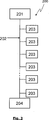
Eine OLED-Anzeige zeigt herkömmlicherweise ein Bild an, das aus einer rechtwinkligen Matrix aus Bildelementen (oder Pixeln) aufgebaut ist. Eine Aktivmatrix-OLED-Anzeige besitzt herkömmlicherweise für jede Farbe jedes Pixels eine Zeilendatenleitung und eine Spaltendatenleitung. Eine solche Datenleitung
In einer Aktivmatrix-OLED-Anzeige verwenden Datenleitungen
Ein Problem, das mittels Strom angesteuerten Aktivmatrix-Pixelschaltungen gemeinsam ist, besteht darin, dass dort, wo die Pixel-”Programmierungs”-Ströme klein sind, was oft der Fall ist, ein Stromleck und/oder eine Datenleitungskapazität vorherrschen, insbesondere bei großen Anzeigen.A problem common to current driven active matrix pixel circuits is that where the pixel "programming" currents are small, as is often the case, there is a current leak and / or data line capacitance, especially with large displays ,
Wie am besten in
Gemäß einem ersten Aspekt der vorliegenden Erfindung wird eine Aktivmatrix-OLED-Anzeige geschaffen, die eine Datenleitung, mehrere Pixelschaltungen, die mit der Datenleitung verbunden sind, eine Ansteuerungsschaltung, die in der Umgebung eines Endes der Datenleitung angeschlossen ist, um Anzeigedaten in die Pixelschaltungen zu schreiben, und eine programmierbare Ansteuerungsverstärkungsschaltung, die in der Umgebung des anderen Endes der Datenleitung gegenüber der Ansteuerungsschaltung angeschlossen ist, umfasst.According to a first aspect of the present invention, there is provided an active matrix OLED display comprising a data line, a plurality of pixel circuits connected to the data line, a drive circuit connected in the vicinity of one end of the data line, display data in the pixel circuits and a programmable drive amplification circuit connected in the vicinity of the other end of the data line opposite to the drive circuit.
Die Erfindung schafft vorzugsweise eine programmierbare Ansteuerungsverstärkungsschaltung, die an die Datenleitung an einem Ende angeschlossen ist, das dem Ende gegenüberliegt, an dem die Ansteuerungsschaltung angeschlossen ist. Die Hinzufügung einer solchen Schaltung ermöglicht ein schnelleres Vorladen der Aktivmatrix-OLED-Datenleitung. Wie der Fachmann auf dem Gebiet erkennt, kann die programmierbare Ansteuerungsverstärkungsschaltung eine spannungsgesteuerte Schaltung oder eine stromgesteuerte Schaltung sein.The invention preferably provides a programmable drive boost circuit connected to the data line at an end opposite the end to which the drive circuit is connected. The addition of such a circuit allows faster precharging of the active matrix OLED data line. As those skilled in the art will appreciate, the programmable drive boost circuit may be a voltage controlled or current controlled circuit.
Vorzugsweise ist die programmierbare Ansteuerungsverstärkungsschaltung eine Stromquelle oder eine Stromsenke. Die Verwendung der programmierbaren Ansteuerungsverstärkungsschaltung als eine Stromquelle oder eine Stromsenke reduziert den Strom, der erforderlich ist, um den Widerstands-Kondensator-Koeffizienten der Datenleitung zu überwinden. Der Nutzen der vorliegenden Erfindung umfasst einen erhöhten Vorrichtungsleistungswirkungsgrad und eine kürzere Zeit zum Anzeigen eines Bildes und folglich höhere Bildanzeige-Auffrischungsraten.Preferably, the programmable drive boost circuit is a current source or a current sink. The use of the programmable drive boost circuit as a current source or current sink reduces the current required to overcome the data line resistance-to-capacitor coefficient. The benefit of the present invention includes increased device performance and a shorter time to display an image and, consequently, higher image refresh rates.
Vorzugsweise umfasst die programmierbare Ansteuerungsverstärkungsschaltung eine Auswahl oder Freigabeschaltung. Stärker bevorzugt ist die Ansteuerungsschaltung mit der Freigabeschaltung durch einen Datenbus verbunden. Dies ermöglicht der Ansteuerungsschaltung, die programmierbare Ansteuerungsverstärkungsschaltung durch Senden eines Freigabedatenbits und/oder eines oder mehrerer Programmdatenbits zu steuern.Preferably, the programmable drive boost circuit comprises a select or enable circuit. More preferably, the drive circuit is connected to the enable circuit through a data bus. This allows the drive circuit to control the programmable drive boost circuit by transmitting a grant data bit and / or one or more program data bits.
Vorzugsweise ist die programmierbare Ansteuerungsverstärkungsschaltung ein Stromkopierer. Optional kann der Stromkopierer als eine variable Stromsenke mit einem durch den Tastgrad programmierten Freigabesignal oder durch ein höchstwertiges Bit eines programmierten Datensignals gesteuert werden oder kann der Kopierer für eine feste Zeitdauer freigegeben werden. Die programmierbare Ansteuerungsverstärkungsschaltung kann in Abhängigkeit von Schaltungsentwurfsanforderungen vom n-Kanal-Typ oder vom p-Kanal-Typ sein.Preferably, the programmable drive boost circuit is a power copier. Optionally, the stream copier may be controlled as a variable current sink having a duty cycle programmed enable signal, or a most significant bit of a programmed data signal, or the copier may be enabled for a fixed amount of time. The programmable drive boost circuit may be of the n-channel type or the p-channel type depending on circuit design requirements.
Vorzugsweise befinden sich die programmierbare Ansteuerungsverstärkungsschaltung und die Ansteuerungsschaltung auf demselben Substrat. Ein geeignetes Substrat oder eine Rückwand kann aus amorphem Silicium (a-Si) gefertigt sein.Preferably, the programmable drive boost circuit and the drive circuit are on the same substrate. A suitable substrate or backplane may be made of amorphous silicon (a-Si).
Gemäß einem zweiten Aspekt der vorliegenden Erfindung wird ein Verfahren zum Programmieren einer Aktivmatrix-OLED-Anzeige geschaffen, wobei die OLED-Anzeige eine stromprogrammierte Datenleitung, mehrere Pixelschaltungen, die mit der Datenleitung verbunden sind, eine Ansteuerungsschaltung, die in der Umgebung eines Endes der Datenleitung angeschlossen ist, um Anzeigedaten in die Pixelschaltungen zu schreiben, und eine programmierbare Ansteuerungsverstärkungsschaltung, die in der Umgebung eines weiteren Endes der Datenleitung gegenüber der Ansteuerungsschaltung angeschlossen ist, umfasst; das Verfahren umfasst eine erste Adressierungsperiode, die das Programmieren der programmierbaren Ansteuerungsverstärkungsschaltung mit einem ersten Strom enthält; und eine zweite Adressierungsperiode, die das Schreiben von Anzeigedaten in die Pixel und das Zuführen des ersten Stroms zu der Datenleitung enthält.According to a second aspect of the present invention, there is provided a method of programming an active matrix OLED display, wherein the OLED display comprises a stream programmed data line, a plurality of pixel circuits connected to the data line, a drive circuit located in the vicinity of one end of the data line is connected to write display data in the pixel circuits, and a programmable drive amplification circuit which is connected in the vicinity of another end of the data line with respect to the drive circuit comprises; the method includes a first addressing period including programming the programmable drive amplification circuit with a first current; and a second addressing period including writing display data to the pixels and supplying the first stream to the data line.
Auf diese Weise wird ein Strom in der Datenleitung durch die programmierbare Verstärkerschaltung programmiert. Dieses Verfahren reduziert die Ladezeit wesentlich, außerdem reduziert das Laden der Datenleitung von beiden Enden die Widerstands-Kondensator-Konstante um etwa 75%.In this way, a current in the data line is programmed by the programmable amplifier circuit. This method significantly reduces the loading time and also reduces loading the data line from both ends the resistor-capacitor constant by about 75%.
Vorzugsweise umfasst das Programmierungsverfahren in der ersten Adressierungsperiode das Aktivieren der programmierbaren Ansteuerungsverstärkungsschaltung mit einem Freigabedatenbit und einem oder mehreren Programmdatenbits, um einen Strom bereitzustellen, der in Bezug auf den Strom, der für die Datenleitung von der Ansteuerungsschaltung bereitgestellt wird, vorgespannt ist.Preferably, in the first addressing period, the programming method comprises activating the programmable drive boost circuit with a release data bit and one or more program data bits to provide a current biased relative to the current provided to the data line by the drive circuit.
Vorzugsweise umfasst die erste Adressierungsperiode die Freigabe der programmierbaren Ansteuerungsverstärkungsschaltung für eine feste Zeitdauer.Preferably, the first addressing period comprises the enabling of the programmable drive boost circuit for a fixed period of time.
Eine solche Anordnung schafft den Nutzen der programmierbaren Verstärkerschaltung, während die Ineffizienz der ununterbrochenen Verwendung der programmierbaren Verstärkerschaltung vermieden wird.Such an arrangement provides the benefit of the programmable amplifier circuit while avoiding the inefficiency of uninterrupted use of the programmable amplifier circuit.
Vorzugsweise umfasst die erste Adressierungsperiode die Freigabe der programmierbaren Ansteuerungsverstärkungsschaltung und die Bereitstellung eines Stroms, der dem höchstwertigen Bit der digitalen Signalinformationen, die von der Treiberschaltung gesendet werden, entspricht. In einer solchen Anordnung wird der maximale Strom, der durch die programmierbare Verstärkerschaltung und die Ansteuerungsschaltungen bereitgestellt wird, reduziert.Preferably, the first addressing period comprises enabling the programmable drive boost circuit and providing a current corresponding to the most significant bit of the digital signal information sent from the driver circuit. In such an arrangement, the maximum current provided by the programmable amplifier circuit and the driving circuits is reduced.
Außerdem umfasst die erste Adressierungsperiode vorzugsweise die Programmierung der programmierbaren Verstärkerschaltung in der Weise, dass sie sich in Übereinstimmung mit einem Tastgrad verändert. In einer solchen Anordnung kann der Tastgrad beispielsweise so gewählt werden, dass physikalische Verunreinigungen im Material der Datenleitung überwunden werden, dass eine optimale Anzeigezeit oder ein optimaler elektrischer Wirkungsgrad beispielsweise in Abhängigkeit von dem Informationsgehalt des anzuzeigenden Bildes erzielt wird oder dass einem festen Tastgrad gefolgt wird, um beispielsweise die numerischen Berechnungen minimal zu machen, die erforderlich sind, um die gewünschte Bildanzeige zu erzielen.In addition, the first addressing period preferably includes programming the programmable amplifier circuit to change in accordance with a duty cycle. For example, in such an arrangement, the duty cycle may be selected to overcome physical contaminants in the data line material, to achieve optimum display time or optimum electrical efficiency, for example, depending on the information content of the image to be displayed, or to follow a fixed duty cycle. for example, to minimize the numerical calculations required to achieve the desired image display.
Nun werden Ausführungsformen der vorliegenden Erfindung lediglich beispielhaft und mit Bezug auf die beigefügten Zeichnungen weiter beschrieben, in denen:Embodiments of the present invention will now be further described, by way of example only and with reference to the accompanying drawings, in which:
Gemäß
Die Programmierung der Anzeige
Die programmierbare Ansteuerungsverstärkerschaltung
Die programmierbare Verstärkerschaltung
Die
Zweifellos sind für den Fachmann andere effektive Alternativen offensichtlich. Selbstverständlich ist die Erfindung nicht auf die beschriebenen Ausführungsformen eingeschränkt, sondern umfasst Abwandlungen, die dem Fachmann auf dem Gebiet deutlich werden und die innerhalb des Erfindungsgedankens und des Schutzbereichs der beigefügten Ansprüche liegen.Undoubtedly, other effective alternatives will be apparent to those skilled in the art. It will be understood that the invention is not limited to the embodiments described, but includes modifications which will become apparent to those skilled in the art and which are within the spirit and scope of the appended claims.
ZusammenfassungSummary
AktivmatrixanzeigenActive matrix displays
Eine Aktivmatrix-OLED-Anzeige (
ZITATE ENTHALTEN IN DER BESCHREIBUNG QUOTES INCLUDE IN THE DESCRIPTION
Diese Liste der vom Anmelder aufgeführten Dokumente wurde automatisiert erzeugt und ist ausschließlich zur besseren Information des Lesers aufgenommen. Die Liste ist nicht Bestandteil der deutschen Patent- bzw. Gebrauchsmusteranmeldung. Das DPMA übernimmt keinerlei Haftung für etwaige Fehler oder Auslassungen.This list of the documents listed by the applicant has been generated automatically and is included solely for the better information of the reader. The list is not part of the German patent or utility model application. The DPMA assumes no liability for any errors or omissions.
Zitierte PatentliteraturCited patent literature
- WO 90/13148 [0002] WO 90/13148 [0002]
- WO 95/06400 [0002] WO 95/06400 [0002]
- WO 99/48160 [0002] WO 99/48160 [0002]
- WO 99/21935 [0002] WO 99/21935 [0002]
- WO 02/067343 [0002] WO 02/067343 [0002]
- US 4539507 [0002] US 4539507 [0002]
- WO 99/42983 [0004] WO 99/42983 [0004]
- EP 0717446 A [0004] EP 0717446 A [0004]
- WO 2005/071771 [0006] WO 2005/071771 [0006]
- WO 03/038790 [0009] WO 03/038790 [0009]
Claims (21)
Applications Claiming Priority (3)
| Application Number | Priority Date | Filing Date | Title |
|---|---|---|---|
| GB0808178.8A GB2460018B (en) | 2008-05-07 | 2008-05-07 | Active matrix displays |
| GB0808178.8 | 2008-05-07 | ||
| PCT/GB2009/000866 WO2009136134A1 (en) | 2008-05-07 | 2009-03-31 | Active matrix displays |
Publications (1)
| Publication Number | Publication Date |
|---|---|
| DE112009001143T5 true DE112009001143T5 (en) | 2011-03-10 |
Family
ID=39537316
Family Applications (1)
| Application Number | Title | Priority Date | Filing Date |
|---|---|---|---|
| DE112009001143T Withdrawn DE112009001143T5 (en) | 2008-05-07 | 2009-03-31 | Active matrix displays |
Country Status (7)
| Country | Link |
|---|---|
| US (1) | US20110096066A1 (en) |
| JP (1) | JP2011529195A (en) |
| KR (1) | KR20110003583A (en) |
| CN (1) | CN102067202B (en) |
| DE (1) | DE112009001143T5 (en) |
| GB (1) | GB2460018B (en) |
| WO (1) | WO2009136134A1 (en) |
Families Citing this family (31)
| Publication number | Priority date | Publication date | Assignee | Title |
|---|---|---|---|---|
| CA2490858A1 (en) | 2004-12-07 | 2006-06-07 | Ignis Innovation Inc. | Driving method for compensated voltage-programming of amoled displays |
| US7852298B2 (en) | 2005-06-08 | 2010-12-14 | Ignis Innovation Inc. | Method and system for driving a light emitting device display |
| KR20090006057A (en) | 2006-01-09 | 2009-01-14 | 이그니스 이노베이션 인크. | Method and system for driving an active matrix display circuit |
| US9269322B2 (en) | 2006-01-09 | 2016-02-23 | Ignis Innovation Inc. | Method and system for driving an active matrix display circuit |
| US9489891B2 (en) | 2006-01-09 | 2016-11-08 | Ignis Innovation Inc. | Method and system for driving an active matrix display circuit |
| WO2009127065A1 (en) | 2008-04-18 | 2009-10-22 | Ignis Innovation Inc. | System and driving method for light emitting device display |
| CA2637343A1 (en) | 2008-07-29 | 2010-01-29 | Ignis Innovation Inc. | Improving the display source driver |
| US9370075B2 (en) | 2008-12-09 | 2016-06-14 | Ignis Innovation Inc. | System and method for fast compensation programming of pixels in a display |
| US8633873B2 (en) | 2009-11-12 | 2014-01-21 | Ignis Innovation Inc. | Stable fast programming scheme for displays |
| CA2687631A1 (en) | 2009-12-06 | 2011-06-06 | Ignis Innovation Inc | Low power driving scheme for display applications |
| CA2696778A1 (en) | 2010-03-17 | 2011-09-17 | Ignis Innovation Inc. | Lifetime, uniformity, parameter extraction methods |
| US9886899B2 (en) | 2011-05-17 | 2018-02-06 | Ignis Innovation Inc. | Pixel Circuits for AMOLED displays |
| US20140368491A1 (en) | 2013-03-08 | 2014-12-18 | Ignis Innovation Inc. | Pixel circuits for amoled displays |
| US9351368B2 (en) | 2013-03-08 | 2016-05-24 | Ignis Innovation Inc. | Pixel circuits for AMOLED displays |
| CN103597534B (en) * | 2011-05-28 | 2017-02-15 | 伊格尼斯创新公司 | System and method for fast compensation programming of pixels in a display |
| GB2500579B (en) * | 2012-03-23 | 2015-10-14 | Cambridge Display Tech Ltd | Semiconductor Application Method and Product |
| KR101903348B1 (en) | 2012-05-09 | 2018-10-05 | 삼성디스플레이 주식회사 | Display device and mathod for fabricating the same |
| US9747834B2 (en) | 2012-05-11 | 2017-08-29 | Ignis Innovation Inc. | Pixel circuits including feedback capacitors and reset capacitors, and display systems therefore |
| US9786223B2 (en) | 2012-12-11 | 2017-10-10 | Ignis Innovation Inc. | Pixel circuits for AMOLED displays |
| US9336717B2 (en) | 2012-12-11 | 2016-05-10 | Ignis Innovation Inc. | Pixel circuits for AMOLED displays |
| CA2894717A1 (en) | 2015-06-19 | 2016-12-19 | Ignis Innovation Inc. | Optoelectronic device characterization in array with shared sense line |
| US9721505B2 (en) | 2013-03-08 | 2017-08-01 | Ignis Innovation Inc. | Pixel circuits for AMOLED displays |
| CN103280183B (en) * | 2013-05-31 | 2015-05-20 | 京东方科技集团股份有限公司 | AMOLED pixel circuit and driving method |
| KR102193054B1 (en) | 2014-02-28 | 2020-12-21 | 삼성디스플레이 주식회사 | Display device |
| CA2873476A1 (en) | 2014-12-08 | 2016-06-08 | Ignis Innovation Inc. | Smart-pixel display architecture |
| CA2886862A1 (en) | 2015-04-01 | 2016-10-01 | Ignis Innovation Inc. | Adjusting display brightness for avoiding overheating and/or accelerated aging |
| US10373554B2 (en) | 2015-07-24 | 2019-08-06 | Ignis Innovation Inc. | Pixels and reference circuits and timing techniques |
| CA2898282A1 (en) | 2015-07-24 | 2017-01-24 | Ignis Innovation Inc. | Hybrid calibration of current sources for current biased voltage progra mmed (cbvp) displays |
| US10657895B2 (en) | 2015-07-24 | 2020-05-19 | Ignis Innovation Inc. | Pixels and reference circuits and timing techniques |
| CA2908285A1 (en) | 2015-10-14 | 2017-04-14 | Ignis Innovation Inc. | Driver with multiple color pixel structure |
| CN107731164B (en) * | 2017-10-31 | 2020-03-06 | 京东方科技集团股份有限公司 | Pixel driving circuit, driving method thereof and display device |
Citations (10)
| Publication number | Priority date | Publication date | Assignee | Title |
|---|---|---|---|---|
| US4539507A (en) | 1983-03-25 | 1985-09-03 | Eastman Kodak Company | Organic electroluminescent devices having improved power conversion efficiencies |
| WO1990013148A1 (en) | 1989-04-20 | 1990-11-01 | Cambridge Research And Innovation Limited | Electroluminescent devices |
| WO1995006400A1 (en) | 1993-08-26 | 1995-03-02 | Cambridge Display Technology Limited | Electroluminescent devices |
| EP0717446A2 (en) | 1994-12-14 | 1996-06-19 | Eastman Kodak Company | TFT-EL display panel using organic electroluminiscent media |
| WO1999021935A1 (en) | 1997-10-23 | 1999-05-06 | Isis Innovation Limited | Light-emitting dendrimers and devices |
| WO1999042983A1 (en) | 1998-02-18 | 1999-08-26 | Cambridge Display Technology Ltd. | Electroluminescent devices |
| WO1999048160A1 (en) | 1998-03-13 | 1999-09-23 | Cambridge Display Technology Ltd. | Electroluminescent devices |
| WO2002067343A1 (en) | 2001-02-20 | 2002-08-29 | Isis Innovation Limited | Aryl-aryl dendrimers |
| WO2003038790A2 (en) | 2001-10-31 | 2003-05-08 | Cambridge Display Technology Limited | Display drivers for electro-optic displays |
| WO2005071771A1 (en) | 2004-01-26 | 2005-08-04 | Cambridge Display Technology Limited | Organic light emitting diode |
Family Cites Families (20)
| Publication number | Priority date | Publication date | Assignee | Title |
|---|---|---|---|---|
| JP3989718B2 (en) * | 2001-01-18 | 2007-10-10 | シャープ株式会社 | Memory integrated display element |
| JP3610923B2 (en) * | 2001-05-30 | 2005-01-19 | ソニー株式会社 | Active matrix display device, active matrix organic electroluminescence display device, and driving method thereof |
| US6876350B2 (en) * | 2001-08-10 | 2005-04-05 | Semiconductor Energy Laboratory Co., Ltd. | Display device and electronic equipment using the same |
| JP4650601B2 (en) * | 2001-09-05 | 2011-03-16 | 日本電気株式会社 | Current drive element drive circuit, drive method, and image display apparatus |
| AU2002343544A1 (en) * | 2001-10-19 | 2003-04-28 | Clare Micronix Integrated Systems, Inc. | Method and clamping apparatus for securing a minimum reference voltage in a video display boost regulator |
| JP3637911B2 (en) * | 2002-04-24 | 2005-04-13 | セイコーエプソン株式会社 | Electronic device, electronic apparatus, and driving method of electronic device |
| CN100587780C (en) * | 2002-04-24 | 2010-02-03 | 精工爱普生株式会社 | Electrooptical device, electronic equipment, and driving method for electrooptical device |
| JP4357413B2 (en) * | 2002-04-26 | 2009-11-04 | 東芝モバイルディスプレイ株式会社 | EL display device |
| JP2004145278A (en) * | 2002-08-30 | 2004-05-20 | Seiko Epson Corp | Electronic circuit, method for driving electronic circuit, electrooptical device, method for driving electrooptical device, and electronic apparatus |
| CN1788301A (en) * | 2003-05-13 | 2006-06-14 | 东芝松下显示技术有限公司 | Active matrix display device |
| KR100599724B1 (en) * | 2003-11-20 | 2006-07-12 | 삼성에스디아이 주식회사 | Display panel, light emitting display device using the panel and driving method thereof |
| JP2006053347A (en) * | 2004-08-11 | 2006-02-23 | Eastman Kodak Co | Display apparatus |
| KR100600341B1 (en) * | 2004-11-17 | 2006-07-18 | 삼성에스디아이 주식회사 | Driver transistor and organic light emitting diode display using the same |
| WO2006059813A1 (en) * | 2004-12-03 | 2006-06-08 | Seoul National University Industry Foundation | Picture element structure of current programming method type active matrix organic emitting diode display and driving method of data line |
| JP2006284945A (en) * | 2005-03-31 | 2006-10-19 | Toshiba Matsushita Display Technology Co Ltd | Display device and driving method therefor |
| US20070029940A1 (en) * | 2005-06-16 | 2007-02-08 | Toshiba Matsushita Display Technology Co., Ltd | Driving method of display device using organic self-luminous element and driving circuit of same |
| JP2007025397A (en) * | 2005-07-19 | 2007-02-01 | Toshiba Matsushita Display Technology Co Ltd | Driving method of display device using organic light emitting element |
| US20070146253A1 (en) * | 2005-12-22 | 2007-06-28 | Au Optronics Corporation | Method and device for brightness stabilization in AMOLED display |
| TW200739504A (en) * | 2006-04-07 | 2007-10-16 | Himax Tech Ltd | Source driver for display and method of driving thereof |
| KR101285537B1 (en) * | 2006-10-31 | 2013-07-11 | 엘지디스플레이 주식회사 | Organic light emitting diode display and driving method thereof |
-
2008
- 2008-05-07 GB GB0808178.8A patent/GB2460018B/en not_active Expired - Fee Related
-
2009
- 2009-03-31 KR KR1020107027514A patent/KR20110003583A/en not_active Application Discontinuation
- 2009-03-31 DE DE112009001143T patent/DE112009001143T5/en not_active Withdrawn
- 2009-03-31 US US12/991,334 patent/US20110096066A1/en not_active Abandoned
- 2009-03-31 JP JP2011507978A patent/JP2011529195A/en active Pending
- 2009-03-31 WO PCT/GB2009/000866 patent/WO2009136134A1/en active Application Filing
- 2009-03-31 CN CN200980123786.3A patent/CN102067202B/en not_active Expired - Fee Related
Patent Citations (10)
| Publication number | Priority date | Publication date | Assignee | Title |
|---|---|---|---|---|
| US4539507A (en) | 1983-03-25 | 1985-09-03 | Eastman Kodak Company | Organic electroluminescent devices having improved power conversion efficiencies |
| WO1990013148A1 (en) | 1989-04-20 | 1990-11-01 | Cambridge Research And Innovation Limited | Electroluminescent devices |
| WO1995006400A1 (en) | 1993-08-26 | 1995-03-02 | Cambridge Display Technology Limited | Electroluminescent devices |
| EP0717446A2 (en) | 1994-12-14 | 1996-06-19 | Eastman Kodak Company | TFT-EL display panel using organic electroluminiscent media |
| WO1999021935A1 (en) | 1997-10-23 | 1999-05-06 | Isis Innovation Limited | Light-emitting dendrimers and devices |
| WO1999042983A1 (en) | 1998-02-18 | 1999-08-26 | Cambridge Display Technology Ltd. | Electroluminescent devices |
| WO1999048160A1 (en) | 1998-03-13 | 1999-09-23 | Cambridge Display Technology Ltd. | Electroluminescent devices |
| WO2002067343A1 (en) | 2001-02-20 | 2002-08-29 | Isis Innovation Limited | Aryl-aryl dendrimers |
| WO2003038790A2 (en) | 2001-10-31 | 2003-05-08 | Cambridge Display Technology Limited | Display drivers for electro-optic displays |
| WO2005071771A1 (en) | 2004-01-26 | 2005-08-04 | Cambridge Display Technology Limited | Organic light emitting diode |
Also Published As
| Publication number | Publication date |
|---|---|
| WO2009136134A1 (en) | 2009-11-12 |
| GB2460018B (en) | 2013-01-30 |
| CN102067202A (en) | 2011-05-18 |
| CN102067202B (en) | 2014-07-16 |
| GB0808178D0 (en) | 2008-06-11 |
| KR20110003583A (en) | 2011-01-12 |
| JP2011529195A (en) | 2011-12-01 |
| US20110096066A1 (en) | 2011-04-28 |
| GB2460018A (en) | 2009-11-18 |
Similar Documents
| Publication | Publication Date | Title |
|---|---|---|
| DE112009001143T5 (en) | Active matrix displays | |
| DE102013112721B4 (en) | A method of driving an organic light emitting display device | |
| DE60130856T2 (en) | Driver circuit for an organic electroluminescent element, electronic apparatus and electro-optical arrangement | |
| DE60125316T2 (en) | Organic electroluminescent display device, driving method and pixel circuit | |
| DE69914302T2 (en) | ELECTROLUMINESCENT DISPLAY DEVICES WITH ACTIVE MATRIX | |
| DE60123344T2 (en) | Active matrix self-emitting display and active matrix organic electroluminescent display | |
| DE102015201435B4 (en) | OLED pixel driver circuit, display panel and detection method | |
| DE102014116898B4 (en) | Method of repairing an organic light emitting display | |
| DE69833257T2 (en) | DISPLAY DEVICE | |
| DE602005002777T2 (en) | Light-emitting display device | |
| DE102011054634B9 (en) | Display device with organic light-emitting diodes | |
| DE102006060412B4 (en) | Light-emitting display and method for driving it | |
| DE102013007435B4 (en) | Organic light-emitting diode display, circuit and method for driving the same | |
| CN1605093A (en) | Active matrix electroluminescent display device | |
| DE112008002931T5 (en) | Pixel driver circuits | |
| DE112009001882T5 (en) | Active matrix OLED display and drivers for it | |
| DE102015107326A1 (en) | Organic light emitting diode display device and driving method therefor | |
| DE112006002235T5 (en) | A display driving method and apparatus for driving a multicolor passive matrix electroluminescent display | |
| DE112006002427T5 (en) | Active Matrix Display Driver Control Systems | |
| CN1582463A (en) | Display drivers | |
| DE102013112365A1 (en) | ORGANIC LIGHT MASTER DISPLAY DEVICE AND METHOD FOR CONTROLLING THEM | |
| DE102019134179B4 (en) | DISPLAY DEVICE | |
| DE102013114719A1 (en) | Organic light-emitting display device | |
| DE60109338T2 (en) | Electroluminescent display with active matrix | |
| DE102013113082A1 (en) | Organic light emitting diode display with high luminescence |
Legal Events
| Date | Code | Title | Description |
|---|---|---|---|
| R082 | Change of representative |
Representative=s name: GRUENECKER, KINKELDEY, STOCKMAIR & SCHWANHAEUS, DE Representative=s name: GRUENECKER PATENT- UND RECHTSANWAELTE PARTG MB, DE |
|
| R005 | Application deemed withdrawn due to failure to request examination |