DE68929518T2 - A method of using an electronically reconfigurable gate array logic and apparatus manufactured thereby - Google Patents
A method of using an electronically reconfigurable gate array logic and apparatus manufactured thereby Download PDFInfo
- Publication number
- DE68929518T2 DE68929518T2 DE68929518T DE68929518T DE68929518T2 DE 68929518 T2 DE68929518 T2 DE 68929518T2 DE 68929518 T DE68929518 T DE 68929518T DE 68929518 T DE68929518 T DE 68929518T DE 68929518 T2 DE68929518 T2 DE 68929518T2
- Authority
- DE
- Germany
- Prior art keywords
- logic
- chip
- chips
- pins
- network
- Prior art date
- Legal status (The legal status is an assumption and is not a legal conclusion. Google has not performed a legal analysis and makes no representation as to the accuracy of the status listed.)
- Expired - Lifetime
Links
Classifications
-
- G—PHYSICS
- G06—COMPUTING; CALCULATING OR COUNTING
- G06F—ELECTRIC DIGITAL DATA PROCESSING
- G06F15/00—Digital computers in general; Data processing equipment in general
- G06F15/76—Architectures of general purpose stored program computers
- G06F15/78—Architectures of general purpose stored program computers comprising a single central processing unit
- G06F15/7867—Architectures of general purpose stored program computers comprising a single central processing unit with reconfigurable architecture
-
- G—PHYSICS
- G06—COMPUTING; CALCULATING OR COUNTING
- G06F—ELECTRIC DIGITAL DATA PROCESSING
- G06F30/00—Computer-aided design [CAD]
- G06F30/30—Circuit design
- G06F30/32—Circuit design at the digital level
- G06F30/33—Design verification, e.g. functional simulation or model checking
- G06F30/3308—Design verification, e.g. functional simulation or model checking using simulation
- G06F30/331—Design verification, e.g. functional simulation or model checking using simulation with hardware acceleration, e.g. by using field programmable gate array [FPGA] or emulation
-
- G—PHYSICS
- G06—COMPUTING; CALCULATING OR COUNTING
- G06F—ELECTRIC DIGITAL DATA PROCESSING
- G06F30/00—Computer-aided design [CAD]
- G06F30/30—Circuit design
- G06F30/34—Circuit design for reconfigurable circuits, e.g. field programmable gate arrays [FPGA] or programmable logic devices [PLD]
-
- G—PHYSICS
- G06—COMPUTING; CALCULATING OR COUNTING
- G06F—ELECTRIC DIGITAL DATA PROCESSING
- G06F30/00—Computer-aided design [CAD]
- G06F30/30—Circuit design
- G06F30/34—Circuit design for reconfigurable circuits, e.g. field programmable gate arrays [FPGA] or programmable logic devices [PLD]
- G06F30/347—Physical level, e.g. placement or routing
-
- G—PHYSICS
- G06—COMPUTING; CALCULATING OR COUNTING
- G06F—ELECTRIC DIGITAL DATA PROCESSING
- G06F30/00—Computer-aided design [CAD]
- G06F30/30—Circuit design
- G06F30/39—Circuit design at the physical level
Abstract
Description
Gebiet der ErfindungField of the invention
Die vorliegende Erfindung betrifft die Verwendung von elektronisch rekonfigurierbaren Gatterfeld-Logikelementen (ERCGAs) und insbesondere ein Verfahren, das das Verbinden einer Vielzahl derartiger Logikelemente und das Konvertieren von elektronischen Darstellungen großer digitaler Netzwerke in eine zeitweilig tatsächlich arbeitende Hardware unter Verwendung der miteinander verbundenen Logikelemente für den Zweck der Simulation, des Prototypenbaus, der Ausführung und/oder der Berechnung umfasst.The The present invention relates to the use of electronically reconfigurable Gate array logic elements (ERCGAs), and more particularly a method the joining of a plurality of such logic elements and the Convert electronic representations of large digital Networks into a temporary actual hardware using the interconnected logic elements for the purpose simulation, prototyping, execution and / or calculation includes.
Hintergrund und Zusammenfassung der Erfindungbackground and Summary of the Invention
Zum Zwecke der Vereinfachung der Erklärung wird in der vorliegenden Anmeldung die Erfindung als RealizerTM-System bezeichnet, da das Lexikon einen bestimmten beschreibenden Namen für ein System, wie es im Folgenden beschrieben wird, nicht enthält.For the purpose of simplifying the explanation, in the present application the invention is referred to as the Realizer ™ system, since the lexicon does not contain a particular descriptive name for a system as described below.
Das Realizer-System umfasst eine Hardware und eine Software, die die Darstellungen großer digitaler logischer Netzwerke in zeitweise tatsächlich arbeitende Hardware umwandelt zum Zwecke der Simulation, der Erstellung von Prototypen, der Ausführung und der Berechnung. (Ein digitales logisches Netzwerk wird als „groß" bezeichnet, wenn es zu viele logische Funktionen enthält, um in einigen wenigen der größten verfügbaren konfigurierbaren logischen Bauelementen enthalten zu sein.)The Realizer system includes hardware and software that the Depictions big digital logical networks in temporary actual hardware transforms for the purpose of simulation, the creation of prototypes, the execution and the calculation. (A digital logical network is called "big" when it contains too many logical functions to be in a few of the largest available configurable to be contained in logical components.)
Die nachfolgenden Diskussionen werden durch einen kurzen Überblick der relevanten Terminologie deutlicher, wie sie typischerweise (aber nicht ausschließlich) verwendet wird.The subsequent discussions will be through a brief overview the relevant terminology more clearly, as they typically (but not exclusive) is used.
Etwas zu „realisieren" heißt, es real oder tatsächlich zu erzeugen. Das Realisieren des ganzen oder eines Teiles eines digitalen logischen Netzwerkes oder Entwurfs besteht darin, eine tatsächliche Betriebsform herbeizuführen, ohne es dauerhaft aufzubauen.Something To "realize" means to be real or indeed to create. Realizing the whole or a part of a digital logical network or design is a actual Form of operation, without permanently building it.
Ein „Eingabeentwurf" ist die Darstellung des digitalen logischen Netzwerks, das realisiert werden soll. Er beinhaltet sowohl Grundelemente, die Kombinationslogik und Speicher darstellen, als auch Instrumente oder vom Anwender zugelieferte tatsächliche Bauelemente und Netze, die Verbindungen unter Eingabe- und Ausgabepins der Grundelemente darstellen.An "input draft" is the representation of the digital logical network to be realized. He includes both primitives, combinational logic and memory as well as instruments or supplied by the user actual Devices and networks connecting under input and output pins represent the basic elements.
Das „Konfigurieren" eines logischen Chips oder eines Verbindungschips ist das Herbeiführen, dass seine internen logischen Funktionen und/oder Verbindungen in einer besonderen Weise angeordnet sind. Das Konfigurieren eines Realizer-Systems für einen Eingabeentwurf ist das Herbeiführen der Anordnung seiner internen logischen Funktionen und Verbindungen entsprechend dem Eingabeentwurf.The "configure" a logical Chips or a connecting chip is bringing about that his internal logical functions and / or connections in a particular Way are arranged. To configure a Realizer system for one Input design is the bringing about the arrangement of its internal logical functions and connections according to the input design.
Das „Konvertieren" eines Entwurfs ist das Umwandeln seiner Darstellung in eine Datei von Konfigurationsdaten, die bei einer direkten Verwendung zur Konfiguration der Realizer-Hardware die Verwirklichung des Entwurfs herbeiführen.The "converting" of a draft is converting its representation into a file of configuration data, when used directly to configure the Realizer hardware bring about the realization of the design.
Das „Betreiben" eines Entwurfes ist das Herbeiführen des tatsächlichen Arbeitens der Realizer-Hardware, die gemäß den Darstellungen des Eingabeentwurfs konfiguriert ist.The "running" of a design is the cause of the actual Working the Realizer hardware according to the representations of the input design is configured.
Eine „Verbindung" ist ein rekonfigurierbares Mittel zum Weiterleiten von logischen Signalen zwischen einer großen Anzahl von I/O-Pins (Eingabe-/Ausgabepins) eines Chips so als ob die Pins über elektrische Leitungen verbunden wären.A "connection" is a reconfigurable one Means for forwarding logical signals between a large number I / O pins (input / output pins) of a chip as if the pins were over electrical lines would be connected.
Ein „Pfad" ist eine der eingebauten Verbindungsleitungen zwischen einem Logikchip und einem Kreuzschienen-Chip in einer partiellen Kreuzschienenverbindung oder zwischen Kreuzschienen-Chips in einer Hierarchie von partiellen Kreuzschienen.A "path" is one of the built-in Connecting lines between a logic chip and a crossbar chip in a partial crossbar connection or between crossbar chips in a hierarchy of partial crossbars.
Eine „Pfadnummer" gibt einen speziellen Pfad aus der Vielzahl von Pfaden an, die ein Paar von Chips miteinander verbinden können.A "path number" gives a special one Path from the multitude of paths that connect a pair of chips to each other can connect.
Ein „ERCGA" ist ein elektronisch rekonfigurierbares Gatterfeld, d. h. eine Sammlung von Kombinationslogik und Eingabe-/Ausgabeverbindungen (und optional Speicher), dessen Funktionen und Verbindungen viele Male ausschließlich durch die Anwendung von elektronischen Signalen konfiguriert und rekonfiguriert werden können.An "ERCGA" is an electronically reconfigurable gate array, ie a collection of combinational logic and input / output connections (and optionally memory) whose functions and connections are configured and reconfigured many times solely by the application of electronic signals can be.
Ein „Logikchip" ist ein ERCGA, der dazu verwendet wird, um die Kombinationslogik, den Speicher und die Verbindungen eines Eingabeentwurfs in dem Realizer-System zu verwirklichen.A "logic chip" is an ERCGA that is used to combine the logic, the memory and the Making connections of an input design in the Realizer system.
Ein „L-Chip" ist ein Logikchip oder ein Speichermodul oder ein vom Anwender geliefertes Modul, das anstelle eines Logikchips installiert wird.An "L-chip" is a logic chip or a memory module or user supplied module, which is installed instead of a logic chip.
Ein „Verbindungschip" ist ein elektronisch rekonfigurierbares Bauelement, das beliebige Verbindungen zwischen seinen I/O-Pins implementieren kann.A "connection chip" is an electronic one Reconfigurable device, the arbitrary connections between can implement its I / O pins.
Ein „Routing-Chip" ist ein Verbindungschip, der in einer direkten oder einer Kanalrouten-Verbindung verwendet wird.A "routing chip" is a connection chip, used in a direct or a channel route connection becomes.
Ein „Kreuzschienen-Chip" ist ein Verbindungschip, der in einer Kreuzschiene oder in einer partiellen Kreuzschienenverbindung verwendet wird.A "crossbar chip" is a connection chip, that in a crossbar or in a partial crossbar connection is used.
Ein „X-Chip" ist ein Kreuzschienen-Chip in der partiellen Kreuzschiene, der L-Chips miteinander verbindet. Ein „Y-Chip" ist ein Kreuzschienen-Chip auf der zweiten Ebene einer hierarchischen partiellen Kreuzschienenverbindung, der X-Chips miteinander verbindet. Ein „Z-Chip" ist ein Kreuzschienen-Chip auf der dritten Ebene der hierarchischen Kreuzschienenverbindung, der Y-Chips miteinander verbindet.An "X-Chip" is a crossbar chip in the partial crossbar, which connects L chips together. A "Y chip" is a crossbar chip at the second level of a hierarchical partial crossbar connection, the X-chips together combines. A "Z chip" is a crossbar chip on the third level of the hierarchical crossbar connection, connects the Y-chips together.
Eine „Schaltkarte" ist ein gedruckter Schaltungsträger, der Logikchips und Verbindungschips trägt. Eine „Box" ist eine physikalische Umhüllung wie z. B. ein Baugruppenrahmen, die eine oder mehrere Schaltkarten enthält. Ein „Rack" ist eine physikalische Umhüllung, die eine oder mehrere Boxen enthält.A "circuit board" is a printed one Circuit boards, which carries logic chips and interconnect chips. A "box" is a physical cladding like z. B. an assembly frame containing one or more circuit cards. A "rack" is a physical one wrapping which contains one or more boxes.
Eine „System-Ebenenverbindung" ist eine Verbindung, die Bauelemente miteinander verbindet, die größer sind als einzelne Chips, wie z. B. Schaltkarten, Boxen, Racks, usw.A "system-level connection" is a connection connecting components that are larger than individual chips, such as As circuit boards, boxes, racks, etc.
Ein „logisches Zellenfeld" (logic cell array, „LCA") ist ein besonderes Beispiel eines ERCGA, das von Xilinx, Inc. und anderen hergestellt wird und in der bevorzugten Ausführungsform verwendet wird.A "logical Cell field "(logic cell array, "LCA") is a special one Example of an ERCGA manufactured by Xilinx, Inc. and others and in the preferred embodiment is used.
Ein „konfigurierbarer Logikblock" (configurable logic block, „CLB") ist ein kleiner Block von konfigurierbarer Logik und Flip-Flops, die die Kombinationslogik und den Speicher in einem LCA darstellen.A configurable Logic block "(configurable logic block, "CLB") is a smaller one Block of configurable logic and flip-flops containing the combinational logic and represent the memory in an LCA.
Ein „Entwurfsspeicher" ist ein Speicherbauelement, das eine Speicherfunktion verwirklicht, die in dem Eingabeentwurf spezifiziert ist.A "design memory" is a memory device, which implements a memory function contained in the input design is specified.
Ein „Vektorspeicher" ist ein Speicherbauelement, das dazu verwendet wird, eine große Menge von Stimulus-Signalen zu erzeugen und/oder eine große Menge von Antwortsignalen eines verwirklichten Entwurfs in dem Realizer-System aufzunehmen.A "vector memory" is a memory device, which is used to a large amount of stimulus signals to produce and / or a large one Set of response signals of a realized design in the Realizer system take.
Ein „Stimulator" ist ein Bauelement im Realizer-System, das dazu verwendet wird, um Stimulus-Signale zu einer einzelnen Eingabe eines verwirklichten Entwurfs zu erzeugen. Ein „Abtaster" ist ein Bauelement im Realizer-System, das dazu verwendet wird, um Antwortsignale von einem individuellen Ausgang eines verwirklichten Entwurfs aufzunehmen.A "stimulator" is a component in the Realizer system, which is used to generate stimulus signals to produce a single input of a realized design. A "scanner" is a component in the Realizer system, which is used to receive response signals from an individual output of a realized design.
Ein „Host-Computer" ist ein konventionelles Computersystem, das mit der Host-Interface-Hardware des Realizer-Systems verbunden ist, und das die Konfiguration und den Betrieb der Realizer-Hardware steuert.A "host computer" is a conventional one Computer system using the host interface hardware of the Realizer system is connected, and that the configuration and the Operation of the Realizer hardware controls.
Ein „EDA-System" ist ein elektronisches Entwurfsautomatisierungssystem, d. h. ein System von rechnergestützten Werkzeugen, die zur Erzeugung, zum Editieren und zum Analysieren von elektronischen Entwürfen verwendet werden. Das Host-EDA-System erzeugt bei den meisten Anwendungen des Realizer-Systems die Datei des Eingabeentwurfs.An "EDA system" is an electronic one Design automation system, d. H. a system of computer-aided tools, for the generation, editing and analysis of electronic designs be used. The host EDA system generates in most applications of the Realizer system, the input design file.
Wenn ein rekonfigurierbares Gatterfeld mit einer ausreichenden Kapazität für einen einzelnen großen Entwurf verfügbar wäre, wäre ein Großteil der Realizer-Technologie nicht notwendig. Dies wird jedoch aus zwei Gründen niemals der Fall sein.If a reconfigurable gate array with sufficient capacity for one single great design available would be a lot of the Realizer technology unnecessary. However, this will never be the case for two reasons.
Erstens können ERCGAs nicht eine so große logische Kapazität haben wie eine nicht-rekonfigurierbare integrierte Schaltung derselben physikalischen Größe, die mit derselben Herstellungstechnologie erzeugt worden ist. Die Möglichkeiten zur Rekonfigurierbarkeit erfordern einen erheblichen Raum auf dem Chip. Ein ERCGA muss Schalttransistoren haben, um Signale und Speichertransistoren zu steuern, diese Schalter zu kontrollieren, während ein nicht-rekonfigurierbarer Chip einfach eine Leiterbahn hat und diese Transistoren als Logik verwenden kann. Die Regelmäßigkeit, die für einen rekonfigurierbaren Chip benötigt wird, bedeutet ferner, dass einige der Ressourcen bei tatsächlichen Entwürfen unverwendet bleiben, da die Anordnung und das Routen von regelmäßigen logischen Strukturen nie dazu in der Lage sind, 100% der verfügbaren Gatter zu verwenden. Die Kombination dieser Faktoren führt dazu, dass ERCGAs etwa ein Zehntel der logischen Kapazität von nicht-konfigurierbaren Chips haben. Bei der gegenwärtig tatsächlichen Praxis ist die höchste Gatterkapazität, die für ein ERCGA angegeben wird, 9000 Gatter (Xilinx XC3090). Gegenwärtige, halb-maßangefertigte, integrierte Schaltkreise, die mit derselben Technologie hergestellt werden, bieten eine logische Kapazität von mehr als 100.000 Gattern (Motorola).First can ERCGA's not that big logical capacity have like a non-reconfigurable integrated circuit of the same physical size, the produced using the same manufacturing technology. The possibilities to reconfigurability require a considerable amount of space on the Chip. An ERCGA must have switching transistors to signals and memory transistors to control these switches while a non-reconfigurable Chip simply has a trace and these transistors as logic can use. The regularity, the for a reconfigurable chip is needed, that some of the resources are unused in actual designs stay, since the arrangement and the routing of regular logical Structures are never capable of providing 100% of the available gates to use. The combination of these factors causes ERCGAs approximately one-tenth of the logical capacity of non-configurable Have chips. At the present actual Practice is the highest Gate capacitance, the for an ERCGA is specified, 9000 gates (Xilinx XC3090). Present, half-made, integrated circuits made with the same technology be, provide a logical capacity of more than 100,000 gates (Motorola).
Zweitens ist es gut bekannt, dass tatsächliche digitale Systeme aus vielen integrierten Schaltkreisen gebaut werden, typischerweise 10 bis 100 oder mehr, die häufig auf vielen gedruckten Schaltkarten angeordnet sind. Wenn ein ERCGA so viel logische Kapazität wie der größte integrierte Schaltkreis hätte, würde es immer noch viele solcher Chips benötigen, um die meisten digitalen Systeme zu verwirklichen. Da er diese Kapazität jedoch nicht hat, sind noch mehr erforderlich.Secondly It is well known that actual digital systems are built from many integrated circuits, typically 10 to 100 or more, often printed on many Circuit boards are arranged. If an ERCGA has as much logical capacity as the largest integrated Circuit would have, it would always be still need many such chips, to realize most digital systems. Since he has that capacity though does not have, more is needed.
Damit ein Realizer-System auch nur eine logische Kapazität eines einzigen großen Chip hat, sollte es daher viele ERCGAs enthalten, in der Größenordnung von zehn. Um eine Kapazität eines Systems aus solchen Chips zu haben, sind ERCGAs in der Größenordnung von hundert erforderlich. Dabei ist zu beachten, dass dies unabhängig von den speziellen Herstellungsmöglichkeiten gilt. Wenn ein Herstellungsprozeß die Kapazität von ERCGAs verdoppeln kann durch das Verdoppeln der Anzahl von Transistoren per Chip, werden sich die Kapazitäten von nicht-konfigurierbaren Chips und damit die gesamte Entwurfsgröße ebenfalls verdoppeln.In order to a Realizer system also only has a logical capacity of one single big one Chip should therefore have many ERCGAs, on the order of magnitude of ten. To a capacity of having a system of such chips, ERCGAs are of the order of magnitude required by a hundred. It should be noted that this is independent of the special production possibilities applies. If a manufacturing process the capacity of ERCGAs can double by doubling the number of transistors by chip, the capacities of non-configurable Chips and thus the entire design size also double.
Aus diesen Gründen ist es für den Aufbau eines verwendbaren Realizer-Systems notwendig, in der Lage zu sein, hunderte von ERCGAs auf eine elektronisch rekonfigurierbare Weise miteinander zu verbinden und Entwürfe in Konfigurationen für Hunderte von ERCGAs zu konvertieren. Die Erfindung betrifft nicht die Technologie irgendeines ERCGAs selbst, sondern lediglich die Verfahren zum Aufbau eines Realizer-Systems aus vielen ERCGAs.Out these reasons is it for capable of building a usable Realizer system to be hundreds of ERCGAs on an electronically reconfigurable Way to connect and designs in configurations for hundreds to convert from ERCGAs. The invention does not relate to the technology of any ERCGA itself, but only the methods of construction a Realizer system from many ERCGAs.
Die ERCGA-Technologie zeigt nicht, wie ein Realizer-System aufzubauen ist, da die Probleme unterschiedlich sind. Die ERCGA-Technologie zum rekonfigurierbaren Verbinden von logischen Elementen, die alle Teil eines IC-Chips sind, ist nicht auf die Verbindung von vielen ERCGA-Chips anwendbar. ERCGA-Verbindungen werden einfach durch Schalttransistoren hergestellt, die Signale in eine Richtung leiten. Da innerhalb eines Chips keine Grenzen vorhanden sind, gibt es eine große Anzahl von verfügbaren Pfaden für die Verbindung. Da der Chip klein ist, sind die Signalverzögerungen klein. Das Verbinden von vielen ERCGAs ist ein anderes Problem, da IC-Package-Pins und gedruckte Schaltkarten involviert sind. Die begrenzte Anzahl der zur Verfügung stehenden Pins bedeutet eine begrenzte Anzahl von Pfaden für die Verbindungen. Das Aussenden von Signalen auf die und von den Chips muss über aktive (d. h. verstärkende) Pin-Puffer erfolgen, die Signale nur in eine Richtung senden können. Diese Puffer und die Leiterbahnen auf den Schaltkarten fügen Verzögerungen hinzu, die eine Größenordnung größer sind als die Verzögerung innerhalb eines Chips. Die Verbindungstechnologie des Realizer-Systems löst diese Probleme auf eine völlig andere Weise als ein ERCGA.The ERCGA technology does not show how to build a Realizer system is because the problems are different. The ERCGA technology for reconfigurable joining of logical elements, all part of an IC chip is not on the connection of many ERCGA chips applicable. ERCGA connections are simply made by switching transistors, the signals lead in one direction. There are no limits within a chip there are a large number of available paths for the Connection. Since the chip is small, the signal delays are small. Connecting many ERCGAs is another problem because IC package pins and printed circuit boards are involved. The limited number of available standing pins means a limited number of paths for the connections. Sending signals to and from the chips must be active (ie reinforcing) Pin buffers take place, can only send the signals in one direction. These buffers and the Tracks on the circuit boards add delays of an order of magnitude are bigger as the delay within a chip. The connection technology of the Realizer system solve these Problems on a completely other way than an ERCGA.
Schließlich ist die Notwendigkeit, einen Entwurf in Konfigurationen von vielen Chips zu konvertieren, durch die ERCGA-Technologie nicht berührt. Die Verbindung des Realizer-Systems ist vollständig unterschiedlich von der Verbindung innerhalb eines ERCGAs und es ist eine vollständig verschiedene Methode zum Festlegen und Konfigurieren der Verbindung erforderlich.Finally is the need to design in configurations of many chips to convert, not affected by the ERCGA technology. The Connection of the Realizer system is completely different from the Connection within an ERCGA and it is a completely different Method required to set and configure the connection.
ERCGAs werden aus der schnellsten und dichtesten Siliziumtechnologie hergestellt, die zu einem bestimmten Zeitpunkt vorhanden ist (1989 werden Xilinx XC3000 LCAs in 1 Micron SRAM-Technologie hergestellt). Dies ist dieselbe Technologie wie die schnellsten und dichtesten Systeme, die realisiert werden sollen. Da ERCGAs allgemein verwendbar sind und rekonfigurierbare Verbindungen haben, sind sie immer um einen gewissen Faktor weniger dicht als Gatterfelder und maßangefertigte Chips derselben Generation. Realizer-Systeme wiederholen die Unterstützung von Allgemeinheit und Rekonfigurierbarkeit oberhalb der ERCGA-Ebene.ERCGAs are made from the fastest and densest silicon technology, which exists at any given time (1989 become Xilinx XC3000 LCAs made in 1 micron SRAM technology). This is same technology as the fastest and densest systems, which should be realized. Because ERCGAs are generally usable and have reconfigurable connections, they are always around a certain Factor less dense than gate fields and custom made chips Generation. Realizer systems repeat the support of Generality and reconfigurability above the ERCGA level.
Ein Realizer-System ist daher immer um einen bestimmten Faktor, ungefähr eine Größenordnung, weniger dicht als die dichtesten Systeme derselben Generation. Realizer-Systeme auf der Schaltkartenebene realisieren Gatterfelder, Realizer-Systeme auf der Boxebene realisieren Schaltkarten und große maßangefertigte Chips und Realizer-Systeme auf der Rackebene realisieren Boxen.One Realizer system is therefore always around a certain factor, about one Magnitude, less dense than the densest systems of the same generation. Realizer systems At the board level, Gatterfelder realizes Realizer systems on the box level realize circuit boards and large custom-made chips and realizer systems At the Racke level, boxes are realized.
Die Architekturen der Entwürfe werden durch die Art und Weise der Packung erheblich beeinflusst. Die I/O-Pinbreite: Bei dem VLSI-Chiplevel sind 100 I/O-Pins leicht herzustellen, 200 Pins sind schwieriger herzustellen, aber nicht unüblich, und 400 Pins sind fast noch nie berichtet worden. Auf der Schaltkartenebene verdoppeln sich diese Zahlen ungefähr. Logische Dichten: Schaltkarten nehmen häufig 5 VLSI-Chips auf, 10 sind möglich, und 20 sind unüblich, einfach aufgrund der Tatsache, dass praktikable Schaltkarten auf maximal etwa 200 Quadratzoll begrenzt sind. Boxen enthalten 10 bis 20 Schaltkarten, selten 40. Verbindungsdichten: Module können reichlich auf Chips und Karten verbunden sein, da mehrere Ebenen der zweidimensionalen Verdrahtung verfügbar sind, aber weniger auf der Boxebene und darüber, da die Rückseiten im Wesentlichen eindimensional sind.The Architectures of the designs are significantly influenced by the way the pack is packaged. The I / O Pin Width: With the VLSI chip level, 100 I / O pins are easy to manufacture, 200 pins are harder to make, but not uncommon, and 400 pins have almost never been reported. At the board level These numbers roughly double. Logical densities: circuit boards take often 5 VLSI chips on, 10 are possible and 20 are uncommon simply due to the fact that workable circuit boards on maximum about 200 square inches are limited. Boxes contain 10 to 20 circuit cards, rarely 40. Connection densities: modules can be plentiful be connected to chips and cards, since several levels of two-dimensional Wiring available are, but less at the box level and above, because the backsides are essentially one-dimensional.
Diese Packungsrestriktionen haben einen starken Einfluss auf die Systemarchitekturen, die in effektiven Realizer-Systemen beachtet werden sollten. Aufgrund der geringeren Dichte in einem Realizer-System wird ein einzelner Logikchip üblicherweise nur ein Modul in dem verwirklichten Entwurf realisieren. Ein Logikchip-Komplex auf einer einzelnen Schaltkarte wird einen VLSI-Chip realisieren oder zwei, eine Box von Realizerschaltkarten wird ein einzelne Schaltkarte in dem Entwurf realisieren und ein Rack von Boxen wird eine Box von Schaltkarten des Entwurfs realisieren.These Package restrictions have a strong influence on the system architectures, which should be considered in effective Realizer systems. by virtue of The lower density in a Realizer system becomes a single one Logic chip usually realize only one module in the realized design. A logic chip complex on a single circuit board will realize a VLSI chip or two, a box of Realizer boards becomes a single circuit board Realize in the design and a rack of boxes becomes a box of Realize circuit boards of the design.
Der logische und der Verbindungskomplex eines Realizer-Systems auf der Schaltkartenebene muss daher ebensoviel logische und Verbindungskapazität sowie I/O-Pinbreite haben, wie der VLSI-Chip des Entwurfs. Die Box des Realizer-Systems benötigt ebensoviel wie die Schaltkarte des Designs und das Rack des Realizer-Systems benötigt ebensoviel wie die Box des Entwurfs.Of the logical and the connection complex of a Realizer system on the Card level must therefore have as much logical and connection capacity as well I / O pin width, like the VLSI chip of the design. The box of Realizer system needed as much as the circuit board of the design and the rack of the Realizer system needed as much as the box of the design.
Das nächstkommende Stand-der-Technik-Dokument GB-A-2 180 382 bezieht sich auf integrierte Halbleiterschaltkreise (Chips) mit konfigurierbaren und rekonfigurierbaren Schaltkreisfeldern, sowie ein bestimmtes System, welches diese verwendet. Die in diesem Dokument offenbarten integrierten Halbleiterschaltkreise umfassen eine Vielzahl von Logikschaltkreisen an separaten Stellen auf demselben Siliziumchip und ein begrenztes Signalübersetzungssystem zwischen Eingängen und Ausgängen derselben Logikschaltkreise, die für direkte Verbindungspfade zwischen jedem der Logikschaltkreise und nur ein paar anderen der Logikschaltkreise sorgen, wobei diese Verbindungspfade gemäß ihrem Leitungszustand wählbar sind. Indirekte Verbindungen zu weiteren der Logikschaltkreise sind einem oder mehreren anderen der Logikschaltkreise auf dem selben Chip zugänglich. Dasselbe Dokument offenbart auch eine Mehrfach-Chip-System mit einer Vielzahl dieser rekonfigurierbaren Logikchips. Jeder rekonfigurierbare Logikchip hat normalerweise ein damit verbundenes RAM. Die rekonfigurierbaren Logikchips sind mittels Eingabe-/Ausgabevorkehrungen miteinander verbunden und es ist für Eingabedaten von einer Quelle über ein Bussystem und für Ausgabedaten an ein Verwendungsmittel über ein anderes Bussystem gesorgt. Das Dokument offenbart, dass dieses System für serielle Verarbeitung verwendet wird, wo die Chips unterschiedlich konfiguriert sind, und für parallele Verarbeitung, wo die Chips ähnlich konfiguriert sind, und für verschiedene Kombinationen serieller und paralleler Verarbeitung. Somit ist das in diesem Dokument offenbarte Mehrfach-Chip-System eine Datenverarbeitungsvorrichtung zum Ausführen eines Computerprogramms, wie z. B. eines Simulationsprogramms. Dieses Dokument lehrt weder die Implementierung eines "Eingabe-Designs", wie hierin offenbart, noch schlägt es sie vor.The closest Prior art document GB-A-2 180 382 relates to semiconductor integrated circuits (Chips) with configurable and reconfigurable circuit fields, and a particular system that uses them. The in this Document disclosed semiconductor integrated circuits include a plurality of logic circuits at separate locations on the same Silicon chip and a limited signal translation system between inputs and outputs same logic circuits used for direct connection paths between each of the logic circuits and just a few others of the Logic circuits provide, these connection paths according to their Line status selectable are. Indirect connections to other of the logic circuits are one or more other of the logic circuits on the same Chip accessible. The same document also reveals a multiple-chip system with one Variety of these reconfigurable logic chips. Each reconfigurable Logic chip usually has associated RAM. The reconfigurable Logic chips are interconnected by means of input / output arrangements connected and it is for Input data from a source via a bus system and for Output data provided to a utilization means via another bus system. The document discloses that this system uses for serial processing is where the chips are configured differently, and for parallel Processing, where the chips are similar are configured, and for various combinations of serial and parallel processing. Consequently For example, the multiple-chip system disclosed in this document is one Data processing device for executing a computer program, such as B. a simulation program. This document does not teach the Implementation of an "input design" as disclosed herein still beating it before you.
In Verbindung mit dem in diesem Dokument offenbarten Mehrfach-Chip-System wird weiter erwähnt, dass einige der rekonfigurierbaren Chips, die das Mehrfach-Chip-System bilden, "zumindest teilweise einfach zur Signalübertragung zwischen Eingabe-/Ausgabevorrichtungen hiervon verwendet werden können". Diese Aussage (und das Dokument) lehrt weder eine Vielzahl von reprogrammierbaren Verbindungsgeräten, von denen jedes reprogrammierbare Verbindungsgerät Eingabe-/Ausgabeterminals und eine interne Schaltung aufweist, die reprogrammierbar konfiguriert werden kann, um Verbindungen zwischen ausgewählten Eingabe-/Ausgabeterminals (vgl. Merkmal b des Anspruchs 1) zu schaffen, noch schlägt es dies vor, denn es beschreibt nur, Signale "zwischen Eingabe-/Ausgabevorkehrungen" desselben Chips zu übertragen. Des Weiteren lehrt das Dokument weder das Vorsehen eines Satzes von feststehenden elektrischen Leitern, die die programmierbaren Eingabe-/Ausgabeterminals auf den reprogrammierbaren Logikgeräten mit den Eingabe-/Ausgabeterminals auf den reprogrammierbaren Verbindungsgeräten verbinden, indem jedes der reprogrammierbaren Verbindungsgeräte mit zumindest einem aber nicht allen programmierbaren Eingabe-/Ausgabeterminals auf jedem der reprogrammierbaren Logikgeräte verbunden ist (vgl. Merkmal c des Anspruchs 1), noch schlägt es dies vor, da es das Trennen von Logikchips und Verbindungschips weder lehrt noch vorschlägt. Des Weiteren sind die angeblichen "Durchlaufchips" nicht mit allen rekonfigurierbaren Chips verbunden, die das Mehrfach-Chip-System bilden. Zusätzlich lehrt dieses Dokument weder irgendeine Kreuzschienenverbindungsarchitektur, wie die in der vorliegenden Anmeldung offenbarte, noch schlägt es eine solche vor. Dieses Dokument bietet auch keinerlei Lehren oder Vorschläge für die Art, wie das "Eingabe-Design" zur Implementierung in den integrierten Schaltkreise zu partitionieren ist.In connection with the multi-chip system disclosed in this document, it is further mentioned that some of the reconfigurable chips forming the multi-chip system can be "at least partially easily used for signal transmission between input / output devices thereof". This statement (and document) teaches neither a plurality of reprogrammable connection devices, each of which has reprogrammable connection device input / output terminals and internal circuitry that can be reprogrammably configured to make connections between selected input / output terminals (see feature b of FIG Claim 1), nor does it suggest this, because it only describes transmitting signals "between input / output provisions" of the same chip. Furthermore, the document does not teach the provision of a set of fixed electrical conductors that connect the programmable input / output terminals on the reprogrammable logic devices to the input / output terminals on the reprogrammable connection devices by having each of the reprogrammable connection devices programmable with at least one but not all Input / output terminals on each of the reprogrammable logic devices is connected (see feature c of claim 1), nor does it suggest this because it neither teaches nor suggests the separation of logic chips and interconnect chips. The white In addition, the alleged "run chips" are not associated with all the reconfigurable chips that make up the multi-chip system. In addition, this document does not teach nor suggest any crossbar interconnect architecture such as that disclosed in the present application. Nor does this document provide any teachings or suggestions as to how the "input design" is to be partitioned for implementation in the integrated circuits.
Aus dem Stand-der-Technik-Dokument IEEE International Solid-State Circuits Conference, 1987, USA, Seiten 276–277 und 425 ist ein dynamisch rekonfigurierbarer Verbindungschip bekannt, der in Simultanverarbeitungscomputersystemen nützlich ist. Ein rekonfigurierbares Netzwerk auf der Basis solch eines Verbindungschips ist essentiell für Systeme mit systolischen Feldern, Vektorverarbeitung oder Vektorrechner-Verarbeitung. Der beschriebene Schnittstellenchip ist für das dynamische Rekonfigurieren des Datenflusses und Sequenzieren der Verarbeitungselemente eines Berechnungssystems optimiert. Mit dem beschriebenen rekonfigurierbaren Verbindungschip ist es möglich, den Datenfluss und die Sequenzierung zu optimieren, die erforderlich sind, um jeden in einer Systemanwendung ausgeführten Algorithmus zu berechnen.Out the prior art document IEEE International Solid State Circuits Conference, 1987, USA, pages 276-277 and 425 is a dynamic one reconfigurable connection chip known in simultaneous processing computer systems useful is. A reconfigurable network based on such a connection chip is essential for Systems with systolic fields, vector processing or vector computer processing. The interface chip described is for dynamic reconfiguration of the data flow and sequencing the processing elements of a Optimized calculation system. With the described reconfigurable Connection chip it is possible to optimize the data flow and sequencing required are to calculate each algorithm executed in a system application.
Angesichts des Vorangehenden ist es die Aufgabe der vorliegenden Erfindung, ein elektrisch rekonfigurierbares Hardware-Emulationssystem zu schaffen, einschließlich eines elektrisch rekonfigurierbaren Logikbauteils, zum Implementieren elektronischer Repräsentationen von großen digitalen Logiknetzwerken in reprogrammierbare Hardwaresysteme.in view of of the foregoing, it is the object of the present invention, to provide an electrically reconfigurable hardware emulation system including an electrically reconfigurable logic device, for implementation electronic representations of big ones digital logic networks in reprogrammable hardware systems.
Diese Aufgabe wird durch ein elektrisch rekonfigurierbares Hardware-Emulationssystem einschließlich eines elektrisch rekonfigurierbaren Logikbauteils gemäß Anspruch 1 gelöst.These The task is accomplished by an electrically reconfigurable hardware emulation system including an electrically reconfigurable logic device according to claim 1 solved.
Kurze Beschreibung der ZeichnungenShort description the drawings
DETAILLIERTE BESCHREIBUNGDETAILED DESCRIPTION
Inhaltcontent
- 1. Realizer-Hardware-System1. Realizer hardware system
- 1.1 Logik- und Verbindungschip-Technologie1.1 Logic and Link Chip Technology
- 1.2 Verbindungsarchitektur1.2 Connection architecture
- 1.2.1 Nächste-Nachbarn-Verbindungen1.2.1 Next-neighbor connections
- 1.2.2 Kreuzschienenverbindungen1.2.2 Crossbar connections
- 1.2.3 Verbindende Tri-State-Netze1.2.3 Connecting tri-state networks
- 1.2.4 System-Ebenenverbindung1.2.4 System level connection
- 1.3 Elemente für Sonderzwecke1.3 elements for special purpose
- 1.3.1 Entwurfsspeicher1.3.1 Design memory
- 1.3.2 Stimulation/Antwort1.3.2 Stimulation / Response
- 1.3.3 Vom Anwender gelieferte Bauelemente1.3.3 User supplied components
- 1.4 Konfiguration1.4 configuration
- 1.5 Host-Interface1.5 host interface
- 2. Realizer-Entwurfs-Konvertierungssystem2. Realizer Design Conversion System
- 2.1 Entwurfsleser2.1 Design reader
- 2.2 Grundelemente-Konversion2.2 Basic Element Conversion
- 2.3 Partitionierung2.3 Partitioning
- 2.4 Netzlisting und Verbindung2.4 Netlisting and connection
- 3. Realizer-Anwendungen3. Realizer applications
- 3.1 Realizer-Logik-Simulationssysteme3.1 Realizer Logic Simulation Systems
- 3.1.1 Logische Simulation eines Stimulations- und Antwort-Translationssystems3.1.1 Logical simulation of a stimulation and response translation system
- 3.1.2 Logische Simulation eines Betriebskernes3.1.2 Logical simulation of a kernel of operation
- 3.1.3 Die Verwendung des Realizer-Logik-Simulationssystems3.1.3 Using the Realizer Logic Simulation System
- 3.1.4 Die Realisation von mehr als zwei Zuständen3.1.4 The realization of more than two states
- 3.1.5 Die Realizer-Darstellung einer Verzögerung3.1.5 The Realizer representation of a delay
- 3.1.6 Das Transferieren des Zustandes einer Realizer-Simulation in eine andere Simulation3.1.6 Transferring the state of a Realizer simulation into a other simulation
- 3.2 Das Realizer-Fehler-Simulationssystem3.2 The Realizer Error Simulation System
- 3.3 Das Realizer-Evaluationssystem für den Logik-Simulator3.3 The Realizer Evaluation System for the Logic Simulator
- 3.4 Das Realizer-System zum Herstellen von Prototypen3.4 The Realizer system for prototyping
- 3.4.1 Realisierte virtuelle Instrumente3.4.1 Realized Virtual Instruments
- 3.5 Das Realizer-Ausführungssystem3.5 The Realizer Execution System
- 3.6 Das Realizer-Herstellungssystem3.6 The Realizer Manufacturing System
- 3.7 Das Realizer-Berechnungssystem3.7 The Realizer Calculation System
- 4. Die bevorzugte Ausführungsform4. The preferred embodiment
- 4.1 Hardware4.1 Hardware
- 4.2 Software4.2 Software
1. Das Realizer-Hardwaresystem1. The Realizer hardware system
Das
Realizer-Hardwaresystem (
- 1) einem Satz von L-Chips, bestehend aus:
- 1) zumindest zwei Logikchips (normalerweise zehn oder hunderte).
- 2) optional einem oder mehreren Elemente für Sonderzwecke, wie z. B. Speichermodule oder vom Anwender gelieferte Module.
- 2) einer konfigurierbaren Verbindung, die mit allen verbindbaren I/O-Pins der L-Chips verbunden ist.
- 3) einem Host-Interface, das mit dem Host-Computer, dem Konfigurationssystem und mit allen Bauelementen verbunden ist, die durch den Host zur Datenein-/Ausgabe oder Steuerung verwendet werden können.
- 4) einem Konfigurationssystem, das mit dem Host-Interface und mit allen konfigurierbaren L-Chips und Verbindungsbauelementen verbunden ist.
- 1) a set of L-chips consisting of:
- 1) at least two logic chips (usually ten or hundreds).
- 2) optionally one or more elements for special purposes, such. Memory modules or user supplied modules.
- 2) a configurable connection connected to all connectable I / O pins of the L-chips.
- 3) a host interface connected to the host computer, the configuration system, and all devices that can be used by the host for data input / output or control.
- 4) a configuration system connected to the host interface and to all configurable L-chips and interconnect devices.
Diese Hardware ist normalerweise in der Form von logischen Karten, Boxen, und Racks gepackt und ist mit dem Host-Computer verbunden und wird unter dessen Steuerung betrieben.These Hardware is usually in the form of logical cards, boxes, and racks packed and is connected to the host computer and will operated under its control.
1.1 Logik- und Verbindungschip-Technologie1.1 Logic and Link Chip Technology
1.1.1 Logikchip-Bauelemente1.1.1 Logic chip components
Damit ein Bauelement als Realizer-Logikchip verwendet werden kann, sollte es ein elektronisch rekonfigurierbares Gatterfeld sein (ERCGA):
- 1) Es sollte die Fähigkeit haben, entsprechend einem beliebigen digitalen logischen Netzwerk, das aus Kombinationslogik (und optional aus Speicher) besteht und Kapazitätsbegrenzungen unterworfen ist, konfiguriert zu werden.
- 2) Es sollte elektronisch rekonfigurierbar sein, indem seine Funktion und seine internen Verbindungen elektronisch viele Male konfiguriert werden können, um vielen verschiedenen logischen Netzwerken zu entsprechen.
- 3) Es sollte in der Lage sein, I/O-Pins frei mit dem digitalen Netzwerk zu verbinden, unabhängig von dem speziellen Netzwerk oder welche I/O-Pins spezifiziert sind, um der partiellen Kreuzschienenverbindung oder der direkten Verbindung des Realizer-Systems zu ermöglichen, Logikchips erfolgreich miteinander zu verbinden.
- 1) It should have the ability to be configured according to any digital logic network consisting of combinational logic (and optionally memory) and subject to capacity constraints.
- 2) It should be electronically reconfigurable by allowing its function and its internal connections to be electronically configured many times to suit many different logical networks.
- 3) It should be able to freely connect I / O pins to the digital network, regardless of the particular network or which I / O pins are specified, to the partial crossbar connection or the direct connection of the Realizer system allow you to successfully connect logic chips together.
Ein Beispiel eines rekonfigurierbaren Logikchips, der für Logikchips geeignet ist, ist das logische Zellenfeld (LCA) („The Programmable Gate Array Handbook", Xilinx, Inc., San Jose, CA, 1989). Es wird von Xilinx Inc. und anderen herge stellt. Dieser Chip besteht aus einem regelmäßigen zweidimensionalen Feld von konfigurierbaren Logikblocks (CLBs), die von rekonfigurierbaren I/O-Blocks (IOBs) umgeben sind und durch Verdrahtungssegmente verbunden sind, die in Reihen und Spalten unter den CLBs und IOBs angeordnet sind. Jeder CLB hat eine kleine Anzahl von Eingängen, ein Kombinations-Logik-Netzwerk mit vielen Eingängen, dessen logische Funktion rekonfiguriert werden kann, einen oder mehrere Flip-Flops, und einen oder mehrere Ausgänge, die durch rekonfigurierbare Verbindungen innerhalb des CLB miteinander verbunden werden können. Jeder IOB kann rekonfiguriert werden, um ein Eingangs- oder Ausgangspuffer für den Chip zu sein, und ist mit einem externen I/O-Pin verbunden. Die Verdrahtungsabschnitte können mit CLBs, IOBs und miteinander verbunden werden, um über rekonfigurierbare Schalttransistoren und Verbindungsmatrizen Verbindungen zwischen diesen zu schaffen. Alle rekonfigurierbaren Eigenschaften werden durch Bits in einem seriellen Schieberegister auf dem Chip gesteuert. Das LCA wird so vollständig durch Schieben in dem „Konfigurationsbitmuster" konfiguriert, was zwischen 10 und 100 Millisekunden dauert. Die LCAs der Xilinx 2000 und 3000 Serie haben zwischen 64 und 320 CLBs, wobei zwischen 56 und 144 IOBs für die Verwendung zur Verfügung stehen.One Example of a reconfigurable logic chip used for logic chips is the logical cell array (LCA) ("The Programmable Gate Array Handbook ", Xilinx, Inc., San Jose, CA, 1989). It is powered by Xilinx Inc. and others produced. This chip consists of a regular two-dimensional Field of configurable logic blocks (CLBs) that are reconfigurable I / O blocks (IOBs) are surrounded and connected by wiring segments are arranged in rows and columns among the CLBs and IOBs are. Each CLB has a small number of inputs, a combination logic network with many entrances, whose logical function can be reconfigured, one or more Flip-flops, and one or more outputs through reconfigurable Connections within the CLB can be interconnected. Everyone IOB can be reconfigured to an input or output buffer for the Chip and is connected to an external I / O pin. The Wiring sections can with CLBs, IOBs and interconnected to be about reconfigurable Switching transistors and connecting matrices connections between to create this. All reconfigurable properties will be controlled by bits in a serial shift register on the chip. The LCA will be so complete configured by pushing in the "configuration bit pattern" what between 10 and 100 milliseconds. The LCAs of the Xilinx 2000 and 3000 series have between 64 and 320 CLBs, whereby between 56 and 144 IOBs for the use are available.
Das LCA-Netzlisten-Konversionswerkzeug (unten beschrieben) bildet die Logik auf CLBs ab, um die Verbindungen zwischen CLBs und IOBs zu optimieren. Die Konfigurierbarkeit der Verbindung zwischen CLBs und den I/O-Pins gibt dem LCA die Fähigkeit, I/O-Pins frei mit dem digitalen Netzwerk zu verbinden, unabhängig von dem jeweiligen Netzwerk oder davon, welche I/O-Pins spezifiziert sind. Die bevorzugte Implementierung des Realizer-Systems verwendet LCA-Bauelemente für seine Logikchips.The LCA Netlist Conversion Tool (described below) forms the Logic on CLBs to connect between CLBs and IOBs optimize. The configurability of the connection between CLBs and the I / O pins give the LCA the ability to I / O pins free to connect to the digital network, regardless of the respective network or of which specifies I / O pins are. The preferred implementation of the Realizer system used LCA devices for his Logic chips.
Ein anderer Typ von ERCGA, der als Logikchip geeignet ist, ist der ERA (electrically reconfigurable array) oder das elektronisch rekonfigurierbare Feld. Ein kommerziell erhältliches Beispiel ist der Plessey ERA60K-Typ. Er wird durch das Laden eines Konfigurationsbitmusters in einen RAM des Bauteils konfigu riert. Der ERA ist als ein Feld von NAND-Gattern mit zwei Eingängen organisiert, von denen jedes unabhängig mit anderen verbunden werden kann gemäß der Werte in dem RAM, wodurch die Eingangsverbindungen der Gatter zu einer Serie von Verbindungspfaden umgeschaltet werden. Der ERA60100 hat ungefähr 10.000 NAND-Gatter. I/O-Zellen an der Peripherie des Feldes werden dazu verwendet, Gatter-Ein- und/oder -Ausgänge mit externen I/O-Pins zu verbinden. Das ERA-Netzlisten-Konversionswerkzeug bildet Logik auf die Gatter ab, um die Verbindungen zwischen ihnen zu optimieren und erzeugt eine Konfigurationsbitmusterdatei, wie unten beschrieben. Die Konfigurierbarkeit der Verbindung zwischen Gattern und den I/O-Zellen gibt dem ERA die Fähigkeit, I/O-Pins mit dem digitalen Netzwerk frei zu verbinden, unabhängig von dem speziellen Netzwerk oder davon, welche I/O-Pins spezifiziert sind.One another type of ERCGA that is suitable as a logic chip is the ERA (electrically reconfigurable array) or the electronically reconfigurable Field. A commercially available An example is the Plessey ERA60K type. He will by loading a Configuration bit pattern configured in a RAM of the component. Of the ERA is organized as a field of NAND gates with two entrances, each one independent can be connected to others according to the values in the RAM, thereby the input connections of the gates to a series of connection paths be switched. The ERA60100 has about 10,000 NAND gates. I / O cells at the periphery of the field are used to and / or outputs to connect with external I / O pins. The ERA netlist conversion tool Logic maps the gates to the links between them and generates a configuration bitmap file, such as described below. The configurability of the connection between Gates and the I / O cells give the ERA the ability to connect I / O pins to the digital Network to connect freely, regardless of the specific network or of which I / O pins are specified.
Ein weiterer Typ von rekonfigurierbarem Logikchip, der als Logikchip verwendet werden könnte, ist der EEPLD (electrically erasable programmable logic device) oder elektrisch löschbarer programmierbarer Logikbaustein („GAL Handbook", Lattice Semiconductor Corp., Portland, OR, 1986). Ein kommerzielles Beispiel ist der Lattice Generic Array Logik (GAL). Er wird durch das Laden eines Bitmusters in den Teil konfiguriert, der die Logik konfiguriert. Der GAL ist als ein Produktsummen-Feld organisiert mit Ausgangs-Flip-Flops und ist daher weniger allgemein konfigurierbar als das Xilinx LCA. Er bietet die Freiheit der Verbindung von I/O-Pins und Logik nur unter allen Eingangspins und unter allen Ausgangspins, so dass er das Erfordernis teilweise erfüllt. Er ist mit 10 bis 20 I/O-Pins kleiner. Er kann jedoch als ein Realizer-Logikchip verwendet werden.One another type of reconfigurable logic chip that acts as a logic chip could be used is the EEPLD (electrically erasable programmable logic device) or electrically erasable programmable logic device ("GAL Handbook", Lattice Semiconductor Corp., Portland, OR, 1986). A commercial example is the lattice Generic Array Logic (GAL). He will by loading a bit pattern configured in the part that configures the logic. The GAL is organized as a product summary field with output flip-flops and is therefore less general configurable than the Xilinx LCA. He offers the freedom of connection of I / O pins and logic only below all input pins and under all output pins, so he the Requirement partially fulfilled. He is with 10 to 20 I / O pins smaller. However, it can be used as a Realizer logic chip.
Zusätzliche Details über programmierbare Logikchips können in den US-Patenten 4,642,487; 4,700,187; 4,706,216; 4,722,084; 4,724,307; 4,758,985; 4,768,196 und 4,786,904 gefunden werden, deren Offenbarungen hier durch Bezugnahme mit einbezogen werden.additional Details about programmable logic chips can in U.S. Patents 4,642,487; 4,700,187; 4,706,216; 4,722,084; 4,724,307; 4,758,985; 4,768,196 and 4,786,904, the disclosures of which are found incorporated herein by reference.
1.1.2 Verbindungschip-Bauelemente1.1.2 Connection chip components
Verbindungschips umfassen Kreuzschienen-Chips, die in vollen und partiellen Kreuzschienenverbindungen verwendet werden, und Routing-Chips, die in direkten und Kanalrouten-Verbindungen verwendet werden. Damit ein Bauelement als Realizer-Verbindungschip verwendet werden kann, sollte es:
- 1) die Fähigkeit haben, viele logische Verbindungen zwischen beliebig ausgewählten Gruppen von I/O-Pins gleichzeitig herzustellen. wobei jede Verbindung logische Signale von ihren I/O-Eingangspins empfängt und diese Signale an ihre(n) I/O-Ausgangspin(s) weiterleitet.
- 2) elektronisch rekonfigurierbar sein, d. h. seine Verbindung elektronisch definiert sein und redefiniert werden können, um vielen verschiedenen Entwürfen zu entsprechen.
- 3) in der Lage sein, Summierungsgatter zu implementieren, wenn eine Kreuzschienen-Summierungstechnik verwendet wird, um Tri-State-Netze in der partiellen Kreuzschienenverbindung zu verbinden. (Falls nicht, werden andere Tri-State-Techniken verwendet, wie in dem Tri-State-Abschnitt diskutiert.)
- 1) have the ability to make many logical connections between arbitrarily selected groups of I / O pins simultaneously. wherein each connection receives logic signals from its I / O input pins and forwards these signals to its I / O output pin (s).
- 2) be electronically reconfigurable, ie its connection can be electronically defined and redefined to suit many different designs.
- 3) to be able to implement summation gates when a crossbar summing nik is used to connect tri-state networks in the partial crossbar connection. (If not, other tri-state techniques are used, as discussed in the tri-state section.)
Die ERCGA-Bauelemente, die oben diskutiert worden sind, d. h. das LCA, das ERA und das EEPLD erfüllen diese Anforderungen, so dass sie als Verbindungschips verwendet werden können. Obwohl wenig oder keine Logik in den Verbindungschips verwendet wird, umfasst die Fähigkeit, in nahezu irgendein digitales Netzwerk konfiguriert zu werden, die Fähigkeit, Daten direkt von Eingangsan Ausgangspins weiterzuleiten. Das LCA wird in der bevorzugten Implementierung des Realizer-Systems für Kreuzschienen-Chips verwendet.The ERCGA devices discussed above, d. H. the LCA, fulfill the ERA and the EEPLD these requirements, so they are used as connecting chips can be. Although little or no logic used in the interconnect chips will, includes the ability be configured into almost any digital network that Ability, Forward data directly from input to output pins. The LCA is in the preferred implementation of the Realizer system for crossbar chips used.
Kreuzschienen-Schalterbauelemente, wie z. B. der TI 74AS8840 digitale Kreuzschienenschalter (SN74AS8840 Datenblatt, Texas Instruments, Dallas, TX, 1987) oder das Kreuzpunkt-Schalterbauelement, das im Allgemeinen in Telefonschal tern verwendet wird, können als Verbindungschips verwendet werden. Sie bieten jedoch eine Geschwindigkeit der Rekonfiguration an, die vergleichbar mit der Geschwindigkeit der Datenübertragung ist, da sie für Anwendungen vorgesehen sind, bei denen sich die Konfiguration dynamisch während des Betriebs ändert. Dies ist viel schneller als die Konfigurationsgeschwindigkeit der ERCGA-Bauelemente. Entsprechend haben solche Bauelemente höhere Preise und niedrigere Kapazitäten als die ERCGAs und sind daher weniger wünschenswert als Realizer-Verbindungschips.Crossbar switching devices, such as For example, the TI 74AS8840 Digital Crossbar Switches (SN74AS8840 Datasheet, Texas Instruments, Dallas, TX, 1987) or the crosspoint switch device, the generally used in telephone scanners, can be used as Connecting chips are used. However, they offer a speed the reconfiguration, which is comparable to the speed the data transmission is there for you Applications are provided in which the configuration is dynamic during the Operation changes. This is much faster than the configuration speed of the ERCGA components. Accordingly, such components have higher prices and lower ones capacities than the ERCGAs and are therefore less desirable than Realizer interconnect chips.
1.1.3 ERCGA-Konfigurations-Software1.1.3 ERCGA Configuration Software
Die Konfigurationsbitmuster, die in ein ERCGA geladen werden, um seine Logik gemäß den Spezifikationen eines Anwenders zu konfigurieren, sind für den Anwender zu unpraktisch, um von diesem selbst erzeugt zu werden. Hersteller von ERCGA-Bauelementen bieten daher üblicherweise Netzlisten-Konversions-Software-Werkzeuge an, die die logischen Spezifikationen, die in einer Netzlisten-Datei enthalten sind, in eine Konfigurationsbit-Musterdatei konvertieren.The Configuration bit patterns that are loaded into an ERCGA at its Logic according to the specifications to configure a user are too impractical for the user, to be generated by this self. Manufacturer of ERCGA devices therefore usually offer Netlist conversion software tools The logical specifications that appear in a netlist file to convert to a configuration bitmap file.
Das Realizer-Entwurfs-Konversionssystem verwendet die Netzlisten-Konversions-Werkzeuge, die von dem/den ERCGA-Händler(n) zur Verfügung gestellt werden. Sobald das Realizer-System den Entwurf eingelesen, konvertiert, in Logikchips partitioniert hat und die Verbindung bestimmt hat, erzeugt es Netzlisten für jeden Logik- und Verbindungschip in der Realizer-Hardware. Die Netzlisten-Datei ist eine Liste aller Grundelemente (Gatter, Flip-Flop und I/O-Puffer) und ihrer Verbindungen, die in einem einzelnen Logik- oder Verbindungschip konfiguriert werden sollen.The Realizer Design Conversion System uses netlist conversion tools, that of the ERCGA dealer (s) to disposal be put. Once the Realizer system reads the draft, converted, partitioned into logic chips and the connection determines it generates netlists for each logic and interconnect chip in the Realizer hardware. The netlist file is a list of all Basic elements (gate, flip-flop and I / O buffer) and their connections, the be configured in a single logic or interconnect chip should.
Das Realizer-Entwurfs-Konversionssystem wendet die ERCGA-Netzlisten-Konversions-Werkzeuge auf jede Netzlisten-Datei an, um eine Konfigurationsdatei für jeden Chip zu erhalten. Wenn verschiedene Bauelemente für die Logikchips und die Verbindungschips verwendet werden, wird in jedem Fall das geeignete Werkzeug verwendet. Die Konfigurationsdatei enthält das binäre Bitmuster, das, sobald es in den ERCGA geladen worden ist, ihn gemäß der Spezifikationen in der Netzlisten-Datei konfiguriert. Es sammelt daraufhin diese Dateien in einer einzigen binären Datei, die permanent gespeichert wird und dazu verwendet wird, um das Realizer-System für den Entwurf vor dem Betrieb zu konfigurieren. Das Realizer-Entwurfs-Konversionssystems entspricht den Formaten der Netzliste und der Konfigurationsdatei, die durch den ERCGA-Anbieter für sein Werkzeug definiert worden sind.The Realizer Design Conversion System applies the ERCGA Netlist Conversion Tools each netlist file to create a configuration file for each To get chip. If different components for the logic chips and the connecting chips used will in any case be the appropriate tool used. The configuration file contains the binary bit pattern, which, as soon as it is has been loaded into the ERCGA according to the specifications in the Netlist file configured. It then collects these files in a single binary File that is permanently saved and used to the Realizer system for to configure the design before operation. The Realizer Design Conversion System corresponds to the formats of the netlist and the configuration file, to be by the ERCGA provider for Tool have been defined.
1.1.4 Netzlisten-Konversionswerkzeuge1.1.4 Netlist Conversion Tools
Da die bevorzugte Implementierung des Realizer-Systems LCAs als Logik- und Kreuzschienen-Chips verwendet, wird hier das Xilinx LCA Netzlisten-Konversionswerkzeug und sein Dateiformat beschrieben. Andere ERCGA-Netzlisten-Konversionswerkzeuge werden ähnliche Charakteristika und Formate haben.There the preferred implementation of the Realizer system LCAs as a logic and crossbar chips, here is the Xilinx LCA netlist conversion tool and its file format. Other ERCGA netlist conversion tools will be similar Have characteristics and formats.
Xilinx LCA Netzlisten-Konversionswerkzeug (XACT) nimmt die Beschreibung eines logischen Netzwerks in Netzlistenform und bildet automatisch die logischen Elemente in CLBs ab. Dieses Abbilden wird auf eine optimale Weise in Bezug auf die I/O-Pin-Anordnung durchgeführt, um die internen Verbindungen zu erleichtern. Daraufhin arbeitet das Werkzeug aus, wie die interne Verbindung des Logikchips konfiguriert werden soll und erzeugt als Ausgangsergebnis eine Konfigurationsdatei. Das LCA-Netzlisten-Konversionswerkzeug konvertiert lediglich einzelne LCAs und versagt, wenn das logisch Netzwerk zu groß ist, um in einen einzelnen LCA zu passen.Xilinx LCA Netlist Conversion Tool (XACT) takes the description of a logical network in netlist form and make automatic the logical elements in CLBs. This mapping will be on a optimal way with respect to the I / O pin arrangement performed to facilitate the internal connections. Then that works Tool configured as the internal connection of the logic chip is to be and generates a configuration file as the output result. The LCA netlist conversion tool only converts individual ones LCAs and fail if the logical network is too big to to fit into a single LCA.
Die Xilinx LCA Netzlisten-Datei wird XNF-Datei genannt. Es ist eine ASCII-Textdatei, die einen Satz von Anweisungen in der XNF-Datei für jedes Grundelement enthält, die den Typ des Grundelements spezifizieren, die Pins und die Namen der Netze, die mit diesen Pins verbunden werden. Es ist zu beachten, dass diese Netze Verbindungen in der LCA-Netzliste sind, die LCA-Grundelemente miteinander verbindet, nicht die Netze des Eingabeentwurfs. Einige Netze in der XNF-Datei entsprechen direkt den Netzen des Eingabeentwurfs als ein Ergebnis der Entwurfskonversion, andere tun dies nicht.The Xilinx LCA netlist file is called an XNF file. It is an ASCII text file containing a set of instructions in the XNF file for each primitive specifying the type of primitive, the pins, and the names of the meshes that will be connected to those pins. It should be noted that these networks Connections in the LCA netlist that interconnect LCA primitives are not the nets of the input design. Some nets in the XNF file directly correspond to the nets of the input design as a result of the design conversion, while others do not.
Beispielsweise
sind dies die Grundelemente-Anweisungen der XNF-Datei, die ein 2-Eingang-XOR-Gatter
spezifizieren, mit dem Namen „I_1781", dessen Eingangspins
mit Netzen mit dem Namen „DATA0" und „INVERT" verbunden sind und
deren Ausgangspin mit einem Netz verbunden ist mit dem Namen „RESULT":
SYM, I_1781,
XOR
PIN,O,O,RESULT
PIN,1,I,DATA0
PIN,0,1,INVERT
ENDFor example, these are the primitive instructions of the XNF file specifying a 2-input XOR gate, named "I_1781", whose input pins are connected to nets named "DATA0" and "INVERT", and their output pin connected to a network with the name "RESULT":
SYM, I_1781, XOR
PIN, O, O, RESULT
PIN, 1, I, DATA0
PIN, 0.1, INVERT
END
Eingangs-
und Ausgangs-I/O-Pin-Puffer (IBUF für Eingang und OBUF für Ausgang)
werden auf eine ähnliche
Weise spezifiziert mit dem Zusatz einer Anweisung zum Spezifizieren
des I/O-Pins. Dies sind die Grundelemente-Anweisungen für den OBUF,
der das Netz „RESULT" auf den I/O-Pin „P57" leitet über ein
Netz mit dem Namen „RESULT_D":
SYN,1A_1266,OBUF
PIN,O,O,RESULT_D
PIN,I,I,RESULT
END
EXT,RESULT_D,O,,LOC=P57Input and output I / O pin buffers (IBUF for input and OBUF for output) are specified in a similar manner with the addition of an instruction to specify the I / O pin. These are the primitive instructions for the OBUF which directs the network "RESULT" to the I / O pin "P57" over a network named "RESULT_D":
SYN, 1A_1266, OBUF
PIN, O, O, RESULT_D
PIN, I, I, RESULT
END
EXT, RESULT_D, O ,, LOC = P57
Die Xilinx-LCAKonfigurationsdatei wird als RBT-Datei bezeichnet. Es ist eine ASCII-Textdatei, die einige Kopfanweisungen enthält, die den Teil, der konfiguriert werden soll, identifiziert und eine Abfolge von Nullen und Einsen, die das binäre Bitmuster spezifizieren, das dazu verwendet wird, das Bauteil für den Betrieb zu konfigurieren.The Xilinx LCA configuration file is called an RBT file. It is an ASCII text file that contains some header statements that identifies the part to be configured and a sequence of zeros and ones specifying the binary bit pattern used to configure the component for operation.
1.2 Die Verbindungsarchitektur1.2 The connection architecture
Da in der Praxis viele Logikchips verwendet werden müssen, um einen großen Eingabeentwurf zu realisieren, sind die Logikchips in einem Realizer-System mit einer rekonfigurierbaren Verbindung verbunden, die es ermöglicht, Signale in dem Entwurf zwischen den verschiedenen Logikchips zu leiten, wie dies benötigt wird. Die Verbindung besteht aus einer Kombination von elektrischen Verbindungen und/oder Verbindungschips. Um einen großen Entwurf mit dem Realizer-System zu realisieren, müssen durch die Verbindung hunderte von Logikchips mit insgesamt zehntausenden von I/O-Pins bedient werden.There In practice, many logic chips must be used to a big Implementing input design are the logic chips in a Realizer system connected to a reconfigurable connection that allows Signals in the design between the various logic chips guide as needed. The connection consists of a combination of electrical connections and / or connecting chips. To realize a big design with the Realizer system, have to through the connection hundreds of logic chips with a total of tens of thousands operated by I / O pins.
Eine Verbindung sollte in wirtschaftlicher Weise vergrößerbar sein, wenn die Systemgröße wächst, sollte leicht und zuverlässig konfigurierbar sein für eine große Vielzahl von Eingabeentwürfen und schnell sein, indem die Verzögerung zwischen den Logikchips minimiert wird. Da die durchschnittliche Anzahl der Pins pro Netz in realen Entwürfen eine kleine Zahl ist, die unabhängig von der Entwurfsgröße ist, sollten die Größe und die Kosten einer guten Verbindung direkt in dem Maße zunehmen wie die Gesamtanzahl der Pins der Logikchips, die verbunden werden sollen, zunimmt. Bei einer gegebenen Logikchip-Kapazität wird die Anzahl der Logikchips und damit die Anzahl der Logikchip-Pins direkt in dem Maße zunehmen wie die Entwurfskapazität zunimmt. Die Größe und die Kosten einer guten Verbindung sollten sich daher direkt mit der Designgröße ändern.A Compound should be economically expandable, when the system size grows, should easy and reliable be configurable for a big Variety of input designs and be quick by the delay is minimized between the logic chips. Because the average Number of pins per network in real designs is a small number, the independent from the design size, should be the size and the Cost of a good connection increases as much as the total number the pins of the logic chips to be connected increases. at a given logic chip capacity becomes the number of logic chips and thus increase the number of logic chip pins directly to the extent as the design capacity increases. The size and the Cost of a good connection should therefore be directly with the Change design size.
Zwei Klassen von Verbindungsarchitekturen werden beschrieben: Nächste-Nachbar-Verbindungen werden im ersten Abschnitt beschrieben und Kreuzschienenverbindungen werden im folgenden Abschnitt beschrieben. Nächste-Nachbar-Verbindungen werden mit Logikchips organisiert, wobei die Verbindung vermischt und auf einer Oberfläche von zwei, drei oder mehr Dimensionen angeord net ist. Sie erstrecken sich in einer Reihen- und Spalten-Organisation eines Gatterfeld-Chips oder einer gedruckten Schaltkarte in der Organisation der Logikchips. Ihre Konfiguration wird für einen gegebenen Eingabeentwurf durch einen Anordnungs- und Routing-Vorgang bestimmt, ähnlich dem, der verwendet wird, wenn Chips und Boards entwickelt werden. Kreuzschienenverbindungen unterscheiden sich von den Logikchips, die verbunden werden. Sie basieren auf der Viele-Eingänge-zu-viele-Ausgänge-Organisation von Kreuzschienen, die in der Kommunikation und beim Rechnen verwendet werden und ihre Konfiguration wird in einer tabellenartigen Weise bestimmt.Two Classes of connection architectures are described: Next-neighbor connections described in the first section and crossbar connections described in the following section. Next-neighbor connections will be organized with logic chips, with the compound mixed and up a surface of two, three or more dimensions is angeord net. They extend themselves in a row and column organization of a Gatterfeld chip or a printed circuit board in the organization of the logic chips. Your configuration will be for a given input design through an arranging and routing process certainly, similar the one used when developing chips and boards. Crossbar interconnects are different from the logic chips that are connected. she are based on the many-inputs-to-many-outputs organization of crossbars used in communication and computing and their configuration will be in a tabular way certainly.
Nächste-Nachbar-Verbindungen wachsen in ihrer Größe direkt mit der Logikkapazität, wenn jedoch die Routing-Pfade verstopft werden, werden große Verbindungen langsam und das Bestimmen der Konfiguration wird schwierig und unzuverlässig. Reine Kreuzschienen sind sehr schnell aufgrund ihrer Direktheit und sehr leicht zu konfigurieren aufgrund ihrer Regelmäßigkeit, sie wachsen jedoch sehr schnell auf eine nicht mehr praktikable Größe. Die partielle Kreuzschienenverbindung erhält zum großen Teil die Direktheit und Regelmäßigkeit der reinen Kreuzschiene aufrecht, sie wächst jedoch nur proportional zur Entwurfskapazität und ist damit eine idealer Realizer-Verbindung. Während praktikable Realizer-Systeme unter der Verwendung der anderen gezeigten Verbindungen möglich sind, wird in der bevorzugten Implementierung die partielle Kreuzschiene verwendet und ihre Verwendung wird für den Rest dieser Offenbarung angenommen.Next-neighbor connections grow in size directly with logical capacity, though As the routing paths become clogged, large connections become slow and determining the configuration becomes difficult and unreliable. Pure crossbars are very fast because of their directness and very easy to configure due to their regularity, but they grow very fast to a no longer practical size. The partial crossbar interconnect maintains much of the directivity and regularity of the pure crossbar, but it only grows in proportion to design capacity, making it an ideal realizer interconnect. While practicable Realizer systems are possible using the other connections shown, in the preferred implementation the partial crossbar is used and its use is assumed for the remainder of this disclosure.
1.2.1 Nächste-Nachbar-Verbindung1.2.1 Next neighbor connection
1.2.2.1 Direkte Verbindungen1.2.2.1 Direct connections
Bei der direkten Verbindung sind alle Logikchips direkt miteinander verbunden in einem gleichmäßigen Feld ohne die Verwendung von Verbindungschips. Die Verbindung besteht nur aus elektrischen Verbindungen unter den Logikchips. Viele verschiedene Muster zum Verbinden von Logikchips sind möglich. Im allgemeinen werden die Pins eines Logikchips in Gruppen aufgeteilt. Jede Gruppe von Pins wird dann mit der entsprechenden Gruppe von Pins eines anderen Logikchips verbunden, usw., für alle Logikchips. Jeder Logikchip ist nur mit einer Teilmenge von allen Logikchips verbunden, nämlich mit denen, die seine nächsten Nachbarn sind, in einem physikalischen Sinne oder zumindest im Sinne der Topologie des Feldes.at In the direct connection, all logic chips are directly connected connected in a uniform field without the use of connecting chips. The connection exists only from electrical connections under the logic chips. Many different Patterns for connecting logic chips are possible. In general, be the pins of a logic chip are divided into groups. Every group of Pins will then be with the corresponding group of pins of another Logic chips connected, etc., for all logic chips. Each logic chip is only a subset of connected to all logic chips, namely with those who are his next Neighbors are, in a physical sense or at least in the sense the topology of the field.
Alle Eingabe-Entwurfsnetze, die Logik auf mehr als einem Logikchip verbinden, verbinden entweder direkt, wenn alle diese Logikchips direkt miteinander verbunden sind, oder sie werden durch eine Serie von anderen Logikchips geführt, wobei diese anderen Logikchips die Funktion von Verbindungschips übernehmen, indem sie die logischen Signale von einem I/O-Pin zu einem anderen weiterleiten, ohne eine Verbindung zu irgendeiner auf diesem Chip realisierten Logik. Daher wird ein gegebener Logikchip gemäß seinem Anteil an der Entwurfslogik konfiguriert zuzüglich einiger Verbindungssignale, die von einem Chip zu einem anderen durchlaufen. Nicht-logische Chip-Ressourcen, die keine Verbindungsfunktionen erfüllen können, werden mit besonderen Pins des Logikchips am Rand des Feldes verbunden oder tangential mit Pins, die ebenfalls Logikchips miteinander verbinden.All Input design nets that connect logic to more than one logic chip, connect either directly, if all these logic chips directly to each other connected or through a series of other logic chips guided, these other logic chips take over the function of interconnect chips by they relay the logic signals from one I / O pin to another, without connecting to any realized on this chip Logic. Therefore, a given logic chip will conform to its share of the design logic configured plus some connection signals going from one chip to another. Non-logical chip resources that do not have connection capabilities fulfill can, are connected to special pins of the logic chip at the edge of the field or tangential to pins that also connect logic chips together.
In
einem besonderen Beispiel, das in
Diese Verbindung kann in mehrere Dimensionen erweitert werden jenseits dieses zweidimensionalen Beispiels. Wenn im allgemeinen „n" die Anzahl der Dimensionen sind, werden die Pins des Logikchips in 2*n Gruppen aufgeteilt. Jeder Logikchip ist mit 2*n anderen Logikchips auf eine regelmäßige Weise verbunden. Eine weitere Variation ist ähnlich, aber die Größen der Pingruppen sind nicht gleich. In Abhängigkeit von der Anzahl der Logikchips und der Anzahl von Pins auf jedem Logikchip wird eine Dimension und ein Satz von Pingruppengrößen gewählt, um die Anzahl der Logikchips, die zwischen irgendwelchen zwei Logikchips liegen, zu minimieren und gleichzeitig genug Verbindungen zwischen jedem direkt benachbarten Paar von Chips zu erzeugen, um Netze zu ermöglichen, die nur diese zwei Chips umfassen. Die Bestimmung, wie die Logikchips zur Verbindung konfiguriert werden, wird zusammen mit der Bestimmung ausgeführt, wie die Chips für die Logik konfiguriert werden. Zur Konfiguration der Logikchips werden die folgenden Schritte durchgeführt:
- 1) Das Konvertieren der Entwurfslogik in eine Logikchip-Grundelementeform wie im Abschnitt über die Grundelementekonversion beschrieben.
- 2) Partitionierung und Anordnung der logischen Grundelemente auf den Logikchips. Zusätzlich zum Partitionieren des Entwurfs in Subnetzwerke, die jeweils in die Logikkapazität eines Logikchips passen, sollten die Subnetzwerke in Bezug aufeinander so angeordnet werden, so dass die Menge der benötigten Verbindungen minimieren wird. Standard-Partitionierungs- und Anordnungs-Werkzeugverfahren, wie sie z. B. beim automatischen Partitionieren in einem Gatterfeld oder einem Standard-Zellenchip verwendet werden und ein Anordnungswerkzeug („Gate Station Reference Manual", Mentor Graphics Corp., 1987) werden dazu verwendet, um zu bestimmen, wie die logischen Grundelemente den Logikchips zugeordnet werden, um die Verbindung herzustellen. Da dies ein wohlbekanntes Verfahren ist, wird es hier nicht weiter beschrieben.
- 3) Routen der Verbindungen unter den Logikchips, d. h. das Zuordnen der Verbindungen an spezielle Logikchips und I/O-Pin-Verbindungen, unter der Verwendung von Standard-Routing-Werkzeugverfahren, wie sie z. B. in einem automatischen Routing-Werkzeug in einem Gatterfeld oder Standard-Zellenchip verwendet werden („Gate Station Reference Manual", Mentor Graphics Corp., 1987), um festzulegen, wie die Chips konfiguriert werden, um die Verbindung zu erzeugen. Da dies ebenfalls ein wohlbekanntes Verfahren ist, wird es hier nicht weiter beschrieben mit der Ausnahme seiner Anwendung auf das Verbindungsproblem. Das Feld von Logikchips wird mit demselben Verfahren behandelt wie ein großes einzelnes Gatterfeld oder ein Standard-Zellenchip, wobei jedes partitionierte Logik-Subnetzwerk einem großen Gatterfeld-Logikmakro entspricht und wobei die verbundenen I/O-Pins eines Logikchips die Verdrahtungskanäle, die zum Routen zur Verfügung stehen, definieren. Insbesondere gibt es so viele Kanäle in jeder Routing-Richtung wie Pins in jeder Gruppe von I/O-Pins von verbundenen Logikchips. Da es viele Möglichkeiten zur Verbindung durch die Logikchips gibt, ist das Routing nicht auf die Verwendung der gleichen Kanäle an jedem Ende begrenzt, auf dieselbe Weise wie wenn viele Routing-Lagen die Kanalbegrenzung in einem Gatterfeld aufheben.
- 4) Wenn es nicht möglich ist, eine Verbindung herzustellen aufgrund von Routing-Verstopfung (dem Nicht-Zuverfügungstehen von Routing-Kanälen an einem Punkt während des Routing-Vorgangs) wird der Entwurf repartitioniert und/oder erneut angeordnet unter Verwendung von angepassten Kriterien, um die Verstopfung aufzuheben und die Verbindung wird erneut versucht.
- 5) Konvertieren der Spezifikationen, deren Netze welche Kanäle belegen, in Netzlisten-Dateien für die einzelnen Logikchips und die speziellen Pin-Zuordnungen für die Signale der Logikchips, gemäß der Entsprechung zwischen speziellen Routing-Kanälen und I/O-Pins. Ausgabe dieser Spezifikationen in der Form von I/O-Pin-Spezifikationen und internen Logikchip-Verbindungen zusammen mit der Spezifikation der logischen Grundelemente an die Netzlisten-Datei für jeden logischen Chip.
- 6) Verwendung der Netzlisten-Konversions-Werkzeuge für die Logikchips, um Konfigurationsdateien für jeden Logikchip zu erzeugen, und Kombination dieser Dateien in die endgültige Realizer-Konfigurationsdatei für den Eingabeentwurf.
- 1) Converting the design logic into a logic chip primitive shape as described in the primitive conversion section.
- 2) Partitioning and arrangement of the logical primitives on the logic chips. In addition to partitioning the design into subnetworks, each of which fits into the logical capacity of a logic chip, the subnetworks should be arranged in relation to each other so that the amount of connections needed will be minimized. Standard partitioning and placement tooling techniques, such as G., Automatic partitioning in a gate array or standard cell chip, and a Gate Station Reference Manual (Mentor Graphics Corp., 1987) are used to determine how the logic primitives are mapped to the logic chips. to make the connection, since this is a well-known method, it will not be further described here.
- 3) Routing the connections among the logic chips, ie, mapping the connections to specific logic chips and I / O pin connections, using standard routing tooling techniques such as those described in US Pat. In an automatic routing tool in a gate array or standard cell chip Mentor Graphics Corp., 1987) to determine how the chips are configured to create the connection, since this is also a well-known technique, it will not be further described here except The field of logic chips is treated by the same procedure as a large single gate array or a standard cell chip, where each partitioned logic subnetwork corresponds to a large gate array logic macro and where the connected I / O pins of a logic chip are the one In particular, there are as many channels in each routing direction as there are pins in each group of I / O pins of interconnected logic chips, because there are many ways to connect through the logic chips Routing is not limited to using the same channels at each end, in much the same way as when many routing layers use the kana Picking up the limit in a gate field.
- 4) If it is not possible to establish a connection due to routing congestion (the unavailability of routing channels at any point during the routing process), the design is repartitioned and / or rearranged using customized criteria to break the blockage and the connection is tried again.
- 5) Converting the specifications whose networks occupy which channels into netlist files for the individual logic chips and the special pin assignments for the signals of the logic chips according to the correspondence between special routing channels and I / O pins. Output of these specifications in the form of I / O pin specifications and internal logic chip connections together with the specification of the logical primitives to the netlist file for each logical chip.
- 6) Use the logic chip netlist conversion tools to create configuration files for each logic chip and combine these files into the final Realizer configuration file for the input design.
1.2.1.2 Kanal-Routen-Verbindungen1.2.1.2 Channel Route Connections
Die Kanal-Routen-Verbindung ist eine Abwandlung der direkten Verbindung, wobei die Chips aufgeteilt werden in einige, die nicht für Logik verwendet werden, sondern nur für das Erzeugen der Verbindungen bestimmt sind, und damit Verbindungschips werden, und andere, die ausschließlich für die Logik verwendet werden und damit Logikchips bleiben. Insbesondere werden die Logikchips nicht direkt miteinander verbunden, sondern statt dessen nur mit Verbindungschips verbunden. In anderer Hinsicht wird die Kanal-Routen-Verbindung entsprechend der direkten Verbindungsmethode zusammengestellt. Netze, die mehr als einen logischen Chip umfassen, werden durch die Konfiguration einer Serie von Verbindungschips verbunden, die Routing-Chips genannt werden und die mit diesen Logikchips und miteinander verbunden sind, so dass die logischen Verbindungen zwischen den I/O-Pins der Logikchips erzeugt werden. Sie werden daher als konfigurierbare „Schaltkarte" verwendet.The Channel route connection is a modification of the direct connection, where the chips are split into some that are not for logic used, but only for generating the connections are determined, and thus connection chips and others that are used exclusively for logic and thus remain logic chips. In particular, the logic chips not directly connected, but instead only with Connection chips connected. In other respects, the channel route connection compiled according to the direct connection method. networks, which comprise more than one logical chip, are passed through the configuration connected to a series of interconnect chips called routing chips and which are connected to these logic chips and so that the logical connections between the I / O pins of the logic chips be generated. They are therefore used as a configurable "circuit board".
Ein
Beispiel einer Kanal-Routen-Verbindung ist zweidimensional, die
Logikchips sind reihen- und spaltenartig angeordnet und vollkommen
von Routing-Chips umgeben, wie in
Dieses Modell kann in mehrere Dimensionen erweitert werden jenseits des zweidimensionalen Beispieles, das oben angegeben ist. Wenn „n" die Anzahl der Dimensionen bezeichnet, werden die Pins von jedem Logikchip in 2*n Gruppen aufgeteilt. Jeder Logikchip ist mit 2*n Nachbarn verbunden. Im Zentrum des Feldes gibt es (2**n – 1) Routing-Chips für jeden Logikchip.This Model can be extended into several dimensions beyond the two-dimensional example, given above. If "n" is the number of dimensions The pins of each logic chip are divided into 2 * n groups. Each logic chip is connected to 2 * n neighbors. In the center of the field is there (2 ** n - 1) Routing chips for every logic chip.
Generalisierungen dieses Kanal-Routen-Modells werden ebenfalls verwendet, die auf der Unterscheidung zwischen Logik- und Routing-Chips basieren. Die Pins der Logikchips können in irgendeine Anzahl von Gruppen aufgeteilt werden. Die Pins der Routing-Chips können in irgendeine Anzahl von Gruppen aufgeteilt werden, die nicht die gleiche Anzahl sein muss wie die der Logikchip-Gruppen. Die Logikchips und Routing-Chips müssen nicht die gleiche Anzahl von Pins haben. Diese Veränderungen werden angewendet, solange sie in einem regelmäßigen Feld von Logik- und Routing-Chips resultieren und ein gegebener Logikchip nur mit einer begrenzten Anzahl von seinem nächsten Nachbarn verbunden ist.generalizations This channel route model will also be used on based on the distinction between logic and routing chips. The Pins of the logic chips can be divided into any number of groups. The pins of the Routing chips can be broken up into any number of groups that are not must be the same number as the logic chip groups. The logic chips and routing chips need do not have the same number of pins. These changes are applied as long as they are in a regular field of logic and routing chips result and a given logic chip only with a limited Number of his next Neighbor is connected.
Die Festlegung, wie die Verbindungschips konfiguriert werden, wird gemeinsam mit der Festlegung durchgeführt, wie die Logikchips konfiguriert werden, mit demselben Verfahren, das für die direkte Verbindung verwendet wird, mit der Ausnahme, dass die Verbindungen zwischen Logikchips nur durch Verbindungschips und nicht durch Logikchips geführt werden.The determination of how the connection chips are configured will be in common with the definition performed as the logic chips are configured, with the same method that is used for the direct connection, with the exception that the connections between logic chips are performed only by connecting chips and not by logic chips.
Ein logisches Signal eines Netzes läuft durch so viele Routing-Chips, wie benötigt werden, um die Verbindung zu vervollständigen. Da jeder Routing-Chip das Fortschreiten des Signals verzögert, wird die Signalverzögerungszeit um so größer je mehr Routing-Chips ein Signal passieren muss. Im allgemeinen ist es wünschenswert, den logischen Entwurf zu partitionieren und die Partitionen so auf den einzelnen Logikchips anzuordnen, um die Routing-Anforderungen zu minimieren. Wenn es aufgrund von Routing-Verstopfung nicht möglich ist, eine Verbindung herzustellen, wird der Entwurf repartitioniert und/oder erneut angeordnet unter der Verwendung von angepassten Kriterien, um die Verstopfung aufzuheben und die Verbindung wird erneut versucht. Dieser Zyklus wird solange wiederholt, wie es erforderlich ist, um zu einem Erfolg zu kommen.One logical signal of a network is running through as many routing chips as needed to connect to complete. As each routing chip delays the propagation of the signal, it will the signal delay time the bigger the more Routing chips must pass a signal. In general, it is desirable Partition the logical design and partition it to arrange the individual logic chips to the routing requirements to minimize. If it is not possible due to routing obstruction, To connect, the design is repartitioned and / or rearranged using customized criteria, to break the blockage and the connection is retried. This cycle is repeated as long as necessary to succeed.
1.2.2 Kreuzschienenverbindungen1.2.2 Crossbar connections
1.2.2.1 Volle Kreuzschienenverbindungen1.2.2.1 Full crossbar connections
Die Kreuzschiene ist eine Verbindungsarchitektur, die ohne Einschränkung irgendeinen Pin mit einem beliebigen anderen Pin oder Pins verbinden kann. Sie ist weit verbreitet zur Kommunikation von Nachrichten in schaltenden Netzwerken in Computern und Kommunikationsbauelementen. Eine Verbindung, die als eine völlige Kreuzschiene organisiert ist und mit allen Logikchip-Pins verbunden ist und in der Lage ist, in eine beliebige Kombination von Pin-Verbindungen konfiguriert zu werden, erzielt die Verbindung direkt für einen beliebigen Eingabeentwurf und eine Logikchip-Partitionierung, da sie direkt dazu in der Lage ist, jeden Pin mit jedem anderen zu verbinden.The Crossbar is a connection architecture that can be used without restriction Pin can connect to any other pin or pins. she is widely used for communicating messages in switching Networks in computers and communication devices. A connection, that as a complete one Crossbar is organized and connected to all logic chip pins is and is capable of in any combination of pin connections being configured makes the connection directly to one any input design and logic chip partitioning, since She is directly capable of doing any pin with each other connect.
Leider gibt es kein praktikables einzelnes Bauelement, das eine Anzahl von Logikchips miteinander verbinden kann. Die logische Karte der bevorzugten Ausführungsform hat beispielsweise 14 Logikchips mit jeweils 128 zu verbindenden Pins, d. h. einer Gesamtheit von 1.792 Pins, weit jenseits der Fähigkeit eines einzelnen praktikablen Chips. Es ist möglich, Kreuzschienen aus einer Anzahl von praktikablen Verbindungschips zu konstruieren, Bauteilen, die konfiguriert werden können, um beliebige Verbindungen unter ihren I/O-Pins zu implementieren. Im Zusammenhang mit Kreuzschienenverbindungen werden sie auch Kreuzschienen-Chips genannt.Unfortunately There is no workable single component that has a number of logic chips can connect to each other. The logical map of preferred embodiment For example, has 14 logic chips, each with 128 to connect Pins, d. H. a total of 1,792 pins, far beyond capability a single workable chip. It is possible to make crossbars out of one Number of practicable connectors to construct, components, which can be configured to implement arbitrary connections under their I / O pins. In connection with crossbar connections, they are also called crossbar chips.
Ein
generelles Verfahren zum Konstruieren einer Kreuzschienenverbindung
aus praktikablen Kreuzschienen-Chips besteht darin, einen Kreuzschienen-Chip
zu verwenden, um einen Logikchip-Pin mit so viel anderen Logikchip-Pins
zu verbinden, wie der Kreuzschienen-Chip Pins hat.
Zwei
Netze eines Eingabeentwurfs sind verbunden dargestellt. Netz A wird
durch den Logikchip
Im Allgemeinen kann die Anzahl der benötigten Kreuzschienen-Chip vorhergesagt werden. Wenn es L Logikchips gibt mit jeweils P1 Pins und Kreuzschienen-Chips, die jeweils einen Logikchip-Pin mit allen anderen möglichen Logikchip-Pins verbinden und jeweils Px Pins haben, gilt:
- 1) Ein Pin des
Logikchip
1 muss mit (L – 1)P1 Pins der Logikchips2 bis L verbunden werden. Dies benötigt (L – 1)P1/(Px – 1) Kreuzschienen-Chips. Das Verbinden aller Pins benötigt (L – 1)P12/(Px – 1) Krezschienen-Chips. - 2) Jeder Pin des Logikchip
2 muss mit (L – 2)P1 Pins auf den Logikchips3 bis L verbunden werden. Dies benötigt (L – 2)P12/(Px – 1) Kreuzschienen-Chips. - 3) Jeder Pin des Logikchip L – 1 muss mit P1 Pins des Logikchips L verbunden werden. Dies benötigt P12/(Px – 1) Kreuzschienen-Chips.
- 4)
- 1) One pin of the logic chip
1 must be with (L - 1) P1 pins of the logic chips2 be connected to L. This requires (L - 1) P1 / (Px - 1) crossbar chips. Connecting all pins requires (L - 1) P1 2 / (Px - 1) crossbar chips. - 2) Each pin of the logic chip
2 must be with (L - 2) P1 pins on the logic chips3 be connected to L. This requires (L - 2) P1 2 / (Px - 1) crossbar chips. - 3) Each pin of logic chip L - 1 must be connected to P1 pins of logic chip L. This requires P1 2 / (Px - 1) crossbar chips.
- 4)
Die Anzahl der Kreuzschienen-Chips, X, wächst mit dem Quadrat der Anzahl der Logikchips mal dem Quadrat der Anzahl der Pins pro Logikchip. Eine Kreuzschienenverbindung für die logische Karte der bevorzugten Ausführungsform (14 Logikchips mit jeweils 128 Pins) würde 11648 Kreuzschienen-Chips mit jeweils 129 Pins benötigen oder 23296 Kreuzschienen-Chips mit jeweils 65 Pins. Kreuzschienenverbindungen sind unpraktisch groß und teuer für irgendein verwendbares Realizer-System.The Number of crossbar chips, X, grows with the square of the number the logic chips times the square of the number of pins per logic chip. A crossbar connection for the logic card of the preferred embodiment (14 logic chips with each 128 pins) would Need 11648 crossbar chips with each 129 pins or 23296 crossbar chips with 65 pins each. Crossbar interconnects are impractically tall and expensive for any usable Realizer system.
1.2.2.2 Volle Kreuzschienen-Netzverbindung1.2.2.2 Full crossbar network connection
Die Größe einer Kreuzschienenverbindung kann durch die Erkenntnis reduziert werden, dass die Anzahl der Entwurfsnetze, die miteinander verbunden werden sollen, niemals die Hälfte der Gesamtanzahl der Logikchip-Pins überschreiten kann. Eine Kreuzschienen-Netzverbindung besteht logisch aus zwei Kreuzschienen, von denen jede alle Logikchip-Pins mit einem Satz von Verbindungen verbindet, die Verbindungsnetze genannt werden (Interconnect Nets, ICNs), deren Anzahl die Hälfte der Gesamtanzahl der Logikchip-Pins beträgt. Da ein Kreuzschienen-Chip, der einen Satz von Logikchip-Pins mit einem Satz von ICNs verbindet, auch von diesen zurück zu diesen Pins verbinden kann (was auf der allgemeinen Verwendbarkeit der Verbindungschips beruht) wird diese Verbindung mit Kreuzschienen-Chips aufgebaut, die jeweils einen Satz von Logikchip-Pins mit einem Satz von ICNs verbinden.The Size one Crossbar connection can be reduced by the knowledge, that the number of design nets that are linked together should, never half can exceed the total number of logic chip pins. A crossbar network connection Logically, it consists of two crossbars, each of which has all the logic chip pins connects to a set of connections called connection networks (Interconnect Nets, ICNs), the number of which is half the Total number of logic chip pins is. Because a crossbar chip, which connects a set of logic chip pins to a set of ICNs, also from these back can connect to these pins (indicating the general availability the connection chips is based) this connection with crossbar chips each set up a set of logic chip pins with a set from ICNs.
Eine Kreuzschienen-Netzverbindung für die logische Karte der bevorzugten Ausführungsform (14 Logikchips mit jeweils 128 Pins) würde 392 Kreuzschienen-Chips mit jeweils 128 Pins umfassen, oder 1568 Kreuzschienen-Chips mit jeweils 64 Pins. Die Kreuzschienen-Netzverbindung benutzt weniger Kreuzschienen-Chips als die reine Kreuzschiene. Ihre Größe nimmt zu wie das Produkt der Logikchips und der Gesamtanzahl der Logikchip-Pins, was dem Quadrat der Anzahl der Logikchips entspricht. Dies ist besser als die reine Kreuzschiene, aber immer noch nicht die gewünschte direkte Proportionalität.A Crossbar network connection for the logic card of the preferred embodiment (14 logic chips with each 128 pins) would 392 crossbar chips each with 128 pins, or 1568 crossbar chips with each 64 pins. The crossbar network connection uses less Crossbar chips as the pure crossbar. Their size increases like the product the logic chips and the total number of logic chip pins, which is the Square equals the number of logic chips. This is better than the pure crossbar, but still not the desired direct Proportionality.
1.2.2.3 Partielle Kreuzschienenverbindung1.2.2.3 Partial crossbar connection
Der Logikchip selbst kann zusätzliche Freiheitsgrade bieten, die Kreuzschienen nicht ausnutzen, da er die Fähigkeit hat, jeden beliebigen seiner I/O-Pins für einen gegebenen Eingang oder Ausgang des logischen Netzwerks, für das er konfiguriert wird, zu konfigurieren, unabhängig von dem speziellen Netzwerk. Diese Freiheit erlaubt die Möglichkeit der partiellen Kreuzschienenverbindung, was der Grund dafür ist, dass sie in der Definition des Logikchips spezifiziert ist.Of the Logic chip itself can be extra Offer degrees of freedom, the crossbars do not exploit, since he the ability has any of its I / O pins for a given input or Output of the logical network for which it is configured to configure, independent from the special network. This freedom allows the possibility the partial crossbar connection, which is the reason that it is specified in the definition of the logic chip.
Bei der partiellen Kreuzschienenverbindung werden die I/O-Pins von jedem Lo gikchip in geeignete Teilmengen aufgeteilt, wobei dieselbe Aufteilung für jeden Logikchip verwendet wird. Die Pins von jedem Kreuzschienen-Chip werden mit derselben Teilmenge von Pins von jedem von allen Logikchips verbunden. Der Kreuzschienen-Chip „n" wird daher mit der Teilmenge „n" der Pins von jedem Logikchip verbunden. Es werden so viele Kreuzschienen-Chips verwendet, wie es Teilmengen gibt und jeder Kreuzschienen-Chip hat so viele Pins wie die Anzahl der Pins in der Teilmenge mal der Anzahl der Logikchips beträgt. Jedes Paar von Logikchip/Kreuzschienen-Chip wird mit so vielen Drähten verbunden, Pfade genannt, wie Pins in jeder Teilmenge vorhanden sind.at The partial crossbar interconnect will be the I / O pins of each Lo gikchip divided into appropriate subsets, with the same division for each Logic chip is used. The pins of each crossbar chip will be with the same subset of pins from each of all the logic chips connected. The crossbar chip "n" will therefore be with the subset "n" of the pins of each Logic chip connected. There are so many crossbar chips used as there are subsets and every crossbar chip has so many Pins like the number of pins in the subset times the number of pins Logic chips is. Each pair of logic chip / crossbar chip is connected to so many wires, Called paths, as there are pins in each subset.
Da jeder Kreuzschienen-Chip mit der gleichen Teilmenge von Pins auf jedem Logikchip verbunden ist, kann eine Verbindung von einem I/O-Pin in einer Teilmenge von Pins auf einem Logikchip zu einem anderen I/O-Pin in einer anderen Teilmenge von Pins auf einem anderen Logikchip nicht konfiguriert werden. Dies wird durch das Verbinden von jedem Netz unter Verwendung von I/O-Pins aus der gleichen Teilmenge von Pins auf jedem der zu verbindenden Logikchips und durch das entsprechende Konfigurieren der Logikchips vermieden. Da der Logikchip zur Verwendung konfiguriert werden kann, kann irgendein Pin der Logik zugeordnet werden, die in einem Logikchip konfiguriert ist, der mit einem Netz verbunden ist. Ein I/O-Pin ist genauso gut wie jeder andere.Since each crossbar chip is connected to the same subset of pins on each logic chip, For example, a connection from one I / O pin in a subset of pins on one logic chip to another I / O pin in another subset of pins on a different logic chip can not be configured. This is avoided by connecting each network using I / O pins from the same subset of pins on each of the logic chips to be connected and configuring the logic chips accordingly. Since the logic chip can be configured for use, any pin configured in a logic chip connected to a network can be assigned to the logic. An I / O pin is just as good as any other.
Der
allgemeine Aufbau ist in
Ein
Entwurfsnetz A wurde in den vorangegangenen Beispielen von Pin B
des Logikchips
Die partielle Kreuzschienenverbindung wird in der bevorzugten Ausführungsform verwendet. Die logische Karte der bevorzugten Ausführungsform besteht aus 14 Logikchips, jeder mit 128 Pins, die durch 32 Kreuzschienen-Chips mit jeweils 56 Pins verbunden sind. Die Pins der Logikchips sind in 32 geeignete Teilmengen von jeweils vier Pins aufgeteilt und die Pins von jedem Kreuzschienen-Chip sind in 14 Teilmengen von jeweils vier Pins aufgeteilt. Jedes Paar von Logikchip/Kreuzschienen-Chip ist über vier Pfade miteinander verbunden, so wie der Kreuzschienen-Chip „n" mit der Teilmenge „n" der Pins von jedem Logikchip verbunden ist.The partial crossbar interconnect becomes in the preferred embodiment used. The logical card of the preferred embodiment consists of 14 logic chips, each with 128 pins, by 32 crossbar chips each connected to 56 pins. The pins of the logic chips are divided into 32 suitable subsets of four pins each and The pins of each crossbar chip are in 14 subsets of each split four pins. Each pair of logic chip / crossbar chip is over four paths connected to each other, such as the crossbar chip "n" with the subset "n" of the pins of each Logic chip is connected.
Die partielle Kreuzschiene verwendet die geringste Anzahl von Kreuzschienen-Chips von allen Kreuzschienenverbindungen. Ihre Größe nimmt direkt mit der Gesamtanzahl der Pins der Logikchips zu. Dies ist direkt mit der Anzahl der Logikchips und damit mit der Logikkapazität verbunden, was das gewünschte Resultat ist. Sie ist schnell, indem alle Verbindungen nur durch einen Verbindungschip führen. Sie ist vergleichsweise einfach zu verwenden, da sie regelmäßig ist, ihre Pfade können in einer Tabelle dargestellt werden und das Bestimmen, wie eine spezielle Verbindung hergestellt werden kann, besteht lediglich darin, die Tabelle für das Beste zur Verfügung stehende Paar von Pfaden zu durchsuchen.The partial crossbar uses the least number of crossbar chips from all crossbar interconnects. Your size decreases directly to the total number of pins of the logic chips. This is directly connected to the number of logic chips and thus to the logic capacity, what the desired Result is. She is fast, putting all connections through only lead a connection chip. It is comparatively easy to use because it is regular, their paths can be presented in a table and determine how a special connection can be made, only exists in it, the table for the best available Browse standing couple of paths.
1.2.2.4 Kapazität der partiellen Kreuzschienenverbindung1.2.2.4 Capacity of the partial Crossbar interconnect
Partielle Kreuzschienenverbindungen können nicht so viele Netze handhaben wie volle Kreuzschienenverbindungen. Die partielle Kreuzschienenverbindung wird dabei versagen, ein Netz zu verbinden, wenn die einzigen I/O-Pins, die nicht bereits für andere Netze auf dem Quell-Logikchip verwendet werden, zu Kreuzschienen-Chips gehen, deren Pfade zum Ziel-Logikchip bereits voll sind. Das Ziel kann zur Verfügung stehende Pins haben, aber in solch einem Fall gehen sie zu anderen Kreuzschienen mit vollen Quellen-Pins und es gibt keine Möglichkeit von einer dieser Kreuzschienen zu der ersten zu gelangen.partial Crossbar connections can do not manage as many networks as full crossbar connections. The partial crossbar connection will fail, a network to connect if the only I / O pins that are not already for others Nets can be used on the source logic chip, to crossbar chips go whose paths to the target logic chip are already full. The goal can be available have standing pins, but in such a case they go to others Crossbars with full source pins and there is no way from one of these crossbars to get to the first.
Die
Kapazität
einer partiellen Kreuzschienenverbindung hängt von ihrer Architektur ab.
In einem logischen Extrem gäbe
es nur eine einzige Logikchip-Pin-Teilmenge und eine Kreuzschiene würde alle
Pins bedienen. Solch eine Anordnung hat die größte Fähigkeit zur Verbindung, aber
es ist die impraktikable volle Kreuzschiene. Im anderen logischen
Extrem ist die Größe der Teilmenge
Diese Variation ergibt sich aus der bereits zuvor bemerkten Tatsache, dass es freie Logikchip-Pins geben kann, die nicht verbunden werden können, da sie von verschiedenen Kreuzschienen-Chips bedient werden. Je weniger und breiter die Kreuzschienen-Chips sind, desto seltener wird dies auftreten. Die volle Kreuzschiene kann per Definition alle Pins in jedem Muster verbinden.These Variation arises from the fact previously noted, that there can be free logic chip pins that are not connected can, because they are served by different crossbar chips. ever less and wider the crossbar chips are, the rarer this will happen. The full crossbar can by definition connect all pins in each pattern.
Als
ein einfaches Beispiel des Unterschiedes wird angenommen, dass drei
Logikchips vorhanden sind, die als
Im
ersten Fall (
Über die Anzahl der Eingabe-Entwurfsnetze, die durch verschiedene partielle Kreuzschienen-Verbindungsarchitekturen verbunden werden können, sind analytische Überlegungen und Computer-Modellierungen durchgeführt worden. Die Ergebnisse zeigen an, dass eine schmale partielle Kreuzschiene fast genauso effektiv ist wie eine breite oder sogar eine volle Kreuzschiene. Beispielsweise zeigte die Verbindung, die auf dem Logikkarte der bevorzugten Ausführungsform (14 128-Pin-Logikchips, 32 56 Pin-Kreuzschienen-Chips) eine Verbindungskapazität von 98% von einer vollen Kreuzschiene.About the Number of input design nets that are different by partial Crossbar interconnect architectures can be connected analytical considerations and computer modeling has been done. The results indicate that a narrow partial crossbar is almost the same effective is like a wide or even a full matrix. For example, the connection shown on the logic card of the preferred embodiment (14 128-pin logic chips, 32 56-pin crossbar chips) 98% connectivity from a full matrix.
Es ist extrem außergewöhnlich für einen tatsächlichen Eingabeentwurf, die maximal erhältliche Anzahl von Multi-Logikchip-Netzen und logischen Chip-Pins zu verlangen, wie es bei der Modellierung angenommen wurde. Tatsächliche Entwürfe werden fast immer weniger Netze als die maximale Anzahl haben und weniger als die durchschnittliche Anzahl von Netzen, die durch die partielle Kreuzschienen in dem obigen Modell verbunden sind, üblicherweise erheblich weniger. Dies wird sichergestellt durch die Verwendung eines kleinen Teils von mehreren Logikchip-Pins und Verbindungschips als absolut notwendig wären, um die Logikkapazität zu unterstützen, wodurch sichergestellt wird, dass tatsächliche Entwürfe fast immer durch eine schmale partielle Kreuzschiene verbunden werden können.It is extremely extraordinary for one actual Input draft, the maximum available Number of multi-logic chip networks and requiring logical chip pins as it was assumed in the modeling. actual drafts will almost always have fewer networks than the maximum number and less than the average number of networks through the partial crossbars are connected in the above model, usually considerably less. This is ensured by the use a small portion of multiple logic chip pins and interconnect chips as absolutely necessary about the logical capacity support, which ensures that actual designs almost always be connected by a narrow partial crossbar can.
Schmale Kreuzschienen-Chips sind viel kleiner und daher auf den Pin bezogenweniger teuer als breite. Da sie fast genauso viel Verbindungsmöglichkeiten anbieten, werden sie bevorzugt.narrow Crossbar chips are much smaller and therefore less pin-wise expensive than wide. Since they have almost as much connectivity offer, they are preferred.
1.2.3 Tri-State-Netzverbindungen1.2.3 Tri-State network connections
Ein
wichtiger Unterschied zwischen einer aktiven Verbindung, wie beispielsweise
der partiellen Kreuzschienenverbindung, und einer passiven Verbindung,
wie z. B. einer tatsächlichen
Verdrahtung ist, dass die aktive Verbindung unidirektional ist.
Jede Verbindung besteht tatsächlich
aus einer Serie von Treibern und Empfängern an den Chipgrenzen, die
durch Metall und Leiterbahnen verbunden sind. Normale Netze haben einen
einzelnen Treiber und können
mit festen Treibern und Einpfängern
in der aktiven Verbindung implementiert werden. Einige Netze in
tatsächlichen
Entwürfen
sind Tri-State-Netze mit mehreren Tri-State-Treibern, wie in
Zu jedem Zeitpunkt ist maximal ein Treiber aktiv und die anderen stellen eine hohe Impedanz für das Netz dar. Alle Empfänger sehen den gleichen logischen Pegel zu allen Zeiten. (Unter der Vernachlässigung von Verzögerungen bei dem Voranschreiten.)To at most one driver is active at a time and the others are a high impedance for the network. All recipients see the same logical level at all times. (Under neglect of delays in the progress.)
1.2.3.1 Die Summe der Produkte ersetzt ein Tri-State-Netz1.2.3.1 The sum of the Products replaced a tri-state network
Wenn
das gesamte Netz in den gleichen Logikchip partitioniert ist, kann
das Netzwerk durch eine Zwei-Zustand-Produktsumme oder einen Multiplexer äquivalent,
wie in
Wenn
keine aktiven Enable-Signale vorhanden sind, wird das Netzwerk ein
logisches Low ausgeben. Tri-State-Netze werden häufig passiv hochgezogen. Wenn
es notwendig ist, wird die Produktsumme dazu veranlasst, ein logisches
Hoch auszugeben, wenn kein Enable-Signal vorliegt, durch das Invertieren
des Dateneingangs auf jedes AND und das Invertieren des Ausgangs
des abschließenden
Summierungsgatters. Wenn mehr als ein Enable-Signal aktiv ist, ist
das Ergebnis die Summe (OR) aller Eingänge. Dies ist akzeptabel, da das
Verhalten eines tatsächlichen
Tri-State-Treibers undefiniert ist, wenn mehr als ein Treiber mit
verschiedenen Daten freigegeben ist. Die
Der Teil zur Konversion der Grundelemente des Entwurfs-Konversionssystems des Realizer-Systems führt die Summen- oder Produktsubstitution aus, da der Xilinx LCA, der für die Logik und Kreuzschienen-Chips in der bevorzugten Implementierung verwendet wird, Tri-State-Treiben nicht gleichmäßig in allen Netzen unterstützt. Tri-State-Treiber stehen an allen I/O-Pins am Rand des LCA zur Verfügung. Eine begrenzte Anzahl von Tri-State-Treibern ist innerhalb der XC3000 Serien LCAs verfügbar, jedoch nur auf einer kleinen Anzahl von internen Verbindungen, die auf dem Chip verteilt sind, von denen jede nur eine einzelne Reihe von CLBs bedient. Das Abbilden von Tri-State-Netzen auf diese Verbindungen würde eine weitere Beschränkung der Partitionierung hinzufügen und könnte die Freiheit der Anordnung der CLBs auf den LCAs beschränken. Gleichzeitig sind Tri-State-Verbindungen mit einer kleinen Anzahl von Treibern pro Netz in einigen Gatterfeld-Bibliothekszellen üblich. Entsprechend wird die Produktsummensubstitution durchgeführt, wenn möglich, um diese Komplexitäten zu vermeiden.Of the Part to convert the basic elements of the draft conversion system of the Realizer system the sum or product substitution, since the Xilinx LCA, the for the Logic and crossbar chips in the preferred implementation used, tri-state driving is not supported evenly across all networks. Tri-state driver are available on all I / O pins on the edge of the LCA. A limited number of tri-state drivers is within the XC3000 Series LCAs available, however, only on a small number of internal connections, the are distributed on the chip, each of which is only a single row served by CLBs. The mapping of tri-state networks to these connections would one further restriction add to the partitioning and could limit the freedom of ordering the CLBs on the LCAs. simultaneously are tri-state connections with a small number of drivers common per network in some Gatterfeld library cells. Corresponding Product sum substitution is performed, if possible, to avoid these complexities.
Wenn
ein Tri-State-Netz auf mehr als einen Logikchip durch das Partionieren
des Entwurfs in mehrere Logikchips aufgeteilt worden ist, werden
Produktsummen lokal dazu verwendet, um die Verbindung jedes Logikchips
mit dem Netz auf einen einzelnen Treiber und/oder Empfänger an
der Grenze des Logikchips zu reduzieren.
Daraufhin kommt die aktive Verbindung ins Spiel. Bei einem gegebenen Punkt entlang eines Tri-State-Netzes hängt die „Richtung" des Treibens davon ab, welcher Treiber aktiv ist. Während dies für eine passive Verbindung keinen Unterschied darstellt, muss eine aktive Verbindung organisiert werden, um aktiv in den richtigen Richtungen zu treiben und zu empfangen. Es gibt mehrere Konfigurationen, die dies in einer partiellen Kreuzschienenverbindung erreichen.thereupon the active connection comes into play. At a given point along a tri-state network the "direction" of the driving of it which driver is active. While this for A passive connection does not make a difference, one must active connection can be organized to be active in the right one To drive and receive directions. There are several configurations which achieve this in a partial crossbar connection.
1.2.3.2 Die Konfiguration des logischen Summierens1.2.3.2 The configuration of logical summing
Drei
Konfigurationen basieren auf dem Reduzieren des Netzes auf eine
Produktsumme. Die Konfiguration der logischen Summierung plaziert
das summierende OR-Gatter in einem der betroffenen Logikchips, wie
in
Die AND-Gatter, die die Produkte erzeugen, werden in den Treiber-Logikchips verteilt, von denen jeder einen Ausgangspin benötigt. Jeder empfangende Logikchip benötigt einen Eingangspin und der summierende Logikchip, der ein Spe zialfall ist, benötigt einen Eingangspin für jeden anderen Treiber und einen Ausgangspin. Diese Verbindungen sind alle unidirektional, und umfassen ein OBUF/IBUF-Paar über jede Chipgrenze hinweg. Da die Pinkosten für Treiber höher sind, sollte ein Treiber-Logikchip als summierender Chip gewählt werden.The AND gates that produce the products are stored in the driver logic chips distributed, each of which needs a Ausgangspin. Each receiving logic chip needed an input pin and the summing logic chip, which is a special case is needed an input pin for every other driver and an output pin. These connections are all unidirectional, and include one OBUF / IBUF pair over each Chip border away. Since the pink costs for drivers are higher, there should be a driver logic chip chosen as summing chip become.
Der Klarheit wegen sind in diesen Figuren nicht alle LCA-Grundelemente gezeigt. Der tatsächliche Pfad von einem Treiber-Eingangspin bis zu einem empfangenden Ausgangspin umfasst einen CLB und ein OBUF auf dem Treiber, ein IBUF/OBUF auf der Kreuzschiene, einen IBUF, ein CLB und einen OBUF auf dem summierenden Chip, einen weiteren IBUF/OBUF auf der Kreuzschiene und einen IBUF auf dem Empfänger. Wenn wir die Kreuzschienen-IBUF-Verzögerung Ix, die logische CLB-Verzögerung C1, etc., bezeichnen, ergibt sich die Gesamtverzögerung des Datenpfads zu C1 + O1 + Ix + Ox + I1 + C1 + O1 + Ix + Ox + I1. In einem Spezialfall, wenn der Logikchip ein XC3090-70 ist, und der Kreuzschienen-Chip ein XC2018-70 ist, ist die maximale Gesamtverzögerung 82 ns, zuzüglich interner LCA-Verbindungsverzögerung. Dieselbe Verzögerung gilt für das Enable-Signal.Of the For clarity, not all LCA primitives are in these figures shown. The actual path from a driver input pin to a receiving output pin includes a CLB and an OBUF on the driver, an IBUF / OBUF the crossbar, an IBUF, a CLB and an OBUF on the summing Chip, another IBUF / OBUF on the crossbar and an IBUF on the receiver. If we the crossbar IBUF delay Ix, the logical CLB delay C1, etc., the total delay of the data path is C1 + O1 + Ix + Ox + I1 + C1 + O1 + Ix + Ox + I1. In a special case, if the logic chip is an XC3090-70, and the crossbar chip is an XC2018-70, the maximum total delay is 82 ns, plus internal LCA interconnect delay. The same delay applies for the Enable signal.
Wenn ein n-Bit-Bus verbunden werden soll, werden alle Enable-Signale die gleichen für jedes Bit des Bus sein. In dieser besonderen Konfiguration sind die Produktgatter in den Treiber-Logikchips, die Enable-Signale bleiben im Inneren, und die für den Bus benötigten Pins sind gerade n-fach die für ein Bit.When an n-bit bus is to be connected, all enable signals will be the same for each bit of the bus. In this particular configuration, the product gates in the driver logic chips are the Enable-Si gnals stay inside, and the pins needed for the bus are just n times that for a bit.
1.2.3.3 Die Konfiguration des Kreuzschienen-Summierens1.2.3.3 The configuration of the crossbar summing
Bei
der Konfiguration des Kreuzschienen-Summierens wird das summierende
OR-Gatter auf dem Kreuzschienen-Chip angeordnet unter der Verwendung
der Tatsache, dass die Kreuzschienen-Chips in einigen Ausführungsformen
mit ERCGAs implementiert werden, wie z. B. LCAs, die Logik zur Verfügung stellen, wie
in
Jeder Logikchip benötigt einen Pin, wenn er ein Treiber ist, und/oder einen Pin, wenn er ein Empfänger ist. Der Kreuzschienen-Chip muss einen oder mehrere logische Elemente für das Summierungsgatter haben. Die Kreuzschienen-Summierung weicht von der Praxis, alle Logik in den Logikchips anzuordnen und keine Logik in den Verbindungschips anzuordnen, ab. Es ist jedoch eine wichtige Unterscheidung, dass die Logik, die in dem Kreuzschienen-Chip angeordnet wird, nicht ein Teil der realisierten Entwurfslogik ist. Es ist lediglich Logik, die dazu dient, die Verbindungsfunktionalität eines Tri-State-Netzes zu erzeugen.Everyone Logic chip needed a pin if it is a driver and / or a pin if it is is a recipient. The crossbar chip must have one or more logical elements for the Have summation gates. The crossbar summation deviates from practice, all Logic in the logic chips and no logic in the interconnect chips to dispose of. However, it is an important distinction that the logic that is placed in the crossbar chip not is part of the realized design logic. It's just logic which serves the connection functionality of a tri-state network produce.
Diese Konfiguration verwendet weniger Pins als die vorangegangene, wenn mehr als zwei Treiber-Logikchips vorhanden sind. Ein n-Bit-Bus benötigt n mal so viele Pins. Die Gesamtverzögerung wird reduziert: C1 + O1 + Ix + Cx + Ox + I1, oder maximal 51 ns. Das Enable-Signal hat dieselbe Verzögerung.These Configuration uses fewer pins than the previous one, though more than two driver logic chips are present. An n-bit bus needs n times so many pins. The total delay is reduced: C1 + O1 + Ix + Cx + Ox + I1, or a maximum of 51 ns. The enable signal has the same delay.
1.2.3.4 Die Konfiguration des bi-direktionalen Kreuzschienen-Summierens1.2.3.4 The configuration bi-directional crossbar summing
Das
Summierungsgatter auf dem Kreuzschienen-Chip wird in der bi-direktionalen
Kreuzschienen-Summierungs-Konfiguration über bi-direktionale Verbindungen
erreicht, wie in
AND-Gatter, die nur den freigegebenen Pfad zum OR-Gatter erlauben, sind auf dem Kreuzschienen-Chip vorgesehen, um Latch-Up-Pfade zu blockieren. Ein Logikchip braucht einen Pin, wenn er nur ein Empfänger ist, und zwei Pins, wenn er ein Treiber oder beides ist, einen für das Signal selbst, und einen für den Enable-Ausgang, der von dem Kreuzschienen-Chip verwendet wird. Eine reduzierte Verbindung ist für Busse mit mehreren Bits möglich, durch die Verwendung eines einzelnen Enable für mehr als ein Bit. Wenn mehr als ein Bit des Busses über denselben Kreuzschienen-Chip verbunden wird, muss nur eine Gruppe von Enable-Signalen an diesen Chip geliefert werden. Die Gesamtverzögerung des Da tenpfades ist Ox + Ix + Cx + Ox + I1, oder 42 ns in der bevorzugten LCA-Ausführungsform. Ein zusätzliches Cx (10 ns) kann hinzugefügt werden, wenn die Produktsumme mehr als ein CLB benötigt. Die Enable-Verzögerung wird von der Enable-Verzögerung für die OBUFZ, E1, anstelle der Ausgangsverzögerung O1 abhängen.AND gate, which only allow the shared path to the OR gate are on provided to the crossbar chip to block latch-up paths. A logic chip needs a pin, if it is just a receiver, and two pins, if it's a driver or both, one for the signal myself, and one for the Enable output, which is used by the crossbar chip. A reduced connection is for buses possible with several bits, by using a single enable for more than one bit. If more as a bit of the bus over the same crossbar chip is connected, only one group needs of enable signals are supplied to this chip. The total delay of the Since tenpfades is Ox + Ix + Cx + Ox + I1, or 42 ns in the preferred LCA embodiment. An additional Cx (10 ns) can be added if the product sum requires more than one CLB. The enable delay is from the enable delay for the OBUFZ, E1, depend on the output delay O1.
1.2.3.5 Bidirektionale Kreuzschienen-Tri-State-Konfiguration1.2.3.5 Bidirectional Crossbar tri-state configuration
Es
ist zu beachten, dass alle bisher spezifizierten Konfigurationen
mit identischer Hardware verwendet werden können. Lediglich die Anordnung
der Grundelemente und die Verbindung variieren. Wenn der Kreuzschienen-Chip
schließlich
einen internen Tri-State unterstützt,
verdoppelt die bidirektionale Kreuzschienen-Tri-State-Konfiguration das tatsächliche
Tri-State-Netz innerhalb des Kreuzschienen-Chip, wie in
Jeder tatsächliche Tri-State-Treiber eines Logikchips wird auf dem Bus des Kreuzschienen-Chips wiederholt und sollte durch eine Verbindung für das Enable-Signal begleitet werden. Der Bus des Kreuzschienen-Chips wird zurückgeleitet, wenn der Treiber nicht freigegeben ist. Wenn der LCA als ein Kreuzschienen-Chip verwendet wird, werden seine internen Tri-State-Verbindungen, die bereits oben beschrieben worden sind, verwendet. Insbesondere gibt es ein IBUF/OBUFZ-Paar an der Grenze des Logikchips, ein anderes IBUF/OBUFZ-Paar für jeden Logikchip an der Grenze des Verbindungschips, und ein TBUF für jeden Logikchip, der die interne Tri-State-Leitung treibt. Jedes Enable-Signal passiert einen OBUF und einen IBUF. Die Gesamtverzögerung für den freigegebenen Datenpfad beträgt O1 + Ix + Tx + Ox + I1 oder 39 ns (XC3030-70 LCA-Kreuzschiene), und die gesamte Enable-Verzögerung ist O1 + Ix + TEx + Ox + I1, oder 45 ns.Everyone actual Tri-state driver of a logic chip is on the bus of the crossbar chips repeatedly and should be accompanied by a connection for the enable signal become. The bus of the crossbar chip is returned when the driver is not released. When the LCA is used as a crossbar chip, Its internal tri-state connections are already described above used. In particular, there is an IBUF / OBUFZ pair at the edge of the logic chip, another IBUF / OBUFZ pair for each Logic chip at the junction of the interconnect chip, and a TBUF for each Logic chip that drives the internal tri-state line. Every enable signal happens an OBUF and an IBUF. The total delay for the shared Data path is O1 + Ix + Tx + Ox + I1 or 39 ns (XC3030-70 LCA crossbar), and the total enable delay is O1 + Ix + TEx + Ox + I1, or 45 ns.
Wie zuvor, muss nur eine Gruppe von Enable-Signalen an einen Chip geliefert werden, wenn mehr als ein Bit des Busses über denselben Kreuzschienen-Chip verbunden ist.As before, only one group of enable signals needs to be delivered to a chip if more than one bit of the bus is on the same crossbar chip connected is.
Diese Konfiguration erfordert, dass der Kreuzschienen-Chip ein LCA oder ein solcher ERCGA ist, der interne Tri-State-Fähigkeiten hat, und diese Konfiguration unterliegt der Verfügbarkeit dieser internen Verbindungen. Insbesondere die XC2000-Serien LCAs haben keinen internen Tri-State, während es die XC3000 haben. Der XC3030 hat 80 I/O-Pins, 100 CLBs, und 20 Tri-State-treibbare interne "long lines". Daher kann ein Maximum von 20 solcher Tri-State-Netze durch einen Verbindungschip in dieser Konfiguration verbunden werden. Dies könnte eine Verbindungsbegrenzung darstellen, jedoch nur für einen kleinen Anteil der Fälle, unter der Berücksichtigung des I/O-Pin-Limits. Der XC3030 ist derzeit doppelt so teuer wie der XC2018.This configuration requires that the crossbar chip be an LCA or ERCGA that has internal tri-state capabilities, and this configuration is subject to the availability of these internal connections. In particular, the XC2000 series LCAs have no internal tri-state while the XC3000 ha ben. The XC3030 has 80 I / O pins, 100 CLBs, and 20 tri-state driven internal long lines. Therefore, a maximum of 20 such tri-state networks can be connected by a link chip in this configuration. This could be a connection limiting, but only for a small proportion of cases, taking into account the I / O pin limit. The XC3030 is currently twice as expensive as the XC2018.
Wenn die Hardware die Verwendung der Tri-State-Konfiguration erlaubt, sind andere Hardware-Konfigurationen nicht ausgeschlossen, und können ebenso verwendet werden.If the hardware allows the use of tri-state configuration, Other hardware configurations are not excluded, and may as well be used.
1.2.3.6 Zusammenfassung aller Konfigurationen1.2.3.6 Summary all configurations
Die folgende Übersicht fasst die Konfigurationen zusammen:The following overview summarizes the configurations:

Verzögerung
unter
der Annahme von LCA-Kreuzschienen-Chips: +LCA-Verbindung, 70 MHz
LCA-Chip-Geschwindigkeit ![]()
![]()
Resourcen
pro Chip
d = Anzahl der Treiber 
Die Konfiguration des logischen Summierens ist deutlich weniger effektiv. Das Kreuzschienen-Summieren ist viel schneller und benutzt weniger Pins, und ist fast genauso einfach. Das bi-direktionale Kreuzschienen-Summieren ist noch etwas schneller und bietet die Möglichkeit einer reduzierten Pin-Zahl für bi-direktionale Busse, ist jedoch komplexer und stellt höhere Anforderungen an die begrenzten Logik-Ressourcen in den Kreuzschienen-Chips. Die Tri-State-Konfiguration bietet ähnliche Pin-Zahlen und Verzögerungen, benötigt jedoch teurere Kreuzschienen-Chips.The Configuration of logical summing is much less effective. Crossbar summing is much faster and uses less Pins, and is almost as easy. The bi-directional crossbar summing is a bit faster and offers the possibility of a reduced Pin number for bi-directional buses, however, is more complex and makes higher demands to the limited logic resources in the crossbar chips. The Tri-state configuration provides similar Pin numbers and delays, needed but more expensive crossbar chips.
1.2.3.7 Vergleich von einfachen und bi-direktionalen Kreuzschienen-Summierungs-Konfigurationen1.2.3.7 Comparison of simple and bi-directional crossbar summation configurations
Es ist sinnvoll, die Charakteristika der effizientesten Konfigurationen zu testen. Die folgende Darstellung zeigt die Anzahl der Kreuzschienen-CLBs, und der Kreuzschienen-CLB-Verzögerung, die auftreten, wenn die einfachen und bidirektionalen Kreuzschienen-Summierungs-Konfigurationen verwendet werden, um eine große Anzahl von bi-direktionalen Netzen zu verwenden, und wenn LCAs als Kreuzschienen-Chips verwendet werden. Dabei wird angenommen, dass XC2018-70 Kreuzschienen-Chips verwendet werden, die 72 I/O-Pins und 100 CLBs zur Verfügung stellen. Jeder CLB unterstützt bis zu 4 Eingängen und bis zu 2 Ausgängen. Von jedem Logikchip wird angenommen, dass er eine bidirektionale Verbindung mit dem Netz hat, ohne das Teilen eines Enables, so dass jeder Testfall alle 72 I/O-Pins in dem Kreuzschienen-Chip verwendet.It makes sense to test the characteristics of the most efficient configurations. The following description shows the number of crossbar CLBs, and the crossbar CLB delay that occur when using the simple and bidirectional crossbar summing configurations to use a large number of bi-directional networks, and when using LCAs as crossbars Chips are used. It is assumed that XC2018-70 crossbar chips are used, providing 72 I / O pins and 100 CLBs. Each CLB supports up to 4 inputs and up to 2 outputs. Each logic chip is assumed to have a bidirectional connection to the network without splitting an enable so that each test case uses all 72 I / O pins in the crossbar chip.

Die bi-direktionale Kreuzschienen-Summierungs-Konfiguration verwendet bis zu 2,5 mal soviele CLBs, wodurch die Möglichkeit, dass der Kreuzschienen-Chip nicht routet, oder, dass die internen Verbindungsverzögerungen höher sind, erhöht wird, obwohl die Konfiguration weit unterhalb der 100 zur Verfügung stehenden CLBs bleibt. Dafür ordnet die uni-direktionale Konfiguration mehr Gatter auf den Logikchips an, obwohl die Logikchips in einer besseren Position sind, um zusätzliche Gatter zu handhaben. Die bi-direktionale Konfiguration bringt häufiger zusätzliche Cx-Verzögerungen mit sich, die ihren Geschwindigkeitsvorteil ausgleichen kann. Die bevorzugte Ausführungsform des Realizer-Systems verwendet die Kreuzschienen-Summierungs-Konfiguration für alle Tri-State-Netze.The bi-directional crossbar summation configuration used up to 2.5 times as many CLBs, eliminating the possibility of having the crossbar chip does not route, or that the internal connection delays are higher, elevated although the configuration is far below the 100 available CLBs remains. Therefore The uni-directional configuration allocates more gates on the logic chips even though the logic chips are in a better position for additional To manage gates. The bi-directional configuration brings more often Cx delays with them, which can compensate for their speed advantage. The preferred embodiment The Realizer system uses the crossbar summation configuration for all Tri-state nets.
1.2.4 Verbindung auf Systemebene1.2.4 System level connection
Die
natürliche
Art und Weise zum Packen eines Satzes von Logikchips, die durch
Kreuzschienen-Chips verbunden sind, ist die Anordnung auf einer
einzigen Schaltkarte. Wenn ein System zu groß ist, um auf eine einzige
Karte zu passen, müssen
die Karten auf irgendeine Weise mit einer Systemebenen-Verbindung
verbunden sein. Es ist wegen der sehr breiten Verteilung der Pfade
unpraktisch, eine einzige partielle Kreuzschienen-Verbindung und
ihre Logikchips über
mehr als eine Karte zu verteilen. Beispielsweise sei ein Komplex
von 32 128-Pin-Logikchips
und 64-Pin-Kreuzschienen-Chips angenommen, der auf zwei Karten verteilt
werden soll, mit 16 Logikchips und 32 Kreuzschienen auf jeder Karte.
Wenn der Schnitt zwischen den Logikchips und den Kreuzschienen-Chips
durchgeführt
würde,
würden
alle 4096 Verbindungspfade zwischen Logikchips und Verbindungschips
durch ein Paar von Rückebenen-Verbindern
laufen müssen.
Wenn der Schnitt auf andere Weise "in der Mitte" durchgeführt würde, mit 16 Logikchips und
32 Verbindungschips auf jeder Karte, dann würden alle Pfade die Logikchips
auf der Karte
Eine weitere Begrenzung besteht darin, dass solch eine einzelne Verbindung nicht erweiterbar ist. Jeder Kreuzschienen-Chip hat per Definition Verbindungen mit allen Logikchips. Sobald er für eine spezielle Anzahl von Logikchips konfiguriert ist, können nicht zusätzliche hinzugefügt werden.A Another limitation is that such a single connection is not expandable. Each crossbar chip has by definition Connections with all logic chips. As soon as he is for a special number of Logic chips is configured not additional added become.
Statt
dessen wird der größte Komplex
von Logik- und Kreuzschienen-Chips, der zusammen auf eine Schaltkarte
gepackt werden kann, im Gebrauch als ein Modul verwendet, dass als
eine logische Karte bezeichnet wird, und mehrere von diesen logischen
Karten werden durch eine Systemebenen-Verbindung miteinander verbunden.
Um Pfade zur Verbindung von Netzen zu schaffen, die sich über mehr als
eine Karte erstrecken, werden zusätzliche Off-Board-Verbindungen
zu zusätzlichen
I/O-Pins von jedem Kreuzschienen-Chip auf jeder logischen Karte
hergestellt, wodurch I/O-Pins für
die logische Karte erzeugt werden (
1.2.4.1 Partielle Kreuzschienen-Systemebenen-Verbindungen1.2.4.1 Partial Crossbar System Level Connections
Ein Mittel zum Verbinden von logischen Karten besteht darin, die partielle Kreuzschienen-Verbindung hierarchisch erneut zu verwenden, indem jede Karte behandelt wird, als ob sie ein Logikchip wäre, und indem die I/O-Pins der Karte verbunden werden, unter der Verwendung eines weiteren Satzes von Kreuzschienen-Chips. Diese partielle Kreuzschiene verbindet alle Karten in einer Box. Eine dritte Verbindung wird dann wiederum zur Verbindung von allen Boxen in einem Rack, etc. verwendet. Die Anwendung des gleichen Verbindungsverfahrens hat den Vorteil von konzeptioneller Einfachkeit und Gleichförmigkeit mit der Verbindung auf der Ebene einer Karte.One Means for connecting logical cards is the partial Hierarchically reuse crossbar connection by each card is treated as if it were a logic chip, and by connecting the I / O pins of the card, using it another set of crossbar chips. This partial crossbar connects all cards in a box. A third connection will be then turn to connect all boxes in a rack, etc. used. The application of the same connection method has the advantage of conceptual simplicity and uniformity with the connection at the level of a card.
Zur Unterscheidung unter den Kreuzschienen-Chips in einem Realizer-System wird die partielle Kreuzschienen-Verbindung, die Logikchips verbindet, X-Ebenenverbindung genannt, und ihre Kreuzschienen-Chips werden XChips genannt. Die Verbindung, die logische Karten verbindet, wird Y-Level-Verbindung genannt, und ihre Kreuzschienen-Chips werden YChips genannt. In der X-Ebenenverbindung werden die I/O-Pins von jeder Logikkarte in geeignete Teilmengen aufgeteilt, wobei dieselbe Aufteilung für jede Logikkarte verwendet wird. Die Pins von jedem YChip sind mit derselben Teilmenge von Pins von jeder Logikkarte verbunden. Es werden so viele YChips verwendet, wie es Teilmengen gibt, und jeder YChip hat so viele Pins wie die Anzahl der Pins in der Teilmenge mal der Anzahl der logischen Karten.to Distinction among crossbar chips in a Realizer system becomes the partial crossbar connection that connects logic chips, X-plane connection called, and their crossbar chips are called XChips. The Connection connecting logical cards is called Y-level connection, and their crossbar chips are called YChips. In the X-plane connection The I / O pins of each logic card become suitable subsets split using the same split for each logic card becomes. The pins of each YChip are with the same subset of Pins connected by each logic card. There are so many Ychips used as there are subsets, and every YChip has as many pins as the Number of pins in the subset times the number of logical cards.
In ähnlicher
Weise werden zusätzliche
Off-Box-Verbindungen mit zusätzlichen
I/O-Pins von jedem der YChips hergestellt, zur Erzeugung von I/O-Pins
einer Box, die alle in geeignete Teilmengen aufgeteilt werden, unter
der Verwendung derselben Aufteilung in jeder Box (
Wenn der Eingabeentwurf partitioniert wird, bildet die begrenzte Anzahl der I/O-Pins einer Karte durch die Netze, die sich von und zu einer Karte erstrecken, eine Begrenzung, die beachtet wird, ebenso wie ein Logikchip eine begrenzte Anzahl von I/O-Pins hat. In einem Realizer-System mit mehreren Boxen wird die begrenzte Anzahl der I/O-Pins einer Box beachtet, usw.. Die Symmetrie der Verbindung bedeutet, dass eine Optimierung der Anordnung über Chips, Karten oder Kartenrahmen, nicht notwendig ist, soweit nicht besondere Einrichtungen, wie z. B. Entwurfs-Speicher betroffen sind.If the input design is partitioned forms the limited number the I / O pins one Map through the nets that extend to and from a map a limit that is respected, as well as a logic chip one has limited number of I / O pins. In a Realizer system with Multiple boxes will have the limited number of I / O pins of a box notes, etc .. The symmetry of the connection means that one Optimization of the arrangement over Chips, cards or card frames, not necessary, if not special facilities, such. B. Draft memory are concerned.
Bi-direktionale Netze und Busse werden unter der Verwendung einer der Methoden, die in dem Tri-State-Abschnitt diskutiert worden sind, implementiert, wie z. B. dem Kreuzschienen-Summierungs-Verfahren, angewendet auf jede Ebene der Verbindungshierarchie, über die sich das Netz erstreckt.Bi-directional Networks and buses are using one of the methods that have been discussed in the tri-state section, implemented, such as B. the crossbar summation method, applied to Each level of the connection hierarchy that the network spans.
Ein spezielles Beispiel ist die bevorzugte Ausführungsform:
- – Die partielle Kreuzschienenverbindung wird hierarchisch auf drei Ebenen über das gesamte Hardwaresystem verwendet.
- – Alle logischen Karten bestehen aus bis zu 14 Logikchips, mit jeweils 128 verbundenen I/O-Pins, und einer X-Ebenen partiellen Kreuzschiene, bestehend aus 32 XChips. Jeder XChip hat vier Pfade zu einem der 14 LChips (insgesamt 56) und acht Pfade zu jedem der zwei YChips, mit insgesamt 512 Logikkarten-I/O-Pins pro Karte.
- – Eine Box enthält ein bis acht Karten mit jeweils 512 verbundenen I/O-Pins und einer Y-Ebenen partiellen Kreuzschiene, die aus 64 YChips besteht. Jeder YChip hat acht Pfade zu einem XChip auf jeder Karte über die I/O-Pins der logischen Karte und acht Pfade zu einem ZChip, insgesamt also 512 Box-I/O-Pins pro Box.
- – Ein Rack enthält eine bis acht Boxen mit jeweils 512 verbundenen I/O-Pins und eine Z-Ebenen partiellen Kreuzschiene, die aus 64 ZChips besteht. Jeder ZChip hat acht Pfade zu einem YChip in jeder Box über die Box-I/O-Pins.
- The partial crossbar connection is used hierarchically at three levels throughout the hardware system.
- - All logical cards consist of up to 14 logic chips, each with 128 connected I / O pins, and an X-level partial crossbar, consisting of 32 XChips. Each XChip has four paths to one of the 14 LChips (56 in total) and eight paths to each of the two YChips, with a total of 512 logic board I / O pins per card.
- - A box contains one to eight cards, each with 512 connected I / O pins and a Y-level partial crossbar consisting of 64 Ychips. Each YChip has eight paths to an XChip on each card over the logical card's I / O pins and eight paths to a ZChip, for a total of 512 box I / O pins per box.
- - One rack contains one to eight boxes each with 512 connected I / O pins and a Z-level partial crossbar consisting of 64 Zchips. Each ZChip has eight paths to a YChip in each box over the box I / O pins.
1.2.4.2 Bi-direktionale Bus-Systemebenen-Verbindungen1.2.4.2 Bi-directional Bus-System-Level Interconnects
Die
Praxis von Computer-Hardware wendet ein anderes Verfahren zur Systemebenen-Verbindungen von
logischen Karten an unter der Verwendung einer Rückebene von bi-direktionalen
Bussen. Jede Logikkarte hat wie zuvor I/O-Pins und ein I/O-Pin von
jedem Board ist mit ähnlichen
I/O-Pins von allen anderen Boards in der Box durch eine Busverdrahtung
verbunden (
Einige
I/O-Pins der logischen Karte werden verschwendet, d. h. sie sind
nicht in der Lage, Entwurfsnetze zu verbinden, da die Verwendung
einer Busverdrahtung zum Verbinden eines Entwurfsnetzes die Verwendung
der Pins, die mit dieser Verdrahtung verbunden sind, auf allen anderen
Karten blockiert, die an den Bus angeschlossen sind. Die maximale
Anzahl von Entwurfsnetzen, die verbunden werden können, ist
gleich der Busleitungen, die der Anzahl von I/O-Pins pro Karte entspricht.
Angenommen, in einem speziellen Beispiel sind acht Karten an einen
gemeinsamen Verbindungsbus angeschlossen, mit 512 Busleitungen,
die die 512 I/O-Pins von jeder Karte verbinden (
Unter der Annahme von verschiedenen Verteilungen von 2, 3, 4, 5, 6, 7 und 8-Kartennetzen zeigt die Analyse, dass, während die durchschnittliche Anzahl der Netze, mit denen jede Karte verbunden ist, in jedem Fall 512 ist, die Karten und der Bus bis zu 1166 Pin breit sein sollten, um alle Netze zu ermöglichen. Dies kann zum Teil gemildert werden, indem die Anzahl der Karten auf einer einzelnen Rückebene gering gehalten wird. Die Maximalanzahl der Karten, die durch einen Satz von bi-direktionalen Bussen verbunden wird, ist jedoch begrenzt. Um größere Systeme effizienter aufzunehmen, werden Gruppen von Bussen hierarchisch miteinander verbunden.Under the assumption of different distributions of 2, 3, 4, 5, 6, 7 and 8-card networks shows the analysis that while, the average number of networks with which each card is connected is, in any case, 512, the cards and the bus up to 1166 pin should be wide enough to allow all nets. This can be partly be tempered by reducing the number of cards on a single backplane is kept low. The maximum number of cards by one Set of bi-directional buses is, however, limited. To larger systems more efficiently, groups of buses become hierarchical connected with each other.
Das
erste Beispiel, das in
Wenn die Verbindung durch Y bi-direktional ist, d. h. entweder von X0 oder X1 getrieben werden kann, sollte ein zusätzliches Signal von X0 und X1 geführt werden, um die Transceiverrichtungen dynamisch zu kontrollieren.If the compound through Y is bi-directional, d. H. either from X0 or X1 should be an additional signal from X0 and X1 led to dynamically control the transceiver directions.
Diese Verbindung ist analysiert worden, um ihre Fähigkeit zur Verbindung von Netzen zwischen Karten zu zeigen, wobei dieselben Annahmen der Netz-Pinzahlen und der I/O-Pinzahlen wie oben gemacht werden. Während das Einzel-Ebenen-Verfahren dieselbe Breite wie die Gesamtanzahl von allen Netzen benötigt, verringert die Aufteilung in zwei die maximal benötigte Breite um 10 bis 15%.These Link has been analyzed to show its ability to connect Show networks between cards, with the same assumptions of the network pin numbers and the I / O pin numbers are made as above. During the single-level procedure the same width as the total number of all networks needed reduced the division into two the maximum required width by 10 to 15%.
Die
maximale Hierarchie hat lediglich zwei Karten oder Gruppen von Karten
pro Bus (
Bi-direktionale Busverbindungen sind einfach und leicht zu bauen. Sie sind jedoch teuer, da eine große Anzahl der I/O-Pins einer logischen Karte verschwendet werden durch die Verbindung mit den Netzen auf anderen Karten. Es zeigt sich, dass das Einführen von Hierarchie und kurzen Rückseiten zur Verhinderung dieses Problems einen geringen Einfluss hat. Zusätzlich hebt das Einführen von bidirektionalen Transceivern einen Geschwindigkeits- und Kostenvorteil auf, den die Einebenen-Rückseite-Busverbindung über eine partielle Kreuzschiene hat. Entsprechend werden partielle Kreuzschienen in der Systemebenen-Verbindung der bevorzugten Ausführungsform verwendet.Bi-directional Bus connections are simple and easy to build. They are, however expensive, as a large number the I / O pins of a logical card are wasted by the Connection with the networks on other maps. It shows, that the introduction of hierarchy and short backs to prevent this problem has little influence. In addition, lifts the introduction Bidirectional transceivers have a speed and cost advantage The single-level rear bus connection is over one partial crossbar has. Accordingly, partial crossbars in the system level interconnect of the preferred embodiment used.
1.3 Elemente für Sonderzwecke1.3 Elements for special purposes
Elemente für Sonderzwecke sind Hardware-Elemente, die zur Realisierung des Eingabeentwurfs beitragen und die an Orten von LChips auf der Logikkarte der bevorzugten Ausführungsform installiert sind, die jedoch nicht Gatter für Kombinationslogik oder Flip-Flops sind, die in Logikchips konfiguriert werden.elements for special purposes are hardware elements used to implement the input design contribute and in the locations of Lchips on the logic card of the preferred embodiment which are not, however, gates for combinational logic or flip-flops are configured in logic chips.
1.3.1 Entwurfsspeicher1.3.1 Design memory
Die meisten Eingabeentwürfe umfassen Speicher. Es wäre ideal, wenn Logikchips Speicher umfassen würden. Heute verfügbare Logikchip-Bauelemente tun dies jedoch nicht und selbst, wenn sie es tun würden, bestünde immer noch ein Bedarf für Hauptspeicher im Megabyte-Bereich, der niemals in einem Logikchip erwartet würde. Entwurfsspeicherbauelemente sind daher im Realizer-System enthalten.The most input designs include memory. It would be ideal if logic chips would include memory. Today available logic chip components however, they do not and even if they did, it would always exist still a need for Main memory in the megabyte range, never in a logic chip would be expected. Design memory devices are therefore included in the Realizer system.
1.3.1.1 Architektur des Entwurfs-Speichers1.3.1.1 Architecture of Design memory
Die Architektur eines Entwurfs-Speichermoduls wird aus den folgenden Anforderungen abgeleitet:
- a) Da sie ein Teil des Entwurfs ist, sollte sie frei mit anderen Komponenten verbunden werden können.
- b) Um eine erfolgreiche Verbindung zu ermöglichen, sollte die Architektur beim Zuweisen von Daten, Adressen und Kontroll-Ein- und Ausgängen an Verbindungspfade Freiheit erlauben.
- c) Eine Vielzahl von Konfigurationen, die einen oder mehrere Entwurfsspeicher ermöglichen mit umterschiedlichen Kapazitäten und Bitbreiten und entweder gemeinsamem oder separatem I/O sollte zur Verfügung stehen.
- d) Sie sollte durch das Host-Interface zugänglich sein, um eine Fehlersuch-Wechselwirkung (Debugger-Typ) mit dem Entwurf zu ermöglichen.
- e) Sie sollte statisch, nicht dynamisch sein, so dass der Entwurf willkürlich gestoppt, gestartet oder mit einer beliebigen Taktgeschwindigkeit ausgeführt werden kann.
- a) Since it is part of the design, it should be able to connect freely with other components.
- b) To allow a successful connection, the architecture should allow freedom in assigning data, addresses, and control inputs and outputs to connection paths.
- c) A variety of configurations allowing one or more design memories with different capacities and bit widths and either common or separate I / O should be available.
- d) It should be accessible through the host interface to allow a debugger interaction with the design.
- e) It should be static, not dynamic, so that the design can be arbitrarily stopped, started, or executed at any clock speed.
Die
allgemeine Architektur eines Speichermoduls, das diese Anforderungen
erfüllt,
ist in
Um die Verbindbarkeit mit dem Entwurf zu unterstützen und für die Flexibilität der physikalischen Zusammensetzung des Realizer-Systems ist das Speichermodul konstruiert, um in den Sockel eines LChips gesteckt zu werden und dadurch mit derselben Verbindung und den anderen Pins verbunden zu werden, wie der Logikchip, den es ersetzt. Es werden so viele Module wie benötigt installiert.Around to support the connectivity with the design and for the flexibility of the physical Composition of the Realizer system, the memory module is constructed, to be plugged into the socket of an LChips and thereby with the same connection and the other pins to be connected, such as the logic chip it replaces. It will install as many modules as needed.
RAM-Chips werden nicht direkt mit der Verbindung verbunden, im Wesentlichen, da ihre Daten, Adress- und Kontrollfunktionen an speziellen Pins fixiert sind. Da der Erfolg der partiellen Kreuzschienenverbindung von der Fähigkeit der Logikchips abhängt, interne Verbindungen frei I/O-Pins zuordnen zu können, sollten Nicht-Logik-Chip-Bauelemente, die an der Stelle eines Logikchips installiert werden, eine ähnliche Fähigkeit haben. Um dies zu erreichen und um andere logische Funktionen in dem Speichermodul zu schaffen, werden in dem Speichermodul Logikchips installiert, die die RAM-Chips mit den Kreuzschienen-XChips verbinden.RAM chips are not connected directly to the connection, in essence, because their data, address and control functions on special pins are fixed. Because the success of the partial crossbar connection from the ability depends on the logic chips, internal connections to assign free I / O pins should be non-logic chip devices, which are installed in the place of a logic chip, a similar one ability to have. To achieve this and to provide other logical functions in In the memory module, logic chips are formed in the memory module which connect the RAM chips to the crossbar Xchips.
Sie sind konfiguriert, um spezielle RAM-Pins mit beliebig gewählten XChip-Pins zu verbinden unter der Verwendung derselben L-X-Pfade, die von dem Logikchip verwendet werden, dessen Platz das Speichermodul eingenommen hat. Mehr als ein Logikchip wird pro Modul verwendet, aufgrund der großen Anzahl von RAM-Pins und L-X-Pfaden, die miteinander verbunden werden sollen.she are configured to special RAM pins with arbitrarily selected XChip pins to connect using the same L-X paths used by the Logic chip can be used, whose place occupied the memory module Has. More than one logic chip is used per module, due to the huge Number of RAM pins and L-X paths to connect to each other.
Eine zusätzliche Funktion der Logikchip des Speichermoduls besteht darin, Konfigurabilität und Zugriffsmöglichkeiten für den Host zur Verfügung zu stellen.A additional Function of the logic chip of the memory module is to provide configurability and accessibility for the Host available to deliver.
Adressen, Daten und Kontrollpfade werden durch die Logikchips konfiguriert, um die RAM-Chips in einer Vielzahl von Kapazitäten, Bitbreiten und Eingangs/Ausgangsstrukturen zu verbinden. Das Speichermodul kann konfiguriert werden als ein großer Speicher oder mehrere kleine. Durch das Verbinden von jedem dieser Logikchips mit dem Host-Interface-Bus und durch das Konfigurieren der Bus-Interface-Logik in ihnen wird eine Funktionalität realisiert, die es dem Host-Prozessor ermöglicht, auf die RAMs beliebig zuzugreifen, so dass ein Hostcomputerprogramm des Anwenders, wie zum Beispiel ein Debugger Inhalte des Speichers überwachen und modifizieren kann. Beispiele von diesen logischen Strukturen sind unten gezeigt.addresses Data and control paths are configured by the logic chips around the RAM chips in a variety of capacities, bit widths and input / output structures connect to. The memory module can be configured as one greater Memory or several small ones. By connecting each of these logic chips with the host interface bus and by configuring the bus interface logic in them becomes a functionality which allows the host processor to arbitrarily access the RAMs access, allowing a user's host computer program, such as For example, a debugger can monitor and modify memory contents can. Examples of these logical structures are shown below.
Der dichteste und billigste zur Verfügung stehende statische Speicher, der die Timing-Anforderungen von verwirklichten Entwürfen erfüllt, wird für den Entwurfsspeicher verwendet. In der bevorzugten Ausführungsform ist dieses Bauelement der 32K mal 8 Bit CMOS SRAM, wie zum Beispiel der Fujitsu MB84256. Er ist mit Geschwindigkeiten bis zu 50 ns erhältlich. Viel schnellere Bauelemente bieten abnehmende Gegenleistungen, da die Verzögerungen der Kreuzschienen-Chips des Realizer-Systems beginnen zu überwiegen.The densest and cheapest available static memory that meets the timing requirements fulfilled by realized designs, is used for the design memory. In the preferred embodiment, this device is the 32K by 8 bit CMOS SRAM, such as the Fujitsu MB84256. It is available at speeds up to 50 ns. Much faster components offer diminishing returns as the delays of the Realizer system's crossbar chips begin to outnumber.
Dynamische Speicherbauelemente werden nicht verwendet, da sie regelmäßig aufgefrischt werden müssen, was Probleme in dem Realizer-System darstellen würde. Wenn der Eingabeentwurf dynamischen Speicher benötigt, enthält er vermutlich Auffrischungslogik. Da jedoch der realisierte Entwurf nicht mit 100% der Entwurfsgeschwindigkeit arbeitet, könnte es nicht erfolgreich sein, den Entwurf das Auffrischen durchführen zu lassen. Tatsächlich ist es wünschenswert, den Betrieb des Entwurfes vollständig anzuhalten beim Debuggen. Oder der Entwurf ist Teil eines Systems, das zur Auffrischung von einem anderen Element abhängt, das nicht in dem Eingabeentwurf enthalten ist. Schließlich, wenn der Entwurf statischen Speicher benötigt, würde das Auffrischen eines dynamischen Entwurfsspeichers unpraktisch sein. Ein statischer Speicher kann dynamischen Speicher realisieren in dem Entwurf, indem die Wiederauffrischungszyklen ignoriert werden können. Der Entwurfsspeicher wird daher mit statischen Bauelementen implementiert.dynamic Memory devices are not used because they are refreshed regularly Need to become, which would pose problems in the Realizer system. If the input design requires dynamic memory, contains he probably refresh logic. However, because of the realized design not working at 100% of the design speed, it could do not succeed in completing the draft refresher to let. Indeed it is desirable the operation of the design completely stop debugging. Or the design is part of a system that depends on the refresher of another element that not included in the input design. Finally, if If the design needed static memory, refreshing would be a dynamic one Design memory is impractical. A static memory can be dynamic memory Realize in the design by the refreshing cycles can be ignored. The design memory is therefore implemented with static components.
1.3.1.2 Verwendung von Logikchips zur Verbindung von RAMs mit der Kreuzschiene1.3.1.2 Use of Logic chips for connecting RAMs to the crossbar
Idealerweise würde ein einzelner Logikchip dazu verwendet, um RAMs mit der X-Ebenen-Kreuzschiene zu verbinden mit genügend Pins, um alle RAM-Signal-Pins, ebenso wie alle L-X-Verbindungspfade zu verbinden. Praktische Realizer-System-Speichermodule benötigen viel zu viele Pins für einen einzigen Logikchip. Beispielsweise werden 2 Bänke von acht 32K mal 8 Bits RAMs in einem Modul mit 128 L-X-Pfaden verwendet. Jede RAM-Bank würde 15 Adress-Pins, 8 Schreib-Enable-Pins und 64 Daten-Pins enthalten. Zwei Bänke und die L-X-Pfade würden 302 Pins benötigen, zuzüglich der Pins für den Host-Interface-Bus. Dies übertrifft die Pin-Anzahl von zur Verfügung stehenden Logikchips um einen Faktor zwei. Mehr als ein Logikchip muss verwendet werden. Die hier beschriebene Architektur verwendet eine Anzahl von kleinen Logikchips, denen spezialisierte Funktionen gegeben sind, einige für die Adressierung und die Steuerung, andere für die Datenpfade.Ideally would be one single logic chip used to provide RAMs with the X-level crossbar to connect with enough Pins to all RAM signal pins, as well as connecting all L-X connection paths. Practical Realizer System Memory Modules need way too many pins for a single logic chip. For example, 2 banks of Eight 32K by 8 bits of RAM are used in a module with 128 L-X paths. each RAM bank would 15 address pins, 8 write-enable pins and 64 data pins included. Two benches and those L-X paths would be 302 Need pins, plus the pins for the host interface bus. This surpasses the pin count of available standing logic chips by a factor of two. More than a logic chip must be used. The architecture described here is used a number of small logic chips that have specialized functions are given, some for the addressing and the control, others for the data paths.
1.3.1.2.1 Speicheradress-Logikchips1.3.1.2.1 Memory Address Logic Chips
Adressen
und Kontroll-Logikchips werden mit "MA0" und "MA1" in
Wenn ein Entwurfsspeicher mit mehr als einem Schreib-Enable gewünscht ist, das jeweils eine Teilmenge der Speicherdaten-Pfadbreite kontrolliert, können verschiedene Entwurfsnetze des Schreib-Enables verwendet werden, von denen jedes in der oben beschriebenen Weise arbeitet mit einer passenden Konfiguration der Decoder-Logik in den MA- und MD-Chips. Dies ist Gegenstand der Verfügbarkeit von L-X-Pfaden in den MA-Chip und Kontrollbuspfaden in die MD-Chips.If a design memory with more than one write enable is desired, each controlling a subset of the memory data path width, can different design nets of the write enables are used each of which operates in the manner described above with a appropriate configuration of the decoder logic in the MA and MD chips. This is the subject of availability from L-X paths into the MA chip and control bus paths into the MD chips.
Die Bus-Interface-Logik ermöglicht dem Host, auf diesen RAM über den Host-Interface-Bus zuzugreifen. Wenn dieser Satz von RAMs durch den Bus adressiert wird, schaltet das Bus-Interface den Adress-Multiplexer ("mux") darauf um, die RAMs mit ihrer Adresse zu adressieren. Wenn der Host auf einen der RAMs schreibt, sendet die Bus-Interface-Logik ein Signal an die Decoder-Logik, das die Adressierungs-Bits, die die RAMs nicht treiben, benutzt, um das geeignete RAM-Schreib-Enable zu setzen.The Bus interface logic allows the host, this RAM over the host interface bus access. When this set of RAMs is addressed by the bus the bus interface switches the address multiplexer ("mux") on it, the To address RAMs with their address. If the host is on one of the RAM writes, the bus interface logic sends a signal to the Decoder logic that controls the addressing bits that do not drive the RAMs used to enable the appropriate RAM write enable to put.
Schließlich werden einige Signale benötigt, um die Datenpfade in die MD-Chips zu steuern. Da die MD-Chips nicht alle mit den gleichen L-X-Pfaden wie die MA-Chip(s) verbunden sind, kann es sein, dass sie keinen Zugriff auf die Adressen- und Kontrollsignale des Entwurfs haben. Ein Kontrollbus ist mit allen MA- und MD-Chips verbunden, um zu ermöglichen, dass diese Signale und Bus-Interface-Kontrollsignale an die MD-Chips gesandt werden.Finally needed some signals to control the data paths into the MD chips. Because the MD chips are not all connected to the same L-X paths as the MA chip (s), It may be that they do not have access to the address and control signals of the design. A control bus is connected to all MA and MD chips, to enable that these signals and bus interface control signals sent to the MD chips.
1.3.1.2.2 Speicherdatenpfad-Logikchips1.3.1.2.2 Memory Data Path Logic Chips
MD-Chips handhaben die Datenpfade gemäß einer Bit-weisen Organisation. Multi-Bit-Bus-Datenpfade werden in dem Realizer-System verbunden, indem sie Bit-weise über die Kreuzschiene verteilt werden. Die Busse werden über die XChips verteilt, mit einem oder zwei Bits pro Chip. Die MD-Chips werden in einzelne Bits aufgeteilt, um die Verbindung dieser Busse zu erleichtern. Jeder MD-Chip ist mit demselben Bit oder denselben Bits von jedem RAM in allen Bänken verbunden und mit einer Teilmenge der Xchips. Das Zusammenbringen aller gleichartiger RAM-Bits in dem MD-Chip ermöglicht Flexibilität bei der Konfiguration von Entwurfsspeichern mit verschiedenen Bitbreiten und -größen. Entwurfsspeicher werden in verschiedenen Vielfachen der RAM-Breite realisiert durch die passende Konfigurierung der Logik und der Datenpfade in den MD-Chips.MD chips handle the data paths according to a Bit-wise organization. Multi-bit bus data paths are in the Realizer system connected by bit-wise distributed over the crossbar become. The buses are over distribute the Xchips, with one or two bits per chip. The MD chips are split into individual bits to connect these buses to facilitate. Each MD chip is the same bit or the same Bits of every RAM in all banks connected and with a subset of the Xchips. Matching all the same RAM bits in the MD chip allows flexibility in the Configuration of design memories with different bit widths and sizes. designs store are implemented in different multiples of the RAM width the appropriate configuration of the logic and the data paths in the MD chips.
Wenn "n" MD-Chips und "M"-XChips
vorhanden sind, ist jeder MD-Chip mit M/n verschiedenen XChips verbunden.
Jedes Datenbit benötigt
zwei L-X-Pfade:
entweder einen DI- und einen DO-Pfad für getrennte
I/O-Konfigurationen oder den Summeneingang und das Summenergebnis
für gemeinsame
I/O-bidirektionale Konfigurationen, aufgrund der Kreuzschiene-Summierungs-Verbindungskonfiguration.
Daher hat jeder MD-Chip zumindest 2·M/n L-X-Pfade. Zusätzliche Pfade können darüber hinaus
hinzugefügt
werden und können
mit den L-X-Pfaden des MA-Chips überlappen.
Die Anzahl der MD-Chips, RAMs und RAM-Bitbreiten werden ausgewählt, um
diese Beschränkungen
und Kapazitätsbeschränkungen
zu erfüllen,
um effizient die Anzahl der Pins in den Logikchips, die für die MD-Chips
verwendet werden, zu verwenden und um gerade herauszukommen.If there are "n" MD chips and "M" chips, each MD chip is connected to M / n different Xchips. Each data bit requires two LX paths:
either a DI and a DO path for discrete I / O configurations or the sum input and sum result for common I / O bi-directional configurations, due to the crossbar summation connection configuration. Therefore, each MD chip has at least 2 * M / n LX paths. Additional paths can also be added and overlap with the LX paths of the MA chip. The number of MD chips, RAMs and RAM bit widths are selected to meet these limitations and capacity constraints to efficiently use the number of pins in the logic chips used for the MD chips and to come straight out.
Der statische RAM-Chip des Industriestandards hat eine gemeinsame I/O-Struktur mit bi-direktionalen Daten-Pins (DQ bezeichnet), die für die Dateneingabe und eine Tri-State-Datenausgabe verwendet werden. Er hat Adresseneingangs-PINs (ADDR) und ein Schreib-Enable-Pin (WE). Die Ausgang-Enable-Pins und Chipauswahl-Pins sind in dieser Implementierung dauerhaft freigeschaltet, so dass die Ausgangs-Pins durch die Schreibfreigabe kontrolliert werden. Bei einer Sperrung liest der RAM und die adressierten Daten werden auf den DQ-Pins ausgegeben. Wenn das Schreib-Enable gesetzt ist, werden Daten auf den DQ-Pins empfangen. Auf der Abfallflanke des Setzens werden die Daten in den Adressenort geschrieben. Das Standardbauelement verlangt lediglich Daten beim Aufbau der Abfallflanke des Schreib-Enable und erfordert null Haltezeit, so dass die Schreib-Enable-Kontrolle der Datenpfade akzeptabel ist.Of the industry standard static RAM chip has a common I / O structure with bi-directional data pins (DQ), for data entry and tri-state data output. He has address input PINs (ADDR) and a write enable pin (WE). The output enable pins and chip select pins are permanently enabled in this implementation, so the output pins are controlled by the write enable become. When disabled, the RAM and the addressed data will be read are output on the DQ pins. When the write enable is set is, data is received on the DQ pins. On the waste side of setting, the data is written to the address location. The Standard component only requires data when building the trailing edge the write enable and requires zero hold time, allowing the write enable control the data paths is acceptable.
Wenn
der Entwurfsspeicher ein gemeinsames I/O verlangt, das heißt ein Tri-State-Netz in dem
Entwurf, das unter Verwendung der Kreuzschienen-Summierungskonfiguration realisiert
wird, gilt folgendes: die Treiber-Pins sind separat durch ihre Enable-Signale
gesteuert und werden in ein summierendes OR-Gatter gesammelt, das die empfangenen
Pins treibt. Die RAM DQ-Daten-Pins sind durch Logik und durch Datenpfade miteinander
verbunden, die in den MD-Chips,
wie in
Jeder MD-Chip (MD "n" gezeigt) wird konfiguriert mit einem Enable-Gatter, das ein Summierungsgatter in dem XChip treibt, ebenso wie ein LChip ein Enable-Gatter hat, das ein Summierungsgatter in dem XChip treibt, wenn es einen Tri-State-Treiber hat. Wenn die Eingabenetze des Entwurfsspeichers einen freigeschalteten Ausgang haben und das Schreiben gesperrt ist, steuert die Logik den Ausgang des RAMs in das Summierungsgatter und sperrt den empfangenen Treiber. Andernfalls wird der Netzwert von dem Summierungsgatter in den RAM getrieben und ermöglicht das Schreiben, wenn das Schreib-Enable gesetzt ist. Es ist zu beachten, dass die Signale des Schreib-Enables und des Ausgang-Enables des Entwurfes vom MA-Chip kommen (über den Kontrollbus), wie oben diskutiert. Die Bus-Interface-Logik ist nicht gezeigt.Everyone MD chip (MD "n" shown) is configured with an enable gate, which is a summing gate in the XChip drives, just as an LChip has an enable gate, a summing gate in which XChip drives if it has a tri-state driver. If the input networks of the design memory have an unlocked output and that Write is locked, the logic controls the output of the RAM in the summation gate and disables the received driver. Otherwise the net value is driven from the summing gate to the RAM and allows the write if the write enable is set. It should be noted that the signals of the write enable and the output enable of the Draft coming from the MA chip (about the control bus) as discussed above. The bus interface logic is Not shown.
Wenn
der Entwurfsspeicher separaten I/O benötigt, wird er vom gemeinsamen
I/O des SRAMs, wie in
Die
obigen Figuren zeigen nur einen RAM, der mit einem Entwurfs-Datenbit
verbunden ist. Häufig
wird es mehrere geben, wenn die Anzahl der Orte in dem Entwurfsspeicher
ein Vielfaches der Größe eines
einzelnen RAM-Chips ist. In solchen Fällen wird der MD-Chip konfiguriert,
wie in
Ein DQ-Pin von jedem der verschiedenen RAMs ist mit diesem MD-Chip verbunden. Niedrige Adressen-Bits und die Entwurf- und Bus-Interface-Kontrollsignale werden auf die MD-Chips über den Kontrollbus vom MA-Chip übertragen. Beim Lesen wählen die niedrigen Bits der Adresse einen der RAM DQ-Ausgänge über einen Multiplexer aus. Der gewählte Ausgang wird durch das Ausgangs-Enable des Entwurfs gesteuert, um den Datenausgang des Entwurfsspeichers zu bilden, wie in dem vorangegangenen Fall. Wenn der Entwurf sein Schreib-Enable setzt, werden die Daten auf einen der RAM DQ-Eingänge getrieben, in dem ein Treiber freigegeben wird. Die Decodierlogik, die von den niedrigen Adress-Bits und dem Schreib-Enable-Signal des Entwurfs getrieben wird, wählt den geeigneten Treiber, der getrieben werden soll, aus. Es ist darauf hinzuweisen, dass das Schreib-Enable des RAM-Chips durch den MA-Chip getrieben wird.One DQ pin of each of the different RAMs is connected to this MD chip. Low address bits and the design and bus interface control signals on the MD chips over transmit the control bus from the MA chip. When reading choose the low bits address one of the RAM DQ outputs via a Multiplexer off. The chosen one Output is controlled by the output enable of the design to form the data output of the design memory as in the previous one Case. When the design sets its write-enable, the data becomes to one of the RAM DQ inputs in which a driver is released. The decoding logic, that of the low address bits and the write enable signal of the design chooses the appropriate driver to be driven out. It is on it to indicate that the write enable of the RAM chip through the MA chip is driven.
Wenn das Host-Interface auf diesen Speicher über den Host-Interface-Bus zugreift, erzeugt die in dem MA-Chip konfigurierte Logik Steuersignale für einen Buszugang, die vom MA über den Kontrollbus transportiert werden. Wenn der Bus liest, treibt ein Bus-Lese-Enable die Daten, die von dem adressierten RAM durch den Multiplexer ausgewählt worden sind, auf das Host-Interface-Bus-Datenbit, das diesem MD-Chip entspricht. Wenn der Bus schreibt, werden Daten von dem Busdaten-Bit auf die Treiber durch einen anderen Multiplexer umgeschaltet. Es wird auf den DQ-Pin des ausgewählten RAMs durch denselben Prozeß getrieben, wie das normale Schreiben.If the host interface to this memory via the host interface bus accesses the logic configured in the MA chip generates control signals for one Bus access from the MA via be transported on the control bus. When the bus reads, drives a bus read enable the data sent by the addressed RAM Multiplexer selected to the host interface bus data bit corresponding to that MD chip. When the bus writes, data from the bus data bit on the Driver switched by another multiplexer. It will open the DQ pin of the selected one RAMs driven by the same process as the normal writing.
Es ist zu beachten, dass diese Diskussion MD-Chip-Konfigurationen mit einem einzelnen Daten-Bit aus einer einzigen Datenpfadbreite des Entwurfsspeichers gezeigt hat. Wenn durch die Konfiguration des Entwurfsspeichers und die Anzahl der MD- und RAM-Chips in dem Modul es notwendig ist, kann mehr als ein Datenbit in jedem MD-Chip erscheinen, indem einfach die Datenpfade geeignet vervielfacht werden. Zusätzlich kann mehr als ein Entwurfsspeicher implementiert werden unter der Verwendung eines gemeinsamen Satzes von MD-Chips, indem die obigen Datenpfade und Kontrolleitungen vervielfacht werden, um mehrere Speicher zu implementieren.It It should be noted that this discussion uses MD chip configurations a single data bit from a single data path width of the Design memory has shown. If through the configuration of the Design memory and the number of MD and RAM chips in the module it is necessary, more than one bit of data may appear in each MD chip, by simply multiplying the data paths appropriately. In addition, can more than one design memory can be implemented using a common set of MD chips, adding the above data paths and control lines are multiplied to multiple memories to implement.
Da einige L-X-Pfade in das Speichermodul nur mit MA-Chips verbunden sind und einige nur mit MD-Chips verbunden sind, wird der Entwurfs-Konversions-Verbindungsvorgang so aufgebaut, um nur Netze untereinander zu verbinden, die mit Entwurfsspeichern unter der Verwendung von geeigneten L-X-Pfaden verbunden sind.There some L-X paths into the memory module only connected to MA chips and some are only connected to MD chips, the Draft Conversions connection process designed to connect only networks with each other using design memories connected using suitable L-X paths.
1.3.1.3 Entwurfskonversion für Entwurfsspeicher1.3.1.3 Design conversion for design memory
Entwurfsspeicher werden in dem Eingabeentwurf spezifiziert durch die Verwendung von RAM-Grundelementen des Entwurfsspeichers, die einer der verfügbaren Konfigurationen in der ursprünglichen Entwurfsdatei entsprechen. Das Verfahren zur Entwurfskonversion basiert auf einem Satz von vordefinierten partiellen Netzlistendateien, jeweils für einen der Logikchips des Speichermoduls mit Befehlen für die gesamte Logik und alle Datenpfade, die konfiguriert werden sollen für die spezifizierte besondere Speicherkonfiguration, wie oben gezeigt.designs store are specified in the input design by the use of RAM primitives of design memory, which is one of the available configurations in the original one Design file correspond. The procedure for design conversion based on a set of predefined partial netlist files, each for one of the logic chips of the memory module with commands for the entire Logic and all data paths to be configured for the specified one special memory configuration as shown above.
Die
vordefinierten Dateien sind komplett mit Ausnahme der Spezifikationen
der I/O-Pinnummern für die
I/O-Pins des Moduls, die dazu verwendet werden, um die Adresse des
Entwurfsspeichers, die Daten und Steuerverbindungen mit der Verbindung
zu verbinden. Das Verfahren ist wie folgt:
Normale Verfahren
werden für
die Entwurfskonversion verwendet, wie im Abschnitt Entwurfskonversion
beschrieben, mit den besonderen Ausnahmen für den Entwurfsspeicher wie
folgt:
- – Der Entwurfsleser liest die Speicher-Grundelemente für den spezifizierten Vektor-Speicher in seine Entwurfs-Datenstruktur. Die Daten, die spezifizieren, welche Konfiguration zu verwenden ist, werden im Datenstruktureintrag für den Speicher gespeichert.
- – Die Konversionsstufe überprüft, dass die Konfiguration zur Verfügung steht und die Pins korrekt der Konfiguration entsprechen.
- – Der Partitionierer wird durch den Anwender angewiesen, auf welchen L-Chip-Positionen auf welchen Karten Speicher-Module installiert sind. Auf der Grundlage von diesen Daten wählt er ein Speicher-Modul für den Speicher gemäß seines normalen Partitionierungs-Algorithmus aus. Alternativ dazu kann der Anwender den Speicher einem besonderem Modul zuweisen, indem er diesen Daten die Grundelemente in der ursprünglichen Entwurfsdatei zuweist, die durch den Entwurfsleser in dem Grundelementeeintrag des Speichers mit eingeschlossen sind.
- – Der Verbinder weist daraufhin Netze und Pins, die mit dem Speicher verbunden sind, spezifischen L-X-Verbindungspfaden zu. Er tut dieses unter den Beschränkungen, dass die Adressen- und Kontrollnetze nur bestimmten Pfaden zugeordnet werden, die mit dem MA-Chip verbunden sind und dass Da tennetze nur Pfaden zugeordnet werden können, die mit dem MD-Chip verbunden sind. Diese Begrenzungen werden während des Verbindens angewandt, wenn die Fähigkeit jedes Satzes von Verbindungs-Chips festgestellt wird, das Netz zu verbinden, wobei solche Netze zurückgewiesen werden und solche Pfade nicht verwendet werden, die nicht mit dem benötigten MA- oder MD-Chip verbunden sind.
- – Wenn die Netzlistendateien für jeden Logikchip im Realizer-System ausgeschrieben werden, wird jede Netzverbindung des Entwurfsspeichers aufgelistetdurch:
- 1) Festlegen, welcher MA oder MD mit dem Pfad, der für das Grundelement durch den Verbindungsvorgang ausgewählt worden ist, verbunden ist
- 2) Ableiten der Nummer des I/O-Pins des Logikchips aus der Pfadnummer und der MA/MD-Chip-Nummer unter Verwendung einer Prozedur, die ähnlich ist zu der beschriebenen zum Ableiten der gewöhnlichen I/O-Pinnummern der Logikchips.
- 3) Auswahl einer vordefinierten Adressen-, Daten- oder Steuerverbindung von den Verbindungen in diesem MA/MD-Chip, die bisher noch nicht anderen Netzen zugewiesen worden sind.
- 4) Anhängen eines Befehls an die Netzlistendatei für diesen Logikchip, der spezifiziert, dass die I/O-Pinnummer des Logikchips für die Verbindung zu der vordefinierten Entwurfsspeicherverbindung verwendet wird.
- – Die Netzlistendateien werden in Konfigurations-Bitmuster verarbeitet durch das Netzlisten-Konversionswerkzeug und in die Logikchips geladen, genauso wie die Netzlistendateien für LChips und XChips.
Normal procedures are used for the design conversion, as described in the section Design Conversion, with the special exceptions for the design memory as follows:
- The design reader reads the memory primitives for the specified vector memory into its design data structure. The data specifying which configuration to use will be in the data Structure entry saved for the memory.
- - The conversion level verifies that the configuration is available and that the pins correspond correctly to the configuration.
- The partitioner is instructed by the user on which L-chip positions on which cards memory modules are installed. Based on this data, he selects a memory module for the memory according to his normal partitioning algorithm. Alternatively, the user may assign the memory to a particular module by assigning to that data the primitives in the original design file included by the design reader in the primitive entry of the memory.
- The connector then assigns networks and pins connected to the memory to specific LX connection paths. It does so under the restrictions that the address and control networks are assigned only to certain paths that are connected to the MA chip and that data networks can only be assigned to paths that are connected to the MD chip. These limitations are applied during the connection, when the ability of each set of connection chips to discover the network is denied, such networks are rejected and those paths not connected to the required MA or MD chip are not used ,
- - When the netlist files for each logic chip are posted in the Realizer system, each network connection of the design memory is listed by:
- 1) Determine which MA or MD is connected to the path selected for the primitive by the connection process
- 2) Derive the number of the I / O pin of the logic chip from the path number and the MA / MD chip number using a procedure similar to that described for deriving the ordinary I / O pin numbers of the logic chips.
- 3) Selection of a predefined address, data or control connection from the connections in this MA / MD chip that have not yet been assigned to other networks.
- 4) Append a command to the netlist file for that logic chip specifying that the logic chip I / O pin number is used to connect to the predefined design storage connection.
- The netlist files are processed in configuration bit patterns by the netlist conversion tool and loaded into the logic chips, as well as the netlists files for the chips and Xchips.
1.3.1.4 Ein spezieller Speichermodulentwurf1.3.1.4 A special one Memory module design
32K
mal 8 Bit statischer RAM-Chips mit gemeinsamen I/O werden in zwei
Bänken
mit jeweils 8 RAMs verwendet. Jede Bank hat ihren eigenen MA-Chip,
einen XC2018 LCA. Jeder MA-Chip steuert seine RAMs mit 15 Adresspfaden
und 8 Schreib-Enables. Er ist mit dem für alle MA- und MD-Chips in
dem Modul gemeinsamen Kontrollbus und mit dem Host-Interface-Bus
verbunden. Die übrigen
Pins sind mit der Kreuzschiene verbunden. 28 L-X-Pfade, von denen
jeder sich zu einem verschiedenen XChip erstreckt, sind vorhanden. MA-Chip
Acht MD-Chips, alle XC2018 LCAs werden verwendet. Da es 32 XChips gibt, ist jeder MD-Chip mit 32/8 = 4 verschiedenen XChips verbunden (entsprechend dem oben beschriebenen Verfahren). Jeder Chip hat 2·M/n = 8 Pfade, die für die Daten-Bits des Entwurfsspeichers verwendet werden, zwei für jeden XChip. Für jeden XChip sind zusätzlich zwei Pfade vorgesehen, die ermöglichen, dass das Modul als ein 128 Bit-Vektor-Speicher verwendet wird, wie unten diskutiert.eight MD chips, all XC2018 LCAs are used. Since there are 32 XChips, Each MD chip is connected to 32/8 = 4 different Xchips (corresponding to the method described above). Each chip has 2 · M / n = 8 paths for the design memory data bits are used, two for each XChip. For every XChip is additional provided two paths that allow that the module is used as a 128 bit vector memory, like discussed below.
Der Host-Interface-Bus, der in der bevorzugten Ausführungsform implementiert ist, wird als RBUS bezeichnet, und ist mit allen LChip-Positionen über zusätzliche Pins verbunden und wird in dem Host-Interface-Abschnitt beschrieben.Of the Host interface bus implemented in the preferred embodiment, is referred to as RBUS, and is additional with all LChip positions Pins and is described in the Host Interface section.
Fünf verschiedene
Entwurfsspeicherkonfigurationen stehen in diesem Modul zur Verfügung. In
der folgenden Übersicht
und in
Der Kontrollbus besteht aus 12 Pfaden, die mit allen MA- und MD-Chips gemeinsam verbunden sind. 12 Pfade werden benötigt, um die maximale Kontroll-Konfiguration zu unterstützen, die aus 3 Adress-Bits, den Schreib- und Output-Enable-Signalen des Entwurfs, für jeden der zwei 256K mal 8 Bit-Entwurfs-Speichern besteht, zuzüglich der Bus-Schreib-Enable- und Bus-Lese-Enable-Signale.Of the Control Bus consists of 12 paths, with all MA and MD chips are connected together. 12 paths are needed to get the maximum control configuration support, the out of 3 address bits, the write and output enable signals of the draft, for each the two 256K by 8 bit design saves exists, plus the bus write enable and bus read enable signals.
1.3.2 Stimulation und Antwort1.3.2 Stimulation and answer
Viele Verwendungen des Realizer-Systems hängen davon ab, dass der Hostcomputer Stimulations-Signale an den Entwurf aussendet, und Antwort-Signale vom Entwurf aufnimmt. Wenn dies in einer Batch-Form durchgeführt wird, d. h. dass gleichzeitig große Mengen von Signalen ausgesendet und empfangen werden, werden Vektor-Speicher verwendet. Wenn nur ein Signal zu einem Zeitpunkt ausgesendet wird, werden Stimulatoren und Abtaster verwendet.Lots Uses of the Realizer system depend on the host computer Puts stimulation signals to the design, and response signals from design. If this is done in a batch form, d. H. that big at the same time Sets of signals to be sent and received become vector memories used. If only one signal is sent out at a time Stimulators and samplers used.
1.3.2.1 Vektor-Speicher zum Liefern von Stimulation1.3.2.1 Vector memory for delivering stimulation
Es
ist manchmal nötig,
einen kontinuierlichen und wiederholbaren Fluss von Stimulationen
an einen Satz von Netzen in dem realisierten Entwurf zu liefern,
zur sich mit hoher Geschwindigkeit wiederholenden Anwendung von
Test-Vektoren, beispielsweise in einer Stimulationsanwendung. Dies
geschieht in dem ein Speicher mit den Netzen in dem realisierten
Entwurf verbunden wird, die Stimulations-Vektoren von dem Hostcomputer
in den Speicher geschrieben werden, und schließlich der Speicher einmal oder
mehrfach ausgelesen wird, um die Stimulation an den Entwurf zu schicken.
Da eine kontinuierliche lineare Serie von Speicherorten ausgelesen
wird, wird der Adressenstrom durch einen binären Zähler geliefert.
Ein regelmäßiges Takt-Signal, ECLK, steuert den Vorgang. ECLK arbeitet in einem Zyklus, d. h. in einem hohen und einem niedrigen Zustand, einmal für jeden Stimulations-Vektor. Ein binärer Zähler liefert die Sequenz der Adressen. Wenn das ECLK hoch gebracht wird, zählt der Zähler hoch bis zur Adresse des nächsten Stimulations-Vektors, der von dem RAM während des ECLK-Zykklus gelesen wird. Wenn das ECLK das nächste mal hoch gebracht wird, wird der gerade gelesene Stimulations-Vektor-Wert in einen D-Flip-Flop getaktet. Durch den Ausgang des Flip-Flops wird das Netz mit dem Stimulations-Vektor-Wert stimuliert. Der Flip-Flop liefert einen klaren Übergänge zwischen Vektoren, was notwendig ist, da der RAM-Ausgang während des Lese-Zyklus fluktuieren kann, bevor er sich auf den korrekten Wert stabilisiert. Dieser Vorgang wird wiederholt, um die Serie von Stimulations-Vektoren dem realisierten Entwurf zu präsentieren.A regular clock signal, ECLK, controls the process. ECLK works in one cycle, ie in a high and a low state, once for each pacing vector. A binary counter provides the Sequence of addresses. When the ECLK is raised, the counter counts up to the address of the next pacing vector read from the RAM during the ECLK cycle. The next time the ECLK is raised, the pacing vector value just read is clocked into a D flip-flop. The output of the flip-flop stimulates the network with the stimulation vector value. The flip-flop provides clear transitions between vectors, which is necessary because the RAM output can fluctuate during the read cycle before stabilizing to the correct value. This process is repeated to present the series of pacing vectors to the realized design.
Diese Struktur wird wiederholt um Stimulation an viele Netze zu liefern. Das Interface für den Hostcomputer, das dazu verwendet wird, um die Stimulations-Vektoren in den/die RAM(s) zu schreiben, ist der Klarheit wegen nicht dargestellt, wird jedoch in den zitierten detaillierteren Figuren weiter unten gezeigt.These Structure is repeated to deliver stimulation to many nets. The interface for the host computer that is used to place the pacing vectors into the Writing RAM (s) is not shown for clarity however, shown in the more detailed figures cited below.
1.3.2.2 Vektor-Speicher zum Aufnehmen der Antwort1.3.2.2 Vector memory to record the answer
In
entsprechender Weise besteht eine Art des Aufnehmens einer Antwort
von dem realisierten Entwurf darin, einen kontinuierlichen Strom
von Abtastungen oder Vektoren von einem Satz von Netzen aufzunehmen, wie
ein Logik-Analysator von einem tatsächlichen Hardware-Bauelement.
Dies geschieht, in dem ein Speicher mit Netzen in dem realisierten
Entwurf verbunden wird, sequentielle Vektoren von den Netzen in
den Speicher geschrieben werden, wenn der realisierte Entwurf betrieben
wird, und schließlich
die aufgenommenen Antwort-Vektoren zurück in den Hostcomputer zur
Analyse gelesen werden. Da eine kontinuierliche lineare Serie von
Speicherorten ausgelesen wird, wird der Adressenstrom von einem
binären
Zähler
wie oben geliefert.
Wie beim Stimulations-Mechanismus steuert ein Taktsignal, ECLK, den Vorgang. Das ECLK wird zyklisch betrieben, einmal für jeden Antwort-Vektor. Der binäre Zähler liefert die Sequenz der Adressen. Wenn der ECLK hoch gebracht wird, zählt der Zähler hoch bis zur Adresse des nächsten Vektors. Wenn der ECLK niedrig gemacht wird, wird der Antwort-Vektor durch den Tri-State-Treiber auf den RAM DQ-Daten-Pin gegeben, und der RAM wird freigeschaltet zum Schreiben. Wenn der ECLK wieder hoch gebracht wird, wird der Wert in Speicherstelle geschrieben, das RAM-Schreib-Enable und das Tri-State-Treiber-Enable werden gesperrt, und der Zähler schreitet fort zur Adresse für den nächsten Vektor. Dieser Vorgang wird wiederholt, um die Serie von Antwort-Vektoren von dem realisierten Entwurf aufzunehmen.As in the stimulation mechanism, a clock signal, ECLK, controls the Process. The ECLK is operated cyclically, once for each Response vector. The binary counter returns the sequence of addresses. When the ECLK is brought up, counts the counter up to the address of the next one Vector. When the ECLK is made low, it becomes the answer vector given by the tri-state driver to the RAM DQ data pin, and the RAM is unlocked for writing. If the ECLK again is set high, the value is written in memory location, RAM write enable and tri-state driver enable are disabled, and the counter proceed to the address for the next Vector. This process is repeated to the series of response vectors from the realized design.
Diese Struktur wird wiederholt, um Stimulation an viele Netze zu liefern. Das Interface für den Hostcomputer, das dazu verwendet wird, um die Stimulations- Vektoren in den/die RAM(s) zu schreiben, ist der Klarheit wegen nicht dargestellt, ist jedoch in den weiter unten zitierten detaillierten Figuren gezeigt.These Structure is repeated to deliver stimulation to many nets. The interface for the host computer used to place the pacing vectors in the Writing RAM (s) is not shown for clarity however, shown in the detailed figures cited below.
Typischerweise wird der realisierte Entwurf auch stimuliert um diese Antworten zu erzeugen. Wenn die Stimulation von einem Stimulations-Vektor-Speicher kommt, werden beide Vektor-Speicher das gleiche ECLK-Signal verwenden. Das ECLK-Signal sollte lang genug hoch sein, damit die neue Adresse vom Zähler geliefert wird, der RAM adressiert wird, die Daten gelesen werden, und an die Stimulations D-Flip-Flop-Eingänge geliefert werden. Es sollte daraufhin lang genug niedrig sein, damit die Stimulation auf den realisierten Entwurf einwirken kann, und damit sich alle Anworten auf diese Einwirkung stabilisieren, und damit diese Anworten in den RAM geschrieben werden. Wenn die Stimulation von wo anders kommt, sollte das ECLK-Signal des Antwort-Vektor-Speichers mit dem realisierten Entwurf synchronisiert werden, um die Antwort-Netze korrekt abzutasten.typically, The realized design is also stimulated by these answers to create. When the stimulation of a stimulation vector memory comes, both vector memories will use the same ECLK signal. The ECLK signal should be high enough for the new address delivered from the meter The RAM is addressed, the data is read, and on the pacing D flip-flop inputs are supplied. It should be low enough for the stimulation to be long enough implemented design, and thus all the answers to stabilize on this action, and thus those answers in be written to the RAM. If the stimulation comes from where else, should be the ECLK signal of the response vector memory with the realized Draft to correctly scan the response nets.
1.3.2.3 Vektor-Speicher zur Stimulation und Antwort1.3.2.3 Vector memory for stimulation and response
Es
ist möglich,
die Merkmale der Stimulation und Antwort-Vektor-Speicher, die oben
definiert worden sind, in einem Stimulation- und Antwort-Vektor-Speicher-System zu kombinieren,
wie in
Die vorangegangenen Figuren zeigen die Realisierung von Vektor-Speichern im allgemeinen. Zusätzlich zeigen die gepunkteten Linien wie die logischen Funktionen des Vektor-Speichers durch die Konfiguration von Logikchips ("MA-Chip" und "MD"n"") realisiert werden können, die in passender Weise mit den RAM-Chips und mit der Realizer-Verbindung (XChips) verbunden sind.The Previous figures show the realization of vector memories in general. additionally The dotted lines show like the logical functions of the vector memory can be realized by the configuration of logic chips ("MA chip" and "MD" n "") which in an appropriate way with the RAM chips and connected to the Realizer connection (XChips).
Vektor-Speicher und die Konversion von Stimulation von Software in elektrischer Form und zurück, ist detailliert im U.S.Patent 4,744,084 beschrieben, dessen Offenbarung hiermit durch Referenz mit aufgenommen ist.Vector memory and the conversion of stimulation of software into electrical Shape and back, is described in detail in U.S. Patent 4,744,084, the disclosure of which hereby incorporated by reference.
1.3.2.4 Vektor-Speicher zur Fehler-Simulation1.3.2.4 Vector memory for error simulation
Das Realizer-Fehler-Simulations-System wird in dem Abschnitt zu diesem Thema diskutiert. Bei der Fehler-Simulation wird die Antwort nicht in Vektor-Speichern aufgenommen, sondern wird statt dessen mit vorbestimmten Antworten von guten Schaltungen verglichen, durch ein Fehler-Antort-Vektor-Speicher. Dabei handelt es sich um denselben einfachen Stimulations-Vektor-Speicher, wie oben gezeigt, mit den folgenden Zusätzen: anstatt das Netz mit den Flip-Flop-Ausgängen der MD-Chips zu treiben, werden die Ausgänge gegen die Werte des Netzes durch ein XOR-Gatter verglichen. Das XOR-Gatter ist mit einem gesetzten Flip-Flop verbunden, der von dem ECLK getaktet wird, so dass, falls es einen hohen Wert annimmt, der ein Unterschied zwischen dem Netz und dem Speicher anzeigt, der Flip-Flop gesetzt wird. Dieses gesetzte Flip-Flop kann vom Host durch das Host- Interface ausgelesen werden, um zu sehen, ob ein Unterschied detektiert worden ist.The Realizer error simulation system will be in the section to this Topic discussed. In the error simulation, the answer does not is recorded in vector memories, but instead is predetermined Answers compared by good circuits, by an error-antort vector memory. This is the same simple pacing vector memory, as shown above, with the following additions: instead of using the net the flip-flop outputs To drive the MD chips, the outputs are against the values of the network compared by an XOR gate. The XOR gate is set with a Connected to the flip-flop, which is clocked by the ECLK, so that if it takes a high value, which is a difference between the network and the memory indicates the flip-flop is set. This set Flip-flop can be read by the host through the host interface to see whether a difference has been detected.
1.2.3.5 Verbinden von Vektor-Speicher mit dem realisierten Entwurf1.2.3.5 Connecting from Vector Store with the realized design
Viele Wege zum Verbinden des Vektor-Speichers mit dem realisierten Entwurf sind möglich. Realizer-Systeme können gebaut werden, bei denen der Vektor-Speicher direkt mit einem oder mehreren Logikchips verbunden ist, und/oder mit einem oder allen der Verbindungspfade verbunden ist. Beispielsweise können Vektor-Speicher auf der logischen Karte zusammen mit den LChips und XChips installiert werden, und mit den X-Y-Pfaden verbunden werden, die die Karte verlassen. Eine andere Möglichkeit ist es, Vektor-Speicher auf der YChip-Karte der Y-Ebenen-Kreuzschiene zu installieren, die mit den X-Y- und Y-Z-Pfaden verbunden ist.Lots Ways to connect the vector memory to the realized design are possible. Realizer systems can be built where the vector memory directly with one or more Logic chips is connected, and / or with one or all of the connection paths connected is. For example, you can Vector memory on the logical card along with the chips and XChips are installed and connected to the X-Y paths who leave the card. Another option is to use vector memory to install the Y-chip matrix Y-chip card with the connected to the X-Y and Y-Z paths.
Eine andere Technik besteht darin, den Vektor-Speicher am Ort eines LChips zu installieren, anstelle eines logischen Chips, und verbunden mit den L-X-Pfaden die den LChip-Platz bedienen. In diesem Fall, sind diese L-X-Pfade nur zwischen dem Vektor-Speicher. und dem XChip verbunden. Die Verbindung zu Netzen in dem realisierten Entwurf wird durch das Konfigurieren der XChips erreicht, um den Vektor-Speicher mit den Netzen zu verbinden, wenn sie sich durch die X-Ebenen-Verbindung erstrecken. Das Ersetzen von Logikchips mit Vektor-Speicher-Modulen kann auf eine modulare Art und Weise durchgeführt werden, und ermöglicht, die Realizer-Hardware mit so viel oder wenig Vektor-Speichern zu konfgurieren wie notwendig. Da die Realizer-Entwurf-Speichermodule auch anstelle von einem oder mehreren Logikchips an LChip-Orten installiert werden, ermöglicht die Verwendung dieser Technik, dass die gemeinsamen Hardware-Speichermodule als ein Entwurf-Speichermodul oder als ein Vektor-Speicher-Modul verwendet werden. Die Funktionswahl wird durch das Konfigurieren der Logikchips in dem Speichermodul und der geeigneten Realizer-System- Verbindungen durchgeführt. Dies ist die Vektor-Speicher-Architektur, die in der bevorzugten Ausführungsform verwendet wird.A Another technique is to store the vector memory at the location of a chip to install, instead of a logical chip, and connected with the L-X paths that serve the LChip space. In this case, these are L-X paths only between the vector memory. and the XChip connected. The connection to networks in the realized design is through configuring the Xchips achieved using the vector memory connect to the networks when they are through the X-plane connection extend. Replacing logic chips with vector memory modules can be done in a modular way, and allows The Realizer hardware with as much or little vector storage too confgure as necessary. Because the Realizer design memory modules also instead of one or more logic chips at LChip locations can be installed the use of this technique that the common hardware memory modules as a design memory module or used as a vector memory module. The function selection is made by configuring the logic chips in the memory module and the appropriate Realizer system connections. This is the vector memory architecture used in the preferred embodiment is used.
1.3.2.6 Eine spezifische Konstruktion des Vektor-Speichers1.3.2.6 A specific Construction of Vector Memory
In der bevorzugten Ausführungsform wird ein gemeinsames Speicher-Modul sowohl für Entwurfs-Speicher- als auch Vektor-Speicher-Anwendungen verwendet. Seine allgemeine Architektur und Konstruktion werden in dem Abschnitt über Entwurfs-Speicher diskutiert, und werden hier nicht diskutiert werden. Die Details, wie das Modul zur Anwendung als Vektor-Speicher konfiguriert wird, folgen.In the preferred embodiment will be a shared memory module for both design memory and Vector memory applications used. His general architecture and construction are discussed in the section on Design Memory, and will not be discussed here. The details, like the module is configured for use as vector memory, follow.
Die folgenden zwei Figuren zeigen die Art, wie Logik in den MA- und MD-Chips für einen kombinierten Stimulations/Antwort-Vektor-Speicher konfiguriert werden, mit einem vollen Lese/Schreib-Zugriff über das Host-Interface. Wenn das Host-Interface inaktiv ist, findet der Gesamtbetrieb, gemäß der gleichen Techniken statt, wie in den vereinfachten obigen Beispielen gezeigt worden sind.The The following two figures show the way logic in the MA and MD chips for configured a combined pacing / response vector memory be, with a full read / write access through the host interface. If the host interface is inactive, the overall operation, according to the same Techniques, as shown in the simplified examples above have been.
In
Die
MD-Logik behandelt die Stimulation und Antwort-Vektor-Werte selbst
(
Wenn der Hostcomputer auf diesen Speicher über den Host-Interface-Bus zugreift (insbesondere den RBus, in der bevorzugten Ausführungsform), wird die Bus-Interface-Logik, die in jedem MA-Chip konfiguriert ist, aktiv. Sie schaltet den Adressen-Multiplexer (mux) so, dass der Bus die RAMs adressiert. Wenn der Bus-Zyklus in die RAMs schreiben soll, verwendet die Decoder-Logik die Adressierungs-Bits, um zu dekodieren in welchen RAM geschrieben werden soll, und setzt die geeigneten Schreib-Enable-Signale. Die Adressierungs-Bits, die benötigt werden, um die RAMs auszuwählen und die Schreib- und Lese-Kontroll-Signale werden ebenfalls an die MD-Chips über den Kontrollbus geleitet. Auf den MD-Chips sperrt die Decoder-Logik, wenn der Bus einen Lesezyklus ausführt, alle Tri-State-RAM DQ-Pin-Treiber, verwendet die Adressierungs-Bits, um durch den Lese-Multiplexer den DQ-Datenausgang des adressierten RAMs auszuwählen, und das Bus-Lese-Enable-Signal treibt den Datenwert auf die Host-Interface-Bus-Datenleitung für dieses Bit. Während eines Bus-Schreibzyklus, verwendet die Decoder-Logik den Schreib-Multiplexer, um den Datenwert auszuwählen, der von der Host-Interface-Bus-Datenlinie hereinkommt anstelle der Antwort-gebenden Netze, und setzt den Tri-State-RAM-DQ-Treiber für den adressierten RAM und treibt dadurch die Daten auf den RAM-Eingang.If the host computer to this memory via the host interface bus accesses (in particular the RBus, in the preferred embodiment), becomes the bus interface logic, which is configured in each MA chip, active. It switches the address multiplexer (mux) so that the bus addresses the RAMs. When the bus cycle into the RAMs, the decoder logic uses the addressing bits, to decode in which RAM should be written, and set the appropriate write-enable signals. The addressing bits, the needed to select the RAMs and the write and read control signals are also sent to the MD chips over passed the control bus. On the MD chips the decoder logic locks, though the bus executes a read cycle, all tri-state RAM DQ pin driver, uses the addressing bits, through the read multiplexer the DQ data output of the addressed Select RAMs and the bus read enable signal drives the data value to the host interface bus data line for this Bit. While a bus write cycle, the decoder logic uses the write multiplexer, to select the data value, which comes in from the host interface bus data line instead of the Answering networks, and sets the tri-state RAM DQ driver for the addressed RAM and thereby drives the data to the RAM input.
1.3.2.7 Entwurfs-Konversion und die Spezifizierung von Vektor-Speichern1.3.2.7 Design Conversion and the specification of vector memories
Um zu spezifizieren, dass ein Netz mit einem Vektor-Speicher verbunden werden soll, und ob die Verbindung für eine Stimulation oder eine Antwort ist, markiert der Anwender das Netz mit einer speziellen Eigenschaft in dem Eingabeentwurf, zum Spezifizieren eines speziellen Vektor-Speichers. Das Entwurfs-Konversions-Verfahren basiert auf einem Satz von vordefinierten partiellen Netzlisten-Dateien, eine für jeden Logikchip des Moduls, mit Anweisungen für Vektor-Speicher-Stimulation- und Antwort-Verbindungen, Vektor-Speicher-Daten-Pfaden und Kontrollogik, und Bus-Interface-Logik, wie oben gezeigt.Around to specify that a network is connected to a vector memory should be, and whether the connection for a stimulation or a Answer is, the user marks the network with a special Property in the input design to specify a special one Vector memory. The draft conversion method is based on a set of predefined partial netlist files, one for each Logic chip of the module, with instructions for vector memory pacing and Response connections, vector memory data paths and control logic, and bus interface logic as shown above.
Dieses Verfahren nimmt an, dass das ERCGA-Netzlisten-Konversions-Werkzeug Logik und Verbindungen für Grundelemente und Netze in der Netzlisten-Datei nicht konfiguriert, die nicht sinnvoll verbunden sind, wie z. B. Eingänge, die nicht mit irgendwelchen Ausgängen oder I/O-Pins verbunden sind, und Ausgänge die nicht mit irgendwelchen Eingängen oder I/O-Pins verbunden sind. Für jedes Vektor-Speicher-Bit ist Logik für eine Stimulations-Verbindung und eine Antwort-Verbindung vorgesehen. Nur diejenigen, für die Verbindungen an die Netzliste geschickt werden, werden tatsächlich konfiguriert werden; die anderen werden dies nicht, da sie in der Netzliste nicht sinnvoll verbunden sind.This Procedure assumes that the ERCGA netlist conversion tool Logic and connections for Basic elements and networks not configured in the netlist file, which are not meaningfully connected, such. B. inputs, the not with any outputs or I / O pins are connected, and outputs that are not connected to any inputs or I / O pins are connected. For Each vector memory bit is logic for a stimulation connection and a response connection provided. Only those for the connections will be sent to the netlist, will actually be configured; the others will not, as they do not make sense in the netlist are connected.
Die vordefinierten Dateien sind vollständig mit Ausnahme der Spezifizierungen der I/O-Pinnummer für die I/O-Pins des Moduls, die dazu verwendet werden, die Vektor-Speicher-Stimulation und Antwort-Verbindungen mit der Verbindung zu verbinden. Die Anzahl der Stimulations- und Antwort-Verbindungen in jeder Datei, wird dadurch bestimmt, wie viele I/O-Pins in dem Logikchip der Datei zur Verfügung stehen, und dadurch wieviel Logik jeder Chip und das Modul als Ganzes aufnehmen kann. Das Verfahren folgt:
- – Normale Verfahren zur Entwurfs-Konversion werden, wie in dem Abschnitt über die Entwurfs-Konversion beschrieben, verwendet, mit besonderen Ausnahmen für Vektor-Speicher, wie folgt: der Entwurfs-Leser liest die Eigenschaftinformation aus der Eingabeentwurfs-Datei zum Identifizieren der Netze, die für Vektor-Speicher-Verbindungen markiert sind, und setzt eine oder mehrere Vektor-Speicher-Grundelemente, die mit den Netzen, aber nicht mit der Bus-Interface-Logik verbunden sind in seine Entwurfs-Daten-Struktur. Er erzeugt ferner das ECLK-Netz, das mit dem Taktgeber des Host-Interface verbunden ist und mit allen Grundelementen des Vektor-Speichers.
- – Dem Partitionierer wird durch den Anwender mitgeteilt, welche L-Chip-Postionen auf welchen Karten installierte Speichermodule haben. Auf der Grundlagen von diesen Daten partitioniert er die Grundelemente des Vektor-Speichers in die Speichermodule auf die übliche Weise.
- – Der Verbinder behandelt die Grundelemente des Vektor-Speichers identisch wie andere Grundelemente der Logikchips, indem er die L-X-Pfade festlegt, die sie mit anderen Grundelementen auf ihren Netzen verbinden.
- – Wenn die Netzlistendateien für jeden Logikchip in dem Realizer-System ausgeschrieben werden, wird jede Vektor-Speicher-Netzverbindung aufgelistet durch:
- 1) Festlegen, welcher Logikchip mit dem Pfad verbunden ist, der für die Grundelemente durch die Verbindungsprozedur ausgewählt ist.
- 2) Ableiten der Logikchip-I/O-Pinnummer aus der Pfadnummer und der Nummer des logischen Chips unter der Verwendung einer Prozedur ähnlich der, die beschrieben worden ist zum Ableiten der gewöhnlichen Logikchip-I/O-Pinnummern.
- 3) Auswählen einer vordefinierten Stimulations- oder Antwort-Vektor-Speicherverbindung aus denen dieses Logikchips, die bisher noch nicht anderen Netzen zugeordnet worden sind.
- 4) Anhängen eines Befehls an die Netzlistendatei für diesen Logikchip zum Spezifizieren, dass diese Logikchip-I/O-Pinnummer zur Verbindung mit der vordefinierten Vektor-Speicherverbindung verwendet wird.
- – Das Entwurfskonversionssystem gibt ferner eine Korrespondenz-Tabellendatei heraus, die die Namen der Netze mit den Vektor-Speichern und den Vektor-Speicherbitpositionen in Verbindung setzt, zur Verwendung während des Betriebs.
- – Das ERCGA-Netzlisten-Konversionswerkzeug konfiguriert nur die Logik und Verbindungen für die Vektor-Speicherstimulation und Antworteingänge, die verwendet werden.
- Normal methods for design conversion are used as described in the section on design conversion, with particular exceptions for vector storage, as follows: the design reader reads the property information from the input design file to identify the networks, which are tagged for vector memory connections and sets one or more vector memory primitives connected to the networks, but not to the bus interface logic, in its design data structure. It also generates the ECLK network which is connected to the clock of the host interface and to all the primitives of the vector memory.
- The partitioner is informed by the user which L-chip positions on which cards in have stalled memory modules. Based on this data, it partitions the primitives of the vector memory into the memory modules in the usual way.
- The connector treats the primitives of the vector memory identically to other primitives of the logic chips by specifying the LX paths that connect them to other primitives on their networks.
- - When the netlist files for each logic chip are posted in the Realizer system, each vector storage network connection is listed by:
- 1) Determine which logic chip is connected to the path selected for the primitives through the connection procedure.
- 2) Derive the logic chip I / O pin number from the path number and the logical chip number using a procedure similar to that described for deriving the common logic chip I / O pin numbers.
- 3) Selecting a predefined pacing or response vector memory connection from which this logic chip has not previously been assigned to other networks.
- 4) Append a command to the netlist file for that logic chip to specify that this logic chip I / O pin number be used to connect to the predefined vector storage connection.
- The design conversion system also issues a correspondence table file which associates the names of the networks with the vector memories and the vector memory bit positions for use during operation.
- The ERCGA netlist conversion tool configures only the logic and connections for the vector memory stimulation and response inputs that are used.
1.3.2.8 Stimulatoren1.3.2.8 Stimulators
Ein Stimulator ist ein einzelnes Bit eines Speichers, das durch den Hostcomputer gesteuert wird und ein Netz in dem Entwurf treibt. Es wird vom Host dazu verwendet, Eingangssignale für den Entwurf zu erzeugen.One Stimulator is a single bit of memory created by the Host computer and drives a network in the design. It is used by the host to provide input to the design to create.
Es
gibt zwei Typen von Stimulatoren: Direktzugriffsstimulatoren und
Flankensensitive Stimulatoren. Der Direktzugriffsstimulator ist
einfach ein Flip-Flop, dessen Ausgang das Entwurfsnetz treibt, in
das Daten bei Anforderungen durch den Host geladen werden können, über den
Host-Interface-Bus. Er wird zur Stimulation von Netzen verwendet,
die ihren Wert in bezug auf andere stimulierte Netze zu irgendeinem
Zeitpunkt ändern können, ohne
den Betrieb eines Entwurfs zu verändern. Ein Beispiel eines solchen
Netzes ist der Dateneingang für
ein Register. Jeder Stimulator hat eine eindeutige Busadresse und
wenn der Host Daten auf diese Adresse schreibt, bringt die Bus-Interface-Logik
die Daten auf den D-Eingang und betreibt zyklisch den Taktgeber
des Stimulator-Flip-Flops (
Der
Flanken-sensitive Stimulator wird zur Stimulation von Netzen verwendet,
deren Veränderungen
für einen
korrekten Betrieb eines Entwurfes synchron mit anderen solchen Netzen
sein müssen,
beispielsweise die Takteingänge
für Register.
Ein zweiter Flip-Flop wird zwischen dem Ausgang eines Direktzugriffsstimulators
und dem Entwurfsnetz angeordnet. Alle diese Flip-Flops in einer
Gruppe von Stimulatoren, die synchronisiert werden müssen, sind
mit einem gemeinsamen Taktgeber verbunden. Um einen neuen Satz von
Netzwerten einzugeben, lädt
der Host neue Werte in den ersten Flip-Flop von jedem Stimulator über den
Host-Interface-Bus
in irgendeiner Reihenfolge, wie oben. Wenn die neuen Werte auf den
Entwurf angewendet werden sollen, betreibt der Host zyklisch den
gemeinsamen Synchronisationstaktgeber und lädt dadurch gleichzeitig alle
Werte in die zweiten Flip-Flops und treibt dadurch alle Netze gleichzeitig
(
1.3.2.9 Abtaster1.3.2.9 Scanner
Ein Abtaster ist ein einzelnes Bit des Speichers, das durch den Hostcomputer gesteuert wird und ein Netz in dem Entwurf aufnimmt. Es wird durch den Host dazu verwendet, um Ausgangssignale von dem Entwurf aufzusammeln.One Sampler is a single bit of memory used by the host computer is controlled and a network is included in the design. It gets through used the host to pick up output signals from the design.
Die
einfachste Form eines Antasters ist ein Flip-Flop, der das Entwurfsnetz
auf seinem D-Eingang aufnimmt und der getaktet werden kann und bei
einer Aufforderung durch den Host gelesen werden kann, über den
Host-Interface-Bus und die Bus-Interface-Logik. Üblicherweise sind viele Abtaster
mit einem gemeinsamen Abtast-Taktgeber verbunden. Die Datenausgänge der
Abtaster haben eindeutige Busadressen, ebenso wie der Ausgang des
Abtast-Taktgebers. Der Host betreibt den Taktgeber zyklisch, um
eine Gruppe von Abtastungen durchzuführen und liest daraufhin einen
nach dem anderen der abgetasteten Datenwerte (
Um
die benötigte
Menge von Host-I/O zu verringern, wird optional ein zweiter Flip-Flop
hinzugefügt, um
einen Veränderungs-detektierenden
Abtaster zu erzeu gen. Dieser zweite Flip-Flop ist mit demselben
Taktgeber verbunden wie der abtastende Flip-Flop und sein Eingang
ist mit dem Ausgang des Abtasters verbunden. Als Ergebnis enthält er die
Werte, die der Abtaster vor dem letzten Taktzyklus hatte. Die beiden Flip-Flop-Ausgänge werden
durch ein XOR-Gatter verglichen, das einen hohen Wert ausgibt, wenn
die beiden Flip-Flops sich unterscheiden aufgrund eines Wertes in
dem abgetasteten Wert. Alle XOR-Ausgänge von einer Gruppe von Abtastern
werden durch ein OR-Gatter summiert, das vom Host gelesen werden
kann. Nachdem die Netze durch das zyklische Betreiben des Abtast-Taktgebers
wie oben abgetastet worden sind, überprüft der Host diesen OR-Gatter "Veränderungs"-Wert zuerst, um
zu sehen, ob irgendwelche Werte in der Gruppe sich verändert haben.
Falls dies nicht der Fall ist, muss er keinen dieser Abtastwerte
auslesen (
1.3.2.10 Entwurfskonversion und die Spezifizierung von Stimulatoren und Abtastern1.3.2.10 Design conversion and the specification of stimulators and samplers
Die
Abtaster- und Stimulator-Flip-Flops, logischen Gatter und die Bus-Interface-Logik werden in den Logikchips
des Realizer-Systems verwirklicht. Um zu spezifizieren, dass ein
Netz mit einem Abtaster oder einem Stimulator verbunden werden soll,
markiert der Anwender das Netz mit einer speziellen Eigenschaft
in dem Eingabeentwurf, in dem er den spezifischen Typ des Stimulators
oder Abtasters und eine Gruppenidentifizierung spezifiziert. Ein
generelles Verfahren für
das Softwaresystem der Entwurfskonversion, das zur Konfiguration
der Stimulatoren und Abtaster verwendet wird und zur Verbindung
mit dem Rest des Entwurfs und mit dem Bus-Interface ist wie folgt
aufgebaut:
Normale Verfahren werden für die Entwurfskonversion verwendet,
wie in den Abschnitten zu Entwurfskonversion beschrieben, mit den
folgenden besonderen Ausnahmen für
Stimulatoren und Abtaster:
- – Der Entwurfsleser liest die Eigenschaftsinformation aus der Eingabeentwurfsdatei, die die Netze identifiziert, die für Stimulatoren und/oder Abtaster markiert worden sind und stellt die Grundelemente der Stimulatoren und Abtaster, die mit den Netzen, jedoch nicht mit der Bus-Interface-Logik verbunden sind, in seine Entwurfsdatenstruktur.
- – Der Systempartitionierer hat eine Datenbank darüber, wie vielen Gattenäquivalenten jedes solches Grundelement in einem Logikchip entspricht. Er hat ferner Zahlen über die Gatteräquivalente für die Bus-Interface-Logik. Basierend auf diesen Daten weist er die Stimulatoren und Abtaster Logikchips gemäß seinem normalen Partitionier-Algorithmus zu, mit der zusätzlichen Bedingung, dass er das Logik-Kapazitätslimit um die Größe der Bus-Interface-Logik verringert, um die Tatsache zu berücksichtigen, dass jeder Logikchip mit einem oder mehreren Stimulatoren und/oder Abtastern einen Bus-Interface-Logik-Block haben muss.
- – Der Verbinder behandelt die Stimulator- und Abtaster-Grundelemente identisch wie andere Grundelemente.
- – Wenn die Netzlistendateien für jeden Logikchip in dem Realizer-System ausgeschrieben werden, wird jedes Abtaster- oder Stimulator-Grundelement durch die folgende Prozedur aufgelistet:
- 1) Die Grundelemente-Anweisungen für die Gatter und/oder Flip-Flops, die den Abtaster oder Stimulator bilden, werden an die Netzlistendatei für den Logikchip gesandt, in den sie partitioniert worden sind. Netznamen werden für die zusätzlichen Netze über das Netz, das abgetastet oder stimuliert wird, aus seinem Namen abgeleitet gemäß einem Verfahren, ähnlich dem, das für die Verbindung von Grundelementen beschrieben worden ist.
- 2) Wenn dies der erste Stimulator oder Abtaster ist, der in dieser speziellen Logikchip-Datei aufgelistet wird, wird ein vordefinierter Netzlistendatei-Abschnitt für das Businterface verwendet, um die Grundelemente und Netze auszugeben, die das Bus-Interface auf dem Logikchip konfigurieren.
Normal procedures are used for the design conversion, as described in the Draft Conversion sections, with the following special exceptions for stimulators and samplers:
- The design reader reads the property information from the input design file that identifies the networks that have been tagged for stimulators and / or samplers and provides the primitives of the stimulators and samplers that are connected to the networks but not to the bus interface logic , into his design data structure.
- The system partitioner has a database of how many spouse equivalents each such primitive corresponds to in a logic chip. It also has numbers about the gate equivalents for the bus interface logic. Based on this data, it assigns the stimulators and sampler logic chips according to its normal partitioning algorithm, with the additional requirement that it reduces the logic capacitance limit by the size of the bus interface logic to account for the fact that each logic chip with one or more stimulators and / or samplers must have a bus interface logic block.
- The connector treats the stimulator and scanner primitives identically as other primitives.
- - When the netlist files for each logic chip are written out in the Realizer system, each sampler or stimulator primitive is listed by the following procedure:
- 1) The primitive instructions for the gates and / or flip-flops making up the sampler or stimulator are sent to the netlist file for the logic chip into which they have been partitioned. Net names are derived from its name for the additional networks over the network being sampled or stimulated, according to a procedure similar to that described for connecting primitives.
- 2) If this is the first stimulator or sampler listed in this particular logic chip file, a pre-defined network interface file section is used for the bus interface to output the primitives and networks that configure the bus interface on the logic chip.
Die
Netzverbindungen des Bus-Interface, die nur einmal pro Interface
verwendet werden, werden mit Standardnamen versehen, die in diesem
Dateiabschnitt definiert sind. Diejenigen, die mit der Stimulator-
oder Abtasterlogik verbunden sind, erhalten abgeleitete Netznamen,
die mit den Namen koordiniert sind, die bei der Ausgabe der Grundelemente
in Schritt
Ein einfacheres, jedoch weniger allgemeines Verfahren realisiert Stimulatoren und Abtaster nur in den Logikchips eines Speichermoduls oder in vom Anwender gelieferten Bauelement-Modulen. Dieses Verfahren nimmt an, dass das ERCGA-Netzlisten-Konversionswerkzeug Logik und Verbindung für Grundelemente und Netze in der Netzlistendatei nicht konfiguriert, wenn sie nicht sinnvoll verbunden sind, wie zum Beispiel, wenn sie nicht mit irgendwelchen Ausgängen verbunden sind oder wenn I/O-Pins und Ausgänge nicht mit irgendwelchen Eingängen oder I/O-Pins verbunden sind. Es basiert auf einem Satz von vordefinierten partiellen Netzlistendateien, jede für einen Logikchip des Moduls, mit den folgenden Anweisungen:
- 1) Eine Anzahl von Flanken-sensitiven Stimulatoren, die alle mit einem gemeinsam "synchronisierten Taktgeber" verbunden sind.
- 2) Eine Anzahl von veränderungs-detektierenden Abtastern, die alle mit dem gleichen "Abtast-Taktgeber" verbunden sind.
- 3) Bus-Interface-Logik für alles obige.
- 1) A number of edge-sensitive stimulators, all connected to a common "synchronized clock".
- 2) A number of change-detecting samplers, all with the same "sampling clock" are connected.
- 3) bus interface logic for everything above.
Die
vordefinierten Dateien sind vollständig mit Ausnahme der Spezifikationen
der I/O-Pinnummern für die
I/O-Pins des Moduls, die dazu verwendet werden, die Abtaster und
Stimulatoren mit der Verbindung zu verbinden. Der Kontrollbus wird
dazu verwendet, um die gemeinsamen Signale unter den Logikchips
zu verteilen, wie zum Beispiel den Synchronisations- und den Abtast-Taktgeber.
Die Anzahl der Stimulatoren und Abtaster in jeder Datei wird dadurch
bestimmt, wie viele I/O-Pins in dem Logikchip der Datei zur Verfügung stehen
und wie viel Logik jeder Chip und das Modul als ganzes aufnehmen
kann. Das Verfahren ist wie folgt:
Normale Verfahren werden
zur Konversion des Entwurfs verwendet, wie in den Abschnitten über Entwurfs-Konversion
beschrieben, mit besonderen Ausnahmen für Stimulatoren und Abtaster,
wie folgt:
- – Der Entwurfsleser liest die Eigenschaftsinformation aus der Eingabeentwurfsdatei, die Netze identifiziert, die für Stimulatoren und/oder Abtaster markiert sind und stellt die Stimulator- und Abtaster-Grundelemente, die mit den Netzen verbunden sind, jedoch nicht mit der Bus-Interface-Logik in seine Entwurfsdatenstruktur.
- – Dem Partitionierer wird durch den Anwender mitgeteilt, auf welchen L-Chip-Postitionen auf welchen Karten Speichermodule und vom Anwender gelieferte Bauelementmodule installiert sind. Basierend auf diesen Daten weist er zuerst die Speicher- und USD-Grundelemente zu, partitioniert daraufhin die Stimulator- und Abtaster-Grundelemente in die verbleibenden Module gemäß seines normalen Partitionier-Algorithmus bis zur Grenze der zur Verfügung stehenden Anzahl pro Modul.
- – Der Verbinder behandelt die Stimulator- und Abtaster-Grundelemente identisch wie andere Grundelemente von Logikchips, indem er die L-X-Pfade bestimmt, die sie mit anderen Grundelementen auf ihren Netzen verbinden.
- – Wenn die Netzlistendateien für jeden Logikchip in dem Realizer-System ausgeschrieben werden, wird jedes Abtaster- oder Stimulator-Grundelement aufgelistet, indem:
- 1) Festgelegt wird, welcher Logikchip mit dem Pfad verbunden ist, der von dem Verbindungsvorgang für das Grundelement ausgewählt worden ist.
- 2) Ableiten der Logikchip-I/O-Pinnummer aus der Pfadnummer und der Logikchip-Nummer unter der Verwendung einer Prozedur, die ähnlich ist wie die, die für das Ableiten von gewöhnlichen Logikchip-I/O-Pinnummern verwendet wird.
- 3) Auswahl eines vordefinierten Stimulators/Abtasters aus denen dieses Logikchips, die bisher noch keinem anderen Netz zugeordnet worden sind.
- 4) Anhängen eines Befehls an die Netzlistendatei für diesen Logikchip, zum Spezifizieren, dass diese Logikchip-I/O-Pinnummer zum Verbinden des vordefinierten Abtasters/Stimulators verwendet wird.
- – Das ERCGA-Netzlisten-Konversionswerkzeug konfiguriert nur die Logik und Verbindungen für die Stimulatoren/Abtaster und die entsprechende Bus-Interface-Logik, die verwendet werden.
Normal procedures are used to convert the design as described in the sections on design conversion, with special exceptions for stimulators and samplers, as follows:
- The design reader reads the property information from the input design file identifying networks marked for stimulators and / or scanners, and does not provide the stimulator and scanner primitives connected to the networks, but not with the bus interface logic his design data structure.
- The user is informed of the partitioner on which L-chip positions on which cards memory modules and user-supplied component modules are installed. Based on this data, it first allocates the memory and USD primitives, then partitions the stimulator and sampler primitives into the remaining modules according to its normal partitioning algorithm up to the limit of the number available per module.
- The connector treats the stimulator and sampler primitives identically as other logic chip primitives by determining the LX paths they connect to other primitives on their networks.
- - When the netlist files for each logic chip are written out in the Realizer system, each sampler or stimulator primitive is listed by:
- 1) It is determined which logic chip is connected to the path selected by the primitive connection process.
- 2) Derive the logic chip I / O pin number from the path number and the logic chip number using a procedure similar to that used for deriving ordinary logic chip I / O pin numbers.
- 3) Selection of a predefined stimulator / sampler from which this logic chip has not yet been assigned to any other network.
- 4) Append a command to the netlist file for this logic chip to specify that this logic chip I / O pin number be used to connect the predefined sampler / stimulator.
- The ERCGA netlist conversion tool configures only the stimulator / sampler logic and connections and the corresponding bus interface logic used.
Bei beiden Verfahren gibt das Entwurfs-Konversionssystem auch eine Korrespondenz-Tabellendatei heraus, die die Netznamen mit speziellen Stimulatoren und Abtastern und entsprechenden Adressen auf dem Host-Interface-Bus in Beziehung setzt zur Verwendung während des Betriebs.at In both methods, the design conversion system also issues a correspondence table file. the net names with special stimulators and samplers and corresponding addresses on the host interface bus in relation put to use during of operation.
1.3.3 Vom Anwender gelieferte Bauelemente1.3.3 Supplied by the user components
Da der Eingabeentwurf durch eine tatsächlich arbeitende Hardware realisiert wird in der Form von konfigurierten Logik- und Verbindungschips, ist es praktisch und wünschenswert, andere tatsächliche Hardware-Bauelemente mit dem Realizer-System zu verbinden. Dies können irgendwelche Bauelemente mit digitalen Ein- und Ausgängen sein, wie zum Beispiel ein Mikroprozessor oder andere VSLI-IC-Chips, Digital-Analog-Konverter, Anzeigebauelemente, Eingabetastaturen und Schalter, Speicherbauelemente, Computereingabe-/ausgabe-Busse, etc. Sie können ferner Teil von digitalen Systemen, wie zum Beispiel einer Schaltkarte oder größeren Komponenten sein, von denen der realisierte Entwurf einen Teil darstellt.There the input design by an actual hardware is realized in the form of configured logic and interconnect chips, is it practical and desirable other actual Hardware components to connect to the Realizer system. This can be any Components with digital input and output outputs such as a microprocessor or other VSLI IC chips, digital-to-analog converters, Display components, input keyboards and switches, memory devices, Computer input / output buses, etc. They can also be part of digital Systems, such as a circuit board or larger components of which the realized design is a part.
Diese Bauelemente stellen den Teil des zu realisierenden Eingabeentwurfs dar, der nicht durch die Logikgatter, Flip-Flops und Speicher des Realizer-Systems implementiert werden kann, entweder aus physikalischen Gründen, wie zum Beispiel einer Anzeige, oder aufgrund von des Mangels an Realizer-System-Ressourcen, wie zum Beispiel ein Massenspeicherbauelement oder, da die logische Beschreibung nicht zur Verfügung steht, wie zum Beispiel ein Standard-Mikroprozessor. Alternativ dazu können sie Bauelemente darstellen, die der Anwender nicht mit den Ressourcen des Realizer-Systems realisieren möchte, wie zum Beispiel ein halb-maßangefertigter Gatterfeld-Chip, der hergestellt worden ist und von dem bekannt ist, dass er korrekt funktioniert, da es nicht notwendig ist, Ressourcen des Realizer-Systems zu verbrauchen, um ihn zu implementieren oder, weil der Anwender testen möchte, ob der realisierte Teil des Entwurfs korrekt mit ihm zusammenarbeitet. Da diese Bauelemente nicht Teil des gesamten Realizer-Systems sind, sondern statt dessen durch den Anwender gemäß der Anforderungen seines Entwurfs geliefert werden, werden diese Bauelemente vom Anwender gelieferte Bauelemente (user supplied devices, USD) genannt.These devices constitute the part of the input design to be realized that can not be implemented by the logic gates, flip-flops, and memory of the Realizer system, either for physical reasons, such as a display, or because of the lack of Realizer system Resources, such as a mass storage device or, as the logical description is not available, such as a standard microprocessor. Alternatively, they may represent devices that the user does not want to realize with the resources of the Realizer system, such as a semi-custom Gates-field chip that has been manufactured and that is known to work correctly because it is not It is necessary to consume resources of the Realizer system in order to implement it or because the user wants to test whether the realized part of the design interacts correctly with it. Because these components are not part of the whole Realizer system, but instead supplied by the user according to the requirements of his design, these devices are called user supplied devices (USD).
Es gibt eine solche Vielzahl von möglichen USDs, so dass es sinnvoll ist, ein Realizer-System mit Standardmitteln auszustatten, damit ein Anwender solche Bauelemente mit der Hardware des Realizer-Systems verbinden kann. Dieses Mittel ist das Modul für vom Anwender gelieferte Bauelemente (user supplied device module, USDM).It gives such a variety of possible USDs, so it makes sense to use a Realizer system with standard means equip a user with such hardware components of the Realizer system. This agent is the module for from User supplied device modules (USDM).
1.3.3.1 Das Modul für vom Anwender gelieferte Bauelemente1.3.3.1 The module for the user delivered components
Das Modul für vom Anwender gelieferte Bauelemente hat die folgenden Aufgaben:
- 1) Es stellt ein Mittel zur Verfügung zur physikalischen Verbindung von vom Anwender gelieferten Hardware-Bauelementen.
- 2) Es schafft Verbindungen zwischen den USDs und den Logikchips und/oder den Verbindungschips des Realizer-Systems. Da die USDs in dem Entwurf Aufgaben übernehmen, ähnlich denen der Logikchips, ist es sinnvoll, USDMs auf dieselbe Art wie Logikchips zu verbinden.
- 3) Es ermöglicht, USD-Pins freien Verbindungs-Pins zuzuordnen, ebenso wie es die Logikchips tun, die normalerweise am Ort der LChips installiert sind.
- 1) It provides a means for the physical connection of user supplied hardware devices.
- 2) It creates connections between the USDs and the logic chips and / or the interconnect chips of the Realizer system. Since the USDs in the design assume tasks similar to those of the logic chips, it makes sense to connect USDMs in the same way as logic chips.
- 3) It allows assigning USD pins to free connection pins, just like the logic chips normally installed at the location of the chips.
Da
es Fähigkeiten
zur Verfügung
stellen sollte, die dem ähnlich
sind, was ein Speichermodul für
seine RAM-Chips leistet, ist die Architektur des USDM ähnlich der
eines Speichermoduls.
Jeder MA- und MD-Logikchip hat einige I/O-Pins, die mit dem Anschlußblock verbunden sind und einige, die mit der Verbindung verbunden sind. Diese Chips sind mit der Verbindung auf dieselbe Weise verbunden, wie sie für die Logikchips für die Adressen und Datenpfade des Speichermoduls beschrieben worden sind. Optional können sie auch mit dem Host-Interface-Bus und/oder einem gemeinsa men Steuerbus für ähnliche Zwecke wie ihre gezeigte Verwendung in Speichermodulen verbunden werden.Everyone MA and MD logic chip has some I / O pins connected to the terminal block and some connected to the connection. These chips are connected to the connection in the same way as they are for the logic chips for the Addresses and data paths of the memory module have been described. Optionally They also use the host interface bus and / or a common control bus for similar For purposes such as their use shown connected in memory modules become.
Die USD-Adress- und Datenbusse sind normal mit den MD-Chips in einer Weise verbunden, so dass die Busdaten-Bits über die MD-Chips verteilt werden und damit über die Verbindung. Die MA-Chips werden für die USD-Kontrolleitung verwendet und optional für die USD-Adressleitung. Die Figur zeigt drei verbundene hypothetische Anwenderbauelemente, um die verschiedenen Möglichkeiten zu illustrieren. Die Daten- und Adressbusse von USD0 sind über die MD-Chips verbunden und ihre Kontrolleitungen A, B und C über MA0. USD1 hat drei Datenbusse, die mit den MD-Chips verbunden sind und Adress- und Steuerverbindungen über die beiden MA-Chips. USD2 verwendet MA1 zum Adressieren und die MD-Chips für die Daten. In einem besonderen Fall können Realizer-Systemanwender ihre USDs in einer für ihre Konstruktion und Verwendung geeigneten Weise verbinden.The USD address and data buses are normal with the MD chips in one Way, so that the bus data bits are distributed over the MD chips and over it the connection. The MA chips are used for USD control and optional for the USD address line. The figure shows three connected hypothetical User components to illustrate the different possibilities. The data and address buses of USD0 are connected via the MD chips and their controls A, B and C over MA0. USD1 has three data buses, which are connected to the MD chips and address and control connections over the both MA chips. USD2 uses MA1 for addressing and MD chips for the Dates. In a particular case, Realizer system users can use their USDs in one for connect their construction and use appropriately.
Bidirektionale
USD-Verbindungen werden auf dieselbe Art und Weise verbunden wie
die bidirektionalen RAM DQ-Pins in einem Speichermodul MD-Chip,
wie in dem entsprechenden Abschnitt gezeigt. Ein Unterschied liegt
in der Anforderung, dass ein Netz in dem Eingabeentwurf als die
Ausgang-Enable-Steuerung spezifiziert werden sollte. Dieses Netz
wird mit der Verbindungslogik auf dieselbe Art wie das "Entwurfsausgang-Enable" verbunden, wie es
in den
1.3.3.2 Bevorzugte Ausführungsform eines USDM1.3.3.2 Preferred embodiment a USDM
In
der bevorzugten Ausführungsform,
die in der
Die
Figur zeigt zwei tatsächlich
installierte VLSI-Bauelemente, einen Motorola MC68020 32-Bit Mikroprozessor
("MC68020 32-Bit
Microprocessor User's
Manual", Motorola,
Inc. Phoenix, 1984) und einen Motorola MC 68881 Floating Point-Coprocessor
("MC68881 Floating
Point Coprocessor User's
Manual", Motorola, Inc.,
Phoenix, 1985). Diese Bauelemente sind gute Beispiele für USD, da
sie häufig
in digitalen Systemkonstruktionen verwendet werden und da ihre logische
Netzwerkdarstellung dem Anwender nicht zur Verfügung steht. Sie haben die folgenden
Eingangs-/Ausgangs-Pins, deren Details in den Referenzen gefunden
werden können: MC68020
Die Daten- und Adressbusse werden durch die MD-Chips miteinander verbunden. Die Bus-Datenbits werden, wie dargestellt, über die Kreuzschiene verteilt, um die Verbindung zu erleichtern, wie in dem Abschnitt über die Speicherdatenpfade diskutiert. Die Steuersignale werden durch die MA-Chips verbunden.The Data and address buses are interconnected by the MD chips. The bus data bits are distributed across the crossbar as shown, to facilitate the connection, as in the section on the Memory data paths discussed. The control signals are through the Connected MA chips.
Die Ausgang-Enable-Steuersignale werden durch eine spezielle Logik erzeugt, die mit den Kontrollsignalen, wie oben spezifiziert, verbunden ist, und die durch den Anwender im Eingabeentwurf mitumfasst sind und in den L-Chips zusammen mit dem Rest des Entwurfes realisiert werden. Da jeder MD-Chip mit einem verschiedenen Satz von L-X-Pfaden verbunden ist und da die Ausgang-Enable-Steuerungen üblicherweise für einen gesamten Bus gemeinsam sind, verbindet das Entwurfskonversionssystem diese Netze mit einem der MA-Chips und konfiguriert die MA- und MD-Chips, um den USDM-Kontrollbus zu verwenden, um die Netze mit den MD- und MA-Chips zu verbinden, die damit verbunden werden müssen.The Output enable control signals are generated by a special logic, associated with the control signals as specified above and which are included by the user in the input design and be realized in the L-chips together with the rest of the design. Because every MD chip is connected to a different set of L-X paths is and because the output enable controls are common for one the entire bus, the design conversion system links These networks use one of the MA chips and configured the MA and MD chips to use the USDM control bus to connect the networks with the MD and MA chips that need to be connected to it.
1.3.3.3 Entwurfskonversion für vom Anwender gelieferte Bauelemente1.3.3.3 Design conversion for from User supplied components
Ein USD wird im Eingabeentwurf durch ein spezielles Grundelement dargestellt. Es trägt Eigenschaftsdaten, die eine USD-Spezifizierungs-Datei identifizieren, die vom Anwender erzeugt worden ist. Diese Datei gibt an, an welchem L-Chip-Ort das USDM mit diesem Bauelement installiert ist und listet die I/O-Pins des USD auf unter der Verwendung der Pin-Namen, die in dem Grundelement für das USD im Eingabeentwurf verwendet worden sind. Für jeden Pin listet diese Datei den Logikchip des USDM auf und die Pin-Nummer, mit der dieser Pin verbunden ist, und ob der Pin eine Eingabe oder eine Ausgabe ist oder bidirektional. Wenn er bidirektional ist, wird ferner der Name des Ausgang-Enable-Kontrollnetzes im Eingabeentwurf aufgelistet.One USD is represented in the input design by a special primitive. It carries Property data that identifies a USD specification file which has been generated by the user. This file indicates at which L-Chip Location The USDM with this device is installed and lists the I / O pins of the USD on using the pin name, the in the primitive for the USD has been used in the input draft. For each Pin lists this file the logic chip of USDM and the pin number, to which this pin is connected, and whether the pin is an input or an issue is or bidirectional. If it is bidirectional, Furthermore, the name of the output enable control network is in the input design listed.
Das Softwaresystem zur Entwurfskonversion erzeugt die Netzlisten-Datei, die das USDM konfiguriert und mit dem Rest des Entwurfs verbindet. Normale Verfahren werden dazu benutzt, mit den folgenden Ausnahmen für die USDs:
- – Der Entwurfsleser liest das USD-Grundelement in seine Entwurfs-Datenstruktur. Er verwendet die Dateieigenschaft, um in der USD-Spezifikations-Datei zu lesen und speichert die Information, die mit dem Grundelemente-Eintrag verbunden ist, zur späteren Verwendung. Dem Grundelemente-Eintrag wird ein zusätzlicher Pin gegeben, der mit jedem verschiedenen Ausgang-Enable-Steuernetz verbunden ist.
- – Die Konversionsstufe überprüft, dass die Konfiguration zur Verfügung steht und die Pins der Konfiguration korrekt entsprechen.
- – Der Systempartitionierer ordnet das USD dem L-Chip-Ort zu, der in der USD-Spezifizierungs-Datei angegeben ist.
- – Der Verbinder weist Netzen, die mit den USD-Pins verbunden sind, spezifischen L-X-Verbindungspfaden zu. Er tut dies mit der Begrenzung, dass die Netze, die mit den USD-Pins verwendet worden sind, nur Pfaden zugeordnet werden können, die mit den MA- oder MD-Chips verbunden sind, die in der USD-Spezifizierungs-Datei angegeben sind und mit der weiteren Beschränkung, dass Enable-Steuernetz-Pins nur Pfaden zugeordnet werden können, die mit einem MA-Chip verbunden sind.
- – Um die Netzlisten-Dateien für ein USDM auszugeben, werden die folgenden Schritte durchgeführt: Für jedes Ausgang-Enable-Steuernetz, das den/die USD(s) auf diesem USDM kontrolliert: Grundelemente an die Netzlisten-Datei für die MA-Chips dieses Netzes ausgeben für: Einen Eingabepuffer, der den L-X-Pfad aufnimmt, der für dieses Netz verwendet wird und der den Eingang eines Ausgangspuffers treibt, der eine Kontrollbusleitung trägt, die diesem Netz zugeordnet worden ist. Für jedes Netz, das mit dem/den USD(s) auf diesem USDM verbunden ist: Wenn es einen USD-Eingangs-Pin treibt, ausgeben von Grundelemente an die Netzlisten-Datei für den Logikchip dieses Pins für: Einen Eingangspuffer zum Aufnehmen eines Pfades, der für dieses Netz verwendet wird, der den Eingang eines Ausgangspuffers treibt, der den Anschlussblock-Pin treibt, der für diesen USD-Pin verwendet wird. Wenn das Netz einen USD-Ausgangs-Pin aufnimmt, ausgeben eines Grundelements für die Netzlisten-Datei dieses Pins des Logikchips für: Einen Ausgangspuffer für den Treiberpfad, der für dieses Netz verwendet wird, der den Ausgang eines Eingangspuffers aufnimmt, der den Anschlussblock-Pin aufnimmt, der für diesen USD-Pin verwendet wird. Wenn das Netz mit einem bidirektionalen USD-Pin verbunden ist, ausgeben von Grundelemente für die Netzliste des Logikchips dieses Pins für: Einen Eingangspuffer für den aufnehmenden Pfad, der für dieses Netz verwendet wird, der den Dateneingang eines Tri-State-Ausgangspuffers treibt, der wiederum den Anschlußblock-Pin treibt, der für diesen USD-Pin verwendet wird. Einen Ausgangspuffer für den Treiberpfad, der für dieses Netz verwendet wird, der den Ausgang eines AND-Gatters mit zwei Eingängen aufnimmt, wobei ein Eingang durch einen Eingangspuffer getrieben wird, der den Anschlußblock-Pin aufnimmt, der für diesen USD-Pin verwendet wird. Ein Eingangspuffer von der Kontrollbusleitung, die dem Ausgangs-Enable-Kontrollnetz dieses Pins zugeordnet ist, und die den Enable-Eingang des Tri-State-Ausgangspuffers und den anderen Eingang des AND-Gatters treibt.
- The design reader reads the USD primitive into its design data structure. He uses the file property to read in the USD specification file and stores the information associated with the primitive entry for later use. The primitive entry is given an additional pin connected to each different output enable control network.
- - The conversion level checks that the configuration is available and that the pins correspond to the configuration correctly.
- - The system partitioner maps the USD to the L-chip location specified in the USD specification file.
- The connector assigns networks connected to the USD pins to specific LX connection paths. It does so with the limitation that the nets used with the USD pins can only be mapped to paths associated with the MA or MD chips specified in the USD specification file and with the further restriction that enable control pins can only be assigned to paths that are connected to a MA chip.
- To issue the netlist files for a USDM, the following steps are performed: For each output enable control network that controls the USD (s) on that USDM: basic elements to the netlist file for the MA chips of that Output network for: An input buffer that receives the LX path used for this network and drives the input of an output buffer carrying a control bus line assigned to that network. For any network connected to the USD (s) on this USDM: If it drives a USD input pin, output basic elements to the netlist file for the logic chip of that pin for: An input buffer to record a path which is used for this network which drives the input of an output buffer which drives the terminal block pin used for this USD pin. When the net picks up a USD output pin, output a primitive for the netlists file of that pin of the logic chip for: An output buffer for the driver path used for this net that receives the output of an input buffer that pins the pin that is used for this USD pin. If the network is connected to a bidirectional USD pin, output logic chip primitive elements for that pin for: An input buffer for the receiving path used for this network that drives the data input of a tri-state output buffer again drives the port block pin used for this USD pin. An output buffer for the driver path used for this network, which receives the output of a two-input AND gate, where an input is driven through an input buffer which receives the terminal block pin used for that USD pin. An input buffer from the control bus line associated with the output enable control network of this pin and driving the enable input of the tri-state output buffer and the other input of the AND gate.
1.4 Konfiguration1.4 configuration
Wie in dem Abschnitt über die Logikchip- und Verbindungs-Chip-Technologie beschrieben, werden die Konfigurations-Bit-Muster für jeden Chip durch das ERCGA-Netzlisten-Konversionswerkzeug erzeugt. Die letzte Stufe des Realizer-Entwurfs-Konversionssystems sammelt die Daten aus den Konfigurations-Dateien, die für alle Chips erzeugt worden sind, in eine einzelne binäre Konfigurations-Datei für den Entwurf, die dauerhaft in dem Host-Computer gespeichert ist.As in the section above described the logic chip and interconnect chip technology the configuration bit pattern for each chip generated by the ERCGA netlist conversion tool. The final stage of the Realizer Design Conversion System Collects the data from the configuration files that have been generated for all the chips are in a single binary Configuration file for the design that is permanently stored in the host computer.
Vor jeder Verwendung des Realizer-Systems werden seine Logik- und Verbindungschips für den zu verwendenden Entwurf konfiguriert, indem die Daten aus der Konfigurations-Datei gelesen werden, in die Realizer-Hardware über das Host-Interface übertragen werden und in die Chips geladen werden. Die Konfigurationsverbindungen werden zwischen dem Host-Interface und allen Logik- und Verbindungschips in dem System geschaffen. Sobald die Chips konfiguriert sind, entspricht die Gesamtheit aller ihrer logischen Funktionen und Verbindungen dem Eingabeentwurf und der Betrieb des Entwurfs kann beginnen.In front Any use of the Realizer system will become its logic and interconnect chips for the configured to design using the data from the configuration file are read into the Realizer hardware via the host interface and be loaded into the chips. The configuration connections be between the host interface and all logic and interconnect chips created in the system. Once the chips are configured, corresponds the totality of all their logical functions and connections The input design and the operation of the design can begin.
In der bevorzugten Ausführungsform werden Xilinx LCAs als Logik- und Kreuzschienen-Chips verwendet. Der LCA wird konfiguriert, indem ein Bit nach dem anderen seines binären Konfigurationsmusters in das serielle Schieberegister des Konfigurationsspeichers des LCA geladen wird. Jedes Bit wird an den Konfigurationsdateneingang (DIN) angelegt und durch einen Zyklus des Konfigurationstaktgebers (CCLK) geladen.In the preferred embodiment Xilinx LCAs are used as logic and crossbar chips. The LCA is configured by adding one bit at a time binary Configuration pattern in the serial shift register of the configuration memory of the LCA is loaded. Each bit is sent to the configuration data input (DIN) and by a cycle of the configuration clock (CCLK) loaded.
Da ein System insgesamt bis zu 3520 Logikchips und Kreuzschienen-Chips haben kann, wird keine eindeutige Konfigurationsverbindung zwischen jedem LCA und dem Host-Interface erzeugt. Statt dessen gibt es einen Konfigurationsbus, der aus einem Mehrbit-Datenpfad und einem Konfigurationstaktgeber besteht, der mit allen Karten verbunden ist, die LCAs enthalten. Die Logik- und Kreuzschienen-Chips werden zum Zwecke der Konfiguration gruppiert, wobei so viele Chips in einer Gruppe sind wie Bits in dem Datenpfad. Alle Chips in einer Gruppe werden parallel konfiguriert.Since a system can have up to 3520 logic chips and crossbar chips in total, no unique configuration connection is created between each LCA and the host interface. Instead, there a configuration bus consisting of a multi-bit data path and a configuration clock connected to all cards containing LCAs. The logic and crossbar chips are grouped for the purpose of configuration with as many chips in a group as bits in the data path. All chips in a group are configured in parallel.
Wie
in
Dies
ist der Vorgang, mit dem der Host-Computer das Realizer-System konfiguriert.
Die Steuervorgänge
und Datenübertragung
werden alle über
das Host-Interface
ausgeführt:
Um
alle Logik- und Verbindungschips zu konfigurieren:
Für jede Konfigurationsgruppe:
Anweisung
an den Kontrollblock, den Konfigurationstaktgeber an die Chips dieser
Gruppe zu leiten.
Für
so viele Zyklen wie Konfigurations-Bits in einem LCA vorhanden sind:
Laden
eines Konfigurations-Bits durch jeden Chip in dieser Gruppe auf
den Busdatenpfad.
Betreiben eines Zyklus des Buskonfigurationstaktgebers.
Nächster Zyklus.
Anweisung
an die Kontrollogik für
diese Gruppe, den Konfigurationstaktgeber nicht länger weiterzuleiten.
Nächste Gruppe.This is the process by which the host computer configures the Realizer system. The control processes and data transfer are all carried out via the host interface:
To configure all logic and interconnect chips:
For each configuration group:
Instruction to the control block to route the configuration clock to the chips of this group.
For as many cycles as there are configuration bits in an LCA:
Loading a configuration bit through each chip in this group on the bus data path.
Operate a cycle of the bus configuration clock.
Next cycle.
Instruct the control logic for that group to stop forwarding the configuration clock.
Next group.
1.5 Host-Interface1.5 host interface
Das Realizer-System arbeitet als ein Peripheriebauelement unter der Steuerung des Host-Computers. Der Host-Computer konfiguriert die Logik- und die Verbindungschips des Realizer-Systems entsprechend einem Entwurf unter der Verwendung der Konfigurations-Bitmuster, die in der Entwurfs-Konfigurations-Datei gespeichert sind. Er steuert den nachfolgenden Betrieb des Entwurfs durch die Kontrolle der externen Reset- und Taktsignale. Der Host interagiert daraufhin mit dem Entwurf durch das Steuern von Stimulatoren, Abtastern und Vektorspeichern und durch das Lesen und Schreiben der Inhalte von Vektor und Entwurfsspeichern. Der Host-Computer führt all dieses über das Host-Interface des Realizer-Systems aus, das die Host-Interface- und Konfigurationsbusse des Realizer-Systems steuert.The Realizer system operates as a peripheral device under the Control of the host computer. The host computer configures the Logic and the connection chips of the Realizer system accordingly a design using the configuration bit patterns, which are stored in the design configuration file. He controls the subsequent operation of the design through the control of the external Reset and clock signals. The host then interacts with the design by controlling stimulators, samplers and vector memories and by reading and writing the contents of vector and design memories. The host computer is running all this over the host interface of the Realizer system which controls the host interface and configuration buses of the Realizer system.
1.5.1 Die Architektur des Host-Interface1.5.1 The architecture of the host interface
Das
Host-Interface des Realizer-Systems ist konventionell aufgebaut
(
1.5.2 Host-Interface-Bus1.5.2 Host Interface Bus
Der Host-Interface-Bus ist mit den I/O-Pins von einigen oder allen regelmäßigen Logikchips und Speichermodul-Logikchips im Realizer-System verbunden. Er hat einen Adressenbereich, dem Kontroll- und Datenzugriffsfunktionen des Realizer-Systems zugeordnet sind. Der Host ist der einzige Busmaster und gibt adressierte Lese- und Schreibbefehle auf den Bus über den Host-Interface-Buscontroller aus, der die Daten zwischen den Funktionen des Realizer-Systems und dem Host transferiert.Of the Host interface bus is connected to the I / O pins of some or all regular logic chips and memory module logic chips connected in the Realizer system. He has an address range, the control and data access functions assigned to the Realizer system. The host is the only bus master and issues addressed read and write commands to the bus via the Host interface bus controller from that the data between the functions of the Realizer system and transferred to the host.
Host-Interface-Kontroll-Logikblöcke werden in die Haupt-Logikchips und Speichermodul-Logikchips programmiert, um zu ermöglichen, dass die Funktionen des Realizer-Systems über diesen Bus kontrolliert werden. Spezielle Beispiele von Funktionen, die durch diesen Bus kontrolliert werden, sind Abtaster, Stimulatoren, das Adressieren von Vektorspeicher, der Betrieb, der Host-Datenzugriff und der Host-Datenzugriff auf den Entwurfsspeicher. Da diese Kontrollblöcke alle in Logikchips programmiert werden, sind ihre speziellen Funktionen und Anordnungen in dem Adressraum des Busses durch das Programmieren der Logikchips definiert und können daher geändert werden, um besonderen Anforderungen eines gegebenen Entwurfs oder eines Betriebsmodus zu entsprechen.Host interface control logic blocks are programmed into the main logic chips and memory module logic chips to allow the Realizer system functions to be controlled over that bus. Specific examples of functions controlled by this bus are samplers, stimulators, vector memory addressing, operation, host data access, and host data access to design memory. Since these control blocks are all programmed in logic chips, their particular functions and arrangements in the address space of the bus are defined by the programming of the logic chips and can therefore be altered to suit particular requirements of a given design or configuration drive mode to correspond.
Die besondere Konstruktion des Host-Interface-Busses hängt von der Datenzugriffsgeschwindigkeit und dem zur Verfügungstehen von Hardware-Pins einer speziellen Implementierung des Realizer-Systems ab. In der bevorzugten Ausführungsform ist ein 11-Pin-Host-Interface-Bus, der RBus bezeichnet wird, mit speziellen I/O-Pins auf allen L-Chips verbunden. Seine Hardware hat acht bidirektionale Leitungen, die für die Daten und Adressen verwendet werden, einen Taktgeber und zwei Steuerleitungen. Der RBus hat einen 32-Bit Adressenraum und eine Datenbreite von acht Bit, die es dem Host ermöglicht, acht Datenbits zu oder aus bis zu vier Milliarden eindeutigen Orten zu schreiben oder zu lesen. Er ist über den Host-Computer über ein Adressenregister verbunden, ein Datenregister und ein Kontrollregister, die der Host-Interface-Bus auf konventionelle Weise im Speicher oder Eingangs-/Ausgangsbereich des Host-Computers erscheinen läßt.The special design of the host interface bus depends on the data access speed and the available of hardware pins of a particular implementation of the Realizer system from. In the preferred embodiment is an 11-pin host interface bus called RBus special I / O pins connected on all L chips. His hardware has eight bidirectional lines that used for the data and addresses be, a clock and two control lines. The RBus has one 32-bit address space and a data width of eight bits, which allows the Host allows eight bits of data to or from up to four billion unique locations to write or read. He is over the host computer over one Address register connected, a data register and a control register, the host interface bus in the conventional way in memory or the input / output area of the host computer.
Beispiele der Funktionen, die mit dem RBus verbunden sind, sind:
- 1) Eine Gruppe von acht Abtastern, deren Abtast-Taktgeber zyklisch betrieben wird, wenn über dem RBus an einem Ort geschrieben wird und dessen abgetastete Datenwerte von einem anderen RBus-Ort gelesen werden, entsprechend der Befehle des Hosts.
- 2) Eine Gruppe von acht Direktzugriffs-Stimulatoren, deren Datenwerte verändert werden, wenn der Host an einen speziellen RBus-Ort schreibt.
- 3) Ein Entwurfsspeicher, dessen gesamte Speicherorte auf eindeutige RBus-Orte abgebildet werden. Ein RBus-Lese- oder Schreibvorgang in diesen Adressenraum verursacht, dass der adressierte Entwurfsspeicherort vom Host gelesen oder beschrieben wird und erzeugt dadurch den Datenzugriff für den Host.
- 1) A group of eight samplers whose sample clock is cycled when writing over the RBus in one location and whose sampled data values are read from another RBus location, according to the commands of the host.
- 2) A group of eight random access stimulators whose data values are changed when the host writes to a specific RBus location.
- 3) A design memory whose entire memory locations are mapped to unique RBus locations. An RBus read or write to this address space causes the addressed design location to be read or written by the host, thereby creating data access for the host.
Andere solche Funktionen sind einfach vorstellbar.Other such functions are easy to imagine.
Der
Betrieb des RBus ist in
Das Schreiben an einen Ort ist ähnlich mit der Ausnahme, dass das Host-Programm das "Schreib"-Befehlsbit setzt und die zu schreibenden Daten in das Host-Interface-Datenregister lädt, der Buscontroller nicht die "Lese"-RBus-Kontrolleitung im fünften Taktzyklus setzt, dass der Buscontroller die Daten im sechsten Taktzyklus auf die RBus-Datenleitung treibt, wo sie von dem adressierten Bus-Interface-Kontroll-Logikblock aufgenommen werden.The Writing to a place is similar with the exception that the host program the "write" command bit sets and the data to be written to the host interface data register loads, the Bus controller does not have the "read" bus control in the fifth Clock cycle sets the bus controller the data in the sixth clock cycle on the RBus data line, where it is from the addressed bus interface control logic block be recorded.
Der Bus-Interface-Kontroll-Logikblock, der in einen Logikchip konfiguriert wird, besteht aus einer Maschine mit endlich vielen Zuständen und Datenpfaden, die den RBus mit kontrollierter Funktion verbinden, in einer völlig konventionellen Art und Weise gemäß des oben beschriebenen Betriebs.Of the Bus interface control logic block configured in a logic chip is, consists of a machine with finitely many states and Data paths connecting the RBus with controlled function, in a completely conventional manner according to the operation described above.
1.5.3 Der Konfigurationsbus1.5.3 The configuration bus
Der Konfigurationsbus und seine Verwendung und Betrieb wird in dem Konfigurationsabschnitt betrieben. Er wird durch den Host-Computer über das Host-Interface gesteuert. Er ist mit dem Host-Computer über ein Daten- und ein Kontrollregister verbunden, die die Host-Interface-Hardware im Speicher oder Eingabe/Ausgabebereich des Host-Computers auf konventionelle Weise erscheinen läßt. Daten, die durch das Konfigurationsprogramm, das auf dem Host-Computer läuft, in das Konfigurations-Bus-Datenregister geladen wurden, werden auf den Konfigurations-Bus-Datenpfad getrieben. Wenn der Host-Computer in das Konfigurations-Bus-Kontrollregister schreibt, betreibt die Host-Interface-Hardware den Konfigurations-Bus-Taktgeber über einen Zyklus.Of the Configuration bus and its use and operation is in the configuration section operated. It is controlled by the host computer through the host interface. He is using the host computer over one Data and a control register connected to the host interface hardware in the memory or input / output range of the host computer to conventional Way. Dates, by the configuration program that runs on the host computer running, are loaded into the configuration bus data register driven the configuration bus data path. If the host computer writes to the configuration bus control register Host interface hardware the configuration bus clock via a Cycle.
1.5.4 Der Reset-Controller und der Taktgenerator1.5.4 The Reset Controller and the clock generator
Der Reset-Controller des Realizer-Systems erzeugt zwei Reset-Signale. Das System-Reset-Signal ist mit den Reset-Eingangs-Bit von allen Logik- und Verbindungschips verbunden. Wenn das Reset-Signal durch den Host gesetzt wird, werden alle Chips in ihren Reset-Mode gebracht, um bereit zu sein für die Konfiguration.Of the Reset controller of the Realizer system generates two reset signals. The system reset signal is with the reset input bit of all Logic and connection chips connected. When the reset signal through the Host is set, all chips are put in their reset mode, to be ready for the configuration.
Ein oder mehrere programmierbare Taktsignal-Generatoren mit konventionellem Aufbau verteilen ihre Ausgangssignale an einen I/O-Pin von allen L-Chips. Der Host steuert seine Ausgangsfrequenz und kann das Anhalten des zyklischen Betriebs, einen einzelnen Zyklus, eine bestimmte Anzahl von Zyklen, kontinuierliche Zyklen usw. verursachen. Er wird als ein Taktgenerator für die in dem Realizer-System implementierten Entwürfe verwendet und das Steuern der Taktsignale ist ein Mittel zum Steuern des Entwurfsbetriebs. Das Entwurfs-Reset-Signal ist mit einem I/O-Pin von allen L-Chips verbunden. Es wird als ein Mittel zum Zurücksetzen des Entwurfs verwendet, das in dem Realizer-System implementiert ist.One or more programmable clock signal generators with conventional Construction distribute their output signals to an I / O pin of all L chips. The host controls its output frequency and can stop cyclical operation, a single cycle, a specific one Number of cycles, continuous cycles, etc. He will as a clock generator for used the designs implemented in the Realizer system and controlling the clock signals is a means for controlling the design operation. The design reset signal is with an I / O pin from all L chips connected. It is used as a means to reset the design implemented in the Realizer system.
Diese Signale stehen zur Verfügung für eine Verbindung mit dem in dem Realizer-System implementierten Entwurf. Ein Netz in dem Eingabeentwurf wird als System-Reset oder als ein Taktgeber bezeichnet, indem ihm eine spezielle Eigenschaft in der Eingabeentwurfs-Datei zugewiesen wird. Der Entwurfsleser erkennt diese Eigenschaft und markiert das Netz als ein Reset- oder Taktgebernetz in der Entwurfsdatenstruktur. Der Verbindungs- und Netzlistenteil des Entwurfskonversionssystems weist dieses Netz den I/O-Pins zu, die mit dem Entwurfs-Reset-Signal oder Taktgebersignal in der Hardware verbunden sind.These Signals are available for one Connection to the design implemented in the Realizer system. A net in the input draft is called a system reset or a Clock named by giving it a special property in the Input design file is assigned. The design reader recognizes these Property and marks the network as a reset or clock network in the design data structure. The connection and netlist part the design conversion system assigns this network to the I / O pins, the one with the draft reset signal or clock signal in the hardware.
2. Das Realizer-Entwurfskonversionssystem2. The Realizer design conversion system
Das
Realizer-Entwurfskonversionssystem besteht aus dem Entwurfsleser,
dem Grundelementekonvertierer, dem Partitionierer und dem System
zum Erzeugen der Netzlisten und Verbindung, dem ERCGA-Netzlisten-Konversionswerkzeug
und dem Konfigurations-Datei-Sammler (
Um einen Eingabeentwurf zu konvertieren, werden die folgenden Schritte durchgeführt:
- 1) Lesen des Entwurfs in die Speicherdatenstruktur mit dem Entwurfsleser.
- 2) Konvertieren der Grundelemente in der Entwurfsdatenstruktur aus Host-EDA-System-spezifischen Grundelementen in Grundelementen der Logikchips, die an die Netzlisten-Dateien ausgegeben werden, in einer mit dem ERCGA-Netzlisten-Konversionswerkzeug kompatiblen Weise.
- 3) Verwendung des Partitionierers um festzulegen, in welchen Logikchip jedes Grundelement konvertiert wird.
- 4) Verwendung des Systems zur Erstellung der Netzlisten und der Verbindung, um für jeden Logik- und Verbindungs-Chip in dem Realizer-Hardwaresystem Netzlisten-Dateien zu erzeugen.
- 5) Wiederholte Verwendung des ERCGA-Netzlisten-Konversionswerkzeugs zum Konvertieren von jeder Netzlisten-Datei in eine entsprechende Konfigurations-Datei.
- 6) Verwendung des Konfigurations-Datei-Sammlers, der ein einfaches Verfahren darstellt, zum Aufsammeln der Konfigurationsdaten aus der Konfigurations-Datei für jeden Logik- und Verbindungs-Chip in eine einzige Konfigurations-Datei für diesen Entwurf, die dazu verwendet wird, die Realizer-Hardware zu konfigurieren.
- 1) Read the design into the memory data structure with the design reader.
- 2) Convert the primitives in the design data structure from host EDA system specific primitives into primitives of the logic chips that are output to the netlist files in a manner compatible with the ERCGA netlist conversion tool.
- 3) Using the partitioner to specify in which logic chip each primitive is converted.
- 4) Use the netlist and connectivity system to generate netlist files for each logic and interconnect chip in the Realizer hardware system.
- 5) Repeated use of the ERCGA netlist conversion tool to convert each netlist file into a corresponding configuration file.
- 6) Use of the configuration file collector, which is a simple procedure for collecting the configuration data from the configuration file for each logic and interconnect chip into a single configuration file for that design used by the Realizers Hardware.
Das hier beschriebene Verfahren zur Entwurfskonversion bezieht sich auf das Konvertieren der Kombinations-Logikgatter und Flip-Flops im Eingabeentwurf mit den angegebenen Ausnahmen. Variationen dieses Verfahrens können dazu verwendet werden, um Grundelemente für Spezialzwecke zu konvertieren. Diese Variationen sind in den entsprechenden Abschnitten beschrieben.The The design conversion method described here relates on converting the combination logic gates and flip-flops in the input draft with the specified exceptions. Variations of this procedure can used to convert primitives for special purposes. These variations are described in the corresponding sections.
2.1 Der Entwurfsleser2.1 The draft reader
Der Entwurfsleser liest die Eingabeentwurfs-Datei und baut die entsprechende Entwurfsdatenstruktur.Of the Design reader reads the input design file and builds the appropriate one Design data structure.
2.1.1 Anforderungen an die Eingabeentwurfs-Datei2.1.1 Requirements for the input draft file
Die Eingabeentwurfs-Datei, die durch das Host-EDA-System erzeugt wird, enthält Beschreibungen der Grundelemente und ihrer Eingangs- und Ausgangs-Pins und der Netze, die zwei oder mehr Pins miteinander und mit Eingabe- und Ausgabeanschlüssen des Entwurfs verbinden. Es enthält ferner Informationen mit Bezug auf die Grundelemente, Pins und Netze, wie zum Beispiel Namen etc..The input design file generated by the host EDA system contains descriptions of the primitives and their input and output pins and the nets that connect two or more pins together and to input and output pins of the design. It also contains information with Reference to the primitives, pins and nets, such as names etc.
Die Eingabeentwurfs-Datei sollte in einer Grundelementeform vorliegen, um von dem Realizer-Entwurfskonversionssystem gelesen zu werden. Ein "Grundelement" ist ein logisches Basiselement, wie zum Beispiel ein Gatter, ein Flip-Flop oder ein Speicher. Strukturen auf einer höheren Ebene, die durch den Entwerfenden spezifiziert worden sein können und die durch Grundelemente definiert sind, sollten durch das EDA-System in ihre konstituierenden Grundelemente aufgelöst werden, bevor die Eingabeentwurfs-Datei durch das Realizersystem gelesen wird. Ein Beispiel für einen Satz von Grundelementen, die in einem Eingabeentwurf erlaubt sind, ist die folgende Teilmenge von Mentor Graphics QuickSim Grundelementen, die von der bevorzugten Ausführungsform gelesen werden:
- • Einfache Gatter (BUF, INV, AND, OR, NAND, NOR, XOR, XNOR) mit bis zu 25 Eingängen.
- • Spezielle Gatter (DEL, ein Verzögerungselement; RES, ein Widerstand; NULL, ein offener Schaltkreis).
- • Ein unidirektionales Transfergatter (XFER), das ein Tri-State-Ausgang ist.
- • Speicherbauelemente (LATCH, ein Pegel-empfindlicher Flip-Flop oder REG, ein getackteter Flip-Flop).
- • Speicherbauelemente (RAM oder ROM).
- • Simple gates (BUF, INV, AND, OR, NAND, NOR, XOR, XNOR) with up to 25 inputs.
- • Special gates (DEL, a delay element, RES, a resistor, ZERO, an open circuit).
- • A unidirectional transfer gate (XFER), which is a tri-state output.
- Memory devices (LATCH, a level-sensitive flip-flop or REG, a bagged flip-flop).
- • Memory devices (RAM or ROM).
2.1.2 Entwurfsdatenstruktur2.1.2 Design data structure
Der Entwurfsleser bildet die Entwurfsdatenstruktur, die dazu verwendet wird, die Grundelemente in eine Form zu konvertieren, die zum Bilden der Netzlisten für die Logikchips geeignet ist, um die Grundelemente in Partitionen der Größe eines Logikchips zu partitionieren, und festzulegen, wie die Logikchips miteinander verbunden werden und die schließlich in die Netzlisten-Dateien für jeden Logikchip des Realizers ausgelesen werden. Die Datenstruktur besteht aus einem Eintrag für jedes Grundelement, jeden Pin und jedes Netz in dem Entwurf. Jeder Eintrag enthält Daten über seine Einheit und Verbindungen (d. h. Zeiger) zu anderen Einträgen gemäß ihrer Beziehung.
- • Ein "Grundelement" ist ein logisches Basiselement, wie zum Beispiel ein Gatter, ein Flip-Flop oder ein Speicher.
- • Jedes Grundelement wird durch einen Grundelementeeintrag dargestellt, der Daten über das Grundelement enthält, wie zum Beispiel seinen Typ und ein Objekt identifiziert, und enthält Verweise auf andere Grundelemente.
- • Grundelementeeinträge befinden sich in einer Liste mit zweifachen Verweisen.
- • Ein "Pin" ist eine Eingangs- oder Ausgangsverbindung für ein Grundelement.
- • Die Pins der Grundelemente werden durch eine Serie von Pin-Einträgen dargestellt, die benachbart zu dem Grundelementeeintrag angeordnet sind und die Daten über den Pin enthalten, wie zum Beispiel seinen Namen, ob er invertiert ist, seinen Ausgangstreiber, etc.
- • Jedes Grundelement hat nur einen Ausgangs-Pin, der einer der Pin-Einträge sein kann.
- • Ein "Netz" ist eine Sammlung von Pins, die miteinander verbunden sind.
- • Jedes Netz wird durch einen Netzeintrag dargestellt, der Daten über das Netz enthält, wie zum Beispiel seine Objektidentifizierung und der Verweise auf andere Netze enthält.
- • Netzeinträge sind in einer Liste mit doppelten Verweisen.
- • Die Pins eines Netzes sind in einer zirkularen Liste mit Einzelverweisen.
- • Jeder Pin-Eintrag hat einen Verweis auf seinen Netzeintrag.
- • Jeder Netzeintrag hat einen Verweis auf einen von seinen Pins.
- • A "primitive" is a basic logical element, such as a gate, flip-flop or memory.
- Each primitive is represented by a primitive entry that contains data about the primitive, such as its type and object, and references to other primitives.
- • primitive entries are in a list of duplicate references.
- • A "pin" is an input or output connection for a primitive.
- The pins of the primitives are represented by a series of pin entries located adjacent to the primitive entry and containing data about the pin, such as its name, whether it is inverted, its output driver, etc.
- • Each primitive has only one output pin, which can be one of the pin entries.
- • A "net" is a collection of pins that are connected to each other.
- • Each network is represented by a network entry containing data over the network, such as its object identification and references to other networks.
- • Network entries are in a list with duplicate references.
- • The pins of a network are in a circular list with single references.
- • Each pin entry has a reference to its network entry.
- • Each network entry has a reference to one of its pins.
2.1.3 Das Verfahren des Entwurfslesers2.1.3 The procedure of draft reader
Der Zweck des Entwurfslesers ist es, den zu realisierenden Entwurf in der Eingabeentwurfs-Datei zu lesen und die entsprechende Entwurfsdatenstruktur aufzubauen. Diese Beschreibung betrifft eine Entwurfs-Datei von Mentor Graphics; andere sind ähnlich. Die Entwurfs-Datei hat einen Eintrag, der eine Instanz genannt wird, für jedes Grundelement in dem Entwurf. Die Eigenschaften sind Informationen über spezielle Aspekte des Grundelementes, die der Instanz in der Entwurfs-Datei hinzugefügt werden. Die Namen in den Klammern, die jedem Schritt folgen, sind die Namen der in der bevorzugten Ausführungsform tatsächlich verwendeten Routinen.
- 1) Erzeuge einen Eintrag für ein Grundelement und seine Pins in der im Speicher befindlichen Datenstruktur für jedes Grundelement in der Entwurfs-Datei wie folgt: Für jede Instanz eines Grundelementes in der Entwurfs-Datei: Lies, was für ein Typ das Grundelement ist. (get_dfi_model_type) Nimm, falls vorhanden, die Information über die vom Anwender definierte Anordnung dieses Grundelementes aus der "L-Chip"-Eigenschaft; Verwende das Entwurfs-Datei-Interface, um nach höheren, keine Grundelemente bildende, Instanzen zu suchen, die dieses Grundelement enthalten, um dort ebenfalls nach der Eigenschaft zu suchen (get_dfi_1-Chip). Für jeden Pin der Instanz: Sammle alle Eigenschaften, wie zum Beispiel den Pinnamen, die auf dem Pin sind. (get_dfi_pin_info). Nächster Pin. Weise einen Eintrag in der im Speicher befindlichen Entwurfsdatenstruktur diesem Grundelement und seinen Pins zu (alloc_prim_and_pins) und trage den Grundelementeeintrag ein. Für jeden Pin: Trage den Pin-Eintrag ein. (Beachte die Identifizierungsnummer des verbundenen Netzobjektes in der Entwurfs-Datei, unter Mitverfolgung der maximalen Identifizierungsnummer.) Nächster Pin. Nächste Instanz in der Entwurfs-Datei. Weise eine Tabelle von Zeigern (net_table) den Pineinträgen zu (Pin-Pointer), eine für jedes mögliche Netz, die durch eine Objekt-ID-Nummer indiziert sind, mit dem Anfangswert NULL. Setze die Größe der Tabelle fest gemäß der maximalen ID-Nummer, die oben gefunden worden ist.
- 2) Verbinde die Pin-Einträge von jedem Netz in eine zirkular verbundene Liste für jedes Netz wie folgt: Für jeden Grundelementeeintrag in der im Speicher befindlichen Datenstruktur: Für jeden Pineintrag: "id" ist die Identifizierungsnummer des verbundenen Netzobjekts für diesen Pin. Wenn net_table[id] einen Pinzeiger hat, der nicht NULL ist, kopiere ihn in den "next_pin"-Verweis dieses Pineintrages. Setze den Pinzeiger auf diesen Pin in die net_table[id]. Nächster Pin. Nächstes Grundelement.
- 3) Erzeuge einen Netzeintrag für jedes Netz wie folgt: Für jeden Pinzeiger in der net_table: Weise einen Netzeintrag zu. Verbinde ihn mit einem Hinweis auf den Pin, auf den der Pinzeiger zeigt. Nimm die Information über dieses Netz aus dem Entwurfs-Datei-Interface durch die Adressierung mit seiner Objektidentifizierungsnummer (dfi_$get_net, get_dfi_net_info). Für jeden Pin in der zirkularen Liste der Pineinträge für dieses Netz: Lass ihn auf diesen Netzeintrag zeigen. Nächster Pin. Schließe die zirkulare Liste: Verbinde den letzten Pin mit dem ersten. Nächster Pinzeiger. Gib den Speicherbereich für die Netztabelle frei.
- 4) Die im Speicher befindliche Entwurfsdatenstruktur ist jetzt vollständig und stellt alle Daten über den zu realisierenden Entwurf dar, die von den späteren Stufen des Entwurfskonversionsvorgangs benötigt werden.
- 1) Create an entry for a primitive and its pins in the in-memory data structure for each primitive in the design file as follows: For each instance of a primitive in the design file: Read what type of primitive is. (Get_dfi_model_type) Take, if present, the information about the user-defined arrangement of this primitive from the "L-Chip"property; Use the design file interface to search for higher, non-primitive instances containing this primitive to search for the property as well (get_dfi_1 chip). For each pin of the instance: Collect all the properties, such as the pin name, that are on the pin. (Get_dfi_pin_info). Next pin. Assign an entry in the design data structure in memory to this primitive and its pins (alloc_prim_and_pins) and write the primitive entry. For each pin: Enter the pin entry. (Note the identification number of the connected network object in the design file, following the maximum identification number.) Next pin. Next instance in the design file. Assign a table of pointers (net_table) to the pin entries, one for each possible network indexed by an object ID number, starting with NULL. Set the size of the table according to the maximum ID number found above.
- 2) Connect the pin entries of each network into a circularly linked list for each network as follows: For each primitive entry in the data structure in memory: For each pin entry: "id" is the identification number of the connected net object for that pin. If net_table [id] has a pin pointer that is not NULL, copy it to the "next_pin" reference of this spin entry. Put the pin pointer on this pin in the net_table [id]. Next pin. Next primitive.
- 3) Create a net entry for each net as follows: For each pin pointer in the net_table: assign a net entry. Connect it to a note on the pin pointed to by the pin pointer. Take the information about this network from the design file interface by addressing it with its object identification number (dfi_ $ get_net, get_dfi_net_info). For each pin in the circular list of pin entries for this net: Have it pointed to this net entry. Next pin. Close the circular list: Connect the last pin to the first one. Next Pin pointer. Free the memory area for the network table.
- 4) The design data structure in memory is now complete, representing all the data about the design to be realized, needed by the later stages of the design conversion process.
2.2 Grundelementkonvertierer2.2 primitive converter
Der Zweck der Grundelementkonversion ist es, die Grundelemente in der Entwurfsdatenstruktur von Host-spezifischen Grundelementen, wie zum Beispiel den Mentor Graphics QuickSim-Grundelementen in Logikchip-spezifische Grundelemente zu konvertieren, die an die Netzlisten-Dateien ausgegeben werden können in einer mit dem ERCGA-Netzlisten-Konvertierungswerkzeug kompatiblen Weise. Einige dieser Konversionen sind einfach und direkt und umfassen lediglich eine Ersetzung eines Grundelemententyps und Pin-Namens. Andere Konversionen sind komplexer. Spezielle Referenzen werden weiter unten auf die bevorzugte Ausführungsform gemacht, die Mentor Graphics QuickSim Host-spezifische Grundelemente verwendet, wie sie in der Mentor Graphics Eingabeentwurfs-Datei gefunden werden und die Xilinx LCA Logikchip-spezifische Grundelemente verwendet.Of the The purpose of primitive conversion is to understand the primitives in the Design data structure of host-specific primitives, such as for example, the Mentor Graphics QuickSim primitives in logic chip-specific To convert primitives output to the netlist files can be in a compatible with the ERCGA netlist conversion tool Wise. Some of these conversions are simple and direct and include just a replacement of a primitive type and pin name. Other conversions are more complex. Special references will be further down the preferred embodiment, the mentor Graphics QuickSim host-specific Basic elements are used as they are in the Mentor Graphics input design file and the Xilinx LCA logic chip-specific primitives used.
Wenn
ein Gatter in dem Entwurf mehr Eingänge hat, als in den Logikchip-spezifischen Gatter-Grundelementen
erlaubt ist, wird es durch ein Netzwerk von Gattern mit äquivalenter
Funktionalität
ersetzt, die jeweils eine akzeptable Anzahl von Eingängen haben.
Zur Durchführung
von einer solchen Ersetzung werden die Grundelemente und Pineinträge für das Gatter
entfernt und Grundelemente und Pineinträge für die neuen Gatter und die
Netzeinträge
für das
neue Netz innerhalb des Netzwerkes hinzugefügt, und mit den Pin- und Netzeinträgen für die Pins
und Netze verbunden, die mit dem ersetzten Gatter verbunden sind
(
Wenn ein Flip-Flop in dem Entwurf Funktionen hat, die in den Logikchip-spezifischen Flip-Flop-Grundelementen nicht zur Verfügung stehen, wird es durch ein Netzwerk von Gattern mit äquivalenter Funktionalität ersetzt. Zuerst wird das Netzwerk analysiert, um zu überprüfen, ob die Funktion mit einem Netz verknüpft ist, das nicht immer einen konstanten Wert annimmt. Wenn beispielsweise das Host-spezifische Grundelement REG sowohl mit direkten Setz- und direkten Lösch-Eingängen verwendet wird, die mit aktiven Netzen verbunden sind, die nicht immer einen konstanten Wert annehmen, wird das Grundelement in der im Speicher befindlichen Entwurfsdatenstruktur mit einem Netzwerk aus Gattern ersetzt, ähnlich denen, die in dem 7474 TTL Flip-Flop-Logikteil verwendet werden, und die wie benötigt funktionieren. Wenn jedoch der direkt gesetzte Eingang mit einem Netz verbunden ist, das immer eine logische Null ist, wie zum Beispiel das Grundnetz oder auch ein AND-gatter, bei dem ein Eingang mit einem Grundnetz verbunden ist, wird nur das direkte Löschen tatsächlich benötigt und das Logikchip-D-Flip-Flop-Grundelement wird statt dessen ersetzt.If a flip-flop in the design has features that are in the logic chip-specific flip-flop primitives not available stand, it is equivalent through a network of gates Functionality replaced. First the network is analyzed to check if the function is using a Network linked is that does not always take a constant value. If, for example the host-specific primitive REG with both direct setter and direct erase inputs which are connected to active networks that are not always one assume constant value, the primitive is in memory located design data structure with a network of gates replaced, similar those used in the 7474 TTL flip-flop logic part, and as needed function. However, if the directly set input with a Network, which is always a logical zero, such as the basic network or an AND gate, where an input with a basic network is connected, only the direct deletion is actually needed and the logic chip D-type flip-flop primitive is replaced instead.
Ein S_RAM-Grundelement ist ein Direkt-Zugriffsspeicher, mit Adresseneingängen, einem bidirektionalen Datenport, einer Lesefreigabe und einer Schreibfreigabe. RAM-Grundelemente werden auf ein oder mehrere Realizer-Entwurfsspeichermodule abgebildet. Die Grundelemente-Konversionssoftware konvertiert den S_RAM in eine oder mehrere X_RAM-Grundelemente, die direkt mit den zur Verfügung stehenden Entwurfsspeicherkonfigurationen übereinstimmen. Ein S_ROM (read-only memory)-Grundelement entspricht einem S_RAM mit Ausnahme des Fehlens der Freigabeeingänge und dem Zusatz einer Datei, die den ROM-Inhalt enthält. Es wird in ein oder mehrere X_ROM-Grundelemente konvertiert, die direkt den Entwurfsspeicherkonfigurationen entsprechen. Ein X_ROM hat einen Lesefreigabeeingang, aber keine Schreib-Freigabe. Der Pfadname für die Inhalts-Datei und ihr Ort in Bezug auf den ursprünglichen S_ROM wird mit jedem X_ROM-Grundelement gespeichert. Wenn die Realizer-Hardware mit diesem Entwurf konfiguriert wird, wird der Pfadname durch das Konfigurationssystem dazu verwendet, um die X_ROM-Inhalte herbeizubringen und sie in den Entwurfsspeicher über das Host-Interface zu laden. S_RAMs mit getrennten Eingangs- und Ausgangsdatenports würden ähnlich behandelt, sie sind jedoch nicht in dem Mentor Graphics QuickSim-Grundelemente-Satz enthalten.One S_RAM primitive is a direct access memory, with address inputs, a bidirectional data port, a read enable, and a write enable. RAM primitives are placed on one or more Realizer design memory modules displayed. The primitive conversion software converts the S_RAM into one or more X_RAM primitives directly linked to the disposal Stable design memory configurations match. An S_ROM (read-only memory) primitive corresponds to an S_RAM except for the absence the release inputs and the addition of a file containing the ROM content. It will converted into one or more X_ROM primitives directly correspond to the design memory configurations. An X_ROM has one Read enable input, but no write enable. The pathname for the content file and their place relative to the original S_ROM will be with everyone X_ROM primitive saved. If the Realizer hardware with this Draft is configured, the pathname is given by the configuration system used to bring the X_ROM content in and out the design memory over to load the host interface. S_RAMs with separate input and output Output data ports would be treated similarly, however, they are not in the Mentor Graphics QuickSim primitive set contain.
Die Pins und Netze in dem ursprünglichen Design können Initialisierungseigenschaften haben oder "Inits", um zu spezifizieren, dass sie Anfangswerte haben sollen, in manchen Fällen dauerhaft. Lediglich die dauerhaften Inits mit bekanntem Wert (null oder eins) werden von dem Realizer-System beachtet und sie verursachen, dass der Pin oder das Netz mit der geeigneten "Erde" (d. h. logisch Null) oder "vcc" (d. h. logisch Eins) Netz verbunden werden. In dem speziellen Mentor Graphics-Fall:
- • T-, X-, R- und Z-Inits werden ignoriert: Nur 0SF (=0 =0S) oder 1SF (=1 =1S) werden berücksichtigt.
- • 0SF oder 1SF auf einem Netz oder einem Ausgangs-Pin eines Netzes macht es zum Teil eines Erde- oder vcc-Netzes.
- • 0SF oder 1SF auf einem Eingabe-Pin sorgt dafür, dass der Pin getrennt wird und mit dem Grund- oder dem vcc-Netz verbunden wird.
- • T, X, R and Z inits are ignored: only 0SF (= 0 = 0S) or 1SF (= 1 = 1S) are considered.
- • 0SF or 1SF on a network or output pin of a network makes it part of an earth or vcc network.
- • 0SF or 1SF on an input pin causes the pin to become disconnected and connect to the ground or vcc network.
Ausgangs-Pins
können
in dem ursprünglichen
Entwurf verschiedene Treiberstärken
mit sich bringen, um den Typ der Ausgangsstruktur, die durch einen
Simulator simuliert werden soll, darzustellen. Das Realizer-System
berücksichtigt
diese Stärken
in gewissem Ausmaß bei
der Grundelementekonversion. Wenn ein Ausgang markiert ist, keine
Treiberstärke
zu haben, wenn er hoch ist und eine starke Treiberstärke zu haben, wenn
er niedrig ist, wird er als ein offener Kollektor bezeichnet und
es ist zulässig,
dass er mit anderen ähnlichen
Ausgängen
verbunden wird und mit einem Widerstand, um das zu bilden, was Logikkonstrukteure
ein "Wired-and"-Netz bezeichnen
(
- • Die X-Zustand-Treiberstärke wird ignoriert.
- • Einer oder mehrere XFER-Ausgänge können zu einem Netz verbunden werden, aber keine anderen Ausgänge können damit verbunden werden. Eine Ausnahme ist, dass ein RES (Widerstand), dessen Eingangs-Pin mit den Erde- oder vcc-Netzen verbunden ist, ebenfalls verbunden werden kann. Wenn kein XFER freigeschaltet ist, wird der Netzwert eine logische Null sein, außer ein RES ist mit einem vcc-Netz verbunden, in diesem Fall wird der Netzwert eine logische Eins sein. Wenn mehr als ein XFER freigeschaltet ist, wird das Ergebnis ein logisches OR sein.
- • OC/OE-Ausgänge (SZ/ZS) können nur Netze treiben, die mit ähnlichen Treibern getrieben werden. OC-Netze nehmen einen hohen Zustand an, wenn sie nicht angetrieben sind, OE-Netze nehmen einen niedrigen Zustand an, unabhängig davon, ob ein RES verbunden ist.
- • Grundelemente mit RZ-, ZR-, RS-, SR- oder ZZ-Ausgangstreibern werden ohne Fehler eliminiert.
- • Die folgenden Ausgangsnetzwerkbedingungen erzeugen fatale Fehler: mehr als ein starker Treiber, ein starker Treiber und ein Widerstand, mehr als ein Widerstand, XFER & starker Treiber, XFER & SZ, XFER & ZS, SZ oder ZS ohne Widerstand, SZ oder ZS mit starkem Treiber, SZ & ZS.
- • The X state driver strength is ignored.
- • One or more XFER outputs can be connected to a network, but no other outputs can be connected to it. An exception is that a RES (resistor) whose input pin is connected to the ground or vcc networks can also be connected. If no XFER is enabled, the network value will be a logic zero unless a RES is connected to a vcc network, in which case the network value will be a logical one. If more than one XFER is enabled, the result will be a logical OR.
- • OC / OE outputs (SZ / ZS) can only drive networks that are driven by similar drivers. OC networks assume a high state when they are not powered, OE networks assume a low state, regardless of whether a RES is connected.
- • Basic elements with RZ, ZR, RS, SR or ZZ output drivers are eliminated without error.
- • The following output network conditions generate fatal errors: more than one strong driver, one strong driver and one resistor, more than one resistor, XFER & strong driver, XFER & SZ, XFER & ZS, SZ or ZS with no resistor, SZ or ZS with strong Driver, SZ & ZS.
Die spezifischen Vorgänge, die durchgeführt werden, um Grundelemente in der bevorzugten Ausführungsform mit einem Mentor Graphics Host und Xilinx LCAs zu konvertieren, sind wie folgt (der Name einer Subroutine folgt jeder Kopfzeile):
- 1) Anfängliche Konversion der Host-spezifischen Grundelemente in LCA-Grundelemente (convert_s_to_x). Host-spezifische Grundelemente stammen aus dem Mentor Graphics QuickSim-Satz, der oben spezifiziert worden ist und werden mit einem "S_"-Präfix bezeichnet. LCA-spezifische Grundelemente stammen aus der Xilinx.xnf-Spezifizierung und werden mit einem "X_"-Präfix bezeichnet. Für jedes Grundelement: Wenn S_INV, ersetze durch X_INV, ersetze die Pin-Namen. Wenn S_BUF, ersetze mit X_BUF, ersetze die Pin-Namen. Wenn S_RES, ersetze durch X_BUF, RR-Treiber, ersetze die Pin-Namen. Wenn S_DEL, verschmelze die Ein- & Ausgangsnetze miteinander. Wenn S_AND, S_NAND, S_OR, S_NOR, S_XOR, S_XNOR, ersetze mit X_AND, X_NAND, X_OR; X_NOR, X_XOR, X_XNOR, ersetze die Pin-Namen. (Wenn > 25 Pins, Fehler.) Wenn S_REG, ersetze durch X_DFF, ersetze die Pin-Namen. Wenn S_LATCH, ersetze durch X_DLAT, ersetze die Pin-Namen. Wenn S_XFER, lasse es für später. Wenn S_NULL, lösche es. Wenn S_RAM oder S_ROM, lasse es für später. Nächstes Grundelement.
- 2) Verarbeitung von "Inits" (get_inits). Zwei Netze in der im Speicher befindlichen Entwurfs-Datenstruktur sind besonders: "gnd" (d. h. logisch Null) und "vcc" (d. h. logisch Eins). Für jedes Netz: Wenn die Initialisierungseigenschaft des Netzes 0SF ist, wenn das gnd-Netz noch nicht gefunden worden ist, ist es das, nächstes Netz. anderenfalls verschmelze dieses Netz mit dem gnd-Netz, nächstes Netz. Wenn die Initialisierungseigenschaft des Netzes 1SF ist, wenn das vcc-Netz noch nicht gefunden worden ist, ist es das, nächstes Netz. sonst verschmelze dieses Netz mit dem vcc-Netz, nächstes Netz. Für jeden Ausgangs-Pin: Wenn die Anfangseigenschaft 0SF ist, wenn das gnd-Netz noch nicht gefunden worden ist, ist es das, nächstes Netz. Anderenfalls verschmelze dieses Netz mit dem gnd-Netz, nächstes Netz. Wenn die Anfangseigenschaft des Pins 1SF ist: Wenn das vcc-Netz noch nicht gefunden worden ist, ist es das, nächstes Netz. Anderenfalls verschmelze dieses Netz mit dem vcc-Netz, nächstes Netz. Nächster Pin. Nächstes Netz. Für jedes Netz: Bringe die Pin-Einträge in eine Liste. Für jeden Eingangs-Pin: Wenn die Anfangseigenschaft des Pins 0SF ist und es nicht das gnd-Netz ist, trenne den Pin von diesem Netz, und verbinde ihn mit dem gnd-Netz. Wenn die Anfangseigenschaft des Pins 1SF ist und das Netz nicht das vcc-Netz ist, trenne den Pin von diesem Netz und verbinde ihn mit dem vcc-Netz. Nächster Pin. Nächstes Netz.
- 3) Überprüfe alle Ausgangs-Pins, um Grundelemente zu entfernen mit (für das Realizer-System) ineffektiven Treiberstärken, und entferne XFERs, die immer freigeschaltet oder gesperrt sind (clear_drives). Für jedes Grundelement: Wenn der Ausgangs-Pin keinen Treiber hat, SS, RR, SZ oder ZS, nächstes Grundelement. Wenn er RZ, ZR, RS, SR oder ZZ hat, trenne und eliminiere ihn. Wenn er ein S_XFER ist: Wenn der E0-(Enable-)Pin konstant niedrig ist, lösche das Grundelement. Wenn der E0-Pin konstant hoch ist, setze ein BUF. Nächstes Grundelement.
- 4) Aussieben unzulässiger Mehr-Ausgangsverbindungen und Identifizieren und Konvertieren von "wired-or", "wired-and" und Tri-State-Netzen und ihren Treibern (wired_nets). Für jedes Netz: Bringe die Pin-Einträge in eine Liste. Zähle die XFER-Ausgangs-Pins, Eingangs-Pins und non-XFER-Ausgangs-Pins mit einem starken Treiber, einem Widerstand, SZ (open-coll.) oder ZS (open-emitter). Wenn nur ein Ausgangs-Pin vorhanden ist, der einen starken oder keinen starken Treiber hat, nächstes Netz. Wenn ein oder mehrere Widerstände verbunden sind, stelle sicher, dass sie alle entweder mit einem "vcc"-Netz verbunden sind (pullup) oder mit einem "gnd"-Netz (pulldown) und behalte, welche womit verbunden sind. Fehler und Ende, falls: > 1 stark, > 1 Widerstand, XFER & stark, XFER & SZ, XFER & ZS, SZ oder ZS mit keinem Widerstand, SZ oder ZS mit stark, SZ & ZS. Wenn 1 stark und 1 Widerstand, lösche das Grundelement mit dem Widerstandstreiber. Wenn > 1 SZ: (open-collector wired-and) Für jeden Ausgangs-Pin: Wenn Widerstand: sicherstellen, dass es ein pullup ist und dann löschen Anderenfalls trenne den Pin, mache den Pintreiber stark, erzeuge ein X_INV, verbinde seinen Eingang mit dem Ausgang und seinen Ausgang mit dem Netz. Nächster Pin. Markiere das Netz als ein "floating-high" Tri-State-Netz, so dass der Verbinder es mit OR/NOR-Gattern konfiguriert. Wenn > 1 ZS: (open-emitter wired-or) Für jeden Ausgangs-Pin: Falls Widerstand: stelle sicher, dass es ein pulldown ist, lösche ihn. Anderenfalls mache den Treiber des Pins stark. Nächster Pin. Markiere das Netz als ein "floating-low" Tri-State-Netz, so dass der Verbinder es mit OR-Gattern konfiguriert. Wenn > 0 XFERs und entweder kein Widerstand oder pulldown: (tristate "floating-low") Für jedes S_XFER: Verändere S_XFER in ein X_AND, wobei XFER_E0 (oder ENA) AND I0 wird und XFER_I0 AND 11 wird. Nächstes S_XFER. Lösche alle Widerstands-Grundelemente. Markiere das Netz als ein "floating-low" Tri-State-Netz, so dass der Verbinder es mit OR-Gattern konfiguriert. Wenn > 0 XFERs und pullup: (tri-state "floating high") Wenn 1 S_XFER Grundelement: Verändere S_XFER in ein X_NAND, wobei XFER E0 (oder ENA) ein NAND I0 und XFER I0 ein NAND 11 wird, invertiert. Wenn > 1 S_XFER Grundelement: Für jedes S_XFER: Verändere es in ein X_AND, wobei XFER E0 (oder ENA) ein AND I0 und XFER I0 ein AND I1 wird, invertiert. Nächstes S_XFER: Lösche die Widerstands-Grundelemente. Markiere das Netz "floating-high" Tri-State-Netz, so dass der Verbinder es mit OR/NOR-Gattern konfiguriert. Nächstes Netz.
- 5) Ersetze alle Gatter mit mehr Eingängen als in den LCA-spezifischen Gatter-Grundelementen erlaubt ist, mit einem Netzwerk aus Gattern mit äquivalenter Funktionalität, von denen jedes eine akzeptable Anzahl von Eingängen hat (wide_gates) Für jedes Grundelement: Wenn es ein Gatter ist & und die Anzahl der Eingänge > 5 ist & (unter der Annahme, dass XC3000-Logikchips verwendet werden) die Anzahl der Eingänge ≤ 25 ist: Erzeuge ein abschließendes Ausgangsgatter desselben Typs. Verbinde seinen Ausgang mit dem ursprünglichen Ausgang & kopiere die Eigenschaften. Für jedes kleinere benötigte Eingangsgatter: Weise es zu (Verwende AND für AND oder NAND-Originale, etc.) Verbinde seinen Ausgang mit einem abschließenden Gattereingang. Verbinde seine Eingänge mit tatsächlichen Eingängen. Nächstes Gatter. Lösche das ursprüngliche breite Gatter. Nächstes Grundelement.
- 6) Prüfe auf Flip-Flop-Funktionalität und ersetze bei Bedarf, um LCA-Beschränkungen zu entsprechen. Wenn die XC3000-Familie verwendet wird, können die Flip-Flops ein direktes Löschen, aber nicht ein direktes Setzen haben und auch nicht beides. Da alle S_DFFs, die hereinkommen, Pins zum Setzen und Löschen haben, sollten die Grundelemente davon ersetzt werden, da es weniger Pins haben wird. Latches sollten durch äquivalente Gatternetzwerke ersetzt werden, da der XC3000 keine Latches unterstützt. (flops_for_3K) Für jedes Grundelement: Wenn es ein DLAT oder ein DFF ist: Behalte es und trenne jeden Pin. Finde heraus, ob SD und RD konstant niedrig sind durch das Überprüfen ihrer Netze, um herauszufinden, ob sie Erdnetze oder vcc-Netze sind, entweder direkt oder indirekt über Gatter. Wenn es ein DLAT ist: Baue ein Netzwerk oder Gatter ein, um das Latch zu konfigurieren, inklusive der Gatter für SD und/oder RD, nur falls benötigt. Lösche das ursprüngliche Grundelement und die Pineinträge. Falls es ein DFF ist: Wenn SD konstant niedrig ist, Erzeuge ein X_DFF ohne SD und verbinde es. Anderenfalls, falls RD niedrig ist, aber kein SD ist, erzeuge ein X_DFF mit X_INVs auf dem Eingang und dem Ausgang und verbinde es, indem Du den RD-Pin des X_DFFs mit dem SD-Netz verbindest. Anderenfalls baue ein Netzwerk aus sechs 3-in NANDs und 2 INVs ein, die ein DFF konfigurieren mit Setzen & Löschen wie ein TTL 7474. Lösche das ursprüngliche Grundelement. Nächstes Grundelement.
- 7) Konvertiere S_RAMs und S_ROMs in X_RAMs und X_ROMs. Für jedes Grundelement: Wenn es ein S_RAM oder ein S_ROM ist: Stelle seine Höhe fest (die Anzahl der Wörter) durch das Zählen der Adress-Pins (Höhe = 2 hoch der Anzahl der Pins) und seine Breite, die gleich der Anzahl der Daten-Pins ist. Für jede zur Verfügung stehende Entwurfspeicherkonfiguration: Teile die S_RAM/ROM-Höhe durch die Entwurfspeicherhöhe, um die Anzahl der Reihen der benötigten Module zu bekommen. Teile die S_RAM/ROM-Breite durch die Entwurfsspeicherbreite, um die Anzahl der benötigten Modulspalten zu erhalten. Die Gesamtanzahl der benötigten Module für diese Konfiguration sind die Reihen mal der Anzahl der Spalten. Nächste Konfiguration. Wähle die Konfiguration aus, die die kleinste Anzahl Module benötigt. Wenn mehr als eine Reihe von Modulen benötigt wird, erzeuge Grundelemente und Netze für einen Decoder, mit einem Ausgang für jede Reihe von Modulen und mit Eingängen, die mit Adressnetzen hoher Ordnung verbunden sind. Für jede Reihe: (X_RAM only) Erzeuge ein AND-Gatter zur Reihen-Schreibfreigabe mit zwei Eingängen, den Decoderausgang für diese Reihe und die S_RAM-Schreibfreigabe. Erzeuge ein AND-Gatter für die Reihen-Schreibfreigabe mit zwei Eingängen, dem Decoderausgang für diese Reihe und der S_RAM-Lesefreigabe. Nächste Reihe. Für jede Reihe von Modulen: Für jede Spalte: Erzeuge ein X_RAM/ROM-Grundelement und speichere seine Konfiguration. Wenn es ein X_ROM ist, speichere seinen Dateinamen und die Anzahl der Reihen und Spalten. Verbinde seine Lese- und Schreibfreigabe-Pins mit den Lese- und Schreibe-(X_RAM only)-Freigabe-Pins für diese Reihe (oder den S_RAM-Freigabe(n), falls nur eine Reihe vorhanden ist). Verbinde seine Adressen-Pins mit den Adressennetzen niedriger Ordnung. Verbinde seine Daten-Pins mit dem Satz von Daten-Pins, die dieser Spalte entsprechen. Nächste Spalte. Nächste Reihe. Lösche das ursprüngliche S_RAM/ROM-Grundelement. Nächstes Grundelement.
- 1) Initial conversion of host-specific primitives into LCA primitives (convert_s_to_x). Host-specific primitives are from the Mentor Graphics QuickSim set specified above and are denoted by an "S_" prefix. LCA-specific primitives are taken from the Xilinx.xnf specification and are denoted by an "X_" prefix. For each primitive: If S_INV, replace with X_INV, replace the pin names. If S_BUF, replace with X_BUF, replace the pin names. If S_RES, replace with X_BUF, RR driver, replace the pin names. If S_DEL, merge the I & O networks together. If S_AND, S_NAND, S_OR, S_NOR, S_XOR, S_XNOR, replace with X_AND, X_NAND, X_OR; X_NOR, X_XOR, X_XNOR, replace the pin names. (If> 25 pins, error.) If S_REG, replace with X_DFF, replace the pin names. If S_LATCH, replace with X_DLAT, replace the pin names. If S_XFER, leave it for later. If S_NULL, delete it. If S_RAM or S_ROM, leave it for later. Next primitive.
- 2) Processing of "inits" (get_inits). Two nets in the design data structure in memory are especially: "gnd" (ie, logic zero) and "vcc" (ie logic one). For each network: If the initialization property of the network is 0SF, if the gnd network has not yet been found it is that, next network. otherwise merge this network with the gnd network, next network. If the initialization property of the network is 1SF, if the vcc network has not yet been found, it is the next network. otherwise merge this network with the vcc network, next network. For each output pin: If the initial property is 0SF, if the gnd network has not been found, it is the next net. Otherwise merge this network with the gnd network, next network. If the initial property of the pin is 1SF: If the vcc network has not yet been found, it is the next network. Otherwise merge this network with the vcc network, next network. Next pin. Next network. For each network: put the pin entries in a list. For each input pin: If the initial property of the pin is 0SF and it is not the gnd network, disconnect the pin from that network and connect it to the gnd network. If the initial property of the pin is 1SF and the network is not the vcc network, disconnect the pin from that network and connect it to the vcc network. Next pin. Next network.
- 3) Check all output pins to remove primitives with (for the Realizer system) ineffective driver strengths, and remove XFERs that are always enabled or disabled (clear_drives). For each primitive: If the output pin has no driver, SS, RR, SZ or ZS, next primitive. If he has RZ, ZR, RS, SR or ZZ, split and eliminate him. If it is a S_XFER: If the E0 (enable) pin is constantly low, delete the primitive. If the E0 pin is constantly high, set a BUF. Next primitive.
- 4) Siphoning illegal multicast connections and identifying and converting "wired-or", "wired-and" and tri-state networks and their drivers (wired_nets). For each network: put the pin entries in a list. Count the XFER output pins, input pins, and non-XFER output pins with a strong driver, resistor, SZ (open-coll.), Or ZS (open-emitter). If there is only one output pin that has a strong or no strong driver, next net. If one or more resistors are connected, make sure they are all either connected to a "vcc" network (pullup) or to a "gnd" network (pulldown) and keep connected to what. Error and end, if:> 1 strong,> 1 resistance, XFER & strong, XFER & SZ, XFER & ZS, SZ or ZS with no resistance, SZ or ZS with strong, SZ & ZS. If 1 strong and 1 resistor, delete the primitive with the resistor driver. If> 1 SZ: (open-collector wired-and) For each output pin: If resistor: make sure it's a pullup and then erase it. Otherwise disconnect the pin, make the pin driver strong, create an X_INV, connect its input the output and its output with the network. Next pin. Mark the network as a "floating-high" tri-state network so that the connector configures it with OR / NOR gates. If> 1 ZS: (open-emitter wired-or) For each output pin: If resistance: make sure it's a pulldown, delete it. Otherwise, make the driver of the pin strong. Next pin. Mark the network as a "floating-low" tri-state network so that the connector configures it with OR gates. If> 0 XFERs and either no resistance or pulldown: (tristate "floating-low") For each S_XFER: Change S_XFER to an X_AND, where XFER_E0 (or ENA) becomes AND, and XFER_I0 becomes AND 11. Next S_XFER. Delete all resistor primitives. Mark the network as a "floating-low" tri-state network so that the connector configures it with OR gates. If> 0 XFERs and pullup: (tri-state "floating high") If 1 S_XFER primitive: Change S_XFER to an X_NAND where XFER E0 (or ENA) becomes NAND I0 and XFER I0 becomes NAND 11, inverted. If> 1 S_XFER primitive: For each S_XFER: invert it to an X_AND, where XFER E0 (or ENA) is an AND I0 and XFER I0 becomes AND I1, inverted. Next S_XFER: Delete the resistor primitives. Mark the network "floating-high" tri-state network so that the connector configures it with OR / NOR gates. Next network.
- 5) Replace all gates with more inputs than allowed in the LCA-specific gate primitives, with a network of gates with equivalent functionality, each having an acceptable number of inputs (wide_gates) For each primitive: if it is a gate & and the number of inputs> 5 is & (assuming that XC3000 logic the number of inputs ≤ 25 is: Create a final output gate of the same type. Connect its output to the original output & copy the properties. For each smaller input gate needed: Assign it to (use AND for AND or NAND originals, etc.) Connect its output to a final gate input. Connect its inputs to actual inputs. Next gate. Delete the original wide gate. Next primitive.
- 6) Check for flip-flop functionality and replace as needed to meet LCA limitations. If the XC3000 family is used, the flip-flops can have a direct erase, but not a direct set, or both. Since all the S_DFFs that come in have pins to set and clear, the primitives should be replaced because they will have fewer pins. Latches should be replaced with equivalent gate networks as the XC3000 does not support latches. (flops_for_3K) For each primitive: If it's a DLAT or a DFF: Keep it and separate each pin. Figure out if SD and RD are consistently low by checking their networks to find out if they are terrestrial networks or vcc networks, either directly or indirectly via gates. If it is a DLAT: Build a network or gate to configure the latch, including the gates for SD and / or RD, only if needed. Delete the original primitive and the pin entries. If it is a DFF: If SD is constantly low, create an X_DFF without SD and connect it. Otherwise, if RD is low but not SD, create an X_DFF with X_INVs on the input and the output and connect it by connecting the RD pin of the X_DFF to the SD network. Otherwise, build a network of six 3-in NANDs and 2 INVs that configure a DFF with set & clear like a TTL 7474. Delete the original primitive. Next primitive.
- 7) Convert S_RAMs and S_ROMs into X_RAMs and X_ROMs. For each primitive: If it is an S_RAM or an S_ROM: Set its height (the number of words) by counting the address pins (height = 2 high of the number of pins) and its width equal to the number of dates -Pins is. For each available design memory configuration: Divide the S_RAM / ROM height by the design memory height to get the number of rows of modules needed. Divide the S_RAM / ROM width by the design memory width to obtain the number of required module columns. The total number of modules required for this configuration is the rows times the number of columns. Next configuration. Select the configuration that requires the smallest number of modules. If more than one series of modules is needed, create primitives and networks for a decoder, with one output for each row of modules and with inputs connected to high order address networks. For each row: (X_RAM only) Create an AND gate for two-input serial write enable, the decoder output for this row, and the S_RAM write enable. Create an AND gate for the two input serial write enable, the decoder output for that row, and the S_RAM read enable. Next row. For each row of modules: For each column: Create an X_RAM / ROM primitive and save its configuration. If it is an X_ROM, save its filename and the number of rows and columns. Connect its read and write enable pins to the read and write (X_RAM only) enable pins for that row (or the S_RAM enable (s) if only one row exists). Connect its address pins to the low-order address networks. Connect its data pins to the set of data pins that correspond to this column. Next column. Next row. Delete the original S_RAM / ROM primitive. Next primitive.
2.3 Der Partitionierer2.3 The partitioner
Die Realizer-Hardware besteht aus einer Hierarchie von Einheiten und Untereinheiten: Karten, die Logikchips enthalten, Boxen, die Karten enthalten, Racks, die Boxen enthalten, und so weiter. Jede Einheit hat ihre eigene Kapazität für Logik und für Verbindungen mit anderen Einheiten. Die zu realisierenden Entwürfe werden partitioniert (d. h. aufgeteilt) in mehrere Cluster von Grundelementen gemäß dieser Hierarchie. Es gibt einen Satz von Partitionen für Boxen, mit Größen entsprechend den Logik- und Verbindungskapazitäten jeder Box. Jede dieser Partitionen ist in Subpartitionen aufgeteilt für die Karten und so weiter bis zu den Partitionen, die klein genug sind, um in einen einzelnen logischen Chip programmiert zu werden. Dasselbe Partitionierverfahren wird auf jeder Ebene der Hierarchie angewendet.The Realizer hardware consists of a hierarchy of units and Subunits: Cards that contain logic chips, boxes, the cards included, racks that contain boxes, and so on. Every unit has its own capacity for logic and for Connections with other units. The designs to be realized become partitioned (i.e., split) into multiple clusters of primitives according to this Hierarchy. There is a set of partitions for boxes, with sizes accordingly the logic and connection capacities of each box. Each of these Partitions are divided into subpartitions for the cards and so on up to the partitions that are small enough to be in a single one logical chip to be programmed. The same partitioning procedure is applied at every level of the hierarchy.
Die Ziele des Partitionierens sind:
- 1) Jedes Grundelement soll einer Box, einer Karte und einem Logikchip zugeordnet werden.
- 2) Die Anzahl der Netze, die mit einer Partition verbunden sind, soll unter der Verbindungsfähigkeit der Einheit liegen (Box, Karte oder Logikchip).
- 3) Die Menge an Logik, die von der Partition verwendet wird, soll innerhalb der Grenzen der Einheit liegen, und
- 4) Die Gesamtanzahl der Partitionen und damit der verwendeten Einheiten soll minimiert werden.
- 1) Each primitive is to be assigned to a box, a card and a logic chip.
- 2) The number of networks connected to a partition should be below the connectivity of the unit (box, card or logic chip).
- 3) The amount of logic used by the partition should be within the limits of the unit, and
- 4) The total number of partitions and thus the units used should be minimized.
2.3.1 Partionierverfahren2.3.1 Partitioning procedure
Das hier beschriebene bevorzugte Partitionierverfahren basiert auf dem Vorgang des Zusammenclusterns von logischen Grundelementen, die sowohl in hohem Maße miteinander verbunden sind als auch eine minimale Anzahl von "Schnittnetzen" haben (Verbindungen zu Grundelementen außerhalb des Clusters). Jedes Cluster ist eine Partition, die einer Box, einer Karte oder einem L-Chip entspricht. Der Prozeß basiert auf einem früheren Partitionsverfahren von Palesko und Akers (Chet A. Palesko, Lex A. Akers, "Logic Partitioning for Minimizing Gate Arrays", IEEE Trans. on CAD, Nr. 2, S. 117–121, April 1983) mit wesentlichen Verbesserungen, wie unten beschrieben.The The preferred partitioning method described here is based on the A process of clustering logical primitives that both to a great extent are interconnected as well as having a minimal number of "cut nets" (connections to primitives outside of the cluster). Each cluster is a partition that is a box, a card or an L-chip. The process is based on an earlier Partition method of Palesko and Akers (Chet A. Palesko, Lex A. Akers, "Logic Partitioning for Minimizing Gate Arrays ", IEEE Trans. On CAD, No. 2, pp. 117-121, April 1983) with substantial improvements as described below.
Es gibt ein "Null-Cluster", das aus den Grundelementen besteht, die bisher noch nicht einem Cluster zugeordnet worden sind und das anfangs alle Grundelemente enthält. Jedes Cluster wird gebildet, indem zuerst ein Ausgangsgrundelement aus dem Null-Cluster ausgewählt wird und indem wiederholt der "Vorteil" von allen Null-Cluster-Grundelementen berechnet wird und indem das Grundelement mit dem größten Vorteil gewählt wird. Je größer der Vorteil eines Grundelementes ist, desto besser ist es geeignet, in das Logik-Cluster verschoben zu werden.It gives a "null-cluster", which consists of the basic elements exists that have not yet been assigned to a cluster and that initially contains all the primitives. Each cluster is formed, by first selecting an initial primitive from the null cluster and by repeating the "advantage" of all null cluster primitives is calculated and adding the primitive with the biggest advantage chosen becomes. The bigger the Advantage of a primitive is the better it is suitable to be moved into the logic cluster.
2.3.2 Die Vorteilsfunktion2.3.2 The advantage function
Der Vorteil basiert zum Teil darauf, wie die Anzahl der Schnittnetze dieses Clusters sich ändern würde, wenn dieses Grundelement in das Cluster bewegt würde. Die Gesamtzahl der Schnittnetze eines Clusters muss gezählt werden, um sie unterhalb der maximalen Verbindungsfähigkeiten der Einheit zu halten. Jedes Netz, das einen Pin des Grundelementes enthält, wird aufgesucht und entweder als ein "eingeschlossenes" Netz, ein "Mehrfachschnitt"-Netz oder ein "Einzelschnitt"-Netz klassifiziert, unter der Annahme, dass das Grundelement in das Cluster verschoben würde. Ein Schnittnetz wäre ein Einzelschnittnetz, wenn eine und nur eine Verbindung innerhalb des Clusters wäre und ein Mehrschnittnetz, wenn mehr als eine Verbindung innerhalb des Clusters wäre. Ein eingeschlossenes Netz ist ein Netz, das komplett innerhalb des Clusters enthalten wäre.Of the Advantage is based in part on how the number of cut nets change this cluster would, if this primitive would be moved into the cluster. The total number of cut nets of a cluster must be counted Be sure to put them below the maximum connectivity to hold the unit. Every net that has a pin of the primitive contains is consulted and either as an "enclosed" network, a "multi-section" network or a "single-cut" network classified, assuming that the primitive in the cluster would be moved. A cut net would be a single cut network, if one and only one connection within of the cluster and a multi-slice network if more than one connection within the Cluster would be. An included network is a network that is completely within the network Clusters would be included.
Veränderung
in Clusterschnitten = Einzelschnittnetze – eingeschlossene Netze. Die
bevorzugte Vorteilsfunktion quantifiziert jedes Grundelement, um
festzustellen, welches die beste Auswahl wäre, wenn es in den Cluster
verschoben würde.
Die beste Wahl ist das am engsten verbundene Grundelement mit der
größten Anzahl von
Pins. Die Funktion basiert auf der anfänglichen Partitionsvorteilfunktion
von Palesko und Akers:
Wenn die Veränderung in Clusterschnitten > 0 ist:
Vorteil
= die Anzahl der Pins des Grundelementes/Veränderung in Clusterschnitten.
Anderenfalls:
Vorteilfunktion
= (–(Veränderungen
in Clusterschnitten) 100) + 100 + Anzahl der Pins des Grundelementes.
Change in cluster sections = single-section networks - enclosed networks. The preferred advantage function quantifies each primitive to determine which would be the best choice if it were moved to the cluster. The best choice is the most closely connected primitive with the largest number of pins. The function is based on the initial partition advantage function of Palesko and Akers:
If the change in cluster slices is> 0:
Advantage = the number of pins of the primitive / change in cluster sections.
Otherwise:
Advantage function = (- (changes in cluster sections) 100) + 100 + number of pins of the primitive.
Wenn das Verschieben dieses Grundelementes in den Cluster die Anzahl der Clusterschnitte erhöht, dann ist es umso besser, je mehr Pins das Grundelement hat und je weniger Schnittnetze es hinzufügt. Wenn es die Clusterschnitte reduziert, dann wird das Ausmaß der Reduktion durch 100 vergrößert und 100 wird hinzu gefügt, um sicherzustellen, dass dieser Vorteilswert größer ist als der Wert von einem Grundelement, das die Schnitte nicht reduziert. Die Anzahl der Pins wird hinzugefügt, um gleiche Clusterschnittabnahmen zu verhindern, wobei Grundelemente mit mehr Pins bevorzugt werden.If Moving this primitive into the cluster increases the number the cluster cuts increased, then the more pins the primitive has, the less it will be Cut nets it adds. If it reduces the cluster cuts, then the extent of the reduction enlarged by 100 and 100 is added, to make sure that this benefit value is greater than the value of one Basic element that does not reduce the cuts. The number of pins will be added, to prevent the same cluster interceptions, where basic elements be preferred with more pins.
Die
Verbesserung, die in dem bevorzugten Verfahren verwendet wird, besteht
darin, einen Pinanzahlterm zum Verhältnis aus Pinanzahl hinzuzufügen, wenn
eine Zunahme der Clusterschnitte vorliegt. Diese Veränderung
begünstigt
die ursprüngliche
Ausgangsauswahl durch die Auswahl von Grundelementen mit größeren Pinanzahlen,
wenn ihre Verhältnisse
gleich sind. Das Verhältnis
wird mit zehn multipliziert, so dass es über die Pinanzahl alleine dominiert.
Dies ist die bevorzugte Vorteilsfunktion:
Wenn die Veränderunge
in Clusterschnitten > 0
ist:
Vorteil = ((10 Anzahl der Pins des Grundelementes)/Veränderungen
in Clusterschnitten) + Anzahl der Pins des Grundelementes.
Anderenfalls:
Vorteil
= (–(Veränderung
in Clusterschnitten) 1000) + 100 + Anzahl der Pins des Grundelementes.The improvement used in the preferred method is to add a pin number term to the pin number ratio when there is an increase in cluster cuts. This change favors the original output selection by choosing primitives with larger numbers of pins if their ratios are the same. The ratio is multiplied by ten so that it dominates over the number of pins alone. This is the preferred advantage feature:
If the change in cluster cuts is> 0:
Advantage = ((10 number of pins of primitive) / changes in cluster slices) + number of pins of primitive.
Otherwise:
Advantage = (- (change in cluster sections) 1000) + 100 + number of pins of the primitive.
2.3.3 Der Aufbau von Clustern2.3.3 The structure of clusters
Anfänglich sind alle Grundelemente in einem Null-Cluster angeordnet. Der Anwender kann Grundelemente in spezifischen Clustern vorplazieren durch das Zufügen von Eigenschaften in dem Eingabeentwurf, um den L-Chip, die Karte etc. der Wahl anzuzeigen. Diese vorplazierten Grundelemente dienen daraufhin als Ausgangsplazierungen zur Cluster-Bildung. Dies ermöglicht dem Anwender, Timing-sensitive oder andere Grundelemente mit hoher Priorität zu gruppieren und verändert die Partitionergebnisse, indem andere Grundelemente zusammenge bracht werden, die mit den Grundelementen mit der hohen Priorität dicht verbunden sind.Initially all primitives are arranged in a null cluster. The user can place primitives in specific clusters by the inflict from properties in the input design to the L-chip, the card etc. of choice. These preplaced basic elements serve then as initial placements for clustering. This allows the Group users, timing-sensitive or other high-priority primitives and changed the partition results by bringing together other primitives Be tight with the primitives with the high priority are connected.
Bei Beginn von jedem neuen Cluster wird der Vorteil von jedem unplazierten Grundelement für das neue Cluster berechnet und im Eintrag des Grundelementes gespeichert. Wenn es keine Voranordnungen gibt, wird das Grundelement mit dem maximalen Vorteil (d. h. das Grundelement mit dem höchsten Vorteilswert) als das ursprüngliche Ausgangsgrundelement für das Cluster verwendet.at The beginning of each new cluster becomes the benefit of each unplanned Basic element for the new cluster is calculated and stored in the entry of the primitive. If there are no preorders, the primitive will be with the maximum advantage (ie the primitive with the highest benefit value) as the original one Starting primitive for the cluster uses.
Nachdem jedes Grundelement mit dem maximalen Vorteil in den Cluster verschoben worden ist, werden nur die Vorteile der Grundelemente erneut berechnet, die einen Pin in einem derselben Netze haben wie das verschobene Grundelement. Da die anderen Grundelemente durch die Verschiebung nicht betroffen waren, bleiben ihre Vorteile für den Cluster unverändert. Daraufhin wird das Grundelement mit dem neuen maximalen Vorteil in den Cluster verschoben, und so weiter, bis der Cluster voll ist.After this moved each primitive into the cluster with the maximum benefit only the benefits of the primitives are recalculated, which have a pin in one of the same nets as the shifted one Primitive. Because the other basic elements by the shift were not affected, their benefits to the cluster remain unchanged. thereupon becomes the primitive with the new maximum benefit in the cluster moved, and so on, until the cluster is full.
Die Feststellung, wann der Cluster voll ist, hängt sowohl von der Logikkapazität als auch von den Verbindungen ab (d. h. den Cluster-Schnittnetzen). Wenn ein Grundelement in den Cluster verschoben wird, wird es immer die Anzahl der Gatter in dem Cluster erhöhen. Es wird jedoch nicht immer die Anzahl der Schnittnetze erhöhen; es kann sie auch verringern. Es ist möglich, dass ein Cluster ein lokales Maximum an der Grenze seiner Verbindungen erreicht und immer noch Logikkapazität für zusätzliche Grundelemente hat, die die Anzahl der Schnittnetze verringern.The Determining when the cluster is full depends on both the logical capacity and from the connections (i.e., the cluster interfaces). If a primitive is moved into the cluster, it will always be the Increase the number of gates in the cluster. It does not always, however increase the number of cut nets; it can also reduce it. It is possible for a cluster to enter local maximum at the limit of its connections achieved and always still logic capacity for additional Has basic elements that reduce the number of cut nets.
Wenn
das Verfahren von Palesko und Akers die Grenze der Verbindungen
erreicht, erlaubt es, dass Grundelemente mit weniger als maximalem
Vorteil in den Cluster verschoben werden, wenn sie nicht die logische
Kapazität
oder die Verbindungsgrenzen überschreiten,
aber es erlaubt nicht, dass Grundelemente jenseits eines lokalen
Verbindungsmaximums in den Cluster verschoben werden. Das hier beschriebene
Verfahren ist insoweit verbessert, dass es beides erlaubt:
Es
gibt ein Feld von Markern, einen für jede mögliche Verschiebung. Die Grundelemente
werden nacheinander in den Cluster verschoben. Nach jeder Verschiebung
wird die Anzahl der Cluster-Schnittnetze überprüft. Wenn die Anzahl unterhalb
der maximal zur Verfügung
stehenden Verbindungskapazität
der Einheit liegt, wird der Schritt als möglich für die Verbindung markiert.
Wenn die Grenze der maximalen Logikkapazität erreicht ist, werden, wenn
die letzte Verschiebung nicht als für die Verbindung möglich markiert
worden ist, die Verschiebungen rückgängig gemacht,
bis die letzte verbindbare Verschiebung gefunden wird.
Um eine
Einheit (Rack, Box oder Karte) in Untereinheiten (Boxen, Karten
oder L-Chips) zu
partitionieren:
Verschiebe alle Grundelemente, die nicht vorangeordnet
sind, in den Null-Cluster. Für
jeden Cluster:
Berechne und speichere den Vorteil für jedes
Grundelement des Null-Clusters.
Setze
den Bewegungszähler
auf null.
Solange die Anzahl der Cluster-Grundelemente < der maximalen logischen
Kapazität
ist
Erhöhe
den Bewegungszähler.
Verschiebe
das Grundelement mit dem maximalen Vorteil in den Cluster.
Speichere,
welches Grundelement bei der Verschiebung [Verschiebungszähler] verschoben
worden ist.
Wenn die Anzahl der Clusterschnittnetze < maximale Verbindungskapazität, markiere
die Verschiebung [Verschiebungszähler]
= OK.
Anderenfalls markiere Verschiebung [Verschiebungszähler] =
NOT OK.
Berechne den Vorteil von Grundelementen in Netzen,
die mit diesem Netz verbunden sind.
Nächste Iteration.
Während die
Verschiebung [Verschiebungszähler]
= NOT OK:
Verschiebe das Grundelement, das in der Verschiebung
[Verschiebungszähler]
gespeichert ist, aus dem Cluster.
Verringere den Verschiebungszähler.
Nächste Iteration.
Nächstes Cluster.When the method of Palesko and Akers reaches the limit of connections, it allows Less than maximum benefit primitives are moved into the cluster if they do not exceed the logical capacity or the connection boundaries, but it does not allow primitives beyond a local connection maximum to be moved into the cluster. The method described here is improved to the extent that it allows both:
There is a field of markers, one for any shift. The primitives are moved one after the other into the cluster. After each shift, the number of clustered meshes is checked. If the number is below the maximum available connection capacity of the unit, the step is marked as possible for the connection. When the limit of maximum logical capacity is reached, if the last shift has not been marked as being possible for the connection, the shifts are reversed until the last connectable shift is found.
To partition a unit (rack, box or card) into sub-units (boxes, cards or L-chips):
Move all primitives that are not pre-ordered to the null cluster. For each cluster:
Compute and store the benefit for each primitive of the null cluster.
Set the motion counter to zero.
As long as the number of cluster primitives is <the maximum logical capacity
Increase the motion counter.
Move the primitive into the cluster with maximum benefit.
Store which primitive has been moved in the move [move counter].
If the number of clustered mesh <maximum connection capacity, mark the displacement [move count] = OK.
Otherwise, mark shift [shift counter] = NOT OK.
Calculate the benefit of primitives in networks connected to this network.
Next iteration.
While the shift [shift counter] = NOT OK:
Move the primitive stored in the [Displacement Counter] offset from the cluster.
Decrease the shift counter.
Next iteration.
Next cluster.
Der Partitionierungsvorgang wird fortgesetzt, bis alle Grundelemente erfolgreich innerhalb der Cluster angeordnet sind oder bis alle Cluster voll sind und der Vorgang fehlschlägt.Of the Partitioning process continues until all primitives are successfully arranged within the cluster or until all Clusters are full and the operation fails.
Zum
Partitionieren des gesamten Entwurfs in der bevorzugten Ausführungsform:
Partitioniere
in Boxen auf der Rack-Ebene, ein Cluster für jede Box unter der Verwendung
der maximalen logischen Kapazität
= die gesamte Box und der maximalen Verbindungskapazität = Y-Z-Pfade
pro Box.
Für
jedes Box-Cluster:
Partitioniere in Karten auf der Boxebene,
ein Cluster für
jede Karte, unter der Verwendung; der maximalen Logikkapazität = die
gesamte Karte und der maximalen Verbindungskapazität = X-Y-Pfade
pro Karte.
Nächstes
Box-Cluster.
Für
jedes Karten-Cluster:
Partioniere in L-Chips auf der Kartenebene,
ein Cluster für
jeden L-Chip, unter der Verwendung der maximalen Logikkapazität = L-Chip
und der maximalen Verbindungskapazität = L-X-Pfade pro L-Chip.
Nächstes Karten-Cluster.To partition the entire design in the preferred embodiment:
Partition in boxes at the rack level, one cluster for each box using the maximum logical capacity = the entire box and the maximum connection capacity = YZ paths per box.
For each box cluster:
Partition in cards at the box level, one cluster for each card, using; the maximum logical capacity = the entire card and the maximum connection capacity = XY paths per card.
Next box cluster.
For each map cluster:
Partition into L-chips at the card level, one cluster for each L-chip, using the maximum logical capacity = L-chip and the maximum interconnect capacity = LX-paths per L-chip.
Next card cluster.
2.3.4 Kapazitätsgrenzen2.3.4 Capacity limits
Die Definition der Grenze der maximalen Logikkapazität, die in diesem Verfahren verwendet wird, hängt von den Charakteristika der verwendeten Logikchips ab. Wenn Xilinx LCAs als Logikchips verwendet werden, basieren sie auf konfigurierbaren Logikblocks (CLBs). Jeder CLB kann viele Gatter und Flip-Flops implementieren. Wieviele, hängt von den Gatter- und Flip-Flop-Funktionen ab, wieviele von ihnen vorhanden sind und wieviele Pins sie haben und wie sie miteinander verbunden sind. Wenn der Entwurf vor dem Partitionieren in CLB-Form konvertiert worden ist, dann sind die CLBs die partitionierten Grundelemente und die Grenze der Logikkapazität basiert auf der Anzahl von CLBs in dem LCA. Anderenfalls sind die Gatter die partitionierten Grundelemente und die Grenze basiert auf der Anzahl von Gattern, von der erwartet wird, dass sie in ein LCA passt. Die Gatter werden in dem Maße gewichtet, wie sie Kapazität verbrauchen, um die Partitionierungsergebnisse zu verbessern.The Definition of the limit of maximum logical capacity used in this procedure is used depends from the characteristics of the logic chips used. If Xilinx LCAs are used as logic chips, they are based on configurable Logic blocks (CLBs). Each CLB can implement many gates and flip-flops. How many hangs from the gate and flip-flop functions, how many of them are present and how many pins they have and how they are with each other are connected. If the design before partitioning in CLB form has been converted, then the CLBs are the partitioned primitives and the limit of logic capacity based on the number of CLBs in the LCA. Otherwise, the Gates based the partitioned primitives and boundary on the number of gates expected to be in one LCA fits. The gates are weighted as they consume capacity, to improve the partitioning results.
Die für den Aufbau der Cluster verwendeten Grenzen müssen nicht alle die gleichen sein. Wenn es unterschiedliche Logik- und Verbindungskapazitäts charakteristika unter den Einheiten gibt, werden die geeigneten Grenzen für den Aufbau der Cluster in diesen Einheiten verwendet.The boundaries used to build the clusters need not all be the same. If there are different logic and connection capacity characteristics among the units, they will be suitable Neten limits for building the clusters used in these units.
2.3.5 Realizer-Partitionieren2.3.5 Realizer partitioning
Das Ergebnis des Partitionierungsvorgangs ist ein aus drei Zahlen bestehender Ort, Box/Karte/Chip, für jedes Grundelement in dem Entwurf, der im Grundelementeintrag in der Entwurfsdatenstruktur gespeichert wird. Dies ermöglicht das Aufspüren jedes Grundelementes eines Netzes in dem Entwurf über die L-Chips, Karten und Boxen hinweg. Das Timing eines Netzes kann abgeschätzt werden durch das Aufspüren eines Netzes im System und das Aufsummieren der Verzögerungen durch die Verbindungs-Kreuzschienen-Chips und die Logikchips.The The result of the partitioning process is one of three numbers Place, box / card / chip, for each primitive in the design contained in the primitive entry in the design data structure is stored. This allows that track down each primitive of a network in the design over the L-chips, cards and boxes away. The timing of a network can be estimated by tracking down of a network in the system and the accumulation of delays through the interconnect crossbar chips and the logic chips.
Während der Verbindungsphase wird die Netzliste gemäß der Gesamtanzahl von verschiedenen Box/Karte/Chip-Grundelementekombinationen geordnet, die in dem Netz enthalten sind. Daraufhin erfolgt die Verbindung vom am meisten komplexen Netz zum am wenigsten komplexen Netz.During the Connection phase becomes the netlist according to the total number of different box / card / chip primitive combinations ordered, which are included in the network. Then the connection is made from the most complex network to the least complex network.
Da die Grundelemente eines Netzes und der Netzeintrag Information enthalten, die das Netz auf die L-Chips und die Verbindungschips abbilden, müssen schließlich lokale schematische Logikänderungen nicht repartitioniert werden und nur die Chips, die die veränderten Netze enthalten, müssen aktualisiert werden. Daraus resultiert die Fähigkeit zur inkrementellen Veränderung des Entwurfs, ohne den Entwurf repartitionieren zu müssen.There contain the basic elements of a network and the network entry information, that map the network to the L chips and the interconnect chips, have to after all local schematic logic changes can not be repartitioned and only the chips that changed Nets must contain to be updated. This results in the ability to incremental change of the design without repartitioning the design.
2.4 Das Netzlisting und das Verbindungssystem2.4 Netlisting and the connection system
Es
ist das Ziel des Realizer-Netzsystems und Verbindungs-Konversionssystems,
für jeden
Logik- und Kreuzschienen-Chip im Realizer-System Netzlisten-Dateien
zu erzeugen, die dazu verwendet werden, die Realizer-Hardware entsprechend dem
Eingabeentwurf zu konfigurieren. Die Festlegung, wie die Netzlisten
für die partielle
Kreuzschienenverbindung erzeugt werden, wird als ein integraler
Bestandteil dieses dreistufigen Prozesses ausgeführt.
Dieser Abschnitt besteht aus der Diskussion von Techniken, die auf jeder Stufe verwendet werden mit einer nachfolgenden detaillierten Definition des gesamten Verbindungs- und Netzlisting-Vorgangs und zwei detaillierten Beispielnetzen.This section consists of discussing techniques that are used at each level a subsequent detailed definition of the entire connection and netlisting process and two detailed example networks.
2.4.1 Einfache und Tri-State-Netz-Verbindungsstrukturen2.4.1 Simple and Tri-State Network Connection Structures
Simple
Netze sind Netze, die nur einen Treiber haben. Der Quellen-L-Chip,
der den Treiber enthält, treibt
das Signal in der Hierarchie nach oben zu dem Verbindungs-Chip,
der alle Empfänger
umfasst. Die Pfade zum Treiben der Empfänger sind weiter unten in der
Hierarchie verbunden, um alle empfangenen L-Chips zu treiben.
Ein Tri-State-Netz ist ein Netz, das durch zwei oder mehr Tri-State, Open-Collector oder Open-Emitter-Treiber getrieben wird. Es wird in der Entwurfsdatenstruktur als ein einzelnes Netz mit zwei oder mehreren Treibern (Ausgangs-Pins) dargestellt, von denen jeder eines der AND-Gatter ist, in die die Treiber transformiert worden sind während der Grundelementekonversion oder mit einem oder mehreren Empfängern (Eingangs-Pins). "Floating low"-Netze, die den Wert Null annehmen, wenn keine Treiber freigeschaltet sind, werden durch AND-Gatter realisiert, die ein oder mehrere summierende OR-Gatter treiben. "Floating high"-Gatter haben invertierte Dateneingänge auf den AND-Gattern und das abschließende summierende Gatter ist ein NOR. Dieselbe Topologie und dasselbe Basisverfahren wird in beiden Fällen angewendet.One Tri-state network is a network that is powered by two or more tri-state, Open collector or Open emitter driver is driven. It will be in the design data structure represented as a single network with two or more drivers (output pins), each of which is one of the AND gates into which the drivers have been transformed are during the primitive conversion or with one or more receivers (input pins). "Floating low" networks, the value Assume zero, if no drivers are enabled, by AND gate realized, which drive one or more summing OR gates. Floating high gates have inverted ones data inputs on the AND gates and the final summing gate is a NOR. The same topology and the same basic procedure will be used in both cases applied.
Tri-State-Netze
werden als eine Produktsumme mit normalen ein-direktionalen Verbindungen
und ein oder mehreren summierenden OR-Gattern implementiert. Die
Treiber werden in summierenden OR-Gattern gesammelt, wenn ihre Pfade beim
Aufstieg in der Verbindungshierarchie von X zu Z konvergieren. Der
Ausgang des summierenden OR-Gatters auf der höchsten Ebene ist der wahre
Wert des logischen Netzes, seine Quelle, die in der Verbindungshierarchie
nach unten verbunden ist, um alle Empfänger zu treiben. Daher werden
einige Typpaare (L-X,
XY und/oder Y-Z) zwei Pfade benötigen,
einen für
den Treiber in den/das summierende OR-Gatter und einen anderen für die Weiterleitung
des Ergebnisses an die Empfänger.
2.4.2 Bezeichnungen2.4.2 Designations
Verbindungen innerhalb eines Logikchips sind in der Netzlisten-Datei durch die Verwendung von Netzen mit eindeutigen Namen definiert. Diese Netze sollten nicht mit Netzen in der Entwurfsdatenstruktur durcheinandergebracht werden. Jedes Entwurfsnetz wird sein Gegenstück in den Netzlisten-Dateien der Logikchips haben und die gleichen tatsächlichen Netznamen, die in der Eingabeentwurfs-Datei verwendet werden, werden in den Netzlisten-Dateien verwendet. Netzen, die während der Grundelementekonversion zu der Entwurfsdatenstruktur hinzugefügt werden, werden künstlich erzeugte Namen gegeben.links within a logic chip are in the netlist file through the Use of networks with unique names defined. These networks should not be jumbled with networks in the design data structure become. Each design net becomes its counterpart in netlist files the logic chips have and the same actual net names that are in The input design file used in the netlist files used. Networks that during are added to the primitive conversion to the design data structure, become artificial Given names generated.
Netze, die in der Entwurfsdatenstruktur nicht auftauchen, werden an Netzlisten-Dateien von Logikchips und Verbindungschips ausgegeben, um die Verbindung zu spezifizieren. Die Netze zwischen den I/O-Puffern und den I/O-Pins der Logik- oder Kreuzschienen-Chips, die Netze zwischen den AND-Gattern und den Summierungsgatter(n) der Tri-State-Produktsummen und die Netze, die sich entlang der Verbindung erstrecken, wenn eine Kreuzschienensummierung verwendet wird, stehen alle mit einem einzigen Netz in dem Entwurf in Beziehung, sind jedoch unterschiedliche Netze in den Netzlisten-Dateien. Variationen des tatsächlichen Netznamens werden verwendet, wenn die Verbindungs-Grundelemente an die Netzlisten-Dateien ausgegeben werden, um unterschiedliche Netznamen für jede von diesen Verbindungsfunktionen zu schaffen.networks, Those that do not appear in the design data structure become netlist files of logic chips and interconnect chips are issued to specify the connection. The networks between the I / O buffers and the logic or I / O pins Crossbar chips, the nets between the AND gates and the Summation gate (s) of the tri-state product sums and the grids, extending along the link when a crossbar summation are all used with a single net in the design in relationship, however, are different networks in the netlist files. Variations of the actual Net name are used when the connection primitives to the netlist files are output to different Net name for to create each of these connection functions.
Die
folgende Darstellung listet die Verwendung von jeder Namensvariation
auf. Namen mit nur einer Verwendung pro Chipebene sind für Netze
zwischen einem I/O-Puffer und seinem Pin. Sie werden entsprechend
dem Chip am anderen Ende der Verbindung numeriert, um Eindeutigkeit
zu erzeugen. Namen mit mehr als einer Verwendung pro Chipebene definieren
interne Kreuzschienen-Chipverbindungen.
Dies ist nur ein Beispiel von vielen möglichen Bezeichnungssystemen.
Der Buchstabe "N" wird anstelle des
tatsächlichen
Netznamens in der Abbildung verwendet. Wenn beispielsweise das verbundene
Netz "Enable" genannt würde, würde das
Netz zwischen dem Eingangspuffer, der eine Eingabe vom Logikchip
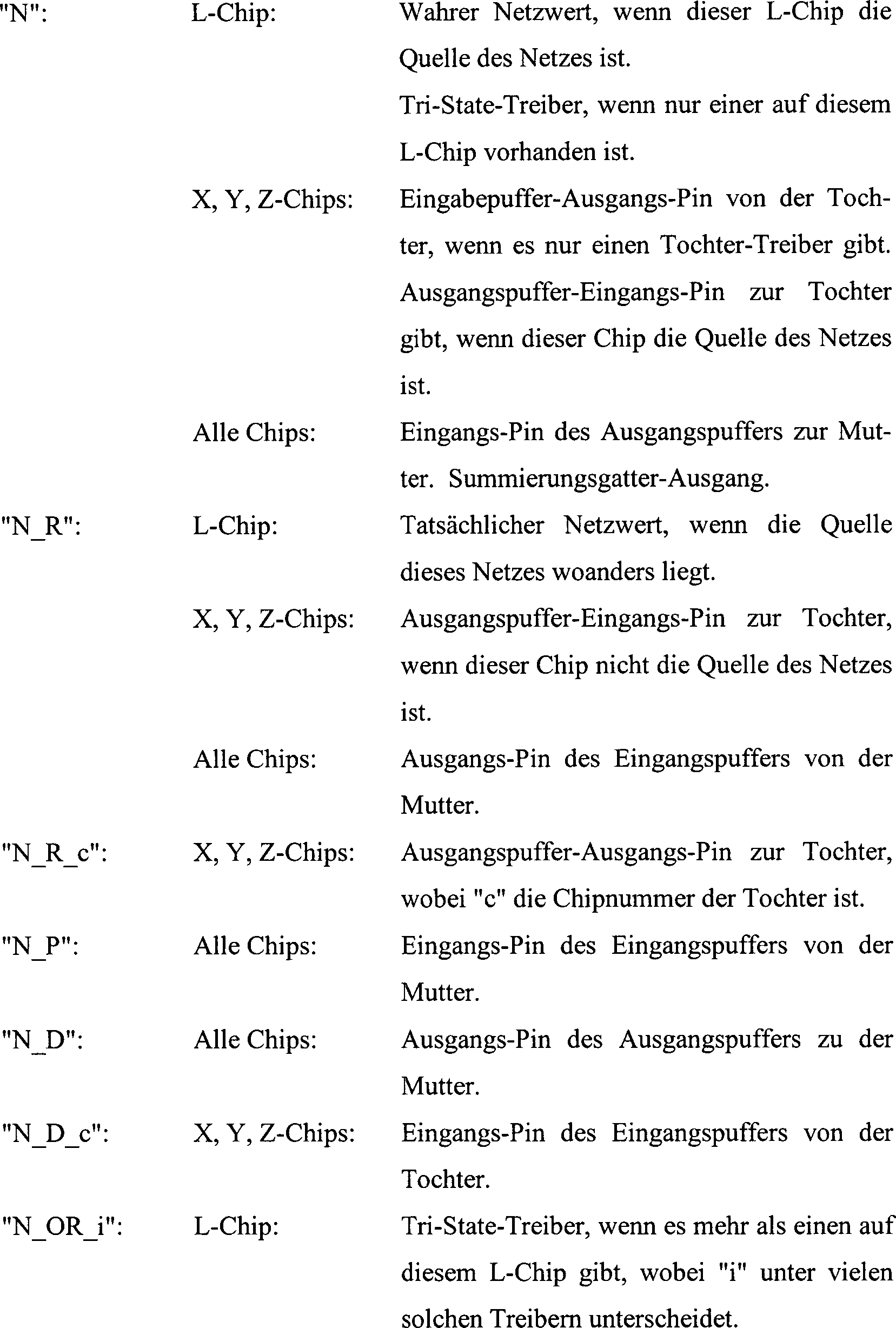

2.4.3 Stufe 1: Erzeugen der Netzlisten für die logischen Grundelemente2.4.3 Level 1: Create the netlists for the basic logic elements
Die Befehle für die Netzlisten-Dateien der Logikchips werden ein Grundelement nach dem anderen für alle logischen Grundelemente in der Entwurfsdatenstruktur ausgegeben. Die Namen der Netze, die die Pins der Grundelemente verbinden, werden vergeben, um mit den Namen, die zur Verbindung der Puffer in Stufe 3d, unten, verwendet werden, übereinzustimmen.The commands for the netlist files of the logic chips become one primitive after another all logical primitives are output in the design data structure. The names of the nets connecting the pins of the primitives are assigned to match the names used to connect the buffers in stage 3d, below.
Die Eingangs-Pins werden mit ihren wahren Netznamen verbunden, wenn die Quelle für das Netz im selben Logikchip ist, was immer für eingeschlossene Netze der Fall ist (Netze, die nicht geschnitten sind) und für den treibenden L-Chip von Schnittnetzen. Wenn dieser L-Chip nicht die Quelle ist, werden die Eingangs-Pins mit den Eingangspuffern der Mutterempfänger verbunden. Ausgangs-Pins werden mit ihren wahren Netznamen verbunden, außer wenn sie mit einem Summierungsgatter auf dem Logikchip verbunden werden. In diesem Fall werden Variationen des eindeutigen Netznamens verwendet.The Input pins are connected to their true network names when the source for the network in the same logic chip is whatever the network includes Fall is (nets that are not cut) and for the impulsive L-chip of cut nets. If this L chip is not the source, The input pins are connected to the input buffers of the mother receiver. Be output pins associated with their true net names except when using a summation gate be connected on the logic chip. In this case will be variations the unique network name.
2.4.4 Stufe 2: Erzeugen der Netzlisten für Logikchip-Summierungsgatter2.4.4 Stage 2: Create the netlists for Logic chip summing
Die Befehle für die Summierungsgatter von Tri-State-Netzen, die vollständig innerhalb eines einzelnen Logikchip enthalten sind, werden Netz nach Netz ausgegeben. Die Eingänge werden verbunden unter der Verwendung der Netznamenvariationen, die oben erwähnt sind und der Ausgang treibt den wahren Netzna men. Der geeignete Ausgangssinn (OR oder NOR) wird verwendet, je nach dem, ob das Netz "floating high" oder nicht ist.The Commands for the summation gates of tri-state networks that are completely within of a single logic chip become network after network output. The inputs are connected using the net name variations, the above mentioned and the output drives the true network. The suitable one Output sense (OR or NOR) is used depending on whether the network is "floating high" or not.
2.4.5 Stufe 3: Festlegen und Erzeugen der Netzlisten von Schnittnetz-Verbindungen2.4.5 Level 3: Set and generating the netlists of interface network connections
Für die Verbindungen von Netzen, die sich über mehr als einen Logikchip erstrecken (Schnittnetze) werden Netzlisten erzeugt. Die Schnittnetze werden nacheinander verarbeitet durch die Abfolgen der Stufen 3a, 3b und 3c für jedes Schnittnetz.For the connections of networks that are over extending more than one logic chip (meshes) become netlists generated. The cutting networks are processed one after the other the sequences of stages 3a, 3b and 3c for each cut net.
2.4.5.1 Stufe 3a: Aufbau des Verbindungsbaums2.4.5.1 Level 3a: Structure of the connection tree
Eine temporäre Baumdatenstruktur wird aufgebaut, um den Verbindungsprozeß zu führen. Er stellt die Struktur des Netzes dar, indem er die L-Chips zeigt, die Grundelemente in diesem Netz haben, die X, Y und Z-Chips, die ihre Verbindung implementieren und die Verbindungsanforderung von jedem Chip.A temporary Tree data structure is set up to guide the connection process. He represents the structure of the network by showing the L-chips, the basic elements in this network have the X, Y and Z chips, the implement their connection and the connection request from every chip.
Jeder Knoten auf jeder Ebene des Baumes entspricht einem Logik- oder Verbindungs-Chip des Systems. Er hat Äste zu den Tochterknoten unterhalb von ihm und speichert Daten über den Knoten und den Verbindungspfad zu seiner Mutter wie folgt:Everyone Node at each level of the tree corresponds to a logic or connection chip of the system. He has branches to the daughter nodes below it and stores data about that Node and the connection path to his mother as follows:

Jeder L-Chip in dem Netz wird durch einen einzigen Knoten in dem Baum dargestellt, unabhängig davon, wieviele Grundelemente er auf dem Netz hat.Everyone L-chip in the network is through a single node in the tree shown, independent of how many primitives he has on the web.
Jeder
Knoten hat die folgenden Einträge:
Wenn ein Netz nicht mehrere Boxen umfasst, hat der Root-Knoten einen Nulleintrag und nur einen Knoten auf der ersten Ebene. Wenn ein Netz nicht mehrere Karten umfasst, wird der Knoten auf der ersten Ebene einen Nulleintrag haben und nur einen Knoten auf der zweiten Ebene. Wenn ein Netz nicht mehrere L-Chips umfasst, benötigt es keine Verbindung und wird keinen Baum haben.If a network does not span multiple boxes, the root node has one Null entry and only one node on the first level. When a Net does not span multiple cards, the node becomes the first level have a zero entry and only one node on the second level. If a network does not have multiple L chips includes, needed there is no connection and will not have a tree.
Der Baum wird aufgebaut durch das Scannen des Netzes in der Entwurfsdatenstruktur gemäß der Orte der Grundelemente, die durch den Partitionierer zugewiesen worden sind. Wenn ein Netz nicht mehr als eine Box oder eine Karte umfasst, werden die Knoten für die nicht benötigten Kreuzschienenebenen mit null markiert. Daraufhin wird die Anzahl der Treiberausgänge und Empfängereingänge auf jedem L-Chip gezählt und in den L-Chip-Knoten gespeichert, um die Verbindungsanforderungen des L-Chips zu identifizieren. Die Anzahl der L-Chips, die Treiber haben und die Anzahl derer, die Empfänger haben, wird für jeden X-Chip-Knoten gezählt, um zu identifizieren, welche Verbindung von jedem X-Chip zur Verfügung gestellt werden muss. Entsprechend werden die treibenden und empfangenden X-Chips für jedes Y-Chip gezählt und die Y-Chips für den Z-Chip.Of the Tree is built by scanning the network in the design data structure according to the places the primitives that have been assigned by the partitioner are. If a network does not contain more than one box or card, become the nodes for not needed Crossbar levels marked zero. Then the number the driver outputs and receiver inputs counted every L chip and stored in the L-chip node to the connection requirements to identify the L-chip. The number of L-chips, the drivers and the number of those who have recipients will be for everyone X-chip nodes counted to to identify which connection is provided by each X chip must become. Accordingly, the driving and receiving become X chips for every Y-chip counted and the Y chips for the Z chip.
Schließlich wird der Baum analysiert, um den Punkt festzulegen, von dem der wahre Wert des Netzes, seine Quelle, an die Empfänger getrieben wird. Bei einfachen Netzen ist die Quelle einer der L-Chips. Es kann ein Kreuzschienen-Chip für ein Tri-State-Netz sein, da die Kreuzschienensummation verwendet wird. Normalerweise, wenn ein Kreuzschienen-Chip Empfänger unter seinen Tochter-Chips hat, wird in der Netzliste eingetragen, den wahren Wert von Mutter-Chip auf der höheren Ebene herunterzuleiten. Wenn jedoch ein Chip oder der Chip unter ihm in der Hierarchie die Quelle hat, dann empfängt er den wahren Wert von sich selbst oder von unten. Um dies zu erreichen, werden die Kreuzschienenknoten gescannt und wenn ein Knoten oder ein Nachkomme die Quelle ist, wird seine Empfängerzahl auf null gesetzt.Finally will the tree analyzes to determine the point from which the true Value of the network, its source to which receivers are driven. In simple Nets is the source of one of the L chips. It can be a crossbar chip for a Tri-State network because the crossbars summation is used. Normally, when a crossbar chip has receivers under its daughter chips, it gets in the netlist enlisted, the true value of mother chip on the higher Level down. However, if a chip or the chip is under he has the source in the hierarchy, then he receives the true value of yourself or from below. To achieve this, the crossbar nodes become scanned and if a node or a descendant is the source, becomes his recipient number set to zero.
2.4.5.2 Stufe 3b: Bestimmen der Fähigkeit jedes Satzes zur Verbindung2.4.5.2 Level 3b: Determine the ability every sentence to the connection
Da jeder Z-Chip mit den gleichen Y-Chips in jeder Box verbunden ist und jeder Y-Chip mit den gleichen X-Chips auf jeder Karte verbunden ist, bilden die verbundenen X-, Y- und Z-Chips einen Satz. In der bevorzugten Ausführungsform des Realizer-Systems gibt es 64 Sätze, von denen jeder aus 1 Z-Chip, 8 Y-Chips, einem in jeder Box, besteht, die Y-Z-Pfade zum Z-Chip haben und 64 X-Chips, einen auf jeder Karte, die X-Y-Pfade zu jedem Y-Chip haben. Jedes Paar von Sätzen hat die gleichen X-Chips in diesem Fall. Dies ist jedoch akzeptabel, da nur ein Set ausgewählt wird, um das Netz zu verbinden.There every Z chip is connected to the same Y chips in each box and each Y chip connected to the same X chips on each card is the connected X, Y and Z chips form a sentence. In the preferred embodiment of Realizer system, there are 64 sets, each of which consists of 1 Z chip, 8 Y chips, one in each box, have the Y-Z paths to the Z chip and 64 X chips, one on each card, have X-Y paths to each Y-chip. Each pair of sentences has the same X-chips in this case. However, this is acceptable because only one set is selected will connect to the network.
Jedes Paar von verbundenen Chips, wie zum Beispiel ein L-Chip und ein X-Chip wird durch eine Gruppe von Leitungen verbunden, die Pfade genannt werden. Die Pfade in jeder Kreuzschiene werden in einer Pfadtabelle aufgelistet. Die L-X-Pfadtabelle hat ein Element für jeden Pfad in jeder L-X-Kreuzschiene im gesamten System. Für jede Karte in jeder Box gibt es eine L-X-Kreuzschiene und für jede Kreuzschiene gibt es einen Satz von Pfaden für jeden L-Chip und jeden X-Chip. Die L-X-Pfadtabelle hat daher fünf Dimensionen: LX[Box][Karte][L-Chip][X-Chip][Pfad]. Entsprechend gibt es eine X-Y-Pfadtabelle: XY[Box][Karte][Y-Chip][Pfad] und eine Y-Z-Pfadtabelle: YZ[Box][Z-Chip][Pfad]. Jedes Element in der Tabelle wird mit "frei" oder "verwendet" durch den Verbindungsvorgang markiert. Ein Tabellenelement ist verwendet, wenn sein Pfad durch den I/O-Pin eines Eingangs- oder Ausgangspuffers verwendet wird, der an eine Netzlisten-Datei ausgegeben worden ist.each Pair of connected chips, such as an L-chip and a X-chip is connected by a group of lines, the paths to be named. The paths in each crossbar will be in a path table listed. The L-X path table has an element for every path in every L-X matrix across the system. For every card There is an L-X crossbar in each box and there is one for each crossbar Set of paths for every L chip and every X chip. The L-X path table therefore has five Dimensions: LX [Box] [Card] [L-Chip] [X-Chip] [Path]. Accordingly, there is an XY path table: XY [box] [map] [Y-chip] [path] and a Y-Z path table: YZ [box] [Z-chip] [path]. Each item in the table is used with "free" or "used" by the connection process marked. A table element is used when its path is through the I / O pin of an input or output buffer is used, which has been output to a netlist file.
Die Fähigkeit jedes Satzes, das Netz zu verbinden, wird durch das Aufsammeln der freien Pfadzahlen für jeden zu verbindenden Pfad bestimmt. Als erstes werden die Y-Z-Pfade zwischen Y-Chips in Boxen und den Z-Chips berücksichtigt. Für jede Box in dem Netz wird die Anzahl der freien Pfade in der Y-Z-Pfadtabelle für den Z-Chip und den Y-Chip dieser Box in diesem Satz gezählt und gespeichert. Als zweites werden die X-Y-Pfade zwischen X-Chips auf Karten und Y-Chips in Boxen betrachtet: Für jede Karte in dem Netz wird die Anzahl der freien Pfade in der X-Y-Pfadtabelle für den Y-Chip dieser Box und den X-Chip dieser Karte in diesem Satz gezählt und gespeichert. Als drittes werden die L-X-Pfade zwischen L-Chips und X-Chips auf den Karten berücksichtigt: Für jeden Lo gikchip in dem Netz wird die Anzahl der freien Pfade in der L-X-Pfadtabelle für diesen L-Chip und für den X-Chip dieser Karte in diesem Satz gezählt und gespeichert. Falls an irgendeiner Stelle nicht genug freie Pfade vorhanden sind, um die Verbindung durchzuführen, wird dieser Satz als Fehlschlag markiert und der Vorgang schreitet mit dem nächsten Satz fort.The ability each sentence to join the network is determined by the collection of the free path numbers for determines each path to be connected. First, the Y-Z paths considered between Y-chips in boxes and the Z-chips. For every box in the network, the number of free paths in the Y-Z path table for the Z-chip and the Y chip of that box is counted and stored in this set. As a second consider the X-Y paths between X-chips on cards and Y-chips in boxes: For every Map in the net will be the number of free paths in the XY path table for the Y-chip of this box and the X-chip of this card counted in this sentence and saved. Third, the L-X paths between L-chips and X-chips on the cards considered: For each Lo gikchip in the network will be the number of free paths in the L-X path table for this L-chip and for The X-Chip of this card is counted and stored in this set. If at some point there are not enough free paths to to perform the connection this sentence is marked as a failure and the process proceeds With the next Set forth.
Das Ergebnis ist eine Sammlung von Pfadanzahlen für jeden Pfad in der Verbindung, für jeden Satz von Kreuzschienen-Chips, die erfolgreich die Verbindung herstellen können.The Result is a collection of path numbers for each path in the connection, for each Set of crossbar chips successfully connecting can.
2.4.5.3 Stufe 3c: Auswahl des Satzes2.4.5.3 Level 3c: Selection of the sentence
Da viele Sätze in der Lage sein können, das Netz zu verbinden, wird ein Satz ausgewählt, um einen Ausgewogenheit der verwendeten Pfade zu erhalten. Dies stellt sicher, dass die volle Fähigkeit der Verbindung ausgenutzt wird.There many sentences to be able to To connect the network, a sentence is selected to balance to get the used paths. This ensures that the full ability the connection is exploited.
Eine einfache Technik zur Auswahl der Sätze würde darin bestehen, den Satz auszuwählen mit der größten Gesamtpfadanzahl. Dies ignoriert jedoch lokale Bedingungen. Es ist besser, den Satz auszuwählen, der die größte minimale Pfadzahl unter den Pfadzahlen auf allen Ebenen hat. Beispielsweise seien zwei Sätze mit diesen Pfadzahlen angenommen:A Simple technique for selecting the sentences would be to use the sentence select with the largest total number of paths. However, this ignores local conditions. It is better the sentence to select the the biggest minimum Has path number among the path numbers at all levels. For example be two sentences with assumed these path numbers:

Satz A hat die größte Gesamtanzahl (23 gegenüber 21), aber die Auswahl dieses Satzes würde bedeuten, dass der letzte zur Verfügung stehende L-X-Pfad von einem L-Chip-X-Chip-Paar verwendet würde. Satz B hat das größte Minimum (3 gegenüber 1) und würde kein L-Chip-X-Chip-Paar ausschließen. Im Fall von gleichen Werten lasse ein Minimum von jedem Satz außer Betracht und wähle den Satz aus mit dem größten verbleibenden Minimum, und so weiter, bis ein Satz ausgewählt ist. Wenn alle Sätze tatsächlich gleich sind (wie es der Fall für das erste Netz ist), wähle irgendeines aus. Dies ist das verwendete Verfahren. Eine Spezialbetrachtung wird angewendet, wenn ein Satz für ein Tri-State-Netz betrachtet wird. Da einige Paare der Chips zwei Pfade haben müssen, die für dasselbe Netz verwendet werden, einen für einen Eingang, der in der Hierarchie nach oben bis zum Summierungsgatter verläuft und der andere, der den tatsächlichen Wert wieder nach unten zurückbringt, muss der ausgewählte Satz zumindest zwei freie Pfade für diese Fälle haben. Solch ein Fall wird detektiert, wenn der Knoten am Baum des Pfades (d. h. der X-Chip-Knoten für einen L-X-Pfad etc.) von null verschiedene D- und R-Zählwerte hat und ein Mutter, die nicht null ist.sentence A has the largest total number (23 opposite 21), but the choice of this sentence would mean that the last one to disposal standing L-X path would be used by a L-chip X-chip pair. sentence B has the biggest minimum (3 opposite 1) and would do not exclude an L-chip X-chip pair. In the case of equal values ignore a minimum of each sentence and choose the one Set off with the largest remaining Minimum, and so on, until a sentence is selected. If all sentences are actually the same are (as is the case for the first network is), choose any one. This is the method used. A special consideration is applied when a sentence for a tri-state network is considered. As some pairs of chips two Have to have paths the for the same network, one for an input, in the hierarchy goes up to the summation gate and the other, the actual Value back down again, must be the selected one Set to have at least two free paths for these cases. Such a case will detected when the node on the tree of the path (i.e., the X-chip node for one L-X path etc.) from zero different D and R counts and a nut, which is not null.
2.4.5.4 Stufe 3d: Erzeugen der Netzlisten für die Verbindung2.4.5.4 Level 3d: Create the netlists for the connection
Bei einer gegebenen Auswahl eines Satzes und einer gegebenen Baumstruktur wird die Netzliste für die Verbindung erzeugt, indem Befehle für die Puffer und die Summierungsgatter an die Logik- und Verbindungs-Chip-Netzlisten-Dateien ausgegeben werden. Dies wird Ebene nach Ebene durchgeführt, zuerst die Logikchips, dann X, Y und Z-Chips. Die Verbindungen von jedem Chip und die Richtungen werden bestimmt, indem die Daten in dem Baum verwendet werden. Jede Verbindung wird in eine Netzlisten-Datei eingetragen, indem die Befehle für die Puffer der Verbindungen und für die Netze an eine Netzlisten-Datei ausgegeben werden. Die Verbindungen eines Chips an Tochterchips (falls vorhanden) werden zuerst in die Netzlisten-Dateien eingetragen. Jeder Tochterchip wird wiederum berücksichtigt. Wenn der Baum zeigt, dass er diesen Chip treibt, wird ein Eingabepuffer in die Netzlisten-Datei eingetragen unter der Verwendung der Nummer des Pins, der mit dem Treiber des Tochterchips verbunden ist. Wenn dieser Chip mehr als einen Treiber hat, werden unterschiedliche Netznamen für jeden verwendet, so dass sie durch das später in der Netzlisten-Datei aufgeführte Summierungsgatter aufgesammelt werden können. Wenn der Baum zeigt, dass die Tochter diesen Chip empfängt, wird ein Ausgangspuffer in der Netzlisten-Datei hinzugefügt, unter der Verwendung der Nummer des Pins, der mit dem Empfänger des Tochterchips verbunden ist. Wenn dieser Chip selbst ein Empfänger von seinem Mutterchip ist, wird ein anderer Netzname verwendet, damit er mit dem Mutterempfänger in Verbindung steht.Given a selection of a set and a given tree, the netlist for the connection is generated by issuing commands for the buffers and the summation gates to the Logic and Link Chip netlist files. This is done level by level, first the logic chips, then X, Y and Z chips. The connections of each chip and the directions are determined by using the data in the tree. Each connection is entered into a netlist file by issuing the commands for the buffers of the connections and for the networks to a netlist file. The connections of a chip to daughter chips (if any) are first entered into the netlist files. Each daughter chip is considered again. If the tree shows that it is driving this chip, an input buffer is entered into the netlist file using the pin number associated with the daughter chip's driver. If this chip has more than one driver, different net names are used for each so that they can be picked up by the summation gate listed later in the netlist file. If the tree shows that the daughter is receiving this chip, an output buffer is added in the netlist file using the number of the Pins connected to the receiver of the daughter chip. If this chip itself is a recipient of its mother chip, another network name is used to connect to the mother receiver.
Wenn dieser Chip mehr als einen Treiber unter seinen Töchtern hat, wird das Summierungsgatter der Netzlisten-Datei hinzugefügt und dadurch mit den Treibernetzen, die oben definiert worden sind, verbunden. Schließlich werden die Verbindungen zu dem Mutter-Chip (falls vorhanden) in der Netzlisten-Datei hinzugefügt. Wenn dieser Chip oder irgendein Nachfolger einen Treiber hat, wird ein Verbindungspfad für den Treiber vom Pfadtabelleneintrag für dieses Paar von Chips entnommen und der Satz, der ausgewählt worden ist, und ein Ausgangspuffer wird in die Netzlisten-Datei eingetragen, um den mutter-Chip über den gerade entnommenen Pfad zu treiben. Wenn dieser Chip ein Empfänger vom Mutter-Chip ist, wird ein Pfad aus der Pfadtabelle entnommen und ein Eingangspuffer, der diesen Pfad verwendet, wird in die Netzlisten-Datei eingetragen.If this chip has more than one driver among its daughters, the summation gate is added to the netlist file and thereby with the driver networks that have been defined above. Finally the connections to the mother chip (if any) in the netlist file added. If this chip or any successor has a driver, it will a connection path for taken the driver from the path table entry for this pair of chips and the sentence that selected has been, and an output buffer is in the netlist file entered to the mother chip over to drive the just taken path. If this chip is a receiver from Mother chip is, a path is taken from the path table and an input buffer, which uses this path is entered in the netlist file.
2.4.6 Detaillierte Definition des Vorgangs zur Verbindung und zur Erstellung der Netzlisten-Dateien. Zunächst einige allgemeine Definitionen:2.4.6 Detailed definition the process of connecting and creating netlist files. First, some general definitions:
Es
gibt vier Klassen von Netzen:
Die "Quelle" eines Netzes ist
der Chip, der seinen aktuellen logischen Wert treibt:
Für einfache
Netze ist dies der L-Chip, der den Treiber hat.
Für ein Tri-State-Netz,
ist es der Chip, der das oberste Summierungsgatter hat.
Um
die Quelle zu bestimmen:
Scanne das Netz, um zu sehen, wo sich
die Ausgangs-Pins befinden.
Wenn sie sich alle auf dem gleichen
L-Chip befinden, ist dies die Quelle.
Andernfalls, wenn sie
alle auf der gleichen Karte sind, ist es der X-Chip auf dieser Karte.
Andernfalls,
wenn sie alle in der gleichen Box sind, ist es der Y-Chip in dieser
Box.
Andernfalls ist es der Z-Chip.The "source" of a network is the chip that drives its current logical value:
For simple networks, this is the L-chip that has the driver.
For a tri-state network, it is the chip that has the top summation gate.
To determine the source:
Scan the mesh to see where the output pins are.
If they are all on the same L-chip, this is the source.
Otherwise, if they're all on the same card, it's the X chip on that card.
Otherwise, if they're all in the same box, it's the Y chip in that box.
Otherwise, it is the Z chip.
Eine Ausgangs-Pin-Indexnummer gibt an, welcher Ausgangs-Pin es in der zirkularen Liste der Pins seines Netzes ist, beginnend von dem Pin, auf den der Netzeintrag zeigt und durch Abzählen von Null beginnend.A Output pin index number indicates which output pin is in the circular list of the pins of its network, starting from the pin, pointed to by the net entry and starting by counting from zero.
Stufe 1: Ausgabe aller Grundelemente in der EntwurfsdatenstrukturStage 1: Output of all Basic elements in the design data structure
Für jeden
L-Chip in der Entwurfsdatenstruktur:
Öffne die Netzlisten-Datei dieses
L-Chips, wenn sie nicht bereits offen ist.
Für jedes
Grundelement auf diesem L-Chip:
Gib die Kopfbefehlszeile für das Grundelement
an die Datei aus:
Für
jeden Pin dieses Grundelements:
Nimm den Namen des verbundenen
Netzes (unter Verwendung der Identifizierung des Objekts des Netzes, um
ihn aus der Eingabeentwurfsdatei zu erhalten) und Bezeichne ihn "N".
Falls es sich um ein Input-Pin
handelt:
Wenn dieser L-Chip die Quelle des Netzes hat, gib
einen Befehl aus für
einen Eingangs-Pin, der mit dem Netz "N" verbunden
ist.
Andernfalls gib einen Eingangs-Pin-Befehl an das Netz "N_R" aus.
Andernfalls
(falls es sich um einen Ausgangs-Pin handelt):
Nimm die Indexnummer
dieses Ausgangs-Pins und bezeichne sie "p".
Wenn
es ein einfaches Netz ist, gib Pin auf Netz "N" aus.
Wenn
es ein Tri-State eingeschlossenes Netz ist, gib Pin auf Netz "N_OR_p"aus.
Wenn es
ein Tri-State-Schnittnetz ist:
Falls dies der einzige Ausgang
auf diesem Netz auf diesem L-Chip ist, gib Pin auf Netz "N" aus.
Andernfalls gib Pin auf Netz "N_OR_p" aus.
Nächster Pin
Nächstes Grundelement
Nächster L-Chip.For each L-chip in the design data structure:
Open the netlist file of this L-chip if it is not already open.
For every primitive on this L-Chip:
Issue the header command line for the primitive to the file:
For each pin of this primitive:
Take the name of the connected network (using the identification of the object of the network to get it from the input design file) and designate it "N".
If it is an input pin:
If this L-chip has the source of the network, issue a command for an input pin connected to the network "N".
Otherwise, issue an input pin command to the network "N_R".
Otherwise (if it is an output pin):
Take the index number of this output pin and label it "p".
If it is a simple network, issue pin on network "N".
If it is a tri-state trapped network, issue pin on network "N_OR_p".
If it is a tri-state mesh:
If this is the only output on this network on this L chip, issue pin on network "N".
Otherwise, issue pin on network "N_OR_p".
Next pin
Next primitive
Next L chip.
Stufe 2: Gib alle Summierungsgatter für eingeschlossene Netze ausStage 2: Give all summation gates for trapped Networks off
Für jedes
eingeschlossene Tri-State-Netz:
Nimm den Namen dieses Netzes
und bezeichne es mit "N".
Öffne die
Netzlisten-Datei dieses L-Chip, wenn sie nicht bereits offen ist.
Zähle, wieviele
Ausgänge
sich auf dem Netz befinden und bezeichne dies mit "i".
Gib Befehle aus für ein Gatter
mit "i"-Eingängen:
NOR,
falls dieses Netz auf "floating-high" ist, andernfalls
OR,
wobei die Eingänge
mit den Netzen "N_OR_j" verbunden sind,
(für alle
j von 0 bis i – 1)
und
wobei der Ausgang mit "N" verbunden ist.
Nächstes Netz.For each included tri-state network:
Take the name of this net and name it "N".
Open the netlist file of this L-chip if it is not already open.
Count how many outputs are on the network and label this as "i".
Issue commands for a gate with "i" inputs:
NOR, if this net is floating-high, otherwise OR,
the inputs being connected to the networks "N_OR_j", (for all j from 0 to i-1)
and wherein the output is connected to "N".
Next network.
Stufe 3: Gib die Puffer aus, die die Schnittnetze verbinden und gib die Summierungsgatter aller Schnittnetze ausStage 3: Give the buffers out that connect the cut nets and give the summation gates of all cutting nets
Markiere
alle Elemente von allen Verbindungspfadtabellen als "frei".
Für jedes
Schnittnetz (einfach oder Tri-State).
Wähle Schnittnetze in der Reihenfolge
der Hierarchie aus, zuerst Multi-Boxnetze,
etc. und innerhalb dieser Reihenfolge die größten zuerst:Mark all elements of all connection path tables as "free".
For every cutting net (simple or tri-state).
Select cutting nets in the order of the hierarchy, first multi-box nets, etc. and within this order the largest ones first:
Stufe 3A: Baue den Baum aufStage 3A: Build the tree on
Für jedes
Grundelement des Netzes:
Wenn es keinen Baumknoten für die Box
dieses Grundelementes gibt, füge
einen hinzu.
Wenn es keinen Baumknoten für die Karte dieses Grundelementes
in dieser Box gibt, füge
einen hinzu.
Wenn es keinen Baumknoten für den L-Chip dieses Grundelementes
auf dieser Karte in dieser Box gibt, füge einen hinzu.
Wenn die
Netzverbindung dieses Grundelementes ein Ausgangs-Pin ist (d. h.
treibend), erhöhe
den D-Zählwert
an diesem Knoten des L-Chips.
Andernfalls, wenn dieser L-Chip
nicht die Quelle für
dieses Netz ist, erhöhe
den R-Zählwert
auf dem Knoten dieses L-Chips.
Nächstes Grundelement.
Nachdem
alle Grundelemente dieses Netzes in dem Baum dargestellt sind, markiere
den Y-Chipknoten NULL, wenn es nur einen X-Chipknoten gibt (d. h.
das Netz bleibt auf der Karte).
Wenn es nur einen Y-Chipknoten
gibt, Markiere den Z-Chipknoten mit NULL. (Das Netz bleibt innerhalb
der Box).
Für
jede Kreuzschienenebene die nicht NULL ist, zuerst X-Chip, dann
Y-Chip, dann Z-Chip:
Für
jeden Knoten auf dieser Ebene:
D = die Anzahl der Tochter-Knoten,
die D-Zählwerte
ungleich Null haben,
R = die Anzahl der Tochter-Knoten, die
R-Zählwerte
haben, die ungleich Null sind.
Wenn dieser Knoten oder ein
Nachkomme die Quelle dieses Netzes ist, setze R von diesem Knoten
auf 0.
Wenn dieser Knoten die Quelle ist und das Netz ein Tri-State-Netz
ist, setze sein "top
sum" Flag auf wahr.
Nächster Knoten.
Nächste Ebene.For each basic element of the network:
If there is no tree node for the box of this primitive, add one.
If there is no tree node for the map of this primitive in this box, add one.
If there is no tree node for the L-chip of this primitive on this card in this box, add one.
If the network connection of this primitive is an output pin (ie, driving), increase the D count on that node of the L chip.
Otherwise, if this L-chip is not the source for this network, increase the R-count on the node of that L-chip.
Next primitive.
After all the primitives of this network are shown in the tree, mark the Y-chip node NULL if there is only one X-chip node (ie the network stays on the card).
If there is only one Y-chip node, mark the Z-chip node with ZERO. (The net stays inside the box).
For each crossbar level that is not NULL, first X-Chip, then Y-Chip, then Z-Chip:
For each node at this level:
D = the number of daughter nodes that have nonzero D counts,
R = the number of daughter nodes that have R counts that are nonzero.
If this node or descendant is the source of this network, set R from this node to 0.
If this node is the source and the network is a tri-state network, set its "top sum" flag to true.
Next node.
Next level.
Stufe 3B: Bestimme die Fähigkeit zur Verbindung von jedem SatzLevel 3B: Determine the ability to connect each sentence
Für jeden
Satz: Bestimme seine Fähigkeit
zur Verbindung durch das Aufsammeln der Pfadzähler für jeden Pfad, der verbunden
werden soll:
Weise Speicherplatz für die Pfadzähler dieses Satzes zu:
Y-Z-Pfadzähler: einen
für jede
Box,
X-Y-Pfadzähler:
einen für
jede Karte,
L-X-Pfadzähler:
einen für
jeden L-Chip.
Falls es nur eine Box in diesem Netz gibt (eine
Z-Ebenenverbindung wird nicht benötigt):
Lasse einen Null
Y-Z-Pfadzähler
für diese
Box.
Andernfalls:
Für
jede Box:
Zähle
die Anzahl der freien Pfade in dem Pfadfeld YZ [diese Box] [dieser
Satz] [Pfade].
Wenn der Baumknoten dieser Box eine Mutter hat,
die nicht NULL sind, und D > 0
ist und R > 0 ist:
Dieser
Pfad der Box ist "doppelt": er hat sowohl einen
Treiber als auch einen Empfänger.
Wenn
weniger als zwei freie Pfade vorhanden sind, kann dieser Satz dieses
Netz nicht verbinden.
Andernfalls, wenn keine Pfade vorhanden
sind, kann dieser Satz dieses Netz nicht verbinden.
Wenn dieser
Satz nicht verbinden kann, markiere ihn als unverwendbar und fahre
mit dem nächsten
Satz fort.
Andernfalls Speichere das Gesamte als die Y-Z-Pfadzahl
für diese
Box.
Wenn es nur eine Karte in diesem Netz gibt (eine Y-Z-Verbindung wird dann
nicht benötigt):
Belasse
den X-Y Pfadzähler
auf Null für
diese Karte:
Andernfalls:
Für jede Karte:
Zähle die
Anzahl der freien Pfade in dem Pfadfeld XY [diese Box] [diese Karte]
[dieser Satz] [Pfade]
Wenn dieser Pfad "doppelt" ist und < zwei Paare vorhanden sind, oder wenn
keine Pfade vorhanden sind, kann dieser Satz dieses Netz nicht verbinden:
Markiere
diesen Satz als nicht verwendbar, und fahre mit dem nächsten Satz
fort.
Andernfalls speichere die Gesamtheit als den X-Y-Pfadzähler für diese
Karte.
Für
jeden L-Chip:
Zähle
die Anzahl der freien Pfade in dem Pfadfeld LX [diese Box] [diese
Karte] [dieser L-Chip] [dieser Satz] [Pfade].
Wenn dieser Pfad "doppelt" ist, und weniger
als zwei Pfade vorhanden sind, oder wenn keine Pfade vorhanden sind,
kann dieser Satz nicht dieses Netz verbinden: Markiere diesen Satz
als nicht verwendbar und fahre mit dem nächsten Satz fort.
Andernfalls
Speichere die Gesamtheit als die L-X Pfadzahl für diesen L-Chip.
Nächster L-Chip
auf dieser Karte:
Nächste
Karte in dieser Box.
Nächste
Box.
Nächster
Satz.For each sentence: Determine its ability to connect by collecting the path counters for each path to be connected:
To allocate space for the path counters of this set:
YZ path counter: one for each box,
XY path counter: one for each card,
LX path counter: one for each L chip.
If there is only one box in this network (a Z-level connection is not needed):
Leave a zero YZ path counter for this box.
Otherwise:
For each box:
Count the number of free paths in the path field YZ [this box] [this set] [paths].
If the tree node of this box has a parent that is not NULL and D> 0 and R> 0:
This path of the box is "double": it has both a driver and a receiver.
If less than two free paths exist, this set can not join this network.
Otherwise, if there are no paths, this set can not join this network.
If this sentence can not connect, mark it as unusable and proceed to the next sentence.
Otherwise, save the total as the YZ path number for this box.
If there is only one card in this network (a YZ connection is not needed):
Leave the XY path counter at zero for this card:
Otherwise:
For each card:
Count the number of free paths in the path field XY [this box] [this card] [this set] [paths]
If this path is "double" and there are <two pairs, or if there are no paths, that set can not join this network:
Mark this sentence unusable and proceed to the next sentence.
Otherwise, save the whole as the XY path counter for this card.
For every L chip:
Count the number of free paths in the path field LX [this box] [this card] [this L-chip] [this set] [paths].
If this path is "double" and there are less than two paths, or if there are no paths, that set can not connect to that network: mark this set as unusable and proceed to the next sentence.
Otherwise, save the ensemble as the LX path number for this L-chip.
Next L chip on this card:
Next card in this box.
Next box.
Next sentence.
Stufe 3C: Auswahl des SatzesStage 3C: Selection of the record
Für jeden
Satz, der das Netz verbinden kann:
Finde den minimalen Pfadzähler unter
allen Pfadzählern
für diesen
Satz. Nächster
Satz.
Finde den größten von
allen diesen minimalen Pfadzählern.
Eliminiere
von der Betrachtung alle Sätze
mit Pfadzählern,
die kleiner sind als das größte Minimum.
Wenn
kein Satz übrig
ist, dann kann dieses Netz nicht verbunden werden.
Wenn ein
Satz übrig
ist, dann ist dieser Satz für
dieses Netz ausgewählt
worden.
Wenn mehr als ein Satz übrig ist,
finde das nächste größte Minimum
unter allen minimalen Pfadzählern.
eliminiere
aus der Betrachtung alle Sätze
mit Pfadzählern,
die kleiner sind.
Wiederhole dies, bis entweder ein Satz übrig ist
oder alle übrigen
Sätze die
gleichen Pfadzähler
haben.
Wähle
irgendeines von den übrigen
Sätzen
für dieses
Netz aus.
Gib den Speicherbereich für die Pfadzähler für alle diese Sätze frei.For every sentence that can connect the network:
Find the minimum path counter among all path counters for this set. Next sentence.
Find the largest of all these minimal path counters.
Eliminate from consideration all sentences with path counters smaller than the largest minimum.
If no sentence is left, then this net can not be connected.
If a sentence is left, then that sentence has been selected for that network.
If more than one sentence is left,
find the next largest minimum among all minimum path counters.
eliminate from consideration all sentences with path counters which are smaller.
Repeat this until either one sentence is left or all other sentences have the same path counter.
Select any of the remaining sentences for this network.
Free the memory area for the path counters for all these records.
Stufe 3D: Erzeuge die Netzlisten-Dateien für die VerbindungStage 3D: Create the Netlist files for the connection
Definitionen der weiter unten verwendeten ProzedurenDefinitions of the next procedures used below
Um einen Treiber-(oder Empfänger-)Pfad zu bekommen und zu reservieren:
- 1) Wähle einen Pfad von einem freien Element in der Pfadtabelle für diese Ebene aus, die Chipnummer dieses Knotens, und die Chipnummer des Mutter-Knotens.
- 2) Markiere das Element der Pfadtabelle als verwendet.
- 3) Speichere, welcher Pfad als Pfadnummer in dem Treiber (oder Empfänger)-Pfadnummerneintrag für diesen Knoten verwendet worden ist.
- 1) Select a path from a free element in the path table for that layer, the chip number of that node, and the mother node's chip number.
- 2) Mark the element of the path table as used.
- 3) Store which path has been used as the path number in the driver (or receiver) path number entry for this node.
Um eine I/O Pin-Nummer abzuleiten:
- 1) Bestimme die Identitäten der Chips von diesem Knoten und der Chips des Tochterknotens (oder der Chips des Mutter-Knotens, je nach Fall) aus den Chipnummern der beiden Knoten und der Satznummer. Dies identifiziert den speziellen betroffenen Pfad (wie z. B. L4–X5, oder Karte 3–Y7).
- 2) Erinnere Dich daran, dass die Pfadnummer einen der verschiedenen Pfade bezeichnet, die ein Paar von Chips miteinander verbinden. Bei gegebenem Chip, Pfad und Pfadnummer, lies die Pin-Nummer, die diesen Pfad verbindet, aus der Tabelle, die die I/O Pin-Nummerninformation enthält.
- 1) Determine the identities of the chips from this node and the daughter node chips (or mother node chips, as appropriate) from the chip numbers of the two nodes and the block number. This identifies the particular affected path (such as L4-X5, or Map 3-Y7).
- 2) Remember that the path number designates one of the different paths connecting a pair of chips. For a given chip, path and path number, read the pin number that connects this path from the table that contains the I / O pin number information.
Um einen Puffer (Eingang oder Ausgang) unter der Verwendung eines Pfades auszugeben:
- 1) Nimm die Pfadnummer dieses Knotens oder wenn ein Tochter-Pfad spezifiziert ist, nimm ihn vom Tochter-Knoten. Nimm die Treiber- oder Empfängerpfadnummer wie angewiesen.
- 2) Leite die I/O Pin-Nummer dieses Puffers ab unter der Verwendung der Pfadnummer.
- 3) Gib Grundelement-Befehle an die Netzlisten-Datei für den Chip dieses Knotens heraus, entsprechend, ob es ein Eingangs- oder ein Ausgangspuffer ist, unter Verwendung der Eingangs- und Ausgangsnetznamen, wie angewiesen, und unter der Verwendung der abgeleiteten Pin-Nummern für seinen I/O Pin.
- 1) Take the path number of this node or if a daughter path is specified, take it from the daughter node. Take the driver or receiver path number as instructed.
- 2) Derive the I / O pin number of this buffer using the path number.
- 3) Issue primitive commands to the netlist file for that node's chip, whether it is an input or output buffer, using the input and output network names as instructed, and using the derived pin numbers for his I / O pin.
Prozedur
zum Erzeugen der Netzlisten-Datei der Verbindung:
Nimm den
Namen dieses Netzes, bezeichne es mit "N".
Für jede Ebene,
die nicht NULL ist, zuerst L-Chip, dann X-Chip, dann Y-Chip und
Z-Chip:
Für
jeden Knoten auf dieser Ebene über
den gesamten Baum:
Öffne
die Netzlisten-Datei für
den Chip dieses Knotens, wenn sie nicht bereits geöffnet ist.
Wenn
die Ebene X, Y oder Z ist: für
jeden Tochterknoten unter diesem Knoten:
Setze einen Zähler "i" auf Null.
Wenn das D der Tochter > 0 ist: (die Tochter
ist Treiber)
Wenn das D dieses Knotens = 1 ist:
Gib einen
Eingangspuffer aus, von "N_D_c" bis "N", (wobei "c" die
Nummer des Tochterknotens ist) unter der Verwendung des Pfades des
Treibers der Tochter.
Andernfalls, wenn das D dieses Knotens > 1 ist:
Gib einen
Eingangspuffer von "N_D_c" bis "N_OR_i" aus unter Verwendung
des Treiberpfades der Tochter, und erhöhe "i".
Wenn
das R des Kindes > 0
ist: (die Tochter ist Empfänger)
Wenn
das D dieses Knotens > 0
ist und das R dieses Knotens = 0 ist:
Gib einen Ausgangspuffer
von "N" bis "N_R_c" aus unter Verwendung
des Empfängerpfades
des Kindes.
Andernfalls:
Gib einen Ausgangpuffer von "N_R" bis "N_R_c" unter Verwendung
des Empfängerpfades
der Tochter aus.
Nächster
Kinderknoten.
wenn das D dieses Knotens > 1 ist: (der Knoten hat ein Summierungsgatter)
Gib
ein Gatter mit "i" Eingangen aus:
NOR,
wenn dieses Netz auf "floating-high" ist, und wenn das "top sum"-Flag dieses Knotens
wahr ist. Andernfalls ein OR,
wobei die Eingänge auf "N_OR_j" verbunden sind (für alle j
von 0 bis i – 1),
und
die Ausgänge
mit "N" verbunden sind.
Wenn
das D dieses Knotens > 0
ist und eine Mutter hat, die nicht NULL ist: (der Knoten ist Treiber)
Nimm
und Reserviere einen Treiberpfad.
Gib einen Ausgangsfpuffer
von "N" bis "N_D" aus, unter Verwendung
des Treiberpfades.
Wenn das R dieses Knotens > 0 ist: (der Knoten
ist Empfänger)
Nimm
und reserviere einen Empfängerpfad.
Gib
einen Eingangspuffer für "N_P" bis "N_R" aus, unter Verwendung
des Empfängerpfades.
Nächster Knoten
auf dieser Ebene
Nächste
Ebene.
Nächstes
Schnittnetz.
Schließe
alle offenen Netzlisten-Dateien.Procedure for creating the netlist file of the connection:
Take the name of this net, label it "N".
For each non-zero level, first L-chip, then X-chip, then Y-chip and Z-chip:
For every node on this level over the entire tree:
Open the netlist file for that node's chip if it's not already open.
If the level is X, Y or Z: for each child node below this node:
Set a counter "i" to zero.
If the daughter's D is> 0: (the daughter is the driver)
If the D of this node = 1:
Output an input buffer from "N_D_c" to "N" (where "c" is the child node number) using the path of the daughter's driver.
Otherwise, if the D of this node is> 1:
Output an input buffer from "N_D_c" to "N_OR_i" using the daughter's driver path and increment "i".
If the child's R is> 0: (the daughter is the recipient)
If the D of this node is> 0 and the R of this node = 0:
Output an output buffer from "N" to "N_R_c" using the child's receiver path.
Otherwise:
Output an output buffer from "N_R" to "N_R_c" using the daughter's receiver path.
Next child node.
if the D of this node is> 1: (the node has a summation gate)
Give a gate with "i" inputs:
NOR, if this net is floating-high and if the top sum flag of this node is true. Otherwise an OR,
the inputs being connected to "N_OR_j" (for all j from 0 to i-1),
and the outputs are connected to "N".
If the D of this node is> 0 and has a non-zero mother: (the node is driver)
Take and reserve a driver path.
Output an output buffer from "N" to "N_D" using the driver path.
If the R of this node is> 0: (the node is the receiver)
Take and reserve a receiver path.
Output an input buffer for "N_P" to "N_R" using the receiver path.
Next node on this level
Next level.
Next cut net.
Close all open netlist files.
2.4.7 Zwei Beispielnetze2.4.7 Two example networks
Der
Verbindungsbaum, der durch Stufe 3a für dieses Netz gebaut wird,
ist in
Die
tatsächlichen
Gatter und Puffer, die an die Netzlisten-Dateien für jeden
Logik- und Kreuzschienenchip ausgegeben werden und wie sie miteinander
verbunden sind, ist in
Der
Verbindungsbaum, der durch Stufe 3a für dieses Netz gebaut wird,
ist in
Die
tatsächlichen
Gatter und Puffer die an die Netzlisten-Datei für jeden Logik- und Verbindungs-Chip ausgegeben
werden ist ebenso wie ihre Verbindung in
3. Realizer-System-Anwendungen3. Realizer system applications
3.1 Realizer-Logik-Simulations-System3.1 Realizer Logic Simulation System
Ein Logiksimulator ist ein System das in Hardware oder Software implementiert ist, und das ein Eingabeentwurf, einen Satz von Stimulation für den Entwurf, und eine Anweisung zur Simulation für eine Zeitperiode empfängt, und das einen Satz von Antworten erzeugt, die Antworten vorhersagen die eine tatsächliche Implementierung des Eingabeentwurfs bei derselben Stimulation erzeugen würde. Die Stimulation und die Antworten bestehen aus logischen Zustandsänderungen von spezifizierten Entwurfnetzen zu spezifizierten Zeiten. Eine wichtige Eigenschaft ist, dass der Simulatoranwender nur die Beschreibung eines Entwurfs in der Form einer Eingabe-Entwurfsdatei liefert, so dass der Entwurf verändert werden kann und innerhalb von kurzer Zeit resimuliert werden kann.One Logic simulator is a system implemented in hardware or software and that's an input design, a set of stimulation for the design, and receive an instruction for simulation for a period of time, and that generates a set of answers that predict answers the one actual implementation of the input design at the same stimulation. The Stimulation and responses consist of logical state changes specified design nets at specified times. A important feature is that the simulator user only the description a design in the form of an input design file, so that the design changes can be resuscitated within a short time.
Es ist die gängige Praxis eines Softwarelogik-Entwurfssimulator, ein Computer-Softwareprogramm zu verwenden, das einen sequentiellen Algorithmus ausführt, der den Betrieb des Entwurfs vorhersagt ("An Introduction to Digital Simulation", Mentor Graphics Corp., Beaverton Oregon, 1989). Entweder werden Ereignisgetriebene oder compilierte Code-Algorithmen, die wohlbekannt sind, verwendet. Die gegenwärtige Praxis eines Hardwarelogik-Entwurfssimulators ist es, Hardware zu bauen, die dieselben ereignis-getriebenen oder aus compiliertem Code bestehenden sequentiellen Algorithmen ausführt, die in Software-Simulatoren verwendet werden. Die Hartware bekommt ihren Performance-Vorteil lediglich durch das Ausnützen von Parallelismen in dem Algorithmus und/oder durch das direkte Implementieren von speziellen algorithmischen Operationen, die für eine Ausführungs-Software auf einem Mehrzweck-Computer nicht möglich sind. Ge genwärtige Hardwarelogik-Simulatoren arbeiten durch das Ausführen eines sequentiellen Algorithmus, der die Antworten des Eingabeentwurfs vorhersagt.It is the common one Practice of a software logic design simulator, a computer software program to use a sequential algorithm that performs predicts the operation of the design ("Introduction to Digital Simulation", Mentor Graphics Corp., Beaverton Oregon, 1989). Either become event-driven or compiled code algorithms that are well known. The current one The practice of a hardware logic design simulator is to add hardware build the same event-driven or compiled ones Code executes existing sequential algorithms used in software simulators be used. The hardware gets its performance advantage only by exploiting of parallelisms in the algorithm and / or by the direct Implement special algorithmic operations necessary for execution software on a multi-purpose computer are not possible. Ge currently hardware logic simulators work by running a sequential algorithm that analyzes the responses of the input design predicts.
Ein neues Mittel zum Bau eines Logik-Simulators basiert auf dem Realizer-System. Das Realizer-Logik-Simulator-System empfängt einen Eingabeentwurf, den es in eine Konfiguration der Logik- und Verbindungschips der Realizer Hardware konvertiert, unter Verwendung des Realizer-Entwurfs-Konversions-Systems. Es nimmt einen Stimulationssatz für den Entwurf und eine Anweisung zum Simulieren über einen Zeitraum hinweg auf, wendet diese Stimulation auf den realisierten Entwurf über Vektor-Speicher an, und sammelt einen Antwortsatz vom realisierten Entwurf über Verctor-Speicher auf. Die Antworten entsprechen denen, die eine tatsächliche Implementierung des Eingabeentwurfs bei derselben Stimulation produzieren würde, da die Antwort auf die Stimulation einer tatsächlichen Hardware-Realisierung des Entwurfs beobachtet wird.A new means of constructing a logic simulator is based on the Realizer system. The Realizer Logic Simulator system receives an input design that it converts to a Realizer hardware logic and interconnect configuration using the Realizer Design Conversion Sys tems. It picks up a design stimulus and a simulation instruction over a period of time, applies that stimulus to the realized design via vector memory, and collects a response sentence from the realized design via Verctor memory. The responses are the same as those that would produce an actual implementation of the input design on the same stimulus since the response to the stimulation of an actual hardware implementation of the design is observed.
Dies unterscheidet sich fundamental von allen gegenwärtigen Logik-Simulations-Systemen dadurch, dass diese einen sequentiellen Algorithmus ausführen, der die Entwurfsantworten auf eine Stimulation vorhersagt, während der Realizer-Logik-Simulator eine tatsächliche Realisierung des Entwurfs betreibt, um die Antworten des Entwurfs auf die Stimulation zu bestimmen. Der primäre Vorteil besteht darin, dass der realisierte Entwurf die Antworten um viele Größenordnungen schneller erzeugt als ein sequentieller Algorithmus Antworten vorhersagen kann.This is fundamentally different from all current logic simulation systems in that they execute a sequential algorithm that evaluates the design responses predicts on a stimulation, while the Realizer logic simulator an actual Realization of the design operates to the answers of the draft to determine the stimulation. The primary advantage is that the realized design answers many orders of magnitude generated faster than a sequential algorithm predict answers can.
Das
Realizer-Logik-Simulations-System besteht aus dem Realizer-Entwurfs-Konversions-System
(an anderer Stelle beschrieben), der Logik-Simulator-Stimulation, und
dem Antwort-Übertragungs-System,
und dem Logik-Simulator-Betriebskern,
zusammen mit dem Realizer-Hardware-System und dem Host-Computer (
3.1.1 Logik-Simulator-Stimulation und Antwortübertragungs-System3.1.1 Logic simulator stimulation and response transmission system
Dieses System konvertiert eine von einem Anwender erzeugte Stimulations-Ereignis-Eingabedatei in eine binäre Datei, die Stimulationsdaten enthält, die direkt in den Vektor-Speicher geladen werden können, und konvertiert die Antworten aus der Datei, die die binären Antwortdaten enthält, die aus den Vektor-Speichern gelesen worden sind, in eine von einem Anwender lesbare Antwort-Ereignis-Ausgangsdatei. Die Stimulations- und Antwortereignisse bestehen aus einem Netznamen, einer Zeit und einem neuen Netz-Zustandswert. Die Konversion findet zwischen Netznamen und Vektor-Speicherbits statt und zwischen "real time"-Simulation und Vektor-Speicherorten. Die Zeitkonversion wird durchgeführt, indem jede eindeutige Zeit mit Stimulationsereignissen auf einen Vektor-Speicherort abgebildet wird, und indem von den Antwortereignissen an diesem Vektor-Speicherort berichtet wird, dass sie zu dieser Zeit stattgefunden haben.This System converts a user generated stimulation event input file in a binary File containing stimulation data directly into the vector memory can be loaded and converts the answers from the file containing the binary response data contains which read from the vector stores into a user readable response event source file. The pacing and response events consist of a net name, a time and a new network state value. The conversion takes place between network names and vector memory bits instead of and between "real time" simulation and vector memory locations. The time conversion is performed by putting each unique time with stimulation events on one Vector location is mapped, and by the response events at that Vector location is reported to have occurred at that time to have.
In der bevorzugten Ausführungsform ist die Stimulations-Eingabe-Ereignisdatei und die Antwort-Ausgangs-Ereignisdatei eine Mentor Graphics Protokolldatei ("QuickSim Family Reference Manual", Mentor Graphics Corp., Beaverton, Oregon, 1989), d. h. Textdateien, die eine Abfolge von Zeiten, Netznamen und neuen Netzwerten enthalten. Die Stimulations-Eingangs-Ereignisdatei wird erzeugt und die Antwort-Ausgangs-Ereignisdatei interpretiert durch das Batch-Simulations-Interface-Werkzeug in dem EDA-System. In der bevorzugten Ausführungsform ist dieses Werkzeug das Mentor Graphics RSIM-Werkzeug.In the preferred embodiment is the pacing input event file and the response out event file a Mentor Graphics log file ("QuickSim Family Reference Manual", Mentor Graphics Corp., Beaverton, Oregon, 1989), d. H. Text files that are a sequence of times, network names and new network values. The stimulus ingress event file is generated and the response-out event file is interpreted through the batch simulation interface tool in the EDA system. In the preferred embodiment, this tool is the Mentor Graphics RSIM tool.
Diese Beschreibung nimmt an, dass alle Grundelemente mit null Verzögerung simuliert werden, wie später in diesem Abschnitt diskutiert. Um die Stimulations-Ereignis-Eingangsdatei in eine binäre Stimulationsdatei zu konvertieren:
- 1) Lies die Stimulations-Eingangs-Ereignisdatei. Ordne die Stimulationsereignisse nach der Zunahme der Zeit und bestimme, wie viele verschiedene Zeiten Ereignisse haben.
- 2) Lies die Korrespondenztabellen für jeden Vektor-Speicher in diesem Entwurf, die vom Entwurfs-Konversions-System erzeugt worden sind.
- 3) Jeder Vektor-Speicherort wird einer Zeit entsprechen, die
ein oder mehrere Stimulationsereignisse hat. Wenn nicht genügend Vektor-Speicherorte
für alle
verschiedenen Stimulations-Ereigniszeitpunkte vorhanden sind, dann
wiederhole Schritt
5 und6 so häufig wie nötig, und erzeuge genügend binäre Stimulationsdateien für alle diese Zeiten, wobei jede Datei eine Stimulation enthält, die in den Speicher passt. - 4) Weise Speicherplatz für die Vektor-Felder "V0", "V1", etc. zu, die jeweils in ihrer Anzahl von Orten und ihrer Netzbreite einem Vektor-Speicher entsprechen, der in dem Entwurf, der simuliert werden soll, verwendet wird. Weise Speicher für ein Zeitfeld "T" zu, mit derselben Länge wie ein Vektor-Feld. Weise "letzter Vektor" Puffer "B0", "B1", etc., einen für jeden Vektor-Speicher zu, die jeweils so breit sind wie ihre Netze breit sind, und initialisiere sie auf null.
- 5) Setze einen Vektor-Feld-Indexzähler "v" auf null. Für jede Zeit, die einen oder mehrere Stimulationsereignisse hat, nimm den frühesten zuerst: Schreibe den Inhalt von jedem B0, B1, etc. in V0[v], V1[v], etc. Für jedes Stimulationsereignis zu diesem Zeitpunkt: Suche den Vektor-Speicher "n" und die Vektor-Speicher-Bitposition "i" für dieses Netz auf, unter der Verwendung des Korrespondenz-Tabelleneintrags für das Netz dieses Ereignisses. Schreibe den neuen Wert für dieses Ereignis in Vn[v] Bit i, & Bn Bit i. Nächstes Ereignis. Schreibe den Inhalt von jedem V0[v], V1[v] etc. in B0, B1, etc. Speichere diese Zeit in T[v], Erhöhe v. Nächste Zeit mit einem Stimulationsereignis.
- 6) Schreibe die Vektor-Felder V0, V1 etc., das Zeitfeld T und den Zykluszähler "v" in die binäre Stimulationsdatei.
- 1) Read the pacing input event file. Arrange the stimulation events according to the increase in time and determine how many different times events have.
- 2) Read the correspondence tables for each vector memory in this design created by the Design Conversion System.
- 3) Each vector location will correspond to a time having one or more pacing events. If there are not enough vector locations for all different pacing event times, then repeat step
5 and6 as often as necessary, and generate enough binary stimulation files for all of these times, with each file containing stimulation that fits into memory. - 4) Add storage space for the vector fields "V0", "V1", etc., each corresponding in number of locations and network width to a vector memory used in the design to be simulated. Assume memory for a time field "T", with the same length as a vector field. "Last vector" buffers "B0", "B1", etc., one for each vector memory, each as wide as their networks are wide, and initialize them to zero.
- 5) Set a vector field index counter "v" to zero. For each time that has one or more pacing events, take the earliest first: Write the contents of each B0, B1, etc. in V0 [v], V1 [v], etc. For each pacing event at this time: Find the vector Memory "n" and the vector memory bit position "i" for this network, using the correspondence table entry for the network of this event. Write the new value for this event in Vn [v] bit i, & Bn bit i. Next event. Write the contents of each V0 [v], V1 [v] etc. in B0, B1, etc. Save this time in T [v], Increase v. Next time with a stimulation event.
- 6) Write the vector fields V0, V1, etc., the time field T and the cycle counter "v" in the binary stimulation file.
Um die binäre Antwortdatei in eine Antwort-Ereignis-Ausgangdatei zu konvertieren:
- 1) Lies die Vektor-Felder V0, V1, etc. das Zeitfeld T und den Zykluszähler "v" aus der binären Antwortdatei. Jeder Vektor-Speicherort entspricht einer Zeit mit einem oder mehreren Stimulationsereignissen. Wenn nicht genug Vektor-Speicherorte für alle verschiedenen Stimulations-Ereigniszeiten vorhanden waren, dann wiederhole die Schritte 1–4 so häufig wie nötig, und lies alle binären Antwortdateien in diese Felder.
- 2) Lies die Korrespondenztabellen für jeden Vektor-Speicher in diesem Entwurf, die durch das Entwurfs-Konversions-System erzeugt worden sind.
- 3) Weise "letzter Vektor"-Puffer, "B0", "B1", etc. jeweils einem Vektor-Speicher zu, jeweils so breit wie sein Netz breit ist, und setze sie auf null.
- 4) Setzte den Vektor-Feld-Indexzähler "v" auf null. Für jeden Ort in den Vektor-Speichern: Vergleiche V0[v] mit B0, V1[v] mit B1, etc. Für jeden Unterschied zwischen einem Bit in Vn[v] und Bn: Suche den Namen des Netzes auf, der dem Vektor-Speicher dieses Bits entspricht und die Bitposition des Vektor-Speichers, unter der Verwendung der Korrespondenztabelle für diesen Speicher. Schreibe ein neues Antwort-Ereignis in die Ausgangsdatei unter der Verwendung des Netznamens, des neuen Bitwertes und der Zeit T[v]. Nächstes Ereignis. Schreibe die Inhalte von jedem V0[v], V1[v] etc. in B0, B1, etc. Erhöhe v. Nächster Ort.
- 1) Read the vector fields V0, V1, etc. the time field T and the cycle counter "v" from the binary answer file. Each vector location corresponds to a time with one or more pacing events. If there were not enough vector locations for all different pacing event times, repeat steps 1-4 as many times as necessary, and read all the binary answer files into these boxes.
- 2) Read the correspondence tables for each vector memory in this design generated by the design conversion system.
- 3) each of the "last vector" buffers, "B0", "B1", etc., each to a vector memory, each as wide as its network is wide, and set it to zero.
- 4) Set the vector field index counter "v" to zero. For each location in the vector memories: Compare V0 [v] with B0, V1 [v] with B1, etc. For any difference between a bit in Vn [v] and Bn: Find the name of the network that is the vector Memory of this bit corresponds to the bit position of the vector memory, using the correspondence table for this memory. Write a new response event in the output file using the net name, the new bit value and the time T [v]. Next event. Write the contents of each V0 [v], V1 [v] etc. in B0, B1, etc. Increase v. Next place.
3.1.2 Der Logik-Simulator-Betriebskern3.1.2 The Logic Simulator Kernel
Der Betriebskern konfiguriert das Realizer-System für den zu simulierenden Entwurf wendet die Stimulation an, und sammelt die Antwort auf. Er wird auf dem Host-Computer ausgeführt. Er konfiguriert die Logik- und Verbindungschips, liest und schreibt Vektor- und Entwurfs-Speicher und steuert Taktgeber und Reset-Erzeuger über das Host-Interface, wie in den entsprechenden Abschnitten beschrieben.Of the Kernel configures the Realizer system for the design to be simulated applies the stimulation and collects the answer. He will running on the host computer. It configures the logic and interconnect chips, reads and writes Vector and Design Memory and Controls Clock and Reset Generator via the Host interface as described in the relevant sections.
Um die Simulation zu betreiben:
- 1) Lies die Enwurfskonfigurationsdatei und verwende sie, um alle Logik- und Verbindungschips des Realizer-Systems zu konfigurieren, wie im Konfigurationsabschnitt beschrieben. Lies die anfänglichen Entwurfs-Speicherdaten auf Dateien und schreibe sie in die Entwurfs-Speicher.
- 2) Lies die binäre Stimulationsdatei. Speichere die Vektor-Felder-Inhalte in den entsprechenden Vektor-Speichern über das Host-Interface. Lies das Zeitfeld T und den Taktzähler "v".
- 3) Lösche alle Vektor-Speicher-Zähler in den Vektor-Speicher-Modulen. Betreibe einen Takt des Entwurfsreset-Generators, um den realisierten Entwurf zu initialisieren.
- 4) Setze den ECLK Taktgeber des Netzes für "v" Takte. Dies verursacht, dass die Vektor-Speicher ihre Stimulationsdaten ausgeben, und damit den realisierten Entwurf gemäß dieser Stimulation betreiben, und es verursacht, dass die Vektor-Speicher die Antwortdaten aufsammeln, wie in dem Stimulation/Antwortabschnitt beschrieben.
- 5) Lies den Inhalt des Vektor-Speichers und speichere ihn mit dem Zeitfeld " T" und dem Taktzähler "v" in der binären Antwortdatei.
- 6) Wenn aufgrund von nicht ausreichender Vektor-Speicherkapazität mehr als
eine Stimulationsdatei vorhanden ist, wiederhole die Schritte
2 –5 für jede Datei. - 7) Speichere die Entwurf-Speicherinhalte in Dateien zur Untersuchung durch den Anwender.
- 1) Read the design configuration file and use it to configure all Realizer system logic and interconnect chips as described in the configuration section. Read the initial design memory data on files and write them to the design stores.
- 2) Read the binary stimulation file. Store the vector field contents in the corresponding vector stores via the host interface. Read the time field T and the clock counter "v".
- 3) Delete all vector memory counters in the vector memory modules. Operate a clock of the design reset generator to initialize the realized design.
- 4) Set the ECLK clock of the network for "v" clocks. This causes the vector memories to output their stimulation data, thereby operating the realized design in accordance with this stimulation, and causing the vector memories to collect the response data as described in the stimulation / response section.
- 5) Read the contents of the vector memory and save it with the time field "T" and the clock counter "v" in the binary answer file.
- 6) If there is more than one pacing file due to insufficient vector memory capacity, repeat the steps
2 -5 for every file. - 7) Store the design memory contents in files for examination by the user.
3.1.3 Die Verwendung des Realizer-Logik-Simulations-System3.1.3 Use of the Realizer logic simulation system
Um einen Eingabeentwurf mit dem Realizer-Logik-Simulator zu simulieren:
- 1) Bereite einen Eingabeentwurf vor unter der Verwendung des Entwurfs-Erzeugungs-Werkzeuges des EDA-Systems, indem Netze, die stimuliert werden sollen, markiert werden, und Netze, von denen eine Antwort aufgesammelt werden soll, mit Eigenschaften markiert werden, die die Verbindungen zum Vektor-Speicher anzeigen. Bereite Ausgangs-Entwurfs-Speicherdaten-Dateien, falls benötigt, vor. Bereite die Stimulations-Ereignis-Eingabedatei vor, unter der Verwendung des Batch-Simulations-Interface-Werkzeugs des EDA-Systems.
- 2) Konvertiere den Eingabeentwurf mit dem Realizer-Entwurfs-Konversions-System zum Erzeugen einer Konfigurations-Datei und einer Vektor-Speicher-Netzkorrespondenz-Tabellendatei.
- 3) Führe das Stimulations- und Antwortübertragungs-System aus zum Konvertieren der Stimulations-Ereignis-Eingabedatei in eine oder mehrere binäre Stimulations-Dateien.
- 4) Führe den Betriebskern aus, der die Stimulation durchführt, und die binäre(n) Antwort-Datei(en) erzeugt.
- 5) Führe das Stimulations- und Antwortübertragungs-System aus zum Konvertieren der binären Antwort-Datei(en) in die Antwort-Ereignis-Ausgangs-Datei.
- 6) Interpretiere die Antwort-Ereignis-Ausgangs-Datei unter Verwendung des Batch-Stimulations-Interface-Werkzeugs des EDA-Systems.
- 7) Führe
die notwendigen Veränderungen
in dem Eingabeentwurf durch, den ursprünglichen Entwurf-Speicherdateien
und/oder den Stimulations-Ereigniseingabedateien
entsprechend den Ergebnissen der Simulation, und wiederhole die
Schritte
2 –6 , wie benötigt.
- 1) Prepare an input design using the design generation tool of the EDA system by marking nets to be stimulated and nets of which Ant word should be marked with properties indicating the connections to the vector memory. Prepare output design memory data files if needed. Prepare the stimulus event input file using the batch simulation interface tool of the EDA system.
- 2) Convert the input design with the Realizer Design Conversion System to generate a configuration file and a vector storage network correspondence table file.
- 3) Execute the pacing and response delivery system to convert the pacing event input file into one or more binary pacing files.
- 4) Execute the kernel that is pacing and generate the binary response file (s).
- 5) Execute the pacing and response transfer system to convert the binary response file (s) to the response event out file.
- 6) Interpret the response event output file using the batch stimulation interface tool of the EDA system.
- 7) Make the necessary changes in the input design, the original design memory files and / or the stimulus event input files according to the results of the simulation, and repeat the steps
2 -6 , as needed.
Eine interaktive Variation des Realizer-Logik-Simulations-Systems verwendet Stimulatoren zur Stimulation und Abtaster für die Antwort. Die Zusammenstellung und der Betrieb sind ähnlich mit der Ausnahme, dass ein interaktives Stimulations-Interface-Werkzeug verwendet wird, anstelle des Batch-Stimulations-Interfacer-Werkzeugs, das mit dem Stimulations- und Antwortübertragungs-System direkt kommuniziert, anstelle über Dateien zu kommunizieren, und das Stimulations- und Antwortübertragungs-System kommuniziert direkt mit dem Betriebskern, anstatt über Dateien zu kommunizieren, wobei das interaktive Stimulations-Interface-Werkzeug und der Betriebskern gleichzeitig arbeiten. Jeder Zeitschritt mit Ereignissen wird auf einen "sync-Taktgeber"-Takt der flankensensitiven Stimulatoren abegebildet, anstelle eines Ortes des Vektor-Speichers.A interactive variation of the Realizer Logic Simulation System Stimulators for stimulation and samplers for the response. The compilation and the operation are similar with the exception of being an interactive stimulation interface tool instead of the Batch Stimulation Interface tool that works with the Pacing and answer transmission system communicates directly, instead of over Communicating files, and the stimulation and response transmission system communicates directly with the kernel rather than files communicate using the interactive stimulation interface tool and the working kernel at the same time. Every time step with Events will be on a "sync clock" clock of the edge-sensitive Imagulated stimulators, instead of a location of the vector memory.
3.1.4 Realisierung von mehr als zwei logischen Zuständen.3.1.4 Realization of more than two logical states.
Es ist praktisch, direkt zwei logische Zustände in einem Realizer-System zu realisieren: logisch hoch (H) oder wahr, und logisch niedrig (L) oder falsch, indem jedes Netz im Eingabeentwurf mit einem einzelnen Signal im dem Realizer-System realisiert wird.It is handy, directly two logical states in a Realizer system to realize: logically high (H) or true, and logically low (L) or wrong by placing each net in the input draft with a single signal in the Realizer system is realized.
Manchmal ist es wünschenswert, mehr als zwei Zustände eines logischen Signals in einer Logik-Simulations-Umgebung darzustellen. Beispielsweise kann ein dritter Zustand "unbekannt (X)" dazu verwendet werden, um nicht initialisierte logische Variablen oder eine zweideutige Logik-Situation darzustellen. Ein Hoch-Impedanz-Zustand (Z) kann bei der Realisierung von über Verdrahtung verbundenen Bussen sinnvoll sein, wie z. B. Tri-State-Bussen.Sometimes it is desirable more than two states a logical signal in a logic simulation environment. For example, a third state "unknown (X)" may be used to uninitialized represent logical variables or an ambiguous logic situation. A high-impedance state (Z) may be present in the implementation of via wiring connected buses, such. B. tri-state buses.
Hoch-Impedanz-Zustände können in einigen Ausführungsformen des Realizer-Systems direkt realisiert werden. Wenn beispielsweise ein Tri-State-Bus in dem Entwurf benötigt wird, kann er durch einen Tri-State-Bus im Realizer-System realisiert werden, so lange wie die Logikchips und irgendwelche benötigte Verbindungen die Fähigkeit haben, dass die Tri-State-Busmöglichkeiten auf ihnen konfiguriert werden. Alternativ dazu werden beliebige Logik-Zustände durch das Kodieren von einem Netz in mehr als ein Signal wie folgt realisiert: die Anzahl der zu realisierenden Zustände wird festgestellt. Die Anzahl der binären Bits, die benötigt werden, um in minimaler Weise alle Zustände eindeutig zu kodieren, wird festgestellt, und mit "n" bezeichnet. Ein Netz in dem Entwurf wird durch "n" tatsächliche binäre logische Signale realisiert. Wenn beispielsweise 3 Zustände (H, L, X) benötigt werden, werden zwei tatsächliche binäre Signale verwendet, um ein einzelnes Entwurfsnetz in dem Realizer-System zu realisieren. Diese Transformation wird während der Grundelemente-Konversions-Stufe durchgeführt, und diese neuen binären Signale werden in die Entwurfs-Datenstruktur eingebaut, und ersetzen das ursprüngliche Entwurfsnetz.High-impedance states can be found in some embodiments of the Realizer system be realized directly. For example, if a tri-state bus needed in the design it can be realized by a tri-state bus in the Realizer system as long as the logic chips and any needed connections the ability have that tri-state bus options be configured on them. Alternatively, any Logic states realized by coding from a network into more than one signal as follows: the number of states to be realized is determined. The Number of binary Bits that are needed in a minimal way all states to uniquely encode is determined and denoted by "n". A network in the design becomes actual by "n" binary realized logical signals. For example, if 3 states (H, L, X) needed become two actual ones binary Signals used to be a single design net in the Realizer system to realize. This transformation is done during the primitive conversion stage carried out, and these new binary ones Signals are built into the design data structure and replaced the original one Design network.
Ferner
werden logische Grundelemente in den Entwurf durch logische Netzwerke
realisiert, die gemäß der Multizustands-Logikfunktion
arbeiten. Wenn beispielsweise 3 Zustände (H = hoch, L = niedrig,
X = unbekannt) verwendet werden, wird ein AND-Gatter in dem Entwurf
mit zwei Eingängen
durch ein logisches Netzwerk realisiert, das gemäß der 3-Zustands-AND-Funktion
(
Diese Vielzustands-Realisierungs-Technik kann im gesamten Eingabeentwurf verwendet werden oder nur in Teilen des Entwurfs, wie es durch die Anforderungen der Entwurfsanalyse verlangt wird. Netze, die in mehr als zwei Zuständen simuliert werden sollen, werden entsprechend in der Eingabeentwurfs-Datei markiert, der Entwurfsleser notiert dies in der Entwurfs-Datenstruktur, und der Grundelemente-Konvertierer führt die obige Ersetzung eines Netzwerks für Grundelemente und mehrere Netze für eins durch. Wenn ein logisches Grundelement eine Mischung aus Zwei-Zustand und Mehr-als-Zwei-Zustand-Netzverbindungen hat, wird ein logisches Netzwerk, das gemäß der Netzanforderungen arbeitet, verwendet. Ansonsten arbeitet die Simulation wie oben beschrieben.These Multi-state realization technique may be present throughout the input design be used or only in parts of the design, as by the Requirements of the design analysis is required. Nets in more as two states will be simulated in the input design file accordingly marked, the design reader notes this in the design data structure, and the primitive converter performs the above replacement of a Network for Basic elements and multiple networks for one through. If a logical Basic element is a mixture of two-state and multi-than-two-state network connections has become a logical network that works according to the network requirements, used. Otherwise, the simulation works as described above.
3.1.5 Die Realizer-Darstellung von Verzögerung3.1.5 The Realizer representation from delay
Die Zeitverzögerung für ein Signal, das ein Logikelement passiert, wird auf viele Arten in modernen Logik-Simulatoren modelliert. Da die Logik in den Logikchips des Realizers tatsächlicher Hardware ist, können ihre Verzögerungseigenschaften nicht mit vollständiger Genauigkeit definiert werden, so dass Logikverzögerung nicht direkt modelliert werden kann. Sie wird durch die Verwendung von Spezialmethoden in dem Simulator-Betriebsprogramm modelliert, und/oder durch das Einfügen von besonderen Logikfunktionen zum Modellieren von Verzögerung, während des Entwurfs-Konversions-Vorgangs. Verzögerung kann in einer realisierten Simulation als eine Null-Verzögerung, eine Einheits-Verzögerung oder eine tatsächliche Verzögerung modelliert werden. Die Wahl wird durch den Anwender getroffen und im Realizer-Logik-Simulations-System spezifiziert.The Time Delay for a Signal that passes a logic element is used in many ways in modern logic simulators modeled. Because the logic in the logic chips of the Realizer is more actual Hardware is, can theirs delay characteristics not with complete Accuracy can be defined so that logic delay is not directly modeled can be. It is characterized by the use of special methods modeled the simulator operating program, and / or by inserting special logic functions for modeling delay, while the draft conversion process. Delay may be in a realized simulation as a zero delay, a unit delay or an actual delay be modeled. The choice is made by the user and specified in the Realizer Logic Simulation System.
3.1.5.1 Null-Verzögerung3.1.5.1 Zero delay
Null-Verzögerung bedeutet, dass die Simulation arbeitet ohne die Modellierung von Realzeit-Verzögerung, indem sie sie behandelt, als ob sie null wäre. Wenn beispielsweise ein Stimulations-Ereignis zu einer Zeit "t" an einem Eingang erfolgt, der direkt über Kombinationslogik mit einem Ausgang verbunden ist, wird das Antwort-Ereignis auf diesem Ausgang berichtet, als ob es zur Zeit "t" stattgefunden hat.Zero delay means that the simulation works without the modeling of real-time delay, treating her as if she were null. For example, if a Stimulation event at a time "t" An input is made directly via combinational logic with a Output is connected, the response event will be on this output reports as if it was "t" at the time.
Für Null-Verzögerung werden durch das Entwurfs-Konversions-System keine zusätzlichen Logikfunktionen eingefügt. Die Stimulation arbeitet gemäß des in der obigen Hauptdiskussion des Realizer-Logik-Systems beschriebenen Verfahrens.For zero delay will be No additional logic functions added by the design conversion system. The Stimulation works according to the in of the above main discussion of the Realizer Logic System Process.
3.1.5.2 Verzögerungsabhängige Funktionalität3.1.5.2 Delay-Dependent Functionality
Wenn
es eine verzögerungsabhängige Funktionalität in dem
Entwurf gibt, treten Komplikationen auf. Das Null-Verzögerungs-Timing-Modell
versagt in diesem Fall. Wenn eine geschlossene Schleifenfunktionalität vorliegt,
d. h. eine asynchrone Rückkopplung
wie in kreuzverbundenen Gattern, kann dort ein impliziter Speicher
vorhanden sein. Die Funktionalität
des Speichers kann von den relativen Verzögerungen abhängen. Die andere
Form von verzögerungsabhängiger Funktionalität besteht
darin, wenn Verzögerung
in einer offenen Schleifenfunktion verwendet wird. Ein Beispiel
dafür ist
ein Exklusiv-oder-Gatter, mit einem Ver zögerungselement, das über seine
Eingänge
verbunden ist (
Da die tatsächlichen Verzögerungen der Realizer-Logik ungleich null sind, arbeitet eine verzögerungsabhängige Funktionalität, die selbst nicht direkt kontrolliert werden kann, in den meisten Fällen einer geschlossenen Schleife korrekt, wie z. B. kreuzverbundenen Gattern und in einigen Fällen einer offenen Schleife.There the actual delays of the Realizer logic are nonzero, a delay-dependent functionality works by itself can not be controlled directly, in most cases one closed loop correctly, such as B. cross-linked gates and in some cases an open loop.
Ein Anwender kann jedoch Sicherheit verlangen, dass ein realisierter Entwurf wie beabsichtigt arbeitet. Moderne Timing-Analyse-Werkzeuge finden und berichten automatisch das Auftreten von asynchroner Rückkopplung, und detektieren verzögerungsabhängiges Verhalten von offenen Schleifen. Das Realizer-Entwurfs-Konversions-System führt eine Timing-Analyse durch, wenn sie vom Anwender verlangt wird, durch, dass sie ein Timing-Analyse-Werkzeug verwendet. Die bevorzugte Ausführungsform verwendet das Mentor Graphics QuickPath timing analysis-Werkzeug ("QuickPath User's Manual", Mentor Graphics Corp., Beaverton, Oregon, 1989). Da der Betrieb und die Fähigkeiten von solchen Werkzeugen wohlbekannt sind, werden sie hier nicht weiter beschrieben. Die Analyse arbeitet nach dem folgenden Verfahren:
- 1) Als Teil des Entwurfs-Konversions-Vorgangs erzeugt das ERCGA-Netzlisten-Konversions-Werkzeug Abschätzungen der internen Verbindungen und logischen Verzögerungen, die an Berichtsdateien ausgegeben werden.
- 2) Nachdem alle Netzlisten konvertiert worden sind, lies die Daten aus den Berichtsdateien und gib sie in die Entwurfs-Datenstruktur ein, wobei jede Verzögerungsschätzung ihrem Grundelement oder Netz zugeordnet wird.
- 3) Schreibe die Entwurfs-Datenstruktur in eine Entwurfs-Datei aus.
- 4) Wende das Timing-Analyse-Werkzeug auf die Entwurfs-Datei an. Berichte irgendwelche möglichen Anomalien, die durch den Timing-Analysator entdeckt worden sind, an den Anwender, der die Eingabeentwurfs-Datei entsprechend evaluieren und modifizieren wird.
- 1) As part of the design conversion process, the ERCGA netlist conversion tool generates estimates of the internal connections and logical delays that are output to report files.
- 2) After all netlists have been converted, read the data from the report files and enter them the design data structure, where each delay estimate is assigned to its primitive or network.
- 3) Write the design data structure into a design file.
- 4) Apply the timing analysis tool to the design file. Reports any possible anomalies discovered by the timing analyzer to the user who will appropriately evaluate and modify the input design file.
3.1.5.3 Einheitsverzögerung3.1.5.3 Unit delay
Ein Einheitsverzögerungs-Modell ist ein Modell, bei dem jedes logische Grundelement mit einer Verzögerung von einer Einheit modelliert wird. Solch eine Modellierung wird häufig bei Entwürfen verwendet, die ein verzögerungsabhängiges Verhalten haben, um einen korrekten Betrieb sicherzustellen. Der Anwender spezifiziert Grundelemente für eine Einheitsverzögerung, die mit Grundelementen mit Null Verzögerung gemischt werden können, indem die geeigneten Eigenschaften den Grundelementen in der Eingabeentwurfs-Datei hinzugefügt werden.One Unit delay model is a model in which every logical primitive is delayed by a unit is modeled. Such a modeling is often used designs uses a delay-dependent behavior have to ensure correct operation. The user specifies Basic elements for a unit delay, which can be mixed with zero delay primitives by the appropriate properties to the primitives in the input design file added become.
Das
Einheitsverzögerungs-Modellieren
wird automatisch realisiert, indem ein Flip-Flop an den Ausgang
von jedem Einheitsverzögerungs-Logikelement
hinzugefügt
wird. Diese Flip-Flops werden mit einem gemeinsamen Taktgeber verbunden,
der durch einen zweiten Takterzeuger einmal für jede Zeiteinheit in der Simulation
getaktet wird. Diese Flip-Flops und ihr "Zeittakt"-Netz werden zu der Entwurfs-Datenstruktur
durch den Grundelemente-Konversionsprozeß hinzugefügt. Ein Beispiel für ein logisches
Entwurfsnetzwerk, das mit Einheitsverzögerung simuliert wird, ist
der Flip-Flop aus kreuzverbundenen Gattern (
Der Realizer-Logik-Simulator für eine Einheitsverzögerungs-Simulation arbeitet gemäß der gleichen Verfahren wie für Null-Verzögerung, mit den folgenden Variationen:
- – Der Anwender spezifiziert, wieviel Zeit einer Einheit entspricht.
- – Die Stimulations- und Antwortzeiten werden auf vom Anwender spezifizierte Vielfache "M" der Zeiteinheit begrenzt.
- – Jeder Vektor-Speicherort entspricht M-Zeiteinheiten, unabhängig davon, ob irgendwelche Stimulations-Ereignisse zu dieser Zeit vorliegen.
- – Das Stimulations- und Antwortübertragungs-System verwendet diese Spezifizierungen, um gemäß dieser Korrespondenz, Ereignisse und Vektor-Speicherorte aufeinander abzubilden.
- – Entsprechend wird eine Zeit ohne Stimulations-Ereignis durch einen Vektor-Speicherort dargestellt, dessen Inhalt identisch mit dem vorangehenden Ort ist.
- – Der Betriebskern setzt die Frequenz des "Zeittakt"-Taktgebers auf M mal die Frequenz des ECLK und spezifiziert, dass sie synchron zueinander arbeiten. Während des Betriebes gibt es alle M-Zeiteinheiten ein ECLK-Signal und damit einen Satz von Stimulation und Antwort.
- - The user specifies how much time corresponds to a unit.
- - The pacing and response times are limited to user-specified multiples "M" of the time unit.
- Each vector location corresponds to M time units, regardless of whether there are any pacing events at that time.
- The pacing and response transmission system uses these specifications to map events and vector locations according to this correspondence.
- Accordingly, a time without pacing event is represented by a vector location whose content is identical to the previous location.
- The kernel sets the frequency of the "clock" clock to M times the frequency of the ECLK and specifies that they operate synchronously with each other. During operation, all M time units have an ECLK signal and thus a set of pacing and response.
3.1.5.4 Reale Verzögerung3.1.5.4 Real delay
Reale
Verzögerung
oder Verzögerung
mit variablen Zeiteinheiten wird durch die Verwendung von speziellen
Hardware-Konstruktionen in den Logikchips realisiert, die automatisch
in die Entwurfs-Datenstruktur für jedes
Real-Verzögerungs-Logikelement während der
Entwurfs-Konversion eingefügt
werden. Dabei gibt es verschiedene Techniken:
Ein serielles
Schieberegister wird in Serie mit jedem Ausgang eines logischen
Grundelementes konfiguriert. Seine Länge wird entsprechend der Anzahl
von Verzögerungseinheiten,
die in dem jeweiligen Fall benötigt werden,
konfiguriert. Alle Schieberegister werden durch einen gemeinsamen "Zeittakt" getaktet, der pro
Zeiteinheit einen Takt durchläuft.
Dadurch wirkt das Schieberegister als eine "n"-Einheiten-Reale-Verzögerung, wobei "n" die Länge des Registers bezeichnet
(
A serial shift register is configured in series with each output of a logic primitive. Its length is configured according to the number of delay units needed in each case. All shift registers are clocked by a common "clock", which cycles through a clock per unit time. As a result, the shift register acts as an "n" unit real delay, where "n" denotes the length of the register (
Alternativ
dazu wird eine Maschine mit endlich vielen Zuständen (finite-statemachine,
FSM) und ein Zähler
mit Speicher für
eine oder mehrere Startzählwerten
in Serie mit jedem Ausgang eines logischen Grundelementes konfiguriert
(
Bei beiden Techniken ist der Betrieb des Simulators identisch zu der obigen Einheits-Verzögerungs-Methode. Der einzige Unterschied ist, dass die Logikelemente mehr als eine Einheit an Verzögerung zeigen, aufgrund der obigen Strukturen.at In both techniques, the operation of the simulator is identical to that above unit delay method. The only difference is that the logic elements are more than one Unit of delay show, due to the above structures.
3.1.6 Transferieren eines Zustandes von einem Realizer-Simulator in einen anderen Simulator3.1.6 Transfer one State from a Realizer simulator to another simulator
Das Realizer-Logik-Simulations-System hat die Vorteile der extremen Geschwindigkeit und damit der Fähigkeit, Größenordnungen mehr an Testzyklen zu verarbeiten als Software oder andere ereignisgetriebene Simulatoren. Es hat die Nachteile, dass Verzögerungen und andere zeitbezogene Details nicht dargestellt werden können, und dass nicht alle Knoten in dem Design beobachtet werden können. Konventionelle ereignisgetriebene Software-Simulatoren können Vorteile der Detaildarstellung und des Zugriffs auf alle Netzwerkknoten zur Stimulation und Beobachtung haben. Da sie jedoch so langsam sind, ist es nicht praktisch, den simulierten Entwurf in einen Fehlerzustand zu bringen, der viele Millionen und Milliarden von Zyklen entfernt vom Anfangszustand ist. Das Herausfinden des Fehlerzustandes kann in der Praxis unmöglich sein.The Realizer logic simulation system has the advantages of extreme Speed and thus the ability orders of magnitude to process more test cycles than software or other event-driven simulators. It has the disadvantages of delays and other time-related details can not be presented, and that not all nodes in the design can be observed. conventional Event-driven software simulators can benefit from the detailed presentation and access to all network nodes for stimulation and observation to have. However, since they are so slow, it is not practical to to bring simulated design into a fault state, which many Millions and billions of cycles away from the initial state is. Finding the fault condition may be impossible in practice.
Wenn ein Realizer-System aus Logikchips (wie z. B. den Xilinx LCAs) aufgebaut ist, die die Fähigkeit haben, ihren internen Zustand auszulesen, d. h. die Werte der internen Flip-Flops und der Ausgänge der Logikgatter, kann eine realisierte Simulation angehalten werden, und der Zustand des gesamten Entwurfs ausgelesen werden. Ein Realizer-Logik-Simulator und ein anderer Simulator werden verbunden, um zu erlauben, dass der Zustand des simulierten Entwurfs (d. h. die Werte von allen internen Speichern in dem Entwurf und alle Eingänge des Entwurfs) vom einen auf den anderen transferiert werden, gemäß dem folgenden Verfahren:
- 1) Der gleiche Entwurf wird in beide Simulatoren geladen.
- 2) Der Entwurf in dem Realizer-Logik-Simulator wird für eine bestimmte Anzahl von Takten simuliert, wie z. B. der Anzahl von Takten, die es benötigt, um den Entwurf in einen Zustand zu bringen, der kurz vor einem Fehler ist, oder bis ein anderer Zustand auftritt, der im Detail untersucht werden soll.
- 3) Zu diesem Zeitpunkt werden die Stimulationstaktgeber angehalten und der gesamte Zustand des Entwurfs wird aus den Logikchips ausgelesen.
- 4) Der Entwurf, der in einem anderen Simulator dargestellt ist, wird dann initialisiert, um mit dem Zustand, der aus dem Realizer-basierten Simulator ausgelesen worden ist, übereinzustimmen.
- 5) Die Simulation schreitet in dem anderen Simulator fort.
- 1) The same design is loaded in both simulators.
- 2) The design in the Realizer Logic Simulator is simulated for a certain number of clocks, such as clocks. The number of clocks it takes to bring the design into a state that is about to fail, or until another state occurs that needs to be investigated in detail.
- 3) At this time, the pacing clocks are stopped and the entire state of the design is read out of the logic chips.
- 4) The design presented in another simulator is then initialized to match the state read from the Realizer based simulator.
- 5) The simulation proceeds in the other simulator.
Auf diese Art wird die extreme Geschwindigkeit des Realizer-Logik-Simulators dazu verwendet, um Fehler aufzudecken, die auf andere Art zu lange benötigten, um entdeckt zu werden. Daraufhin kann die Detailliertheit und die Durchsichtigkeit eines anderen Simulators dazu verwendet werden, den Grund des Fehlers zu analysieren.On this is the extreme speed of the Realizer logic simulator used to detect errors that are otherwise too long required, to be discovered. Thereupon the detailing and the Transparency of another simulator can be used to to analyze the reason of the error.
3.2 Das Realizer-Fehler-Simulations-System3.2 The Realizer Error Simulation System
Fehlersimulation ist eine Abwandlung von Logiksimulation, die dazu verwendet worden ist, um Test-Vektoren zu entwickeln und zu qualifizieren, d. h. Sätze von Stimulationen, die dazu verwendet werden, um die Richtigkeit eines Entwurfes, typischerweise eines integrierten Schaltkreises, zu überprüfen, nachdem er hergestellt worden ist. Eine fehlerhafte Version des Anwenderentwurfs wird simuliert unter der Verwendung einer Test-Vektor-Stimulation und mit der guten Version verglichen, um zu sehen, ob die Test-Vektor-Stimulation irgendeine andere Antwort hervorruft als die Antwort der guten Version. Falls dies der Fall ist, ist bewiesen, dass die Test-Vektor-Stimulation die Detektion dieses Fehlers hervorrufen kann. Dieses wird für eine Menge von Fehlern wiederholt. Das Ziel ist, einen Satz von Test-Vektoren zu entwickeln, die so viele Fehler wie möglich detektieren. Normalerweise werden zwei Fehler für jedes Netz in dem Eingabeentwurf simuliert, einer, bei dem das Netz konstant niedrig ist, genannt "stuck-at-low" und einen "stuck-at-high". Da Eingabeentwürfe üblicherweise tausende von Netzen haben, und tausende von Test-Vektoren, und die Fehler-Simulation für jede neue Version der Test-Vektoren wiederholt wird, ist dies eine sehr zeitaufwendige Aufgabe.fault simulation is a variation of logic simulation that has been used is to develop and qualify test vectors, i. H. Sets of Stimulations that are used to determine the accuracy of a Draft, typically an integrated circuit, after checking has been produced. An incorrect version of the user design is simulated using a test vector stimulation and compared with the good version to see if the test vector stimulation any other answer than the answer of the good version. If this is the case, it is proven that the test vector stimulation the detection of this error can cause. This will be for a lot of Errors repeated. The goal is to add a set of test vectors develop that detect as many errors as possible. Usually will be two mistakes for simulates each net in the input draft, one in which the net is constantly low, called stuck-at-low and stuck-at-high. Because input designs usually have thousands of networks, and thousands of test vectors, and the Error simulation for every new version of the test vectors is repeated, this is one very time consuming task.
Ein
neues Mittel zum Aufbau eines Fehler-Simulators basiert auf dem
Realizer-System.
Das Realizer-Logik-Simulator-Verfahren wird mit Veränderungen
zur Fehler-Simulation verwendet. Die serielle Fehler-Simulations-Technik
("Quick-Sim Family Reference
Manual", Mentor
Graphics Corp., Beaverton, Oregon, 1989) wird dabei verwendet:
für jeden
Fehler:
- 1) Modifiziere den realisierten Entwurf, um einen Fehler einzuführen.
- 2) Betreibe den Entwurf mit der Stimulation und vergleiche die Antworten mit denen eines guten Entwurfs, und markiere alle Unterschiede.
- 3) Entferne den Fehler und speichere, ob es einen Unterschied für diesen Fehler gab.
for every mistake:
- 1) Modify the realized design to introduce an error.
- 2) Run the design with the stimulation and compare the answers with those of a good design, and mark all differences.
- 3) Remove the error and save if there was a difference for this error.
Der Unterschied zu allen gegenwärtigen Fehler-Simulations-Systemen besteht darin, dass sie sequentielle Algorithmen ausführen, die die fehlerhaften Antworten des Entwurfs auf die Stimulation vorhersagen, während der Realizer-Fehler-Simulator eine tatsächliche Realisierung des fehlerhaften Entwurfs betreibt, um die Antworten des Entwurfs auf die Stimulation zu bestimmen. Der primäre Vorteil liegt darin, dass der realisierte Entwurf die Antworten um viele Größenordnungen schneller erzeugt, als ein sequentieller Entwurf Antworten vorhersagen kann.Of the Difference to all current ones Error simulation systems is that they are sequential Execute algorithms, the design's faulty responses to the stimulation predict, while the Realizer Error Simulator an actual Realization of faulty design operates to get the answers of the design to determine the stimulation. The primary advantage is that the realized design answers many orders of magnitude generated faster than a sequential design predict answers can.
Fehler
werden direkt in den Entwurf eingeführt, wie er in den Realizer-Logik-
und Verbindungschips konfiguriert ist. Um einen Fehler in ein Eingabeentwurfs-Netz
einzuführen:
Wenn
das Netz in dem Eingabeentwurf ein korrespondierendes Netz in den
Logikchips hat:
Rekonfiguriere jeden Logikchip, der mit dem
Netz verbunden ist, mit einer fehlerhaften Konfiguration, die identisch
mit der ursprünglichen
Konfiguration ist, mit der Ausnahme, dass die Eingänge zu dem
Netz mit einem konstanten Hoch oder einem konstanten Tief, entsprechend
dem Fehler verbunden sind.Errors are introduced directly into the design as configured in the Realizer logic and interconnect chips. To introduce a bug into an input design mesh:
If the network in the input design has a corresponding network in the logic chips:
Reconfigure each logic chip connected to the network with a faulty configuration that is identical to the original configuration, except that the inputs to the network are connected to a constant high or a constant low corresponding to the fault.
Falls
nicht, wurde es in eine Logikchip-Funktion subsummiert:
Rekonfiguriere
den Logikchip mit einer fehlerhaften Konfiguration, die identisch
zu der Originalkonfiguration ist, mit der Ausnahme, dass die Logikfunktion
die das Netz subsummiert, konfiguriert wird, um zu arbeiten, als
ob das Netz konstant hoch oder niedrig wäre, entsprechend dem Fehler.If not, it has been subsumed into a logic chip function:
Reconfigure the logic chip with a faulty configuration that is identical to the original configuration except that the logic function subsuming the network is configured to operate as if the network was consistently high or low, according to the error.
Um den Fehler zu entfernen, rekonfiguriere die Chips mit ihren Originalkonfigurationen.Around To remove the error, reconfigure the chips with their original configurations.
Der
Realizer-Fehler-Simulator ist im Wesentlichen ähnlich dem Realizer-Logik-Simulator mit den
folgenden Unterschieden (
Er
hat einen Fehlerkonfigurierer, der ein zusätzlicher Teil des Entwurfs-Konversions-Systems, über das
des Logik-Simulators hinaus ist. Er erzeugt Konfigurations-Dateiunterschiede
für jeden
Fehler wie folgt:
- 1) Baue temporär den Fehler in die Entwurfs-Datenstruktur ein.
- 2) Stelle fest, welche Logikchips durch den Fehlerentwurf verändert werden.
- 3) Gebe Netzlisten-Dateien für die betroffenen Logikchips aus.
- 4) Erzeuge Konfigurations-Dateien für die betroffenen Logikchips mit dem ERCGA-Netzlisten-Konversions-Werkzeug.
- 5) Vergleiche die fehlerhaften Konfigurationsdateien mit den ursprünglichen, und speichere lediglich die Unterschiede in der Konfigurations-Unterschiedsdatei.
It has an Error Configurator, which is an additional part of the Design Conversion System, beyond that of the Logic Simulator. It generates configuration file differences for each error as follows:
- 1) Temporarily incorporate the error into the design data structure.
- 2) Determine which logic chips are changed by the error design.
- 3) Output netlist files for the affected logic chips.
- 4) Create configuration files for the affected logic chips with the ERCGA netlist conversion tool.
- 5) Compare the faulty configuration files with the original one, and save only the differences in the configuration difference file.
Anstatt Antwort-Vektor-Speicher auf Antwortnetzen zu konfigurieren, konfiguriert der Entwurfs-Konvertierer fehlerhafte Antwort-Vektor-Speicher. Wie in dem Stimulation/Antwortabschnitt beschrieben, vergleichen diese das Antwortnetz mit den guten Werten, die im Speicher gespeichert sind, und setzen einen Flip-Flop, wenn ein Unterschied detektiert worden ist.Instead of Configure response vector memory on response networks the draft converter erroneous response vector memory. As described in the stimulation / response section, compare these the answer network with the good values stored in memory are, and put a flip-flop when a difference is detected has been.
Der Betriebskern arbeitet unterschiedlich für die Fehlersimulation. Um die Feh-ler-Simulation zu betreiben (mit null Verzögerung gezeigt, für Einheits- oder reale Verzögerung ähnlich):
- 1) Lies die Entwurfskonfigurations-Datei und verwende sie, um alle Realizer-Logik- und Verbindungschips zu konfigurieren, wie in dem Abschnitt über die Konfiguration beschrieben. Lies die anfänglichen Entwurfsspeicherdaten aus Dateien und schreibe sie in die Entwurfsspeicher. Lies die Konfigurations-Unterschieds-Datei.
- 2) Lies die binäre Stimulations-Datei. Speichere die Vektorfelderinhalte in den entsprechenden Vektorstimulationsspeichern über das Host-Interface. Lies das Zeitfeld "T" und den Taktzähler "v". Lies die binäre Antwort-Datei des guten Schaltkreises. Speichere die Inhalte der Vektorfelder in den entsprechenden Vektorspeichern für die Fehlerantwort.
- 3) Erzeuge die Fehler-Konfigurations-Dateien für die durch den ersten Fehler betroffenen Logikchips unter Verwendung der Konfigurationsunterschiede für diesen Fehler und verwende sie, um die Logikchips für diesen Fehler zu konfigurieren.
- 4) Lösche alle Vektorspeicherzähler und Unterschiedsdetektions-Flip-Flops in den Vektorspeichermodulen. Takte den Entwurfs-Reset-Generator, um den realisierten Entwurf zu initialisieren.
- 5) Setze den ECLK-Taktgeber des Netzes für "v"-Takt. Dies verursacht, dass die Stimulations-Vektorspeicher ihre Stimulationsdaten ausgeben, den realisierten Entwurf gemäß dieser Stimulation betreiben und verursacht, dass die Vektorspeicher der Fehlerantwort die Antwortdaten mit dem guten Schaltkreis vergleichen.
- 6) Überprüfe die Detektions-Flip-Flops der Fehlerantwort und speichere, ob ein Unterschied für diesen Fehler aufgetreten ist.
- 7) Stelle die Originalkonfigurationen der verfälschten Logikchips wieder her.
- 8) Wiederhole die Schritte
3 –7 für jeden übrigen Fehler.
- 1) Read the design configuration file and use it to configure all Realizer logic and interconnect chips as described in the Configuration section. Read the initial design memory data from files and write them to design memory. Read the configuration difference file.
- 2) Read the binary stimulation file. Store the vector field contents in the corresponding vector stimulus memories via the host interface. Read the time field "T" and the clock counter "v". Read the Binary Answer File of the Good Circuit. Store the contents of the vector fields in the corresponding vector memories for the error response.
- 3) Create the error configuration files for the logic chips affected by the first error using the configuration differences for that error and use them to configure the logic chips for that error.
- 4) Clear all vector memory counters and difference detection flip-flops in the vector memory modules. Toss the Design Reset Generator to initialize the realized design.
- 5) Set the ECLK clock of the network for "v" clock. This causes the pacing vector memories to output their stimulation data, operate on the realized design in accordance with this stimulus, and cause the vector memories of the error response to compare the good circuit response data chen.
- 6) Check the error detection response flip-flops and see if there is a difference for this error.
- 7) Restore the original configurations of the corrupted logic chips.
- 8) Repeat the steps
3 -7 for every other error.
3.3 Realizer-Logiksimulator-Evaluationssystem3.3 Realizer Logic Simulator Evaluation System
Die meisten gegenwärtigen konventionellen Simulatoren in modernen EDA-Systemen arbeiten entweder gemäß wohlbekannter sequentieller Algorithmen, die als Ereignis-getrieben bezeichnet werden oder gemäß einer Kompilier-Code-Simulation ("An Introduction to Digital Simulation", Mentor Graphics Corporation, Beaverton, Oregon, 1989). Jedes Grundelement in dem Eingabeentwurf wird für jeden Zeitschritt "evaluiert", indem für ein Netz, das einen Eingangs-Pin des Grundelementes treibt, ein Ereignis stattfindet, d. h, eine Veränderung des Zustands im ersten Algorithmus oder für alle Zeitschritte im zweiten. Eine Evaluation eines Grundelementes ist der Vorgang des Bestimmens der/des neuen Ausgangswertes) als eine Folge des neuen Eingangswertes. Dies geschieht viele Male während einer Simulation. Normalerweise werden nur kleine Grundelemente, wie zum Beispiel Gatter, bei einem Vorgang evaluiert unter der Verwendung von Tabellen oder anderen direkten Techniken. Große logische Netzwerke werden üblicherweise als eine Zusammenstellung von kleinen Grundelementen und Netzen simuliert. Viele zeitaufwendige interne Evaluationen werden für jede Evaluation eines großen Netzwerkes benötigt.The most current Conventional simulators in modern EDA systems operate either according to well-known ones sequential algorithms called event-driven be or according to one Compile code simulation ("An Introduction to Digital Simulation ", Mentor Graphics Corporation, Beaverton, Oregon, 1989). Every basic element in the input draft is for each time step "evaluated" by a network, that drives an input pin of the primitive, an event is taking place, d. h, a change of the state in the first algorithm or for all time steps in the second. An evaluation of a primitive is the process of determining the new output value) as a result of the new input value. This happens many times during a simulation. Normally only small basic elements, such as gates, evaluated at a process under use from tables or other direct techniques. Great logical Networks are becoming common as a compilation of small primitives and networks simulated. Many time-consuming internal evaluations are used for each evaluation a big one Network needed.
Ein Logiksimulator, außerhalb des Realizer-Systems, der einen sequentiellen Simulationsalgorithmus ausführt, wird mit dem Realizer-Logiksimulator-Evaluationssystem verbunden, das die Realizer-Hardware dazu verwendet, um ein oder mehrere logische Netzwerke mit einer algorithmischen Simulation zu evaluieren. Jedes große logische Netzwerk, das durch das Realizer-System evaluiert werden soll, wird als ein einzelnes Grundelement in dem externen Logiksimulator dargestellt. Der Vorteil liegt in der Geschwindigkeit, da das realisierte Grundelement nahezu sofort evaluiert wird. Die Größe des logischen Netzwerks, das durch das Realizer-System evaluiert wird, ist lediglich durch die Logikkapazität des Realizers begrenzt und umfasst den gesamten Eingabeentwurf.One Logic simulator, outside of the Realizer system executing a sequential simulation algorithm with the Realizer Logic Simulator Evaluation System connected, which uses the Realizer hardware to one or several logical networks with an algorithmic simulation to evaluate. Every big one logical network, which are evaluated by the Realizer system is supposed to be as a single primitive in the external logic simulator shown. The advantage lies in the speed, since the realized Basic element is evaluated almost immediately. The size of the logical Network that is evaluated by the Realizer system is merely through the logic capacity of the Realizer and includes the entire input design.
Das
Realizer-Logik-Simulationssystem besteht aus dem Realizer-Entwurfs-Konversionssystem
(an anderer Stelle beschrieben) und dem Realizer-Logik-Simulationsevaluator,
zusammen mit dem Realizer-Hardware-System und dem Host-Computer
(
Um logische Netzwerke für die Evaluation durch das Realizer-Logik-Simulations-Evaluationssystem vorzubereiten:
- 1) Setze die logischen Netzwerke, die durch das Realizer-System evaluiert werden sollen, als ein Eingabeentwurf auf dem EDA-System zusammen.
- 2) Weise den Eingangs- und Ausgangsnetzen von jedem logischen Netzwerk Eigenschaften zu, die spezifizieren, dass sie durch Stimulatoren bzw. Abtaster angetrieben werden.
- 3) Konvertiere den Eingabeentwurf unter Verwendung des Realizer-Entwurfskonversionssystems auf die normale Art und erzeuge Konfigurations- und Korrespondenz-Tabellen-Dateien für diese Sammlung von logischen Netzwerken.
- 1) Assemble the logical networks to be evaluated by the Realizer system as an input draft on the EDA system.
- 2) Assign properties to the input and output networks of each logical network specifying that they are driven by stimulators.
- 3) Convert the input design in the normal way using the Realizer design conversion system and create configuration and correspondence table files for this collection of logical networks.
Um die Simulation durchzuführen, betreibe gemeinsam den externen Logiksimulator, der den Simulationsalgorithmus ausführt, und den Realizer-Logik-Simulationsevaluator entsprechend dem folgenden Verfahren:
- 1) Organisiere die Datenstrukturen des externen Simulators, so dass es ein einzelnes Grundelement für jedes logische Netzwerk gibt, das durch das Realizer-System evaluiert werden soll.
- 2) Lies die Korrespondenz-Tabellen-Datei des Entwurfes und ordne Eingänge und Ausgänge der Grundelemente ihren entsprechenden Stimulatoren und Abtastern und ihren Adressen auf dem Realizer-Host-Interface-Bus zu.
- 3) Lies die Konfigurations-Datei des Entwurfs und verwende sie, um alle Realizer-Logik- und Verbindungschips zu konfigurieren wie im Abschnitt über die Konfiguration beschrieben. Lies die ursprünglichen Entwurfsspeicherdaten aus Dateien und schreibe sie in die Entwurfsspeicher. Takte den Entwurf-Reset-Generator, um die realisierten logischen Netzwerke zu initialisieren.
- 4) Initialisiere alle Stimulatoren mit Anfangswerten.
- 5) Betreibe den Simulationsalgorithmus in dem externen Logiksimulator.
- 1) Organize the data structures of the external simulator so that there is a single primitive for each logical network to be evaluated by the Realizer system.
- 2) Read the design correspondence table file and assign inputs and outputs of the primitives to their respective stimulators and samplers and their addresses on the Realizer host interface bus.
- 3) Read the design configuration file and use it to configure all Realizer logic and interconnect chips as described in the configuration section. Read the original design memory data from files and write them to design memory. Clock the design reset generator to initialize the realized logical networks.
- 4) Initialize all stimulators with initial values.
- 5) Operate the simulation algorithm in the external logic simulator.
Der Simulationsalgorithmus verwendet diese Methode, um Realizer-basierte Grundelemente zu evaluieren:
- 1) Transferiere die Werte für alle Eingänge für dieses Grundelement bei diesem Simulationszeitschritt an den Realizer-Logik-Simulationsevaluator und weise ihn an, die Werte in die entsprechenden Stimulatoren zu laden.
- 2) Weise den Realizer-Logik-Simulationsevaluator an, alle Ausgangsabtaster für dieses Grundelement zu überprüfen und irgendwelche Veränderungen als Ausgänge zurück an den Simulationsalgorithmus zu transferieren.
- 6) Schaffe die Möglichkeit, dass das Anwender-Interface-System des externen Logiksimulators auf die Inhalte der Entwurfsspeicher über das Host-Interface zugreifen kann zur Untersuchung durch den Anwender und zur Modifizierung vor, während oder nach der Simulation.
- 1) Transfer the values for all inputs for this primitive to the Realizer Logic Simulation Evaluator at this simulation time step and instruct it to load the values into the appropriate stimulators.
- 2) Instruct the Realizer Logic Simulation Evaluator to check all output samples for that primitive and transfer any changes as outputs back to the simulation algorithm.
- 6) Create the possibility for the user interface system of the external logic simulator to access the contents of the design memory via the host interface for examination by the user and for modification before, during or after the simulation.
Wenn der Simulationsalgorithmus in der Software ausgeführt wird, wird er auf dem Realizer-Host-Computer ausgeführt und er verwendet das Host-Interface, um auf Stimulatoren, Abtaster und den Entwurfsspeicher zuzugreifen.If the simulation algorithm is executed in the software, it runs on the realizer host computer and it uses the host interface to Stimulators, samplers and the design memory.
Wenn der Simulationsalgorithmus in der Hardware ausgeführt wird, verwendet er Kommunikationsverbindungen zu dem Host-Computer, um auf Stimulatoren, Abtaster und den Entwurfsspeicher zuzugreifen.If the simulation algorithm is executed in the hardware, he uses communication links to the host computer to to access stimulators, samplers and design memory.
Eine Variation für Hardware-Simulationssysteme verwendet eine direkte Verbindung zwischen der Simulatorhardware und den vom Anwender gelieferten Bauelementen (USD-Modulen) des Realizers. Das Verfahren ist wie oben mit diesen Unterschieden:
- 1) Anstatt des Spezifizierens von Stimulatoren und Abtastern für die Eingänge und Ausgänge der Grundelemente im Eingabeentwurf, verbinde sie mit einem USD-Grundelement, das der Evaluationseinheit des Hardware-Simulators entspricht.
- 2) Verbinde elektrisch die Evaluationseinheit des Hardware-Simulators mit dem USDM des Realizers.
- 3) Wenn Eingabeereignisse geschehen, wende neue Werte auf das realisierte Grundelement durch eine direkte Verbindung an und sammle die Ausgangsantworten durch die direkte Verbindung anstatt über den Host. Dadurch ergeben sich noch höhere Evaluationsgeschwindigkeiten.
- 1) Instead of specifying stimulators and samplers for the inputs and outputs of the primitives in the input design, connect them to a USD primitive that corresponds to the evaluation unit of the hardware simulator.
- 2) Connect electrically the Evaluation Unit of the Hardware Simulator to the USDM of the Realizer.
- 3) When input events occur, apply new values to the realized primitive through a direct connection and collect the output responses through the direct connection rather than over the host. This results in even higher evaluation speeds.
3.4 Das Realizer-System zum Prototypenbau3.4 The Realizer system for prototype construction
Wenn ein Eingabeentwurf realisiert wird, kann er direkt betrieben werden als eine Prototyprealisierung des Entwurfs. Obwohl die Timing-Verzögerungen des Realizer-Systems im allgemeinen nicht mit denen der endgültigen Hardware-Realisierung übereinstimmen und daher der Prototyp nicht mit der vollen Entwurfsgeschwindigkeit arbeitet, erlaubt der Realizer-basierte Prototyp einen tatsächlichen, fast realzeitartigen Betrieb des Entwurfs. Der realisierte Entwurf wird durch Taktgeber des Realizers, Stimulatoren, die vom Host gesteuert werden, tatsächliche, vom Anwender gelieferte Hardwarebauelemente, realisierte virtuelle Instrumente (weiter unten beschrieben) stimuliert und/oder selbst durch interne Logik und/oder Entwurfsspeicherinhalte stimuliert. Das Betriebsverhalten des Entwurfs wird überwacht und über Abtaster, die durch den Host gesteuert werden, tatsächliche vom Anwender gelieferte Hardwarebauelemente, realisierte virtuelle Instrumente und/oder durch das Betrachten der Inhalte des Entwurfsspeichers analysiert. Der Konstrukteur interagiert direkt mit dem Entwurf wie in einer "Benchtop"-Umgebung.If an input design is realized, it can be operated directly as a prototype realization of the design. Although the timing delays of the Realizer system generally do not match those of the final hardware implementation and therefore the prototype is not at full design speed works, the Realizer-based prototype allows an actual, almost real-time operation of the design. The realized design is controlled by the Realizer's clock, stimulators that are controlled by the host, actual, user-supplied hardware components, realized virtual Stimulate instruments (described below) and / or themselves stimulated by internal logic and / or design memory contents. The Operating behavior of the design is monitored and monitored via scanner, which are controlled by the host, actually supplied by the user Hardware components, realized virtual instruments and / or by analyzing the contents of the design memory. The designer interacts directly with the design as in a "benchtop" environment.
Das
Realizer-System zum Prototypenbau besteht aus dem Entwurfskonversionssystem
(an anderer Stelle beschrieben) und dem Operator zum Prototypenbau,
zusammen mit dem Hardwaresystem des Realizers und dem Host-Computer
(
Der Operator zum Prototypenbau konfiguriert das Realizer-System für den Entwurf der betrieben werden soll und unterstützt die interaktive Stimulation und Antwort des realisierten Entwurfs. Er läuft auf dem Host-Computer und antwortet auf Anwenderbefehle entweder direkt oder über ein Steuerprogramm, das ebenfalls auf dem Host-Computer läuft.Of the Prototype builder configures the Realizer system for design which is to be operated and supports the interactive stimulation and answer of the realized design. He runs on the host computer and responds to user commands either directly or via Control program that also runs on the host computer.
Um den realisierten Entwurf zu betreiben:
- 1) Lies die Entwurfskonfigurations-Datei und verwende sie, um alle Realizer-Logik- und Verbindungschips zu konfigurieren, wie in dem Abschnitt über die Konfiguration beschrieben. Lies die anfänglichen Entwurfsspeicherdaten aus vom Anwender gelieferten Dateien und schreibe sie in die Entwurfsspeicher. Lies die Korrespondenz-Tabellen-Datei und etabliere Korrespondenzen zwischen den Netznamen des Entwurfs und Stimulatoren und Abtastern und ihren Host-Interface-Bus-Adressen.
- 2) Takte den Entwurfs-Reset-Generators, um den realisierten Entwurf zu initialisieren.
- 3) Erzeuge kontinuierlich auf Anforderung die folgenden Vorgänge:
- – Servicebefehle des Anwenders zur Steuerung der Takt- und Reset-Generatoren.
- – Servicebefehle des Anwenders, um die Ausgangsstimulations-Datenwerte zu verändern unter Verwendung der Korrespondenztabelle, um die vom Anwender gelieferten Netznamen mit dem korrespondierenden Stimulator in Beziehung zu setzen.
- – Servicebefehle vom Anwender, um die Dateneingangswerte der Abtaster anzuzeigen unter Verwendung der Korrespondenztabelle, um die vom Anwender gelieferten Netznamen mit den korrespondierenden Abtastern in Beziehung zu setzen.
- – Servicebefehle vom Anwender zum Lesen und zum Schreiben von Orten in den Entwurfsspeichermodulen. Stelle sicher, dass der Entwurf nicht ar beitet durch das Überprüfen, dass die Taktgeneratoren angehalten sind vor dem Zugriff auf den Entwurfsspeicher, um einen unzulässigen Entwurfsspeicherbetrieb zu vermeiden. Weise den Anwender darauf hin, wenn der Entwurf nicht angehalten ist.
- 1) Read the design configuration file and use it to configure all Realizer logic and interconnect chips as described in the Configuration section. Read the initial design memory data from user-supplied files and write them to design memory. Read the correspondence table file and establish correspondences between the design nets and stimulators and samplers and their host interface bus addresses.
- 2) Taps the Draft Reset Generator to initialize the realized design.
- 3) Continuously generate on request the following operations:
- - Service commands of the user to control the clock and reset generators.
- Service commands of the user to modify the output stimulation data values using the correspondence table to relate the user-supplied network name to the corresponding stimulator.
- Service commands from the user to display the data input values of the scanners using the correspondence table to correlate the user-supplied network names with the corresponding samplers.
- - Service commands from the user for reading and writing locations in the design memory modules. Make sure the design is not working by checking that the clock generators are stopped before accessing the design memory to avoid improper design memory operation. Point out the user if the design is not paused.
Um das Realizer-System zum Prototypenbau zu verwenden:
- 1) Bereite den Eingabeentwurf in dem Host-EDA-System vor.
- 2) Markiere Entwurfsnetze, die mit Stimulatoren, Abtaster und Takt- oder Reset-Generatoren verbunden werden sollen.
- 3) Füge Entwurfs-Grundelemente, Netze und Verbindungen für Design-Netze für irgendwelche virtuellen Instrumente, die verwendet werden sollen, hinzu (siehe unten).
- 4) Konvertiere den Eingabeentwurf mit dem Realizer-Entwurfskonversionssystem zum Erzeugen einer Konfigurations-Datei für den Entwurf.
- 5) Betreibe den Entwurf mit dem Realizer-Operator zum Prototypenbau.
- 1) Prepare the input design in the host EDA system.
- 2) Mark design nets to connect to stimulators, samplers and clock or reset generators.
- 3) Add design primitives, nets and connections for design nets to any virtual instruments to be used (see below).
- 4) Convert the input design with the Realizer design conversion system to create a configuration file for the design.
- 5) Run the design with the Realizer prototype builder.
In
einem in
Um den Prototyp-Computer zu betreiben, läßt der Anwender den Realizer-Prototyp-Operator laufen, um das Realizer-System gemäß dem Entwurf des Computers zu konfigurieren. Der Anwender lädt bei Beginn des Betriebes über den Prototyp-Operator den Computer-Programmcode, der auf dem realisierten Computerentwurf ausgeführt werden soll und seine Anfangsdaten in den Entwurfsspeicher. Wenn der Anwender den Taktgeber freigibt, arbeitet der Computerentwurf tatsächlich mit den konfigurierten Logik- und Verbindungschips der Realizer-Hardware und führt Programmbefehle aus, die er aus dem Entwurfsspeicher gelesen hat und liest und schreibt Daten im Entwurfsspeicher. Der Anwender betreibt die Steuereingänge an der Vorderseite und liest die Anzeigeausgänge während des Betriebs über den Zugang des Prototyp-Operators auf die entsprechenden Stimulatoren und Abtaster. Die Ergebnisse werden aus dem Speicher durch den Anwender über den Prototyp-Operator gelesen, nach Abschluß des Programms. Der Anwender analysiert die Ergebnisse, um festzustellen, ob der Entwurf korrekt ist, d. h. ob er gemäß den Vorstellungen des Anwenders arbeitet. Wenn dies nicht der Fall ist, aufgrund irgendeines Entwurfsfehlers im Eingangsentwurf korrigiert der Anwender den Fehler unter Verwendung des Host-EDA-Systems und wiederholt den Vorgang des Prototyp-Baus.Around To operate the prototype computer, the user leaves the Realizer prototype operator Run to the Realizer system according to the design of the computer to configure. The user loads at the beginning of operation over the prototype operator the computer program code that realized on the Computer design executed should be and its initial data in the design memory. If the user releases the clock, the computer design works indeed with the configured logic and interconnect chips of the Realizer hardware and leads Program commands that he has read from the design memory and reads and writes data in design memory. The user operates the control inputs at the front and reads the display outputs during operation over the Access of the prototype operator to the corresponding stimulators and scanner. The results are taken from the memory by the user via the Prototype operator read after completing the program. The user analyzes the results to see if the design is correct is, d. H. whether he according to the ideas of the user works. If not, due to any Design error in the input design, the user corrects the error using the host EDA system and repeats the process of prototype construction.
3.4.1 Realisierte virtuelle Instrumente3.4.1 Realized virtual instruments
Wenn Stimulations- und/oder Analyseinstrumente beim Debuggen des Prototyps benötigt werden, werden konventionelle Instrumente, wie zum Beispiel Logikanalysatoren direkt mit dem realisierten Entwurf über das Modul für vom Anwender gelieferte Bauelemente verbunden. Um ein reales Instrument zu verbinden, füge ein Grundelement hinzu, welches das Instrument-USD in dem Eingabeentwurf darstellt, das mit den Entwurfsnetzen, die mit dem Instrument verbunden werden sollen, verbunden ist. Ferner erzeuge eine USD-Spezifizierungs-Datei, die die USD-Verbindungen definiert. Daraufhin verbinde das Instrument direkt mit dem USDM, konvertiere und betreibe den realisierten Entwurf wie oben.If Stimulation and / or analysis tools when debugging the prototype needed become conventional instruments, such as logic analyzers directly with the realized design over the module for the user delivered components connected. To connect a real instrument, add a primitive which represents the instrument USD in the input design, that with the design nets linked to the instrument should, is connected. Furthermore, create a USD specification file, which defines the USD connections. Then connect the instrument directly with the USDM, convert and operate the realized design as above.
Zusätzliche "virtuelle Instrumente" bestehen aus Grundelementen
und Netzen, die dem Entwurf in der Eingabeentwurfs-Datei hinzugefügt werden
und gemeinsam mit dem Entwurf realisiert werden. Ein Logikanalysator
ist beispielsweise ein gut bekanntes Instrument, das einen Satz
von logischen Signalen überwacht
und, wenn diese Signale eine bestimmte Triggerbedingung erfüllen, einen
Satz von analysierten Signalen kontinuierlich abtastet und ihre
Werte in einem Speicher aufhebt, der daraufhin zur Analyse ausgelesen
wird.
Um einen virtuellen logischen Analysator mit einem Entwurf zu realisieren und zu verwenden:
- 1) Füge die Grundelemente für diese Komponenten zusätzlich zu dem Entwurf der Eingabeentwurfs-Datei zu, verbunden wie gezeigt. Insbesondere verbinde die Eingänge des Antwort-Vektorspeichers mit den Entwurfsnetzen, die analysiert werden sollen, verbinde die Eingänge des Bedingungsdetektors mit den Entwurfsnetzen, die für die Triggerbedingung überwacht werden sollen und spezifiziere die Detektorlogik der Bedingung, entsprechend der Bedingung, die detektiert werden soll.
- 2) Konvertiere die Eingabe-Entwurfs-Datei in eine Konfigurations-Datei entsprechend dem normalen Vorgang.
- 3) Konfiguriere den Entwurf in dem Realizer-System zum Prototypenbau.
- 4) Betreibe das "Reset"-Signal über seinen Stimulator für einen Takt und setze die Stimulation, die benötigt wird, damit der realisierte Entwurf den Betrieb beginnt.
- 5) Überwache den "getriggerten" Abtaster. Wenn der Abtaster zeigt, dass das "getriggerte" Signal wahr ist, sammelt der Logikanalysator analysierte Signaldaten auf.
- 6) Lies diese Daten aus dem Antwort-Vektorspeicher des Logikanalysators über das Host-Interface. Zeige die Daten an und analysiere sie unter der Verwendung von einem gewöhnlichen Computer-Debugger-Programm oder ähnlichem.
- 1) Add the primitives for these components in addition to the design of the input design file, connected as shown. In particular, connect the inputs of the response vector memory to the design nets to be analyzed, connect the inputs of the condition detector to the design nets to be monitored for the trigger condition, and specify the detector logic of the condition according to the condition to be detected.
- 2) Convert the input design file into a configuration file according to the normal process.
- 3) Configure the design in the Realizer prototyping system.
- 4) Operate the "Reset" signal via its stimulator for one cycle and set the stimulation needed for the design to start operating.
- 5) Monitor the "triggered" scanner. If the scanner shows that the "triggered" signal is true, the logic analyzer collects analyzed signal data.
- 6) Read this data from the logic analyzer response vector memory via the host interface. View and analyze the data using an ordinary computer debugger program or similar.
Dies ist nur ein Beispiel, das zeigt, dass virtuelle Stimulations- oder Analyseinstrumentierung mit einem Entwurf im Realizer-System realisiert wird. Es ist zu beachten, dass die Instrumentierungskonzepte selbst, wie zum Beispiel das Konzept des logischen Analysators nicht neu sind. Ein neues Element ist die Realisierung der Instrumentierung zusammen mit dem Eingabeentwurf in einem Realizer-System.This is just one example that shows that virtual pacing or Analysis instrumentation realized with a design in the Realizer system becomes. It should be noted that the instrumentation concepts themselves, such as the concept of the logical analyzer not new are. A new element is the realization of the instrumentation along with the input design in a Realizer system.
3.5 Das Realizer-Ausführungssystem3.5 The Realizer Execution System
Das
Realizer-Ausführungssystem
wird dazu verwendet, um Hardware-Funktionen auszuführen, die
in den Eingabeentwurfs-Dateien spezifiziert sind, die noch nicht
konstruiert sind oder die niemals in permanenter Hardware konstruiert
werden sollen. Es gibt mehrere Vorteile, die durch ein solches Verfahren
erreicht werden:
Realisierte Entwürfe werden zur Softwareentwicklung
oder anderen Zwecken während
der Zeit verwendet, während
der die permanente Hardware konstruiert wird. Dieses ermöglicht,
dass die Softwareentwicklung beispielsweise voranschreitet während der
Herstellung, so dass sie von Fehlern befreit wird und zur Verwendung zur
Verfügung
steht, wenn die permanente Hardware fertig ist.The Realizer execution system is used to perform hardware functions specified in the input design files that are not yet constructed or that should never be constructed in permanent hardware. There are several advantages that can be achieved by such a procedure:
Realized designs are used for software development or other purposes during the time the permanent hardware is constructed. This allows the software development to progress, for example, during manufacture, so that it is debugged and available for use when the permanent hardware is ready.
Das Realizer-Ausführungssystem wirkt als ein universelles Hardwarebauelement und wird für viele verschiedene austauschbare Funktionen wie benötigt verwendet. Wenn eine spezielle Funktion benötigt wird, wird die Konfiguration und andere Dateien für dieses Hardware-System (sobald es vom Realizer-Entwurfskonversionssystem realisiert worden ist) durch den Host-Computer aus dem Speicher abgerufen, das Realizer-System wird entsprechend dieses Entwurfes konfiguriert und die Funktion wird ausgeführt. Beispielsweise wird in einer elektronischen Konstruktionsumgebung das Realizer-Ausführungssystem dazu verwendet, um Funktionen eines Hardware-Beschleunigers für die Logiksimulation auszuführen, eines Hardware-Beschleunigers für das Routing oder eines Hardware-Graphikprozessors, wie benötigt. In einer Digital-Signal-Verarbeitungsumgebung wird das Realizer-Ausführungssystem dazu verwendet, Funktionen eines Echtzeit-Spektrumanalysators oder eines Spezial-Effekt-Synthesizers auszuführen, wie benötigt.The Realizer execution system acts as a universal hardware component and becomes many different interchangeable features as needed used. If a special function is needed, the configuration will be and other files for this hardware system (as soon as it is realized by the Realizer design conversion system has been retrieved from memory by the host computer, the Realizer system is configured according to this design and the function is executed. For example, in an electronic design environment the Realizer execution system used to perform functions of a hardware accelerator for logic simulation perform, a hardware accelerator for the routing or a hardware graphics processor as needed. In a digital signal processing environment becomes the Realizer execution system used to perform functions of a real-time spectrum analyzer or a special effects synthesizer perform, as needed.
Das Realizer-Ausführungssystem ist dasselbe System wie das Realizer-System zum Prototypenbau mit der Ausnahme, dass:
- 1) Die Instrumentierung zur Analyse wird nicht verwendet, da der Eingabeentwurf als korrekt angesehen wird. Stimulatoren, Abtaster und Entwurfsspeicherzugriff werden nur dazu verwendet, die Ausführungsfunktion und die Eingabe und Ausgabe der Daten zu steuern.
- 2) Ein Controller, der für die besondere ausgeführte Funktion spezialisiert ist, kann erzeugt und verwendet werden, um den Realizer-Prototyping-Operator zu steuern, um der ausführenden Funktion eine Eingabe/Ausgabe und ein Kontroll-Interface zu geben, das für die Verwendung der Funktion geeignet ist.
- 1) The instrumentation for analysis is not used because the input design is considered correct. Stimulators, samplers and design memory access are only used to control the execution function and the input and output of the data.
- 2) A controller specializing in the particular function being performed can be created and used to control the Realizer prototyping operator to give the executing function an input / output and a control interface suitable for use the function is suitable.
3.6 Das Realizer-Produktionssystem3.6 The Realizer Production System
Eine Variation des Realizer-Entwurfskonversionssystems wird dazu verwendet, um automatisch eine permanente nicht konfigurierbare Implementierung des Eingabeentwurfs zu erzeugen. Diese permanente Implementierung verwendet denselben Typ und dieselbe Anzahl von Realizer-Logikchips, wie sie für den realisierten Entwurf konfiguriert würden. Das Realizer-Produktionssystem verwendet sein ERCGA-Netzlisten-Konversionswerkzeug, um permanent nicht konfigurierbare Logikbauelemente zu konfigurieren, die in ihrer Funktion äquivalent zu den ERCGA-Logikchips sind und treibt ein automatisches Anordnungs- und Routine-Werkzeug für eine gedruckte Schaltkarte (printed circuit board, PCB) ("Getting Started with Board Station", "Layout User's Manual", Mentor Graphics Corp., Beaverton, Oregon, 1989) mit den Spezifikationen der Logikchip-Verbindungen, um das PCB herzustellen, das dauerhaft solche nicht konfigurierbaren Logikbauelemente verbindet.A Variation of the Realizer design conversion system is used to to automatically create a permanent non-configurable implementation of the input design. This permanent implementation uses the same type and number of Realizer logic chips, as for the realized design would be configured. The Realizer Production System uses its ERCGA netlist conversion tool to be permanent configure non-configurable logic devices that are in equivalent to their function ERCGA logic chips are and are driving an automatic assembly and routine tool for one printed circuit board (PCB) ("Getting Started with Board Station "," Layout User's Manual ", Mentor Graphics Corp., Beaverton, Oregon, 1989) with the specifications of the logic chip connections, to make the pcb permanently such unconfigurable ones Logic components connects.
In der bevorzugten Ausführungsform werden LCAs als die ERCGA-Logikchips verwendet. Die LCA-Hersteller liefern ein nicht konfigurierbares Logikbauelement, das in seiner Funktion äquivalent zum LCA ist, in der Form eines LCA-Chips, der mit einem Konfigurations-PROM-Speicher-Chip verbunden ist ("The Programmable Gate Array Data Book", Xilinx, Inc. San Jose, 1989). Das LCA-Netzlisten-Konversionswerkzeug erzeugt die binäre Datei, die dazu verwendet wird, den PROM zu programmieren und der LCA enthält Logik, die verursacht, dass es sich automatisch bei der Zuführung von Energie unter Verwendung des PROM, wenn er vorhanden ist, konfiguriert.In the preferred embodiment LCAs are used as the ERCGA logic chips. The LCA manufacturer provide a non-configurable logic device that in its Function equivalent to the LCA is, in the form of an LCA chip, with a configuration PROM memory chip connected ("The Programmable Gate Array Data Book ", Xilinx, Inc. San Jose, 1989) LCA netlist conversion tool generated the binary File that is used to program the PROM and the Contains LCA Logic that causes it to auto-feed Power using the PROM, if it exists, configured.
Das
Realizer-Produktionssystem besteht aus demselben Entwurfsleser,
Grundelementekonvertierer und Partionierer, der im Realizer-Entwurfs-Konversionssystem
(RDCS) verwendet wird, einer Verbindung und einem System zur Erzeugung
von Netzlisten und einem ERCGA-Netzlisten-Konversionswerkzeug, die Variationen
sind derjenigen in dem RDCS, das beschrieben worden ist, und einem
automatischen PCB-Anordnungs- und Routing- werkzeug (
- 1) Verwende den Entwurfsleser, um die Eingabeentwurfs-Datei zu lesen und erzeuge die Entwurfsdatenstruktur.
- 2) Verwende den Grundelementekonverter, um die Entwurfsdatenstruktur in Logikchip-Grundelemente zu konvertieren.
- 3) Verwende den Partitionierer, um die Grundelemente spezifischen Logikchips zuzuweisen.
- 4) Verwende das System zur Verbindung und zur Erzeugung der Netzlisten, um Netzlisten-Dateien für die Logikchips zu erzeugen. Anstelle des Erzeugens von Netzlisten-Dateien für die Verbindungschips, gib eine Liste der Schnittnetze und ihrer Logikchip I/O-Pin-Verbindungen an eine einzelne Verbindungs-Datei aus in einer Form, die für das automatische PCB-Anordnungs- und Routingwerkzeug akzeptabel ist.
- 5) Verwende das ERCGA-Netzlisten-Konversionswerkzeug, um binäre Konfigurations-Dateien für jeden Logikchip in der Form zu erzeugen, die für die Konfiguration von äquivalenten nicht konfigurierbaren Logikbauelementen geeignet ist.
- 6) Verwende das automatische PCB-Anordnungs- und Routingwerkzeug, das die Verbindungs-Datei und die PCB-Spezifizierungs-Datei liest (die physikalische Information enthält, die nicht direkt mit dem Logikentwurf in Beziehung steht, wie zum Beispiel die PCB-Dimensionen, die Verbindungsanforderungen etc.) und die PCB-Herstellungsdaten-Datei erzeugt.
- 1) Use the design reader to read the input design file and create the design data structure.
- 2) Use the primitive converter to convert the design data structure to logic chip primitives.
- 3) Use the partitioner to assign the primitives to specific logic chips.
- 4) Use the system to connect and generate netlists to create netlist files for the logic chips. Instead of creating netlist files for the interconnect chips, output a list of the meshes and their logic chip I / O pin connections to a single connection file in a form that is acceptable for the automatic PCB assembly and routing tool.
- 5) Use the ERCGA netlist conversion tool to generate binary configuration files for each logic chip in the form suitable for the configuration of equivalent non-configurable logic devices.
- 6) Use the automatic PCB arranging and routing tool that reads the connection file and the PCB specification file (which contains physical information that is not directly related to the logic design, such as the PCB dimensions, the Connection requests etc.) and the PCB manufacturing data file is generated.
Der Anwender des Realizer-Herstellungssystem verwendet daraufhin die PCB-Herstellungsdaten-Datei, um PCBs herzustellen, unter der Verwendung der binä ren Konfigurations-Dateien, um die nicht rekonfigurierbaren Logikbauelemente zu konfigurieren und baut die Bauelemente und die PCBs zusammen, um fertige Implementierungen des Eingabeentwurfs zu produzieren.Of the Users of the Realizer manufacturing system then uses the PCB manufacturing data file to make PCBs, using the binary configuration files, to configure the non-reconfigurable logic devices and assemble the components and the PCBs to finalized implementations of the input design.
Das Neue beim Realizer-Herstellungssystem ist nicht die Verwendung von nicht konfigurierbaren Gatterfeld-Chips, die in ihrer Funktion äquivalent zu ERCGAs in einer permanenten Hardware-Implementierung sind, was allgemeine Praxis ist, statt dessen ist ein Aspekt der Neuheit die Fähigkeit dieses Systems, ein digitales System von beliebiger Größe (nicht begrenzt auf die Kapazität eines IC-Chips) zu nehmen, das in der generischen Grundelemente-Logikform in einer Eingabeentwurfs-Datei ausgedrückt ist (nicht in der Logikbibliothek eines speziellen Herstellers) und automatisch eine permanente Hardware-Implementierung zu erzeugen.The New in the Realizer manufacturing system is not the use of non-configurable gate array chips that are equivalent in function ERCGAs in a permanent hardware implementation are what general practice is, instead, one aspect of novelty is the ability this system, a digital system of any size (not limited to the capacity of an IC chip) that is in the generic primitive logic form is expressed in an input design file (not in the logic library a special manufacturer) and automatically a permanent hardware implementation to create.
3.7 Das Realizer-Berechnungssystem3.7 The Realizer Calculation System
Das Realizer-Hardwaresystem kann gemäß dem Verhalten konfiguriert werden, das in einem Eingabeprogramm spezifiziert ist, das in einer höheren Computersprache, wie zum Beispiel Pascal geschrieben ist und dazu verwendet werden, um Berechnungsfunktionen gemäß dieses Programms auszuführen, ebenso wie ein vielseitig verwendbarer Computer mit einem gespeicherten Programm dies kann. Dies wird erreicht durch die Verwendung eines auf hoher Ebene arbeitenden Entwurfs-Synthese-Compilers, um das Computerprogramm in digitale logische Form zu konvertieren, dargestellt in einer Eingabeentwurfs-Datei, um daraufhin den Entwurf auf der Realizer-Hardware zu realisieren und zu betreiben.The Realizer hardware system may behave according to the behavior configured in an input program, that in a higher one Computer language, such as Pascal is written and to used to perform computational functions according to this program, as well like a versatile computer with a stored Program this can. This is achieved through the use of a High-Level Draft Synthesis Compiler To Do The Computer program to convert to digital logical form shown in an input draft file, then the draft on the Realizer hardware to realize and operate.
Dieses Verfahren ist ein fundamental neues Mittel des Berechnens. Vom Standpunkt des Berechnens her ist die Realizer-Hardware ein hochparalleler Datenprozessor, dessen datenverarbeitenden Elemente die Logikfunktionen und Speicher-Bauelemente in den Realizer-Logikchips, die Verbindungschips und die Elemente für Sonderzwecke sind. Dieser Datenprozessor arbeitet nicht nach der Berechnungsmethode von gespeicherten Computerprogrammen der sequentiellen Befehlsausführung. Er arbeitet gemäß der Datenpfade, funktionellen Einheiten und Kontrollstrukturen der Maschine mit endlich vielen Zuständen, die in die Realizer-Hardware konfiguriert worden sind und die gemäß dem Verhalten, das in dem Eingabeprogramm spezifiziert worden ist. Der Vorteil ist der einer höheren Rechengeschwindigkeit als sie mit dem Berechnen gemäß eines sequentiellen gespeicherten Programms möglich ist.This Procedure is a fundamentally new means of calculating. From the point of view In terms of computation, the Realizer hardware is highly parallel Data processor whose data processing elements the logic functions and memory devices in the Realizer logic chips, interconnect chips, and special purpose items are. This data processor does not work according to the calculation method of stored computer programs of sequential instruction execution. He works according to the data paths, functional Units and control structures of the machine with finitely many states that have been configured into the Realizer hardware and that are configured according to the behavior, which has been specified in the input program. The advantage is the one higher Computing speed than you with the calculation according to a sequential stored program is possible.
Das
illustrierte Realizer-Berechnungssystem besteht aus dem Realizer-Berechnungscompiler,
dem Realizer-Entwurfskonversionssystem und dem Realizer-Berechnungsoperator,
zusammen mit dem Realizer-Hardwaresystem und dem Host-Computer (
3.7.1 Der Realizer-Berechnungscompiler3.7.1 The Realizer Compiler
Der Realizer-Berechnungscompiler konvertiert eine Eingabe-Programm-Datei, die in einer Computer-Hochsprache unter der Verwendung eines Texteditors geschrieben worden ist, in eine Eingabeentwurfs-Datei. Er besteht aus einem Entwurfs-Synthese-Compiler, einem Logik-Synthese-Compiler und einer Funktionseinheiten-Bibliothek.Of the Realizer calculation compiler converts an input program file in a high-level computer language using a text editor has been written to an input design file. He insists from a design synthesis compiler, a logic synthesis compiler and a functional unit library.
Der
Design-Synthese-Compiler ist ein Werkzeug, von dem mehrere Beispiele
vor kurzem entwickelt worden sind ("Tutorial on High-Level Synthesis", McFarland, Parker
and Camposano, Proceedings of the 25th Design Automation Conference,
ACM and IEEE, 1988), der eine Beschreibung eines Systems von Controllern von
Maschinen mit endlicher Anzahl von Zuständen und Datenpfaden aufbaut,
bestehend aus funktionellen Einheiten, Datenein- und Ausgängen und
Busverbindungen, die entsprechend dem Verhalten arbeiten, das in einer üblichen
Prozedur orientierten Computersprache spezifiziert ist. Ein Beispiel
eines tatsächlichen
Entwurfs-Synthese-Compilers ist "Flamel", dessen Verfahren
im Detail beschrieben ist in "Flamel": A High-Level Hardware
Compiler", Howard
Trikey, IEEE Transactions on Computer-Aided Design, Band CAD-6,
Nr. 2, März 1987.
Als Zitat aus dieser Referenz: "
"Die Eingabe für Flamel
ist ein Pascal-Programm."
"Der Anwender liefert
ein Pascal-Programm, zusammen mit Ausführungsfrequenzzählern für eine typische Ausführung des
Eingabeprogramms. Die andere Anwendereingabe ist eine Zahl, die
ungefähr
angibt, wieviel Hardware erlaubt ist. Die Ausgabe ist ein Entwurf
für Hardware,
die dieselbe Funktion wie das Pascal-Programm durchführt."
"Das allgemeine Modell für einen
Schaltkreis, das von Flamel hergestellt wird, ist das einer synchronen
digitalen Maschine, die aus einem Datenpfad und einem Controller
besteht. Der Datenpfad besteht aus funktionalen Einheiten (ALUs,
Addierer, Register, I/O-Anschlüssen,
etc.), verbunden mit Bussen. Der Controller ist eine Maschine mit
endlich vielen Zuständen."
"Gewöhnliche
Pascal-Programme werden dazu verwendet, um das Verhalten, das von
der Hardware verlangt wird, zu definieren. Es ist die Aufgabe von
Flamel Parallelitäten
in dem Programm zu finden, so dass es eine schnell laufende Implementierung
herstellen kann, die vom Anwender angegebene Kostengrenzen einhält."
"Eine Implementierung
von Flamel wurde abgeschlossen. Die Ausgabe ist die Beschreibung
eines Datenpfades und eines Controllers. Bei einer Serie von Tests
erzeugt Flamel Implementierungen von Programmen, die zwischen 22
und 200 mal schneller laufen als ein MC68000 (Mikrocomputer), der
die gleichen Programm ausführt,
wenn die Taktzyklen gleich sind."
Die "vom Anwender angegebene
Kostengrenze"-Eingabe
wird in diesem Entwurfs-Synthese-Compiler durch den Anwender oder
durch das Realizer-Berechnungssystem
geliefert, entsprechend der Kapazität des Realizer-Hardwaresystems,
das verwendet werden soll. Die Ausgabe des Entwurf-Synthese-Compilers
ist eine intermediäre
Darstellungs-Datei, die Beschreibungen des Datenpfads und des Controllers
enthält.The Design Synthesis Compiler is a tool of which several examples have recently been developed ("Tutorial on High-Level Synthesis", McFarland, Parker and Camposano, Proceedings of the 25th Design Automation Conference, ACM and IEEE, 1988), which builds a description of a system of controllers of finite number of states and data paths, consisting of functional units, data inputs and outputs, and bus connections operating in accordance with the behavior specified in a common procedure oriented computer language. An example of an actual design synthesis compiler is "Flamel", the method of which is described in detail in "Flamel": A High-Level Hardware Compiler ", Howard Trikey, IEEE Transactions on Computer-Aided Design, Volume CAD-6, No 2, March 1987. As a quote from this reference: "
"The input for Flamel is a Pascal program."
The user provides a Pascal program, along with execution frequency counters for a typical execution of the input program, the other user input is a number that roughly indicates how much hardware is allowed, the output is a design for hardware that performs the same function as the Pascal. Program. "
"The general model for a circuit made by Flamel is that of a synchronous digital machine consisting of a data path and a controller, the data path consists of functional units (ALUs, adders, registers, I / O pins, etc .) connected to buses, the controller is a finite state machine. "
"Ordinary Pascal programs are used to define the behavior required by the hardware, and Flamel's job is to find parallelism in the program so that it can make a fast-running implementation, as specified by the user Adheres to cost limits. "
"An implementation of Flamel has been completed, the output is the description of a data path and a controller In a series of tests, Flamel produces implementations of programs that run between 22 and 200 times faster than an MC68000 (microcomputer) executing the same programs if the clock cycles are the same. "
The "user specified cost limit" input is enforced in this design synthesis compiler the user or by the Realizer calculation system, according to the capacity of the Realizer hardware system to be used. The output of the Draft Synthesis Compiler is an intermediate presentation file that contains descriptions of the data path and the controller.
Die Funktionseinheit-Bibliothek ist ein Satz von vordefinierten Beschreibungen von Funktionseinheiten, eine für jeden Typ von Funktionseinheit, die durch den Entwurfs-Synthese-Compiler erzeugt werden. Diese Beschreibungen spezifizieren Logik und Grundelemente für vom Anwender gelieferte Bauelemente (usersupplied device, USD) und ihre Netzverbindungen, die den Anforderungen für die Grundelemente eines Eingabeentwurfs für einen Realizer entsprechen. USD-Grundelemente werden optional dazu verwendet, um Grundelemente mit höherer Leistung oder Kapazität zu schaffen, als mit den Logikchips und Entwurfsspeichern realisiert werden können. Wenn beispielsweise schnelle VLSI-Gleitkomma-Multiplizierer als USDs installiert werden, wird die Funktionseinheit-Bibliothek eine Beschreibung für die funktionale Einheit des Gleitkomma-Multiplizierers enthalten, die dieses USD-Grundelement spezifiziert.The Function library is a set of predefined descriptions of functional units, one for every type of functional unit that passes through the design synthesis compiler be generated. These descriptions specify logic and primitives for from User supplied components (usersupplied device, USD) and theirs Network connections that meet the requirements for the primitives of an input design for one Realizer. USD primitives are optionally used to provide higher performance primitives or capacity to create, as realized with the logic chips and design memories can be. For example, when installing fast VLSI floating-point multipliers as USDs be, the functional unit library will be a description for the functional Unit of floating-point multiplier which specifies this USD primitive.
Der Logik-Synthese-Compiler konvertiert die Beschreibung der Datenpfade und die Controller der Maschine mit endlich vielen Zuständen in eine Darstellung von logischen Grundelementen und Verbindungsnetzen in einer Eingabeentwurfs-Datei. Er enthält ein Synthesewerkzeug für Maschinen mit endlich vielen Zuständen, das kommerziell erhältlich ist von der Mentor Graphics Corporation, VLSI Technology Inc., Synopsis Inc. und anderen ("Logic Synthesis speeds ASIC Design", A. J. de Geus, IEEE Spectrum, August 1989) oder er wird gemäß Verfahren entwickelt, die in der Literatur beschrieben sind ("The Implementation of a State Machine Compiler", C. Kingsley, Proceedings of the 24th Design Automation Conference, ACM and IEEE, 1981"; "A State Machine Synthesizer", D. Brown, Proceedings of the 18th Design Automation Conference, ACM and IEEE, 1981; "An Overview of Logic Synthesis Systems", L. Trevillyan, Proceedings of the 24th Design Automation Conference, ACM and IEEE, 1987). Er arbeitet entsprechend dem folgenden Verfahren:
- 1) Lies die intermediäre Dateidarstellung, die den Datenpfad und die Controllerbeschreibung hat, in die Datenstrukturen.
- 2) Konvertiere jede Beschreibung einer funktionalen Datenpfadeinheit in Logik und USD-Grundelemente und Netze entsprechend den Beschreibungen in der funktionellen Einheiten-Bibliothek.
- 3) Erzeuge Entwurfsspeicher-Grundelemente für jeden Dateneingang und -ausgang zu und von den Datenpfaden.
- 4) Verwende das Synthesetool für die Maschine mit endlich vielen Zuständen, um die Beschreibung des Controllers der Maschine mit endlich vielen Zuständen in logische Grundelemente und ihre Netzverbindungen.
- 5) Erzeuge Stimulations- und Abtaster-Grundelemente für den "Start"-Eingang und die "Beschäftigt"- und "Fertig"-Ausgänge zu und von den Controllern der Maschine mit endlich vielen Zuständen.
- 6) Spezifiziere, dass das Taktgebernetz durch einen Taktgenerator des Realizers getrieben wird.
- 7) Gib die Grundelemente und Netze an die Eingabeentwurfs-Datei aus.
- 1) Read the intermediate file representation, which has the data path and the controller description, into the data structures.
- 2) Convert each functional data path unit description into logic and USD primitives and meshes as described in the functional unit library.
- 3) Create design memory primitives for each data input and output to and from the data paths.
- 4) Use the finite-state machine synthesis tool to get the controller's description of the finite state machine into logical primitives and their network connections.
- 5) Create pacing and sampler primitives for the "start" input and the "busy" and "done" outputs to and from the finite state machine controllers.
- 6) Specify that the clock generator network be driven by a Realizer's clock generator.
- 7) Output the primitives and meshes to the input design file.
3.7.2 Der Realizer-Berechnungsoperator3.7.2 The Realizer Calculation Operator
Der Realizer-Berechnungsoperator konfiguriert das Realizer-System und ruft die Ausführung der realisierten Berechnungsfunktion hervor, die ursprünglich in dem Eingabeprogramm spezifiziert worden ist. Der Realizer-Berechnungsoperator liest in der Konfigurations-Datei und der Korrespondenz-Tabellen-Datei, die durch die Entwurfskonversion erzeugt worden sind und er liest eine vom Anwender gelieferte Datei von Eingangsdaten für die Berechnungsfunktion und schreibt eine Datei mit Ausgangsdaten der Berechnungsfunktion.Of the Realizer calculation operator configures the Realizer system and call the execution the realized calculation function, originally in the input program has been specified. The Realizer calculation operator reads in the configuration file and the correspondence table file, which have been generated by the design conversion and he reads a user-supplied file of input data for the calculation function and writes a file with output data of the calculation function.
Um die realisierte Berechnungsfunktion zu betreiben:
- 1) Lies die Entwurfs-Konfigurations-Datei und verwende sie, um alle Realizer-Logik- und Verbindungs-Chip zu konfigurieren, wie in dem Konfigurationsabschnitt beschrieben.
- 2) Lies die Eingangsdaten-Datei und schreibe ihre Daten in den/die Entwurfssspeicher für die Eingangsdaten. Lösche den Entwurfsspeicher für die Ausgangsdaten.
- 3) Lies die Korrespondenz-Tabellen-Datei und stelle die Korrespondenzen zwischen den Steuereingängen und -ausgängen und den Stimulatoren und Abtastern und ihren Host-Interface-Busadressen fest.
- 4) Gib den Taktgenerator frei und setze den "Start"-Steuereingang über seinen Stimulator zum Starten des Betriebs.
- 5) Überwache den "Fertig"-Kontrollausgang und wenn er den Wert wahr animm, lies die Daten aus dem Entwurfsspeicher für den Ausgang und schreibe sie in die Ausgangsdaten-Datei.
- 1) Read the design configuration file and use it to configure all Realizer logic and interconnect chips as described in the configuration section.
- 2) Read the input data file and write its data into the design memory (s) for the input data. Delete the design memory for the output data.
- 3) Read the correspondence table file and determine the correspondence between the control inputs and outputs and the stimulators and samplers and their host interface bus addresses.
- 4) Release the clock generator and set the "Start" control input via its stimulator to start operation.
- 5) Monitor the "done" control output and if true, read the data from design memory for the output and write it to the source data file.
Um das Realizer-Berechnungssystem zu verwenden:
- 1) Bereite das Eingabeprogramm und die Eingabedaten-Datei vor unter der Verwendung eines Texteditors oder anderer Mittel.
- 2) Verwende den Realizer-Berechnungscompiler, um die Eingabeentwurfs-Datei zu erzeugen.
- 3) Verwende das Realizer-Entwurfskonversionssystem, das auf normale Weise arbeitet, wie an anderem Ort beschrieben, um die Konfiguration und die Korrespondenz-Tabellen-Dateien zu erzeugen.
- 4) Verwende den Realizer-Berechnungsoperator, um die Berechnungsfunktionen tatsächlich auszuführen.
- 5) Lies die durch die realisierte Berechnungsfunktion berechneten Daten aus der Ausgangsdatei aus.
- 1) Prepare the input program and the input data file using a text editor or other means.
- 2) Use the Realizer computation compiler to generate the input design file.
- 3) Use the Realizer design conversion system, which operates in the normal way, as described elsewhere, to create the configuration and correspondence table files.
- 4) Use the Realizer computation operator to actually execute the computation functions.
- 5) Read out the data calculated by the realized calculation function from the output file.
4. Bevorzugte Ausführungsform4. Preferred embodiment
Die bevorzugte Ausführungsform, auf die in dieser Offenbarung Bezug genommen wird, hat die folgenden Eigenschaften:The preferred embodiment, referred to in this disclosure, has the following Properties:
4.1 Hardware4.1 Hardware
Die
partielle Kreuzschienenverbindung wird hierarchisch auf drei Ebenen über das
gesamte Hardwaresystem hinweg verwendet. Die
Logikkarten
(
- – Jede Logikkarte besteht aus 14 L-Chips, die durch 32 X-Ebenen-Kreuzschienen-Chips miteinander verbunden sind.
- – Jeder L-Chip hat 128 I/O-Pins pro Chip, die mit der partiellen Kreuzschiene der X-Ebene verbunden sind, 4 Verbindungen zu jedem der 32 X-Chips. 14 zusätzliche I/O-Pins werden verwendet; 11 sind mit dem RBus verbunden, einer ist mit jedem der beiden Taktsignale verbunden, und einer ist mit dem Entwurf-Reset-Signal verbunden. Xilinx XC3090 LCAs werden als Logikchips verwendet.
- – Jeder X-Chip hat 56 I/O-Pins, die mit den Logikchips verbunden sind, 4 Verbindungen zu jedem der 14 L-Chips. Er hat 8 zusätzliche I/O-Pin-Verbindungen zu jedem der zwei Y-Chips. Xilinx XC2018 LCAs werden als X-Chips verwendet.
- – Jede Logikkarte hat 512 Rückebenen I/O-Pins für X-Y-Pfade. Sie hat ferner Verbindungen für den RBus und den Konfigurationsbus.
- Each logic card consists of 14 L-chips interconnected by 32 X-level crossbar chips.
- Each L-chip has 128 I / O pins per chip connected to the X-level partial crossbar, 4 connections to each of the 32 X-chips. 14 additional I / O pins are used; 11 are connected to the RBus, one is connected to each of the two clock signals, and one is connected to the design reset signal. Xilinx XC3090 LCAs are used as logic chips.
- Each X chip has 56 I / O pins connected to the logic chips, 4 connections to each of the 14 L chips. It has 8 additional I / O pin connections to each of the two Y chips. Xilinx XC2018 LCAs are used as X-chips.
- - Each logic card has 512 backplane I / O pins for XY paths. It also has connections for the RBus and the configuration bus.
Boxen
(
- – Jede Box besteht aus einer bis acht Karten, die durch 64 Y-Ebenen-Kreuzschienen-Chips miteinander verbunden sind.
- – Jeder Y-Chip hat 64 I/-Pins, die mit den Logikkarten verbunden sind, acht Verbindungen zu einem X-Chip auf jeder Karte. Er hat zusätzliche I/O-Verbindungen zu einem Z-Chip. Xilinx XC2018 LCAs werden als Y-Chips verwendet.
- – Die 64 Y-Chips sind auf 8 Y-Chip-Karten befestigt, von denen jede 512 I/O-Pins für X-Y-Pfade hat. Die 8 Y-Chip-Karten und 8 Logikkarten sind durch Leitungen in der X-Y-Pfad-Rückebene der Box miteinander verbunden.
- – Jede Y-Chip-Karte hat ferner 64 I/O-Pins an einem Kabelverbinder für seine Y-Z-Pfade. Jede Box hat 8 solcher Verbinder. Diese Verbindungen werden in ein einzelnes Y-Z-Pfad-Kabel mit 512 Leitungen von jeder Box gesammelt. Sie hat ferner Verbindungen für den Konfigurationsbus.
- –
62a zeigt die physikalische Konstruktion der X-Y-Pfad-Rückebene mit einem Host-Interface, 8 Logikkarten und 8 Y-Chip-Karten, mit dem Y-Z-Pfad-Kabel.
- - Each box consists of one to eight cards connected by 64 Y-level crossbar chips.
- Each Y chip has 64 I / Pins connected to the logic cards, eight connections to an X chip on each card. He has additional I / O connections to a Z-chip. Xilinx XC2018 LCAs are used as Y-chips.
- The 64 Y chips are mounted on 8 Y-chip cards, each with 512 I / O pins for XY paths. The 8 Y-chip cards and 8 logic cards are interconnected by leads in the XY path backplane of the box.
- Each Y-chip card also has 64 I / O pins on a cable connector for its YZ paths. Each box has 8 such connectors. These connections are collected into a single YZ path cable with 512 lines from each box. It also has connections for the configuration bus.
- -
62a shows the physical construction of the XY path backplane with a host interface, 8 logic cards, and 8 Y-chip cards, using the YZ path cable.
Racks
(
- – Jedes Rack besteht aus einer bis acht Boxen, die durch 64 Z-Ebenen-Kreuzschienen-Chips miteinander verbunden sind.
- – Jeder Z-Chip hat 64 I/O-Pins, die mit den Boxen verbunden sind, 8 Verbindungen zu einem Y-Chip in jeder Box. Xilinx XC2018 LCAs werden als Z-Chips verwendet.
- – Die
Boxen eines Racks sind durch eine zusätzliche Box mit Verbindungen
zu den Y-Z-Pfad-Kabeln von jeder Box anstelle der Logikkarten miteinander
verbunden. Die physikalische Konstruktion dieser Z-Ebenen-Box ist
in
62b gezeigt. Die 64 Z-Chips sind auf 8 Z-Chip-Karten befestigt, von denen jede 512 Rückebenen I/O-Pins für Y-Z-Pfade hat. Die 8 Z-Chip-Karten und die 8 Y-Z-Pfad-Kabelverbinder sind durch Leitungen in einer Y-Z-Pfad-Rückebene miteinander verbunden.
- - Each rack consists of one to eight boxes connected by 64 Z-level crossbar chips.
- - Each Z chip has 64 I / O pins connected to the boxes, 8 connections to a Y chip in each box. Xilinx XC2018 LCAs are used as Z-chips.
- - The racks of a rack are connected by an additional box with connections to the YZ path cables from each box instead of the logic cards. The physical construction of this Z-plane box is in
62b shown. The 64 Z chips are mounted on 8 Z-chip cards, each of which has 512 backplane I / O pins for YZ paths. The 8 Z-chip cards and the 8 YZ path cable connectors are interconnected by wires in a YZ path backplane.
Speichermodule, die jeweils aus 16 RAM-Chips und 10 LCAs bestehen, wie in dem Abschnitt über Speicher beschrieben, sind anstelle von Logikchip-LCAs installiert, wo sie benötigt sind. Sie werden als Entwurfsspeicher, Vektorspeicher, Stimulatoren und Abtaster verwendet, wie in dem Abschnitt über Stimulation und Antwort beschrieben.Memory modules, each consisting of 16 RAM chips and 10 LCAs, as described in the Memory section, are installed in place of logic chip LCAs where needed. They are called Ent memory, vector memory, stimulators and samplers as described in the section on pacing and response.
Vom Anwender gelieferte Hardware-Bauelementemodule, die jeweils aus 10 LCAs bestehen, wie in dem Abschnitt über dieses Thema beschrieben, werden anstelle von Logikchip-LCAs installiert, wo sie benötigt werden.from User supplied hardware component modules, each made of 10 LCAs exist, as described in the section on this topic, are installed instead of logic chip LCAs where they are needed.
Eine Box enthält ferner die Host-Interface-Karte, die eine Kabelverbindung zu einer I/O-Interface-Karte in dem Host-Computer hat. Sie steuert den Host-Interface-Bus, genannt RBus, der mit allen Chiporten und mit dem Konfigurati onskontroll-Logikblock auf jeder Logikkarte, Y-Chip-Karte und Z-Chip-Karte für alle Kontroll- und Datentransferfunktionen verbunden ist. Der RBus besteht aus einem acht Bit-Datenpfad, einem Taktgeber und zwei Steuerleitungen, wie in dem entsprechenden Abschnitt beschrieben. Die Host-Interface-Karte hat ebenfalls den Konfigurationsbus-Controller, zwei Taktgeneratoren und den Reset-Controller.A Box contains Furthermore, the host interface card, which is a wired connection to a I / O interface card in the host computer has. It controls the host interface bus, called RBus, with all chip locations and with the configuration control logic block on each logic card, Y-chip card and Z-chip card for all control and Data transfer functions is connected. The RBus consists of one eight bit data path, one clock and two control lines, like described in the appropriate section. The host interface card also has the configuration bus controller, two clock generators and the reset controller.
Der Konfigurationsbus mit einem 16 Bit-Datenpfad verbindet alle Logik- und Kreuzschienen-Chips mit dem Host-Interface für alle Konfigurationsfunktionen. Die 14 L-Chips von jeder Karte befinden sich in einer Konfigurationsgruppe und die 32 X-Chips einer Karte sind in zwei Gruppen aufgeteilt. Die 8 Y-Chip-Karten in jeder Box sind jeweils in einer Gruppe, ebenso wie jede der 8 Z-Chips-Karten.Of the Configuration bus with a 16-bit data path connects all logic and crossbar chips with the host interface for all configuration functions. The 14 L chips from each card are in a configuration group and the 32X chips of a card are split into two groups. The 8 Y-chip cards in each box are each in a group, as well like any of the 8 Z-chip cards.
4.2 Software4.2 Software
Das Entwurfskonversionssystem besteht aus den folgenden Modulen, von denen jedes in dem Abschnitt zu diesem Thema beschrieben ist:
- – Der Entwurfsleser liest die Mentor Graphics-Entwurfsdateien, die QuickSim logische Grundelemente enthalten.
- – Der Grundelemente-Konvertierer, der QuickSim-Grundelemente in Xilinx LCA-Grundelemente konvertiert. Tri-State und Wired-Netz-Treiber werden entsprechend der Kreuzschienen-Summierungskonfiguration konvertiert, die in dem Tri-State-Abschnitt beschrieben worden ist.
- – Der Partitionierer, basierend auf der Cluster-Aufbautechnik, die in seinem Abschnitt beschrieben worden ist.
- – Das System zur Verbindung und zum Erzeugen der Netzlisten, das die drei Ebenen der partiellen Kreuzschiene verbindet und eine Netzlisten-Datei im XNF-Format für jeden Logik- und Verbindungs-Chip in dem System ausgibt.
- – Xilinx LCA-Netzlisten-Konversionswerkzeug, das aus XNF2LCA, APR und Makebits besteht.
- – Der Konfigurationsdateien-Sammler
- - The design reader reads the Mentor Graphics design files that contain QuickSim logical primitives.
- - The primitive converter that converts QuickSim primitives to Xilinx LCA primitives. Tri-state and wired network drivers are converted according to the crossbar summing configuration described in the tri-state section.
- The partitioner based on the cluster construction technique described in its section.
- The system for connecting and generating the netlists that connects the three levels of the partial crossbar and outputs a netlist file in XNF format for each logic and interconnect chip in the system.
- Xilinx LCA Netlist Conversion Tool, which consists of XNF2LCA, APR and Makebits.
- - The configuration file collector
Anwendungen:
- – Das Realizer-Logik-Simulationssystem, basierend auf Mentor Graphics Protokolldateien und unter der Verwendung des RSIM Batch Simulations-Interface-Werkzeugs.
- – Das Realizer-Fehlersimulationssystem, basierend auf Mentor Graphics Protokolldateien und unter der Verwendung des RSIM Batch Simulations-Interface-Werkzeugs.
- – Das Realizer-Logik-Simulator-Evaluationssystem, das als ein Evaluator für Mentor Graphics QuickSim Logiksimulator wirkt.
- – Das Realizer-System zum Bau von Prototypen, mit dem realisierten virtuellen Instrument, das aus einem Logikanalysator besteht.
- – Das Realizer-Ausführungssystem.
- – Das Realizer-Herstellungssystem unter der Verwendung des Mentor Graphics Board Station-Werkzeugs zum automatischen PCB-Anordnen und Routen.
- – Das Realizer-Berechnungssystem, das die Sprache Pascal, das Flamel-Entwurf-Synthese-Compilers und das Mentor Graphics Design, Knowledge and Logic Consultant FSM und Logik-Synthese-Werkzeuge benutzt.
- - The Realizer Logic Simulation System, based on Mentor Graphics log files and using the RSIM Batch Simulation Interface Tool.
- - The Realizer fault simulation system, based on Mentor Graphics log files and using the RSIM Batch Simulation Interface tool.
- The Realizer Logic Simulator Evaluation System, which acts as an evaluator for Mentor Graphics QuickSim Logic Simulator.
- - The Realizer prototyping system, with the realized virtual instrument consisting of a logic analyzer.
- - The Realizer execution system.
- The Realizer manufacturing system using the Mentor Graphics Board Station tool for automatic PCB placement and routing.
- The Realizer calculation system using the Pascal language, the Flamel Design Synthesis Compiler, the Mentor Graphics Design, the Knowledge and Logic Consultant FSM, and Logic Synthesis tools.
Nachdem die Prinzipien unserer Erfindung beschrieben und illustriert worden sind unter Bezug auf eine bevorzugte Ausführungsform, wird deutlich, dass die Erfin dung in ihrer Anordnung und im Detail modifiziert werden kann, ohne von diesen Prinzipien abzuweichen. Während zum Beispiel beschrieben worden ist, dass die Erfindung bevorzugt in Verbindung mit einer Vielzahl von elektronischen Entwurfs-Automatisierungswerkzeugen von Mentor Graphics funktioniert, erkennt man, dass die Erfindung mit einer Vielzahl von anderen Automatisierungswerkzeugen ähnlich verwendet werden kann.After this the principles of our invention have been described and illustrated are with reference to a preferred embodiment, it will be apparent that the inven tion modified in their arrangement and in detail without departing from these principles. While to Example has been described that the invention preferably in Connection to a variety of electronic design automation tools Works by Mentor Graphics, you realize that the invention used similarly with a variety of other automation tools can be.
Angesichts der großen Vielzahl an Formen, in die die Prinzipien unserer Erfindung gebracht werden können, sollte bedacht werden, dass die detaillierte Ausführungsform nur als Illustration gedacht ist und nicht als die Reichweite unserer Erfindung einschränkend gesehen werden soll.Given the wide variety of forms in which the principles of our invention are brought It should be understood that the detailed embodiment is intended as an illustration only and should not be taken as limiting the scope of our invention.
Claims (11)
Applications Claiming Priority (2)
| Application Number | Priority Date | Filing Date | Title |
|---|---|---|---|
| US25446388A | 1988-10-05 | 1988-10-05 | |
| US254463 | 1988-10-05 |
Publications (2)
| Publication Number | Publication Date |
|---|---|
| DE68929518D1 DE68929518D1 (en) | 2004-06-03 |
| DE68929518T2 true DE68929518T2 (en) | 2005-06-09 |
Family
ID=22964407
Family Applications (2)
| Application Number | Title | Priority Date | Filing Date |
|---|---|---|---|
| DE68929518T Expired - Lifetime DE68929518T2 (en) | 1988-10-05 | 1989-10-04 | A method of using an electronically reconfigurable gate array logic and apparatus manufactured thereby |
| DE68925121T Expired - Lifetime DE68925121T2 (en) | 1988-10-05 | 1989-10-04 | METHOD FOR USING AN ELECTRONICALLY RECONFIGURABLE GATTERFELD LOGIC AND DEVICE PRODUCED BY IT |
Family Applications After (1)
| Application Number | Title | Priority Date | Filing Date |
|---|---|---|---|
| DE68925121T Expired - Lifetime DE68925121T2 (en) | 1988-10-05 | 1989-10-04 | METHOD FOR USING AN ELECTRONICALLY RECONFIGURABLE GATTERFELD LOGIC AND DEVICE PRODUCED BY IT |
Country Status (7)
| Country | Link |
|---|---|
| US (1) | US5036473A (en) |
| EP (3) | EP0651343B1 (en) |
| JP (6) | JP3060018B2 (en) |
| AT (2) | ATE131643T1 (en) |
| AU (1) | AU4347189A (en) |
| DE (2) | DE68929518T2 (en) |
| WO (1) | WO1990004233A1 (en) |
Cited By (1)
| Publication number | Priority date | Publication date | Assignee | Title |
|---|---|---|---|---|
| WO2021151595A1 (en) * | 2020-01-31 | 2021-08-05 | Geze Gmbh | Wall closure system |
Families Citing this family (286)
| Publication number | Priority date | Publication date | Assignee | Title |
|---|---|---|---|---|
| US5377123A (en) * | 1992-06-08 | 1994-12-27 | Hyman; Edward | Programmable logic device |
| US5452231A (en) * | 1988-10-05 | 1995-09-19 | Quickturn Design Systems, Inc. | Hierarchically connected reconfigurable logic assembly |
| US5109353A (en) * | 1988-12-02 | 1992-04-28 | Quickturn Systems, Incorporated | Apparatus for emulation of electronic hardware system |
| US5329470A (en) * | 1988-12-02 | 1994-07-12 | Quickturn Systems, Inc. | Reconfigurable hardware emulation system |
| JPH02236779A (en) * | 1989-03-10 | 1990-09-19 | Nec Corp | Scan path connecting system |
| US5369593A (en) | 1989-05-31 | 1994-11-29 | Synopsys Inc. | System for and method of connecting a hardware modeling element to a hardware modeling system |
| US5353243A (en) | 1989-05-31 | 1994-10-04 | Synopsys Inc. | Hardware modeling system and method of use |
| US5257166A (en) * | 1989-06-05 | 1993-10-26 | Kawasaki Steel Corporation | Configurable electronic circuit board adapter therefor, and designing method of electronic circuit using the same board |
| EP0405765A3 (en) * | 1989-06-05 | 1991-09-11 | Kawasaki Steel Corporation | Configurable electronic circuit board, adapter therefor , and designing method of electronic circuit using the same board |
| US5231588A (en) * | 1989-08-15 | 1993-07-27 | Advanced Micro Devices, Inc. | Programmable gate array with logic cells having symmetrical input/output structures |
| US5233539A (en) * | 1989-08-15 | 1993-08-03 | Advanced Micro Devices, Inc. | Programmable gate array with improved interconnect structure, input/output structure and configurable logic block |
| US5260881A (en) * | 1989-10-30 | 1993-11-09 | Advanced Micro Devices, Inc. | Programmable gate array with improved configurable logic block |
| US5644496A (en) * | 1989-08-15 | 1997-07-01 | Advanced Micro Devices, Inc. | Programmable logic device with internal time-constant multiplexing of signals from external interconnect buses |
| US5185706A (en) * | 1989-08-15 | 1993-02-09 | Advanced Micro Devices, Inc. | Programmable gate array with logic cells having configurable output enable |
| US5255203A (en) * | 1989-08-15 | 1993-10-19 | Advanced Micro Devices, Inc. | Interconnect structure for programmable logic device |
| US5212652A (en) * | 1989-08-15 | 1993-05-18 | Advanced Micro Devices, Inc. | Programmable gate array with improved interconnect structure |
| US5377124A (en) * | 1989-09-20 | 1994-12-27 | Aptix Corporation | Field programmable printed circuit board |
| US5400262A (en) * | 1989-09-20 | 1995-03-21 | Aptix Corporation | Universal interconnect matrix array |
| US5249265A (en) * | 1989-10-24 | 1993-09-28 | International Business Machines Corporation | Structure storage management in a graphics display device |
| EP0445454B1 (en) * | 1990-03-08 | 1997-06-18 | International Business Machines Corporation | Hardware simulator |
| US5598344A (en) * | 1990-04-06 | 1997-01-28 | Lsi Logic Corporation | Method and system for creating, validating, and scaling structural description of electronic device |
| EP0481703B1 (en) * | 1990-10-15 | 2003-09-17 | Aptix Corporation | Interconnect substrate having integrated circuit for programmable interconnection and sample testing |
| US5301284A (en) * | 1991-01-16 | 1994-04-05 | Walker-Estes Corporation | Mixed-resolution, N-dimensional object space method and apparatus |
| US5560006A (en) * | 1991-05-15 | 1996-09-24 | Automated Technology Associates, Inc. | Entity-relation database |
| US6759870B2 (en) | 1991-09-03 | 2004-07-06 | Altera Corporation | Programmable logic array integrated circuits |
| US20020130681A1 (en) | 1991-09-03 | 2002-09-19 | Cliff Richard G. | Programmable logic array integrated circuits |
| US5428800A (en) * | 1991-10-30 | 1995-06-27 | I-Cube, Inc. | Input/output (I/O) bidirectional buffer for interfacing I/O ports of a field programmable interconnection device with array ports of a cross-point switch |
| US5202593A (en) * | 1991-10-30 | 1993-04-13 | I-Cube Design Systems Inc. | Bi-directional bus repeater |
| WO1993009504A1 (en) * | 1991-10-30 | 1993-05-13 | I-Cube Design Systems Inc. | Field programmable circuit board |
| WO1993009502A1 (en) * | 1991-10-30 | 1993-05-13 | I-Cube Design Systems, Inc. | Field programmable logic module |
| US5475830A (en) * | 1992-01-31 | 1995-12-12 | Quickturn Design Systems, Inc. | Structure and method for providing a reconfigurable emulation circuit without hold time violations |
| DE4211162C2 (en) * | 1992-03-31 | 1996-03-21 | Manfred Dipl Ing Zeiner | Hardware emulation system |
| JP2781305B2 (en) | 1992-05-08 | 1998-07-30 | 富士通株式会社 | Logic simulation method including multiport RAM |
| US5352123A (en) * | 1992-06-08 | 1994-10-04 | Quickturn Systems, Incorporated | Switching midplane and interconnection system for interconnecting large numbers of signals |
| US5339262A (en) * | 1992-07-10 | 1994-08-16 | Lsi Logic Corporation | Method and apparatus for interim, in-situ testing of an electronic system with an inchoate ASIC |
| US5629876A (en) * | 1992-07-10 | 1997-05-13 | Lsi Logic Corporation | Method and apparatus for interim in-situ testing of an electronic system with an inchoate ASIC |
| US5392227A (en) * | 1992-07-24 | 1995-02-21 | Logic Modeling Corporation | System and method for generating electronic circuit simulation models having improved accuracy |
| US5572710A (en) * | 1992-09-11 | 1996-11-05 | Kabushiki Kaisha Toshiba | High speed logic simulation system using time division emulation suitable for large scale logic circuits |
| US5425036A (en) * | 1992-09-18 | 1995-06-13 | Quickturn Design Systems, Inc. | Method and apparatus for debugging reconfigurable emulation systems |
| US5603043A (en) * | 1992-11-05 | 1997-02-11 | Giga Operations Corporation | System for compiling algorithmic language source code for implementation in programmable hardware |
| US5535342A (en) * | 1992-11-05 | 1996-07-09 | Giga Operations Corporation | Pld connector for module having configuration of either first PLD or second PLD and reconfigurable bus for communication of two different bus protocols |
| US5497498A (en) * | 1992-11-05 | 1996-03-05 | Giga Operations Corporation | Video processing module using a second programmable logic device which reconfigures a first programmable logic device for data transformation |
| DE69326669D1 (en) * | 1992-11-18 | 1999-11-11 | Canon Information Syst Inc | Method and device for testing an interface card |
| US5361373A (en) * | 1992-12-11 | 1994-11-01 | Gilson Kent L | Integrated circuit computing device comprising a dynamically configurable gate array having a microprocessor and reconfigurable instruction execution means and method therefor |
| US5452229A (en) * | 1992-12-18 | 1995-09-19 | Lattice Semiconductor Corporation | Programmable integrated-circuit switch |
| US5414638A (en) * | 1992-12-18 | 1995-05-09 | Aptix Corporation | Programmable interconnect architecture |
| US5627842A (en) * | 1993-01-21 | 1997-05-06 | Digital Equipment Corporation | Architecture for system-wide standardized intra-module and inter-module fault testing |
| US5729752A (en) * | 1993-02-19 | 1998-03-17 | Hewlett-Packard Company | Network connection scheme |
| US5648913A (en) * | 1993-03-29 | 1997-07-15 | Xilinx, Inc. | Frequency driven layout system and method for field programmable gate arrays |
| US5596742A (en) * | 1993-04-02 | 1997-01-21 | Massachusetts Institute Of Technology | Virtual interconnections for reconfigurable logic systems |
| WO1994028475A1 (en) * | 1993-05-28 | 1994-12-08 | Regents Of The University Of California | Field programmable logic device with dynamic interconnections to a dynamic logic core |
| IL109921A (en) * | 1993-06-24 | 1997-09-30 | Quickturn Design Systems | Method and apparatus for configuring memory circuits |
| JP3176482B2 (en) * | 1993-07-07 | 2001-06-18 | 富士通株式会社 | Logic simulation equipment |
| GB2280293B (en) * | 1993-07-19 | 1997-12-10 | Hewlett Packard Co | Architecture for programmable logic |
| CA2126265A1 (en) * | 1993-09-27 | 1995-03-28 | Michael Robert Cantone | System for synthesizing field programmable gate array implementations from high level circuit descriptions |
| US5495422A (en) * | 1993-10-12 | 1996-02-27 | Wang Laboratories, Inc. | Method for combining a plurality of independently operating circuits within a single package |
| US5493505A (en) * | 1993-10-28 | 1996-02-20 | Nec Usa, Inc. | Initializable asynchronous circuit design |
| US5502645A (en) * | 1993-11-05 | 1996-03-26 | Nec Usa, Inc. | Behavioral synthesis for reconfigurable datapath structures |
| US5625567A (en) * | 1993-11-12 | 1997-04-29 | Viewlogic Systems, Inc. | Electronic circuit design system and method with programmable addition and manipulation of logic elements surrounding terminals |
| US6067615A (en) * | 1993-11-30 | 2000-05-23 | Trw Inc. | Reconfigurable processor for executing successive function sequences in a processor operation |
| US5497027A (en) * | 1993-11-30 | 1996-03-05 | At&T Global Information Solutions Company | Multi-chip module packaging system |
| US5680583A (en) * | 1994-02-16 | 1997-10-21 | Arkos Design, Inc. | Method and apparatus for a trace buffer in an emulation system |
| US5761484A (en) * | 1994-04-01 | 1998-06-02 | Massachusetts Institute Of Technology | Virtual interconnections for reconfigurable logic systems |
| US5604888A (en) * | 1994-04-07 | 1997-02-18 | Zycad Corporation | Emulation system employing motherboard and flexible daughterboards |
| US6181162B1 (en) | 1994-04-10 | 2001-01-30 | Altera Corporation | Programmable logic device with highly routable interconnect |
| US6294928B1 (en) | 1996-04-05 | 2001-09-25 | Altera Corporation | Programmable logic device with highly routable interconnect |
| US5541862A (en) * | 1994-04-28 | 1996-07-30 | Wandel & Goltermann Ate Systems Ltd. | Emulator and digital signal analyzer |
| US5920712A (en) * | 1994-05-13 | 1999-07-06 | Quickturn Design Systems, Inc. | Emulation system having multiple emulator clock cycles per emulated clock cycle |
| US5815512A (en) * | 1994-05-26 | 1998-09-29 | Mitsubishi Denki Kabushiki Kaisha | Semiconductor memory testing device |
| US5499249A (en) * | 1994-05-31 | 1996-03-12 | At&T Corp. | Method and apparatus for test generation and fault simulation for sequential circuits with embedded random access memories (RAMs) |
| US5551013A (en) * | 1994-06-03 | 1996-08-27 | International Business Machines Corporation | Multiprocessor for hardware emulation |
| CA2151527C (en) * | 1994-06-13 | 2009-08-18 | Michael E. Jay | Method and apparatus for correlating educational requirements |
| US5638288A (en) * | 1994-08-24 | 1997-06-10 | Lsi Logic Corporation | Separable cells having wiring channels for routing signals between surrounding cells |
| JP3168839B2 (en) * | 1994-09-09 | 2001-05-21 | 株式会社日立製作所 | Logic emulation system and equivalent circuit generation method |
| US5737578A (en) * | 1994-11-18 | 1998-04-07 | International Business Machines Corp. | Apparatus and method for partitioning multiport rams |
| US5659716A (en) * | 1994-11-23 | 1997-08-19 | Virtual Machine Works, Inc. | Pipe-lined static router and scheduler for configurable logic system performing simultaneous communications and computation |
| US5548747A (en) * | 1995-02-10 | 1996-08-20 | International Business Machines Corporation | Bit stack wiring channel optimization with fixed macro placement and variable pin placement |
| US5537341A (en) * | 1995-02-10 | 1996-07-16 | Jonathan Rose | Complementary architecture for field-programmable gate arrays |
| US5673295A (en) * | 1995-04-13 | 1997-09-30 | Synopsis, Incorporated | Method and apparatus for generating and synchronizing a plurality of digital signals |
| US5794062A (en) * | 1995-04-17 | 1998-08-11 | Ricoh Company Ltd. | System and method for dynamically reconfigurable computing using a processing unit having changeable internal hardware organization |
| WO1996036925A1 (en) * | 1995-05-16 | 1996-11-21 | Giga Operations Corporation | Monitor cpu for a logic device |
| US6028446A (en) * | 1995-06-06 | 2000-02-22 | Advanced Micro Devices, Inc. | Flexible synchronous and asynchronous circuits for a very high density programmable logic device |
| US5765026A (en) * | 1995-06-16 | 1998-06-09 | International Business Machines Corporation | Method for implementing state machine using link lists by dividing each one of the combinations into an initial section, an immediate section, and a final section |
| US5819065A (en) * | 1995-06-28 | 1998-10-06 | Quickturn Design Systems, Inc. | System and method for emulating memory |
| US5923865A (en) * | 1995-06-28 | 1999-07-13 | Quickturn Design Systems, Inc. | Emulation system having multiple emulated clock cycles per emulator clock cycle and improved signal routing |
| US5734869A (en) * | 1995-09-06 | 1998-03-31 | Chen; Duan-Ping | High speed logic circuit simulator |
| US5821773A (en) * | 1995-09-06 | 1998-10-13 | Altera Corporation | Look-up table based logic element with complete permutability of the inputs to the secondary signals |
| US5777489A (en) * | 1995-10-13 | 1998-07-07 | Mentor Graphics Corporation | Field programmable gate array with integrated debugging facilities |
| US5754827A (en) * | 1995-10-13 | 1998-05-19 | Mentor Graphics Corporation | Method and apparatus for performing fully visible tracing of an emulation |
| US7266725B2 (en) | 2001-09-03 | 2007-09-04 | Pact Xpp Technologies Ag | Method for debugging reconfigurable architectures |
| US5854752A (en) * | 1996-01-19 | 1998-12-29 | Ikos Systems, Inc. | Circuit partitioning technique for use with multiplexed inter-connections |
| US6570404B1 (en) | 1996-03-29 | 2003-05-27 | Altera Corporation | High-performance programmable logic architecture |
| US5822564A (en) * | 1996-06-03 | 1998-10-13 | Quickturn Design Systems, Inc. | Checkpointing in an emulation system |
| US5886904A (en) * | 1996-09-23 | 1999-03-23 | Quickturn Design Systems, Inc. | Latch optimization in hardware logic emulation systems |
| US5841967A (en) * | 1996-10-17 | 1998-11-24 | Quickturn Design Systems, Inc. | Method and apparatus for design verification using emulation and simulation |
| GB2321322B (en) | 1996-10-28 | 2001-10-10 | Altera Corp | Remote software technical support |
| US5946219A (en) * | 1996-10-30 | 1999-08-31 | Atmel Corporation | Method and system for configuring an array of logic devices |
| US6005410A (en) * | 1996-12-05 | 1999-12-21 | International Business Machines Corporation | Interconnect structure between heterogeneous core regions in a programmable array |
| DE19651075A1 (en) | 1996-12-09 | 1998-06-10 | Pact Inf Tech Gmbh | Unit for processing numerical and logical operations, for use in processors (CPU's), multi-computer systems, data flow processors (DFP's), digital signal processors (DSP's) or the like |
| US6286093B1 (en) | 1996-12-10 | 2001-09-04 | Logic Express Systems, Inc. | Multi-bus programmable interconnect architecture |
| DE19654595A1 (en) | 1996-12-20 | 1998-07-02 | Pact Inf Tech Gmbh | I0 and memory bus system for DFPs as well as building blocks with two- or multi-dimensional programmable cell structures |
| EP1329816B1 (en) | 1996-12-27 | 2011-06-22 | Richter, Thomas | Method for automatic dynamic unloading of data flow processors (dfp) as well as modules with bidimensional or multidimensional programmable cell structures (fpgas, dpgas or the like) |
| US6542998B1 (en) | 1997-02-08 | 2003-04-01 | Pact Gmbh | Method of self-synchronization of configurable elements of a programmable module |
| US6141636A (en) * | 1997-03-31 | 2000-10-31 | Quickturn Design Systems, Inc. | Logic analysis subsystem in a time-sliced emulator |
| US6321366B1 (en) | 1997-05-02 | 2001-11-20 | Axis Systems, Inc. | Timing-insensitive glitch-free logic system and method |
| US6134516A (en) * | 1997-05-02 | 2000-10-17 | Axis Systems, Inc. | Simulation server system and method |
| US6389379B1 (en) | 1997-05-02 | 2002-05-14 | Axis Systems, Inc. | Converification system and method |
| US6421251B1 (en) | 1997-05-02 | 2002-07-16 | Axis Systems Inc | Array board interconnect system and method |
| US5903744A (en) * | 1997-05-15 | 1999-05-11 | Logic Express System, Inc. | Logic emulator using a disposable wire-wrap interconnect board with an FPGA emulation board |
| US5960191A (en) | 1997-05-30 | 1999-09-28 | Quickturn Design Systems, Inc. | Emulation system with time-multiplexed interconnect |
| US5943490A (en) * | 1997-05-30 | 1999-08-24 | Quickturn Design Systems, Inc. | Distributed logic analyzer for use in a hardware logic emulation system |
| CA2293678A1 (en) * | 1997-06-13 | 1998-12-17 | Yiftach Tzori | Concurrent hardware-software co-simulation |
| US5970240A (en) | 1997-06-25 | 1999-10-19 | Quickturn Design Systems, Inc. | Method and apparatus for configurable memory emulation |
| US5884090A (en) * | 1997-07-17 | 1999-03-16 | International Business Machines Corporation | Method and apparatus for partitioning an interconnection medium in a partitioned multiprocessor computer system |
| US6092123A (en) * | 1997-07-17 | 2000-07-18 | International Business Machines Corporation | Method and apparatus for changing functions of a hardware device using two or more communication channels |
| US6021442A (en) * | 1997-07-17 | 2000-02-01 | International Business Machines Corporation | Method and apparatus for partitioning an interconnection medium in a partitioned multiprocessor computer system |
| US5887184A (en) * | 1997-07-17 | 1999-03-23 | International Business Machines Corporation | Method and apparatus for partitioning an interconnection medium in a partitioned multiprocessor computer system |
| KR980004043A (en) * | 1997-10-01 | 1998-03-30 | 양세양 | Prototyping System and Control Method |
| US9092595B2 (en) | 1997-10-08 | 2015-07-28 | Pact Xpp Technologies Ag | Multiprocessor having associated RAM units |
| US8686549B2 (en) | 2001-09-03 | 2014-04-01 | Martin Vorbach | Reconfigurable elements |
| US6286114B1 (en) * | 1997-10-27 | 2001-09-04 | Altera Corporation | Enhanced embedded logic analyzer |
| US6289494B1 (en) * | 1997-11-12 | 2001-09-11 | Quickturn Design Systems, Inc. | Optimized emulation and prototyping architecture |
| DE19861088A1 (en) | 1997-12-22 | 2000-02-10 | Pact Inf Tech Gmbh | Repairing integrated circuits by replacing subassemblies with substitutes |
| US6178541B1 (en) * | 1998-03-30 | 2001-01-23 | Lsi Logic Corporation | PLD/ASIC hybrid integrated circuit |
| US6185713B1 (en) * | 1998-04-09 | 2001-02-06 | Pmc-Sierra Ltd. | Method and apparatus for improving stuck-at fault detection in large scale integrated circuit testing |
| US6502221B1 (en) | 1998-07-14 | 2002-12-31 | Nvidia Corporation | Prototype development system |
| US6184707B1 (en) | 1998-10-07 | 2001-02-06 | Altera Corporation | Look-up table based logic element with complete permutability of the inputs to the secondary signals |
| US6604230B1 (en) | 1999-02-09 | 2003-08-05 | The Governing Counsel Of The University Of Toronto | Multi-logic device systems having partial crossbar and direct interconnection architectures |
| US6407576B1 (en) * | 1999-03-04 | 2002-06-18 | Altera Corporation | Interconnection and input/output resources for programmable logic integrated circuit devices |
| WO2000077652A2 (en) | 1999-06-10 | 2000-12-21 | Pact Informationstechnologie Gmbh | Sequence partitioning in cell structures |
| US6947882B1 (en) * | 1999-09-24 | 2005-09-20 | Mentor Graphics Corporation | Regionally time multiplexed emulation system |
| US6934674B1 (en) | 1999-09-24 | 2005-08-23 | Mentor Graphics Corporation | Clock generation and distribution in an emulation system |
| US6647362B1 (en) | 1999-09-24 | 2003-11-11 | Frederic Reblewski | Emulation system scaling |
| US6473726B1 (en) | 1999-09-24 | 2002-10-29 | Frederic Reblewski | Method and apparatus for concurrent emulation of multiple circuit designs on an emulation system |
| US7072818B1 (en) * | 1999-11-30 | 2006-07-04 | Synplicity, Inc. | Method and system for debugging an electronic system |
| US7356786B2 (en) * | 1999-11-30 | 2008-04-08 | Synplicity, Inc. | Method and user interface for debugging an electronic system |
| US6581191B1 (en) * | 1999-11-30 | 2003-06-17 | Synplicity, Inc. | Hardware debugging in a hardware description language |
| US7065481B2 (en) | 1999-11-30 | 2006-06-20 | Synplicity, Inc. | Method and system for debugging an electronic system using instrumentation circuitry and a logic analyzer |
| US6823497B2 (en) | 1999-11-30 | 2004-11-23 | Synplicity, Inc. | Method and user interface for debugging an electronic system |
| US6931572B1 (en) | 1999-11-30 | 2005-08-16 | Synplicity, Inc. | Design instrumentation circuitry |
| US6485309B2 (en) | 1999-12-08 | 2002-11-26 | Nortel Networks Limited | Virtual midplane to enhance card interconnections using a matrix of interconnecting assemblies |
| US6438737B1 (en) | 2000-02-15 | 2002-08-20 | Intel Corporation | Reconfigurable logic for a computer |
| US6748474B1 (en) | 2000-02-25 | 2004-06-08 | Telica, Inc. | Midplane apparatus |
| US6754862B1 (en) | 2000-03-09 | 2004-06-22 | Altera Corporation | Gaining access to internal nodes in a PLD |
| US6697957B1 (en) | 2000-05-11 | 2004-02-24 | Quickturn Design Systems, Inc. | Emulation circuit with a hold time algorithm, logic analyzer and shadow memory |
| WO2001086513A2 (en) * | 2000-05-11 | 2001-11-15 | Quickturn Design Systems, Inc. | Emulation circuit with a hold time algorithm, logic analyzer and shadow memory |
| US7379859B2 (en) * | 2001-04-24 | 2008-05-27 | Mentor Graphics Corporation | Emulator with switching network connections |
| EP2226732A3 (en) | 2000-06-13 | 2016-04-06 | PACT XPP Technologies AG | Cache hierarchy for a multicore processor |
| US6567290B2 (en) * | 2000-07-05 | 2003-05-20 | Mosaic Systems, Inc. | High-speed low-power semiconductor memory architecture |
| US7672827B1 (en) * | 2000-08-28 | 2010-03-02 | Cadence Design Systems, Inc. | Method and system for simulation of analog/digital interfaces with analog tri-state ioputs |
| US8058899B2 (en) | 2000-10-06 | 2011-11-15 | Martin Vorbach | Logic cell array and bus system |
| US6561812B1 (en) | 2000-10-30 | 2003-05-13 | Learncity, Inc. | System and method of correlating learning materials with educational objectives |
| DE00976075T1 (en) * | 2000-11-24 | 2004-04-15 | Italtel S.P.A. | PROTOTYPE SYSTEM |
| US7222315B2 (en) * | 2000-11-28 | 2007-05-22 | Synplicity, Inc. | Hardware-based HDL code coverage and design analysis |
| WO2005045692A2 (en) | 2003-08-28 | 2005-05-19 | Pact Xpp Technologies Ag | Data processing device and method |
| US9250908B2 (en) | 2001-03-05 | 2016-02-02 | Pact Xpp Technologies Ag | Multi-processor bus and cache interconnection system |
| US9037807B2 (en) | 2001-03-05 | 2015-05-19 | Pact Xpp Technologies Ag | Processor arrangement on a chip including data processing, memory, and interface elements |
| US9436631B2 (en) | 2001-03-05 | 2016-09-06 | Pact Xpp Technologies Ag | Chip including memory element storing higher level memory data on a page by page basis |
| US9552047B2 (en) | 2001-03-05 | 2017-01-24 | Pact Xpp Technologies Ag | Multiprocessor having runtime adjustable clock and clock dependent power supply |
| US9141390B2 (en) | 2001-03-05 | 2015-09-22 | Pact Xpp Technologies Ag | Method of processing data with an array of data processors according to application ID |
| US7444531B2 (en) | 2001-03-05 | 2008-10-28 | Pact Xpp Technologies Ag | Methods and devices for treating and processing data |
| US7844796B2 (en) | 2001-03-05 | 2010-11-30 | Martin Vorbach | Data processing device and method |
| US20020173942A1 (en) * | 2001-03-14 | 2002-11-21 | Rochit Rajsuman | Method and apparatus for design validation of complex IC without using logic simulation |
| US7155602B2 (en) * | 2001-04-30 | 2006-12-26 | Src Computers, Inc. | Interface for integrating reconfigurable processors into a general purpose computing system |
| US6720796B1 (en) | 2001-05-06 | 2004-04-13 | Altera Corporation | Multiple size memories in a programmable logic device |
| US20030002541A1 (en) * | 2001-06-07 | 2003-01-02 | Fowler Michael L. | Mid-connect architecture with point-to-point connections for high speed data transfer |
| US20040023558A1 (en) * | 2001-06-07 | 2004-02-05 | Fowler Michael L. | Mid-connect architecture with point-to-point connections for high speed data transfer |
| US10031733B2 (en) | 2001-06-20 | 2018-07-24 | Scientia Sol Mentis Ag | Method for processing data |
| US7996827B2 (en) | 2001-08-16 | 2011-08-09 | Martin Vorbach | Method for the translation of programs for reconfigurable architectures |
| US7434191B2 (en) | 2001-09-03 | 2008-10-07 | Pact Xpp Technologies Ag | Router |
| US6681377B2 (en) | 2001-09-18 | 2004-01-20 | Quickturn Design Systems, Inc. | Timing resynthesis in a multi-clock emulation system |
| US8686475B2 (en) * | 2001-09-19 | 2014-04-01 | Pact Xpp Technologies Ag | Reconfigurable elements |
| US6865726B1 (en) * | 2001-10-22 | 2005-03-08 | Cadence Design Systems, Inc. | IC layout system employing a hierarchical database by updating cell library |
| US7035787B2 (en) | 2001-10-30 | 2006-04-25 | Mentor Graphics Corporation | Emulation components and system including distributed routing and configuration of emulation resources |
| US7130788B2 (en) | 2001-10-30 | 2006-10-31 | Mentor Graphics Corporation | Emulation components and system including distributed event monitoring, and testing of an IC design under emulation |
| US7305633B2 (en) * | 2001-10-30 | 2007-12-04 | Mentor Graphics Corporation | Distributed configuration of integrated circuits in an emulation system |
| WO2003050723A1 (en) * | 2001-12-05 | 2003-06-19 | Src Computers, Inc. | An interface for integrating reconfigurable processors into a general purpose computing system |
| JP3540796B2 (en) * | 2001-12-28 | 2004-07-07 | 東京エレクトロンデバイス株式会社 | Arithmetic system |
| AU2003208266A1 (en) | 2002-01-19 | 2003-07-30 | Pact Xpp Technologies Ag | Reconfigurable processor |
| AU2003214003A1 (en) | 2002-02-18 | 2003-09-09 | Pact Xpp Technologies Ag | Bus systems and method for reconfiguration |
| US9170812B2 (en) | 2002-03-21 | 2015-10-27 | Pact Xpp Technologies Ag | Data processing system having integrated pipelined array data processor |
| US8914590B2 (en) | 2002-08-07 | 2014-12-16 | Pact Xpp Technologies Ag | Data processing method and device |
| WO2004010286A2 (en) * | 2002-07-23 | 2004-01-29 | Gatechange Technologies, Inc. | Self-configuring processing element |
| US20040199894A1 (en) * | 2002-07-23 | 2004-10-07 | Klein Robert C. | Interconnect structure for electrical devices |
| US20040019765A1 (en) * | 2002-07-23 | 2004-01-29 | Klein Robert C. | Pipelined reconfigurable dynamic instruction set processor |
| US7657861B2 (en) | 2002-08-07 | 2010-02-02 | Pact Xpp Technologies Ag | Method and device for processing data |
| WO2004021176A2 (en) | 2002-08-07 | 2004-03-11 | Pact Xpp Technologies Ag | Method and device for processing data |
| US7299427B2 (en) * | 2002-08-30 | 2007-11-20 | Lsi Corporation | Radio prototyping system |
| US20040111248A1 (en) * | 2002-09-04 | 2004-06-10 | Granny Nicola V. | Polymorphic computational system and method |
| US7394284B2 (en) | 2002-09-06 | 2008-07-01 | Pact Xpp Technologies Ag | Reconfigurable sequencer structure |
| US6971083B1 (en) | 2002-11-13 | 2005-11-29 | Altera Corporation | Method for programming programmable logic device with blocks that perform multiplication and other arithmetic functions |
| US7036046B2 (en) * | 2002-11-14 | 2006-04-25 | Altera Corporation | PLD debugging hub |
| US7260794B2 (en) * | 2002-12-20 | 2007-08-21 | Quickturn Design Systems, Inc. | Logic multiprocessor for FPGA implementation |
| WO2004061722A1 (en) | 2002-12-27 | 2004-07-22 | Fujitsu Limited | Logical simulation apparatus |
| US7440884B2 (en) * | 2003-01-23 | 2008-10-21 | Quickturn Design Systems, Inc. | Memory rewind and reconstruction for hardware emulator |
| EP1450278B1 (en) | 2003-01-23 | 2013-04-24 | Cadence Design Systems, Inc. | Methods and apparatus for verifying the operation of a circuit design |
| US7076751B1 (en) | 2003-01-24 | 2006-07-11 | Altera Corporation | Chip debugging using incremental recompilation |
| JP4216087B2 (en) | 2003-02-10 | 2009-01-28 | パナソニック株式会社 | Logic circuit optimization method, logic circuit optimization device, and logic circuit synthesis device |
| US7092692B2 (en) * | 2003-03-31 | 2006-08-15 | Agency For Science, Technology And Research | Threshold voltage (Vth), power supply (VDD), and temperature compensation bias circuit for CMOS passive mixer |
| US7505891B2 (en) * | 2003-05-20 | 2009-03-17 | Verisity Design, Inc. | Multi-user server system and method |
| US7286976B2 (en) | 2003-06-10 | 2007-10-23 | Mentor Graphics (Holding) Ltd. | Emulation of circuits with in-circuit memory |
| EP1489531A1 (en) * | 2003-06-20 | 2004-12-22 | Robert Bosch Gmbh | Simulation system and computer-implemented method for simulation and verifying a control system |
| US20040267489A1 (en) * | 2003-06-24 | 2004-12-30 | Frederic Reblewski | Data compaction and pin assignment |
| US7539900B1 (en) | 2003-07-29 | 2009-05-26 | Altera Corporation | Embedded microprocessor for integrated circuit testing and debugging |
| EP3373170A1 (en) | 2003-07-30 | 2018-09-12 | Synopsys, Inc. | Method for emulating designs for integrated circuits |
| US7693703B2 (en) * | 2003-08-01 | 2010-04-06 | Mentor Graphics Corporation | Configuration of reconfigurable interconnect portions |
| US8775997B2 (en) * | 2003-09-15 | 2014-07-08 | Nvidia Corporation | System and method for testing and configuring semiconductor functional circuits |
| US8872833B2 (en) * | 2003-09-15 | 2014-10-28 | Nvidia Corporation | Integrated circuit configuration system and method |
| US8732644B1 (en) | 2003-09-15 | 2014-05-20 | Nvidia Corporation | Micro electro mechanical switch system and method for testing and configuring semiconductor functional circuits |
| US7587649B2 (en) | 2003-09-30 | 2009-09-08 | Mentor Graphics Corporation | Testing of reconfigurable logic and interconnect sources |
| US7924845B2 (en) * | 2003-09-30 | 2011-04-12 | Mentor Graphics Corporation | Message-based low latency circuit emulation signal transfer |
| JP4656929B2 (en) * | 2003-11-18 | 2011-03-23 | クイックターン・デザイン・システムズ・インコーポレイテッド | Optimized interface for simulation and visualization data transfer between emulation system and simulator |
| US8711161B1 (en) | 2003-12-18 | 2014-04-29 | Nvidia Corporation | Functional component compensation reconfiguration system and method |
| US7190190B1 (en) | 2004-01-09 | 2007-03-13 | Altera Corporation | Programmable logic device with on-chip nonvolatile user memory |
| WO2005073866A2 (en) * | 2004-01-21 | 2005-08-11 | Charles Stark Draper Laboratory, Inc. | Systems and methods for reconfigurable computing |
| US7206967B1 (en) | 2004-02-09 | 2007-04-17 | Altera Corporation | Chip debugging using incremental recompilation and register insertion |
| JP4371856B2 (en) * | 2004-03-04 | 2009-11-25 | 株式会社東芝 | Safety protection instrumentation system and its handling method |
| WO2005093575A1 (en) * | 2004-03-09 | 2005-10-06 | Seiyang Yang | Dynamic-verification-based verification apparatus achieving high verification performance and verification efficency and the verification methodology using the same |
| US7200832B2 (en) * | 2004-03-26 | 2007-04-03 | Lsi Logic Corp | Macro cell for integrated circuit physical layer interface |
| JP2005293427A (en) * | 2004-04-02 | 2005-10-20 | Matsushita Electric Ind Co Ltd | Data transfer processing apparatus and data transfer processing method |
| US7698118B2 (en) * | 2004-04-15 | 2010-04-13 | Mentor Graphics Corporation | Logic design modeling and interconnection |
| US7739093B2 (en) * | 2004-06-01 | 2010-06-15 | Quickturn Design System, Inc. | Method of visualization in processor based emulation system |
| US7738398B2 (en) * | 2004-06-01 | 2010-06-15 | Quickturn Design Systems, Inc. | System and method for configuring communication systems |
| US7493606B2 (en) * | 2004-08-03 | 2009-02-17 | Université du Québec à Chicoutimi (UQAC) | Method for compiling and executing a parallel program |
| US8723231B1 (en) * | 2004-09-15 | 2014-05-13 | Nvidia Corporation | Semiconductor die micro electro-mechanical switch management system and method |
| US8711156B1 (en) | 2004-09-30 | 2014-04-29 | Nvidia Corporation | Method and system for remapping processing elements in a pipeline of a graphics processing unit |
| US20060089829A1 (en) * | 2004-10-21 | 2006-04-27 | International Business Machines Corporation | Method and apparatus to efficiently access modeled memory in a logic simulation hardware emulator |
| US8000954B2 (en) * | 2005-03-16 | 2011-08-16 | Gaterocket, Inc. | FPGA emulation system |
| US7577558B2 (en) * | 2005-04-06 | 2009-08-18 | Quickturn Design Systems, Inc. | System and method for providing compact mapping between dissimilar memory systems |
| US8145469B2 (en) | 2005-04-06 | 2012-03-27 | Quickturn Design Systems, Inc. | System and method for providing compact mapping between dissimilar memory systems |
| US8021193B1 (en) * | 2005-04-25 | 2011-09-20 | Nvidia Corporation | Controlled impedance display adapter |
| US7793029B1 (en) | 2005-05-17 | 2010-09-07 | Nvidia Corporation | Translation device apparatus for configuring printed circuit board connectors |
| EP1886240A2 (en) | 2005-06-03 | 2008-02-13 | Quickturn Design Systems, Inc. | System and method for analyzing power consumption of electronic design undergoing emulation or hardware based on simulation acceleration |
| US9092170B1 (en) | 2005-10-18 | 2015-07-28 | Nvidia Corporation | Method and system for implementing fragment operation processing across a graphics bus interconnect |
| JP4720436B2 (en) * | 2005-11-01 | 2011-07-13 | 株式会社日立製作所 | Reconfigurable processor or device |
| JP4647533B2 (en) | 2005-11-28 | 2011-03-09 | 富士通セミコンダクター株式会社 | Arithmetic processing device, internal configuration determination method of arithmetic processing device, and arithmetic processing system |
| US8417838B2 (en) * | 2005-12-12 | 2013-04-09 | Nvidia Corporation | System and method for configurable digital communication |
| US8412872B1 (en) | 2005-12-12 | 2013-04-02 | Nvidia Corporation | Configurable GPU and method for graphics processing using a configurable GPU |
| WO2007082730A1 (en) * | 2006-01-18 | 2007-07-26 | Pact Xpp Technologies Ag | Hardware definition method |
| WO2007096372A1 (en) * | 2006-02-21 | 2007-08-30 | Mentor Graphics Corporation | Memory tracing in an emulation environment |
| WO2007096376A1 (en) * | 2006-02-21 | 2007-08-30 | Mentor Graphics Corporation | Communication scheme between programmable sub-cores in an emulation environment |
| US7555424B2 (en) | 2006-03-16 | 2009-06-30 | Quickturn Design Systems, Inc. | Method and apparatus for rewinding emulated memory circuits |
| US8612201B2 (en) * | 2006-04-11 | 2013-12-17 | Cadence Design Systems, Inc. | Hardware emulation system having a heterogeneous cluster of processors |
| US20100002601A1 (en) * | 2006-09-13 | 2010-01-07 | Ecole Polytechnique Federale De Lausanne (Epfl) | Methods for hardware reduction and overall performance improvement in communication system |
| US7636796B2 (en) * | 2006-09-15 | 2009-12-22 | Microsoft Corporation | Smart interconnect for modular multi-component embedded devices |
| US7865856B1 (en) * | 2007-03-12 | 2011-01-04 | Tela Innovations, Inc. | System and method for performing transistor-level static performance analysis using cell-level static analysis tools |
| US7730438B2 (en) * | 2007-05-31 | 2010-06-01 | Synopsys, Inc. | Methods and apparatuses for designing multiplexers |
| US8156313B2 (en) * | 2007-09-22 | 2012-04-10 | Navosha Corporation | Chained operation of functional units in integrated circuit by writing DONE/complete value and by reading as GO/start value from same memory location |
| US8724483B2 (en) * | 2007-10-22 | 2014-05-13 | Nvidia Corporation | Loopback configuration for bi-directional interfaces |
| US8352235B1 (en) | 2007-10-31 | 2013-01-08 | Cadence Design Systems, Inc. | Emulation of power shutoff behavior for integrated circuits |
| US8453019B2 (en) * | 2007-11-06 | 2013-05-28 | Nvidia Corporation | Method and system for a free running strobe tolerant interface |
| US8214192B2 (en) | 2008-02-27 | 2012-07-03 | Mentor Graphics Corporation | Resource remapping in a hardware emulation environment |
| US8516185B2 (en) * | 2009-07-16 | 2013-08-20 | Netlist, Inc. | System and method utilizing distributed byte-wise buffers on a memory module |
| US8108194B2 (en) | 2008-04-25 | 2012-01-31 | Cadence Design Systems, Inc. | Peak power detection in digital designs using emulation systems |
| JP2010177881A (en) * | 2009-01-28 | 2010-08-12 | Fujitsu Ltd | Signal generation timing control program and integrated circuit performance test device |
| US8687639B2 (en) * | 2009-06-04 | 2014-04-01 | Nvidia Corporation | Method and system for ordering posted packets and non-posted packets transfer |
| US8532975B2 (en) * | 2009-06-12 | 2013-09-10 | Cadence Design Systems, Inc. | System and method implementing a simulation acceleration capture buffer |
| US8473661B2 (en) * | 2009-08-14 | 2013-06-25 | Cadence Design Systems, Inc. | System and method for providing multi-process protection using direct memory mapped control registers |
| US8255847B1 (en) * | 2009-10-01 | 2012-08-28 | Altera Corporation | Method and apparatus for automatic hierarchical design partitioning |
| US9176909B2 (en) | 2009-12-11 | 2015-11-03 | Nvidia Corporation | Aggregating unoccupied PCI-e links to provide greater bandwidth |
| US8397195B2 (en) * | 2010-01-22 | 2013-03-12 | Synopsys, Inc. | Method and system for packet switch based logic replication |
| US8638792B2 (en) | 2010-01-22 | 2014-01-28 | Synopsys, Inc. | Packet switch based logic replication |
| US9331869B2 (en) * | 2010-03-04 | 2016-05-03 | Nvidia Corporation | Input/output request packet handling techniques by a device specific kernel mode driver |
| CN102033772A (en) * | 2010-12-28 | 2011-04-27 | 复旦大学 | Circuit rewriting command system for FPGA mapping |
| US9204460B2 (en) | 2011-06-06 | 2015-12-01 | Telefonaktiebolaget L M Ericsson (Publ) | Methods and systems for a generic multi-radio access technology |
| CN103733723B (en) * | 2011-06-06 | 2018-04-24 | 瑞典爱立信有限公司 | General more-radio access technologies |
| CN103748957A (en) * | 2011-06-06 | 2014-04-23 | 爱立信调制解调器有限公司 | Generic multi-radio access technology |
| US8959010B1 (en) | 2011-12-08 | 2015-02-17 | Cadence Design Systems, Inc. | Emulation system with improved reliability of interconnect and a method for programming such interconnect |
| US9330031B2 (en) | 2011-12-09 | 2016-05-03 | Nvidia Corporation | System and method for calibration of serial links using a serial-to-parallel loopback |
| US8743735B1 (en) | 2012-01-18 | 2014-06-03 | Cadence Design Systems, Inc. | Emulation system for verifying a network device |
| US8595683B1 (en) | 2012-04-12 | 2013-11-26 | Cadence Design Systems, Inc. | Generating user clocks for a prototyping environment |
| US9292639B1 (en) | 2014-10-30 | 2016-03-22 | Cadence Design Systems Inc. | Method and system for providing additional look-up tables |
| US9647688B1 (en) | 2014-12-19 | 2017-05-09 | Cadence Design Systems, Inc. | System and method of encoding in a serializer/deserializer |
| US9379846B1 (en) | 2014-12-19 | 2016-06-28 | Cadence Design Systems, Inc. | System and method of encoding in a serializer/deserializer |
| US9588176B1 (en) | 2015-01-30 | 2017-03-07 | Altera Corporation | Techniques for using scan storage circuits |
| US9798842B1 (en) | 2015-01-30 | 2017-10-24 | Altera Corporation | Circuit design instrumentation for state visualization |
| US9697318B2 (en) | 2015-10-08 | 2017-07-04 | Altera Corporation | State visibility and manipulation in integrated circuits |
| US9702933B1 (en) | 2015-10-22 | 2017-07-11 | Cadence Design Systems, Inc. | System and method for concurrent interconnection diagnostics field |
| US9697324B1 (en) | 2015-11-05 | 2017-07-04 | Cadence Design Systems, Inc. | System for concurrent target diagnostics field |
| US10176100B1 (en) | 2015-12-21 | 2019-01-08 | Cadence Design Systems, Inc. | Cache coherency process |
| US9495501B1 (en) * | 2016-01-29 | 2016-11-15 | International Business Machines Corporation | Large cluster persistence during placement optimization of integrated circuit designs |
| US10747932B2 (en) * | 2018-08-09 | 2020-08-18 | International Business Machines Corporation | Smart placement, visualization and optimization methodology for component placement and planning |
| US11461522B1 (en) * | 2018-12-06 | 2022-10-04 | Cadence Design Systems, Inc. | Emulation system supporting computation of four-state combinational functions |
| US11429160B2 (en) | 2020-02-03 | 2022-08-30 | Dell Products L.P. | Adaptable multiple card sizes of riser cage structure |
| CN115185507A (en) * | 2022-05-20 | 2022-10-14 | 中核武汉核电运行技术股份有限公司 | Algorithm configuration tool |
| CN117194346B (en) * | 2023-11-06 | 2024-01-23 | 上海合见工业软件集团有限公司 | Download file clearing method, electronic equipment and storage medium |
Family Cites Families (19)
| Publication number | Priority date | Publication date | Assignee | Title |
|---|---|---|---|---|
| JPS58205870A (en) * | 1982-05-26 | 1983-11-30 | Nippon Telegr & Teleph Corp <Ntt> | Simulation apparatus of logic circuit |
| JPS6124250A (en) * | 1984-07-13 | 1986-02-01 | Nippon Gakki Seizo Kk | Semiconductor integrated circuit device |
| US4703435A (en) * | 1984-07-16 | 1987-10-27 | International Business Machines Corporation | Logic Synthesizer |
| US4642487A (en) * | 1984-09-26 | 1987-02-10 | Xilinx, Inc. | Special interconnect for configurable logic array |
| US4706216A (en) * | 1985-02-27 | 1987-11-10 | Xilinx, Inc. | Configurable logic element |
| JPH0668756B2 (en) * | 1985-04-19 | 1994-08-31 | 株式会社日立製作所 | Circuit automatic conversion method |
| DE3630835C2 (en) * | 1985-09-11 | 1995-03-16 | Pilkington Micro Electronics | Integrated semiconductor circuit arrangements and systems |
| JPS6274158A (en) * | 1985-09-27 | 1987-04-04 | Hitachi Ltd | Circuit converting system |
| US4722084A (en) * | 1985-10-02 | 1988-01-26 | Itt Corporation | Array reconfiguration apparatus and methods particularly adapted for use with very large scale integrated circuits |
| ATE77184T1 (en) * | 1985-10-23 | 1992-06-15 | Pilkington Micro Electronics | INTEGRATED SWITCHED TRANSMISSION CIRCUIT. |
| US4700187A (en) * | 1985-12-02 | 1987-10-13 | Concurrent Logic, Inc. | Programmable, asynchronous logic cell and array |
| US4744084A (en) * | 1986-02-27 | 1988-05-10 | Mentor Graphics Corporation | Hardware modeling system and method for simulating portions of electrical circuits |
| US4724307A (en) * | 1986-04-29 | 1988-02-09 | Gtech Corporation | Marked card reader |
| GB8621357D0 (en) * | 1986-09-04 | 1986-10-15 | Mcallister R I | Hinged barrier semiconductor integrated circuits |
| US4768196A (en) * | 1986-10-28 | 1988-08-30 | Silc Technologies, Inc. | Programmable logic array |
| US4786904A (en) * | 1986-12-15 | 1988-11-22 | Zoran Corporation | Electronically programmable gate array having programmable interconnect lines |
| US4849928A (en) * | 1987-01-28 | 1989-07-18 | Hauck Lane T | Logic array programmer |
| US4908772A (en) * | 1987-03-30 | 1990-03-13 | Bell Telephone Laboratories | Integrated circuits with component placement by rectilinear partitioning |
| US4815003A (en) * | 1987-06-19 | 1989-03-21 | General Electric Company | Structured design method for high density standard cell and macrocell layout of VLSI chips |
-
1989
- 1989-10-04 EP EP94115272A patent/EP0651343B1/en not_active Expired - Lifetime
- 1989-10-04 EP EP04008856A patent/EP1462964A3/en not_active Withdrawn
- 1989-10-04 AT AT89911412T patent/ATE131643T1/en not_active IP Right Cessation
- 1989-10-04 DE DE68929518T patent/DE68929518T2/en not_active Expired - Lifetime
- 1989-10-04 US US07/417,196 patent/US5036473A/en not_active Expired - Lifetime
- 1989-10-04 EP EP89911412A patent/EP0437491B1/en not_active Expired - Lifetime
- 1989-10-04 AU AU43471/89A patent/AU4347189A/en not_active Abandoned
- 1989-10-04 AT AT94115272T patent/ATE265712T1/en not_active IP Right Cessation
- 1989-10-04 JP JP1509588A patent/JP3060018B2/en not_active Expired - Lifetime
- 1989-10-04 DE DE68925121T patent/DE68925121T2/en not_active Expired - Lifetime
- 1989-10-04 WO PCT/US1989/004405 patent/WO1990004233A1/en active IP Right Grant
-
1999
- 1999-05-12 JP JP13202899A patent/JP3162681B2/en not_active Expired - Lifetime
- 1999-06-11 JP JP16571699A patent/JP3247663B2/en not_active Expired - Lifetime
- 1999-11-26 JP JP33648899A patent/JP3162687B2/en not_active Expired - Lifetime
-
2000
- 2000-02-14 JP JP2000035466A patent/JP3281352B2/en not_active Expired - Lifetime
-
2001
- 2001-09-06 JP JP2001270961A patent/JP3354143B2/en not_active Expired - Lifetime
Cited By (1)
| Publication number | Priority date | Publication date | Assignee | Title |
|---|---|---|---|---|
| WO2021151595A1 (en) * | 2020-01-31 | 2021-08-05 | Geze Gmbh | Wall closure system |
Also Published As
| Publication number | Publication date |
|---|---|
| JP3162681B2 (en) | 2001-05-08 |
| DE68929518D1 (en) | 2004-06-03 |
| DE68925121D1 (en) | 1996-01-25 |
| JP2000036737A (en) | 2000-02-02 |
| EP1462964A3 (en) | 2006-06-07 |
| JP2000236249A (en) | 2000-08-29 |
| JP2000236250A (en) | 2000-08-29 |
| WO1990004233A1 (en) | 1990-04-19 |
| US5036473A (en) | 1991-07-30 |
| EP1462964A2 (en) | 2004-09-29 |
| JP3162687B2 (en) | 2001-05-08 |
| JP3060018B2 (en) | 2000-07-04 |
| ATE131643T1 (en) | 1995-12-15 |
| AU4347189A (en) | 1990-05-01 |
| EP0651343B1 (en) | 2004-04-28 |
| JP3354143B2 (en) | 2002-12-09 |
| EP0651343A1 (en) | 1995-05-03 |
| JP2000151387A (en) | 2000-05-30 |
| JPH04502985A (en) | 1992-05-28 |
| EP0437491A1 (en) | 1991-07-24 |
| ATE265712T1 (en) | 2004-05-15 |
| EP0437491B1 (en) | 1995-12-13 |
| JP3281352B2 (en) | 2002-05-13 |
| JP3247663B2 (en) | 2002-01-21 |
| JP2002189766A (en) | 2002-07-05 |
| DE68925121T2 (en) | 1996-06-13 |
Similar Documents
| Publication | Publication Date | Title |
|---|---|---|
| DE68929518T2 (en) | A method of using an electronically reconfigurable gate array logic and apparatus manufactured thereby | |
| US5734581A (en) | Method for implementing tri-state nets in a logic emulation system | |
| DE60104854T2 (en) | System and method for testing integrated circuits | |
| DE69826859T2 (en) | DISTRIBUTED LOGIC ANALYZER FOR USE IN A HARDWARE LOGIC EMULATION SYSTEM | |
| DE69637399T2 (en) | Coarse-grained semiconductor integrated circuit with look-up tables | |
| DE69834892T2 (en) | Embedded logic analyzer | |
| US5666289A (en) | Flexible design system | |
| DE102009053578A1 (en) | Method and apparatus for performing parallel routing using a multithreaded routing procedure | |
| JPH06295319A (en) | Structure and method for automatically preventing retention time infringement artifact in emulation circuit which is changeable in structure | |
| DE69634227T2 (en) | Emulation system with emulated multi-clock cycles per emulation clock cycle and signal routing | |
| DE112021002870T5 (en) | SEMICONDUCTOR CIRCUIT DESIGN AND UNIT PIN ARRANGEMENT | |
| Baird et al. | An artwork design verification system | |
| DE102022106423A1 (en) | Method for sharing simulation models between a processor and an FPGA | |
| DE102020130212A1 (en) | Method for deterministic clustering and packing for random logic on programmable integrated circuits | |
| DE60003847T2 (en) | UNIVERSAL DEVICE AND METHOD AND TOOLS FOR THEIR USE | |
| Koch | Regular datapaths on field-programmable gate arrays | |
| DE112011100551T5 (en) | INTEGRATED CIRCUIT AND METHOD OF USE THEREOF | |
| CA2025096C (en) | Method of using electronically reconfigurable gate array logic and apparatus formed thereby | |
| WO1994017487A2 (en) | Parallel computer architecture and configuration process | |
| Choy et al. | A hardware prototyping board for complex digital design |
Legal Events
| Date | Code | Title | Description |
|---|---|---|---|
| 8364 | No opposition during term of opposition |