EP0007276A1 - Demodulation device for frequency shift keyed signals - Google Patents
Demodulation device for frequency shift keyed signals Download PDFInfo
- Publication number
- EP0007276A1 EP0007276A1 EP79400481A EP79400481A EP0007276A1 EP 0007276 A1 EP0007276 A1 EP 0007276A1 EP 79400481 A EP79400481 A EP 79400481A EP 79400481 A EP79400481 A EP 79400481A EP 0007276 A1 EP0007276 A1 EP 0007276A1
- Authority
- EP
- European Patent Office
- Prior art keywords
- input
- electrodes
- output
- signals
- signal
- Prior art date
- Legal status (The legal status is an assumption and is not a legal conclusion. Google has not performed a legal analysis and makes no representation as to the accuracy of the status listed.)
- Granted
Links
Images

Classifications
-
- H—ELECTRICITY
- H03—ELECTRONIC CIRCUITRY
- H03H—IMPEDANCE NETWORKS, e.g. RESONANT CIRCUITS; RESONATORS
- H03H9/00—Networks comprising electromechanical or electro-acoustic devices; Electromechanical resonators
- H03H9/46—Filters
- H03H9/64—Filters using surface acoustic waves
- H03H9/6403—Programmable filters
-
- H—ELECTRICITY
- H03—ELECTRONIC CIRCUITRY
- H03H—IMPEDANCE NETWORKS, e.g. RESONANT CIRCUITS; RESONATORS
- H03H9/00—Networks comprising electromechanical or electro-acoustic devices; Electromechanical resonators
- H03H9/02—Details
- H03H9/02535—Details of surface acoustic wave devices
- H03H9/0296—Surface acoustic wave [SAW] devices having both acoustic and non-acoustic properties
-
- H—ELECTRICITY
- H04—ELECTRIC COMMUNICATION TECHNIQUE
- H04L—TRANSMISSION OF DIGITAL INFORMATION, e.g. TELEGRAPHIC COMMUNICATION
- H04L27/00—Modulated-carrier systems
- H04L27/10—Frequency-modulated carrier systems, i.e. using frequency-shift keying
- H04L27/14—Demodulator circuits; Receiver circuits
- H04L27/144—Demodulator circuits; Receiver circuits with demodulation using spectral properties of the received signal, e.g. by using frequency selective- or frequency sensitive elements
- H04L27/148—Demodulator circuits; Receiver circuits with demodulation using spectral properties of the received signal, e.g. by using frequency selective- or frequency sensitive elements using filters, including PLL-type filters
Definitions
- the present invention relates to devices for demodulating signals modulated by frequency displacement and composed of sequences deducing from each other by circular permutations, and in particular signals modulated by frequency displacement at minimum spectrum.
- a modulation by frequency spectrum shifting is a coded dual frequency modulation, characterized by a modulated signal having a constant amplitude, a continuous phase variation, and a minimal spectral bulk. According to certain publications (IEEE Transactions on Communications, April 1977 page 433) this modulation is considered, during the duration of each sequence, either as a modulation by displacement of frequency of a signal of frequency F c (modulation FSK or Frequency Shift Keying in Anglo-Saxon literature), the resulting modulated signal having two frequencies F + and F c - (Fb being the frequency of the transmitted bits), or as a special case of modulation with quaternary phase displacement (QPSK or Quaterary Phase Shift Keying modulation in the Anglo-Saxon literature).
- the two carriers are respectively multiplied analogically by the two modulating signals; it should be noted that this modulation causes, for each modulated carrier, a phase modulation o or ⁇ at each cancellation of the amplitude of the modulating signal.
- phase-controlled demodulators as described in IEEE Transactions on Communications, October 1973 page 1529
- These demodulators are suitable for demodulation of a continuously modulated signal but not for demodulation of a sequence modulated signal.
- the object of the present invention is to remedy the drawbacks of these demodulators.
- a device for demodulating signals modulated by frequency displacement these signals being made up of sequences of n oscillation trains (n integer greater than 1), each train being of given frequency and given duration ⁇ and resulting from the addition of two wave trains of frequency F in phase quadrature and respectively amplitude modulated by two modulation signals, each of the modulation signals being constituted by the juxtaposition of signals of given form and of given duration 2 ⁇ , and can be positive or negative, the given frequencies of each sequence being representative of a binary code with circular permutations, is characterized in that its input is coupled to its output by two filtering channels adapted to one of the sequences of n oscillation trains, in that each filtering channel has an input channel and an output channel common to the two filtering channels, and in that one of the input channels includes a delay device causing an increase in n ⁇ of the transit time by compared to transit time in the other route of entry.
- This sum signal c is a modulated signal "by frequency shift with minimum spectrum" having a continuous phase variation and a constant amplitude.
- phase shift at the origin between the carrier signal and the modulating signal is (particular case ie Figure 1), but it should be noted that this phase shift can take any value.
- the synthesis of a signal such as c can also be carried out with a filter having as impulse response the train of oscillations of frequency F c of the signal took between the instants t 1 and t 3 , and receiving on its input the signal d, of figure 1, made up of brief pulses of period ⁇ .
- a short negative pulse corresponds to a value of ⁇ i equal to - 1.
- the signal c represents a dual-frequency modulated signal whose two frequency values F 1 and F 2 can be used to translate a binary code with circular permutations.
- the binary coding with circular permutations of a first item of information generally results in a first sequence in which the bits are ordered in a predetermined manner, this sequence, called “basic sequence” in the following, being separated from the following by an absence of signal of a given duration.
- sequences comprising the following information, separated from one another by an absence of signal, are obtained by circular permutations of the initial sequence.
- This sequence modulation is a special case of "M-ary modulation", M being the number of circular permutations used.
- Each sequence of M bits corresponds to elementary information to be transmitted (for example a letter of the alphabet); so with a "basic sequence" such that the M sequences, deduced from each other by circular permutation, are not identical, it is possible to transmit M different elementary information.
- the purpose of demodulating such signals modulated by sequences of permutations by frequency displacement is to restore a pulse whose position in time, within a duration interval M. ⁇ is a function of the information received.
- a filter adapted to this sequence is understood by filter adapted to a train of oscillations of frequency F c or to a sequence as defined, a filter whose impulse response is the inverse over time of the train or of the sequence without taking account of the phase at the origin of the carrier frequency.
- a filter adapted to a signal of finite duration is the one whose impulse response is this same signal inverted over time.
- a filter 2 receiving the known code sequence of n bits on its input 20, supplies by its output 21, n delay lines L 1 to L n arranged in series and each imposing a delay equal to ⁇ .
- the output 21 of the filter 2 as well as the output of each delay line L 1 to L n are respectively connected to the n + 1 inputs of a summing device 3 whose output 22 constitutes the output of the matched filter. It should be noted that each input of the summing device 3 reverses or not the signal which is applied to it so as to allow the filter adapted to the known code sequence to be produced.
- the filter 2 presents an impulse response having the form of the train of oscillations of frequency F c , called "basic signal" in what follows, of the signal a of figure 1 taken between the instants t 1 and t 3 .
- the filter 2 is a filter adapted to this basic signal. It should be noted that it is desirable that the filters 2 of the demodulator and the emission filter must be produced simultaneously by the same masks (in monolithic integration), so that an accidental asymmetry of the emission filter is reproduced on the filter 2.
- Filter 2 receiving the sequence to be identified, provides a signal which is reproduced at the output of each delay line L 1 to L n with respective delays of value ⁇ to n ⁇ .
- All these output signals are summed algebraically by the summing device 3.
- This algebraic summing is carried out according to a code inverted in time of the emission code (signals e 1 and ⁇ 2 ) of the sequence transmitted (for example a reverse code in time to that of signal d in FIG. 1 if the sequence received is that of this signal).
- This demodulator therefore constitutes a filter adapted to this sequence to be identified.
- the principle of the demodulator according to the invention consists in adding to a filter suitable for a sequence known as "tuning", normally the "basic sequence", a device for repeating at one point or another of this filter making it possible to obtain from the demodulator, for a sequence received, the same response as if it had received it twice in a row.
- a surface acoustic wave filter comprising two input transducers coupled to the same output transducer, and each of which forms with the output transducer a filter such as filter 2 in FIG. 2, the difference in the path of the acoustic wave between the output of the two input transducers constituting the repeating device.
- a piezoelectric quartz substrate 6 comprises a first set of parallel metal electrodes, of different lengths and supplied in parallel by the signal received on the input 31.
- This substrate 6 also includes a second set of metal electrodes , parallel to each other and parallel to the electrodes of the first set, having different lengths, and having one end connected to the input 32 by a common connection, the input 32 itself connected to ground.
- These two sets of electrodes are interlaced and their interpenetration zone is symbolized by the outline 4 in dotted lines (corresponding to the shape of the impulse response of the filter).
- the substrate 6 comprises a fifth set of metal electrodes e 1 to e n + 1 , mutually parallel and parallel to the electrodes of the second set, having equal lengths having one end connected to the outlet 33 by a common connection, the outlet 33 being itself connected to ground.
- This substrate also includes a sixth set of metal electrodes e ' 1 to e' n + 1 , all of the same length, mutually parallel and parallel to the electrodes of the fifth set.
- These fifth and sixth sets of electrodes are interlaced, and have their electrodes e ' 1 to e' n + 1 respectively very close to the electrodes e 1 to e n + 1 but spaced apart from each other by a given distance 1, such that
- the notation e j + 1 - e j or e ' j + 1 - e' j means that we consider the distance between these electrodes.
- This given distance corresponds to.
- a propagation time equal to ⁇ (r being the aforementioned delay during the description of FIG.
- a first output of these switches is connected to an input (+) 35 of an algebraic summator 7, and a second output is connected to an input (-) 36 of this summator 7 having an output terminal 38 connected to the output 34 of the device, through a selection device 8 controlled by the signal received on the input 31.
- Logic signals T 1 to T n + 1 allow the switches I 1 to I n + 1 to be controlled to connect the electrodes e ' 1 to e' n + 1 respectively to input 35 if their logic state is in state "1" and to input 36 if their logical state is in state "O".
- the set of first and second sets of electrodes constitutes an input transducer which, by piezoelectric effect, converts the electrical signals received on the input 31 into an acoustic wave with a surface identical in shape to the electrical response of this transducer.
- the set of third and fourth sets of electrodes constitutes an output transducer which receives this wave and transforms it, by reverse piezoelectric effect, into an electrical signal (Proceeding of the IEEE, May 1976, Vol. 64, n ° 5, pages 581 to 595) identical in shape to that of the surface acoustic wave.
- all of the first and second sets of electrodes as well as the third and fourth sets of electrodes each constitute a filter having for impulse response a train of oscillations of frequency F c , the envelope of which is given by the periphery 4 of FIG. 3 (Proceeding of the IEEE, May 1976, vol. 64, n ° 5, pages 639 to 651).
- These assemblies therefore respectively constitute two filters such as filter 2 in FIG. 2, and the distance between the inputs makes it possible to repeat the sequence received.
- the set of third and fourth sets of electrodes is identical to a delay line comprising n elementary delays of value ⁇ .
- This delay line is therefore identical to the n delay lines in FIG. 2.
- the switches I 1 to I n + 1 make it possible to code this part of the demodulator, according to the inverse in time of the code of the "basic sequence", which will be called “chord code” in the following (this coding was carried out by the inputs of the summing device 3 of FIG. 2 for a fixed and known code).
- the coding of the demodulator (in “agreement code”) is carried out by the logic state of the signals T 1 to T n + 1 .
- this sequence is transferred from the input transducer having the interpenetration periphery 5 on the n +1 last pairs of electrodes e 1 , e ' 1 to e n + 1 , e' n + 1 of the output transducer, with a delay ⁇ ( ⁇ being the propagation time, in the substrate 6, between the transducers entry and exit).
- ⁇ being the propagation time, in the substrate 6, between the transducers entry and exit.
- T n ⁇ .
- the sequence present on the electrodes of the output transducer, and due to the sum of the partial information coming from the two input transducers, will coincide with the tuning sequence; at this instant the aforementioned maximum amplitude will appear. Then the information continues to propagate from one pair of electrodes to the next. It should be noted that the duration of propagation of the information on these pairs of electrodes, during which the output of the algebraic summator 7 is capable of delivering a signal, is 3n ⁇ .
- this maximum amplitude will generally be accompanied by two maxima of less or equal amplitude, these maxima being due to the fact that the information contained on the electrodes of the output transducer partially coincides with the "sequence of agreement". These two maxima will be located, temporally, on either side of the maximum amplitude. Hence the need for a device making it possible to select the maximum amplitude whose temporal position translates the useful information contained in the received sequence.
- This maximum amplitude can only be obtained between the instants t '+ n ⁇ + ⁇ and t' + 2n ⁇ + ⁇ if t 'is the reception start time (corresponding to the instant t of the signal c of the fi gure 1) of the sequence; it has been assumed in the foregoing that during transmission, the parts of the signal corresponding to those of signal c in the figure have been deleted (using a controlled switch arranged in series on the signal line) 1 between the instants t o and t 1 on the one hand and t 5 and t 6 on the other hand.
- the device making it possible to select and exploit the maximum amplitude is the selection device 8 of FIG. 3 which will be studied in detail in FIG. 5.
- chord sequence is not necessarily the "basic sequence", and that if one does not wish to have the possibility of modifying the "chord sequence” the switches I 1 to I n + 1 can be deleted and the algebraic summator 7 replaced by a simple adder.
- the demodulator is coded at the output transducer by placing the electrodes e i (1 ⁇ i ⁇ n + 1) upstream or downstream of the corresponding electrodes e ' i (relative to the direction of propagation of the surface acoustic wave) depending on whether you want a weighting by +1 or by -1.
- the repeating device is arranged upstream of a filter such as the filter 2 of FIG. 2.
- a first input 37 of an adder 9 is connected to an electrode t 1 and to the input 31 of the demodulation device.
- a second input of this summator 9 is connected to an electrode t 2 and its output is connected to an input transducer identical to that of FIG. 3 (perimeter of interpenetration 5).
- a pair of electrodes t 1 , t ' 1 (t' 1 being very close to the electrode t 1 and being connected to ground) is assa- ciée to a pair of electrodes t 2 , t ' 2 (t' 2 being very close to the electrode t 2 and being connected to ground).
- the electrodes e 1 to e n + 1 and e ' 1 to e' n + 1 , the switches I 1 to I n + 1 , the algebraic summator 7, the selection device 8 and the substrate 6 are identical to those of Figure 3 and connected together in the same way.
- this sequence is transferred to the first pair of electrodes of the output transducer with a delay 8 ( ⁇ being the propagation time in the substrate 6 between the input and output transducers).
- the input (+) of an analog comparator 11 is connected to terminal 38, through a detection circuit 10, the input (-) of this comparator 11 is connected to a threshold voltage V S , and the output of comparator 11 is connected to a first input of an AND gate, 12, having a second input connected to the output of a delay line 14.
- the output of AND gate, 12, is connected to a "clock" input a shift register 13 having five stages and having an output 34 constituting the output of the device.
- the outputs of the five stages of the counter 15 are respectively connected to the five respective inputs of the five stages of the shift register 13.
- the signal received by the detection circuit 10 is the output signal from the algebraic summator 7 ( Figures 3 and 4).
- This signal described previously during the study of FIG. 3, has a duration of 3n ⁇ (because the beginning and the end of the received sequence does not include a signal at frequency F) and includes the maximum useful pulse between the instants t '+ n ⁇ + ⁇ and t' + 2n ⁇ + 8 if t 'is the beginning of the sequence recapture.
- the detection circuit 10 and its associated low-pass filter (not shown) makes it possible to supply the input (+) of the comparator 11 with the positive envelope curve of the signal received on terminal 38.
- the comparator 11 provides at its output a logic "1" state when the amplitude of the signal received on its input (+) is greater than the threshold voltage V S and a logic "0" state otherwise.
- the output signal from this comparator 11 can therefore be in state “1” for the maximum useful amplitude, but also for the two amplitude maxima located in the first and last third of the duration 3n ⁇ of the received signal on terminal 38.
- the delay line 14 and the comp 15 associated with the AND gate, 12, allow the maximum useful amplitude to be selected.
- the output signal of the delay line (therefore on the second input of the AND gate, 12, and on the input 39 of the counter 15) is in state "1" logic at the instant t + n ⁇ + 9.
- This logic "1" state unlocks the counter 15 which counts from 0 to 31 for a duration n ⁇ (duration of the sequence received) at the rate of its clock of period T , and makes it possible to open the door AND, 12 and thus to select the maximum useful amplitude.
- the output signal of the AND gate, 12, is therefore in the logic "1" state during the counting period ⁇ corresponding to the position in time of the maximum useful amplitude.
- This logic state "1" then allows the shift register 13 to record the state of the counter. The content of this register is then read in serial form on its output 34.
- the invention is not limited to the embodiments described and shown, in particular the demodulation devices according to the invention can be produced according to the following variants.
- edges 4 and 5 of the interpenetration zones of the first and second sets of electrodes are identical to the signal, a (in FIG. 1) taken between the instants t 1 and t 3 , but with an envelope curve which is no longer consisting of a half-cycle of sinusoid but of a cycle of a quasi-sinusoidal signal with continuous derivatives until an unspecified order, if this is the case for the emission filter.
- the substrate 6 can be lithium niobate or any other material having piezoelectric properties.
- Such demodulation devices can be used in particular in coded analog or digital information transmission systems.
Abstract
La présente invention concerne les dispositifs de démodulation de signaux modulés par déplacement de fréquence. Un dispositif de démodulation comporte un filtre à ondes de surface ayant deux transducteurs d'entrée alimentés en parallèle par les signaux modulés et séparés par une distance donnée, et un transducteur de sortie composé d'électrodes e1 à e'n+1 et e'1 à e'n+1. Les signaux délivrés par les électrodes e'1 à e'n+1 sont appliqués aux entrées d'un sommateur algébrique 7, à travers des commutateurs I1 à In+1 commandés par des signaux logiques T1 à Tn+1. La sortie du sommateur est reliée à la sortie du dispositif de démodulation à travers un dispositif à seuil 8; la programmation des signaux T1 à Tn+1 permet de réaliser un filtre adapté aux signaux à démoduler. Application aux systèmes de transmission d'informations numériques.The present invention relates to devices for demodulating signals modulated by frequency displacement. A demodulation device comprises a surface wave filter having two input transducers supplied in parallel by the modulated signals and separated by a given distance, and an output transducer composed of electrodes e1 to e'n + 1 and e ' 1 to e'n + 1. The signals delivered by the electrodes e'1 to e'n + 1 are applied to the inputs of an algebraic summator 7, through switches I1 to In + 1 controlled by logic signals T1 to Tn + 1. The output of the adder is connected to the output of the demodulation device through a threshold device 8; programming the signals T1 to Tn + 1 makes it possible to produce a filter adapted to the signals to be demodulated. Application to digital information transmission systems.
Description
La présente invention concerne les dispositifs permettant de démoduler des signaux modulés par déplacement de fréquence et composés de séquences se déduisant les unes des autres par permutations circulaires, et en particulier des signaux modulés par déplacement de fréquence à spectre minimal.The present invention relates to devices for demodulating signals modulated by frequency displacement and composed of sequences deducing from each other by circular permutations, and in particular signals modulated by frequency displacement at minimum spectrum.
Une modulation par déplacement de fréquence à spectre minimal (MFSK dans la littérature anglo-saxonne) est une modulation bifréquence codée, caractérisée par un signal modulé ayant une amplitude constante, une variation de phase continue, et un encombrement spectral minimal. D'après certaines publications (IEEE Transactions on Communications, April 1977 page 433) cette modulation est considérée, pendant la durée de chaque séquence, soit comme une modulation par déplacement de fréquence d'un signal de fréquence Fc (modulation F.S.K ou Frequency Shift Keying dans la littérature anglo-saxonne), le signal modulé résultant présentant deux fréquences F + ![]()
![]()
![]()
![]()
Un signal modulé par "déplacement de fréquence à spectre minimal" peut être obtenu par sommation de deux porteuses en quadrature de phase modulées indépendamment l'une de l'autre par deux signaux modulants définis de la façon suivante :
- - l'intervalle entre deux annulations de l'amplitude de chacun des deux signaux modulants est égal à 2 = 2τ ; entre ces annulations les signaux modulants sont constitués de demi-cycles de sinusoïde dont le signe +1 ou -1 de l'amplitude est déterminé par un code
- - les annulations de chacun des signaux modulants sont respectivement décalées de τ.
- - the interval between two cancellations of the amplitude of each of the two modulating signals is equal to 2 = 2τ; between these cancellations the modulating signals consist of half-cycles of sinusoid whose sign +1 or -1 of the amplitude is determined by a code
- - the cancellations of each of the modulating signals are respectively offset by τ.
Pour réaliser ces modulations, les deux porteuses sont respectivement multipliées analogiquement par les deux signaux modulants ; il est à noter que cette modulation entraîne, pour chaque porteuse modulée, une modulation de phase o ou π à chaque annulation de l'amplitude du signal modulant.To carry out these modulations, the two carriers are respectively multiplied analogically by the two modulating signals; it should be noted that this modulation causes, for each modulated carrier, a phase modulation o or π at each cancellation of the amplitude of the modulating signal.
Pour réaliser un dispositif de démodulation de signaux ainsi modulés, il est connu d'utiliser des démodulateurs à asservissement de phase (tels que décrits dans IEEE Transactions on Communications, October 1973 page 1529) assurant une démodulation cohérente sur deux voies en quadrature. Ces démodulateurs sont adaptés à une démodulation d'un signal modulé de façon continue mais non à la démodulation d'un signal modulé par séquences.To make a device for demodulating signals thus modulated, it is known to use phase-controlled demodulators (as described in IEEE Transactions on Communications, October 1973 page 1529) ensuring a coherent demodulation on two quadrature channels. These demodulators are suitable for demodulation of a continuously modulated signal but not for demodulation of a sequence modulated signal.
La présente invention a pour objet de remédier aux inconvénients de ces démodulateurs.The object of the present invention is to remedy the drawbacks of these demodulators.
Selon l'invention, un dispositif de démodulation de signaux modulés par déplacement de fréquence, ces signaux étant constitués de séquences de n trains d'oscillations (n entier plus grand que 1), chaque train étant de fréquence donnée et de durée donnée τ et résultant de l'addition de deux trains d'ondes de fréquence F en quadrature de phase et respectivement modulés en amplitude par deux signaux de modulation, chacun des signaux de modulation étant constitué par la juxtaposition de signaux de forme donnée et de durée donnée 2 τ , et pouvant être positif ou négatif, les fréquences données de chaque séquence étant représentatives d'un code binaire à permutations circulaires, est caractérisé en ce que son entrée est couplée à sa sortie par deux voies de filtrage adaptées à l'une des séquences de n trains d'oscillations, en ce que chaque voie de filtrage comporte une voie d'entrée et une voie de sortie commune aux deux voies de filtrage, et en ce que l'une des voies d'entrée comporte un dispositif à retard amenant une augmentation de n τ du temps de transit par rapport au temps de transit dans l'autre voie d'entrée.According to the invention, a device for demodulating signals modulated by frequency displacement, these signals being made up of sequences of n oscillation trains (n integer greater than 1), each train being of given frequency and given duration τ and resulting from the addition of two wave trains of frequency F in phase quadrature and respectively amplitude modulated by two modulation signals, each of the modulation signals being constituted by the juxtaposition of signals of given form and of given
L'invention sera mieux comprise et d'autres caractéristiques apparaîtront à l'aide de la description et des dessins s'y rapportant sur lesquels :
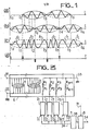
- - la figure 1, représente des chronogrammes de signaux permettant d'expliquer la modulation par déplacement de fréquence à spectre minimal ;
- - la figure 2 est un schéma de principe d'un filtre adapté à une séquence de signaux modulés par déplacement de fréquence à spectre minimal ;
- - la figure 3 est un schéma d'un premier mode de réalisation préféré du dispositif selon l'invention ;
- - la figure 4 est un schéma d'un second mode de réalisation préféré du dispositif selon l'invention
- - la figure 5 est un schéma détaillé d'un élément commun aux figures 3 et 4.
- - Figure 1 shows timing diagrams of signals to explain the modulation by frequency shift at minimum spectrum;
- - Figure 2 is a block diagram of a filter adapted to a sequence of signals modulated by frequency shift at minimum spectrum;
- - Figure 3 is a diagram of a first preferred embodiment of the device according to the invention;
- - Figure 4 is a diagram of a second preferred embodiment of the device according to the invention
- - Figure 5 is a detailed diagram of an element common to Figures 3 and 4.
Les éléments qui se correspondent identiquement d'une figure à l'autre sont désignés par le même repère.The elements which correspond identically from one figure to another are designated by the same reference.
On considère un signal a résultant du produit analogique d'un signal porteur, ayant une fréquence F et d'un signal modulant constitué de demi-cycles de sinusoïde de durée 2 τ , ![]()
- ε1cos2πFct.sin

- ε2sin2πFct.cos2

- ε 1 cos2πF c t.sin
- ε 2 sin2πF c t.cos2
La somme des deux signaux a et b est un signal c dont l'équation est donnée par la relation suivante :
Ce signal somme c est un signal modulé "par déplacement de fréquence à spectre minimal" ayant une variation de phase continue et une amplitude constante. L'expérience montre et le calcul confirme que ces caractéristiques ne sont obtenues qu'à la condition suivante :
ωc.τ = ![]()
cette relation entraîne, entre la fréquence Fc et la pseudo-fréquence f, la relation suivante Fc = (2k+1)f.This sum signal c is a modulated signal "by frequency shift with minimum spectrum" having a continuous phase variation and a constant amplitude. Experience shows and the calculation confirms that these characteristics are only obtained under the following condition:
ω c .τ = ![]()
this relation involves, between the frequency F c and the pseudo-frequency f, the following relation F c = (2k + 1) f.
Sur la figure 1 est représenté un signal a supposé n'exister qu'entre les instants t1 et t5, avec ε1 = 1 entre les instants t1 et t 3 et ε1 = -1 entre les instants t3 et t5 (signal modulant en trait plein); en outre il est à noter que t5 - t3 = t3 - t1 = 2τ. Un tel signal b supposé n'exister qu'entre les instants t2. et t6 est représenté sur la figure 1 avec :
- ε2 = 1 entre les instants to et t2 ;
- ε2 = -1 entre les instants t2 et t4 ;
- E2 = 1 entre les instants t4 et t6 (signal modulant en trait plein) ;
- ε 2 = 1 between the instants t o and t 2 ;
- ε 2 = -1 between times t 2 and t 4 ;
- E2 = 1 between instants t 4 and t 6 (signal modulating in solid lines);
La somme de ces signaux a et b est représentée par le signal c de la figure 1. La fréquence de ce signal c varie de la façon suivante d'une durée τ à l'autre :
- - entre les instants to et t1 : fréquence Fc (partie non significative du message)
- - entre les instants t1 et t2 : fréquence F2 car

- - entre les instants t2 et t3 : fréquence F1 car

- - entre les instants t3 et t4 : fréquence F2 car

- - entre les instants t4 et t5 : fréquence F1 car

- - entre les instants t5 et t6 : fréquence Fc (partie non significative du message)
- - between instants t o and t 1 : frequency F c (non-significant part of the message)
- - between times t 1 and t 2 : frequency F 2 because
- - between times t 2 and t 3 : frequency F 1 because
- - between instants t 3 and t 4 : frequency F 2 because
- - between instants t 4 and t 5 : frequency F 1 because
- - between instants t 5 and t 6 : frequency F c (non-significant part of the message)
Il est à noter que cette alternance des fréquences F1 et F2 est un cas particulier de la figure 1.It should be noted that this alternation of the frequencies F 1 and F 2 is a particular case of FIG. 1.
En outre dans les équations des signaux a et b susmentionnées, le déphasage à l'origine entre le signal porteur et le signal modulant est de ![]()
![]()
La synthèse d'un signal tel que c peut également être réalisée avec un filtre ayant pour réponse impulsionnelle le train d'oscillations de fréquence Fc du signal a pris entre les instants t1 et t3, et recevant sur son entrée le signal d, de la figure 1, constitué d'impulsions brèves de période τ. Une impulsion brève. positive correspond à une valeur de εi (i = 1 ou 2) égale à + 1, et une impulsion brève négative correspond à une valeur de εi égale à - 1.The synthesis of a signal such as c can also be carried out with a filter having as impulse response the train of oscillations of frequency F c of the signal took between the instants t 1 and t 3 , and receiving on its input the signal d, of figure 1, made up of brief pulses of period τ. A brief impulse. positive corresponds to a value of ε i (i = 1 or 2) equal to + 1, and a short negative pulse corresponds to a value of ε i equal to - 1.
Les conditions nécessaires à l'obtention des fréquences F1 et F2 sont alors les suivantes :
- - fréquence F2 si les deux dernières impulsions consécutives sont de même signe
- - fréquence F1 si les deux dernières impulsions consécutives sont de signe contraire.
- - frequency F 2 if the last two consecutive pulses have the same sign
- - frequency F 1 if the last two consecutive pulses are of opposite sign.
En fait, entre les instants t1 et t5, le signal c représente un signal modulé bifréquence dont les deux valeurs de fréquences F1 et F2 peuvent être utilisées pour traduire un code binaire à permutations circulaires.In fact, between the instants t 1 and t 5 , the signal c represents a dual-frequency modulated signal whose two frequency values F 1 and F 2 can be used to translate a binary code with circular permutations.
Le codage binaire à permutations circulaires d'une première information se traduit généralement par une première séquence dans laquelle les bits sont ordonnés d'une façon prédéterminée, cette séquence, appelée "séquence de base" dans ce qui suit, étant séparée de la suiuante par une absence de signal d'une durée donnée.The binary coding with circular permutations of a first item of information generally results in a first sequence in which the bits are ordered in a predetermined manner, this sequence, called "basic sequence" in the following, being separated from the following by an absence of signal of a given duration.
Les autres séquences comportant les informations suivantes, séparées entre elles par une absence de signal, sont obtenues par permutations circulaires de la séquence initiale. Cette modulation par séquences est un cas particulier de la "modulation M-aire", M étant le nombre de permutations circulaires utilisées.The other sequences comprising the following information, separated from one another by an absence of signal, are obtained by circular permutations of the initial sequence. This sequence modulation is a special case of "M-ary modulation", M being the number of circular permutations used.
Chaque séquence de M bits correspond à une information élémentaire à transmettre (par exemple une lettre de l'alphabet); donc avec une "séquence de base" telle que les M séquences, déduites l'une de l'autre par permutation circulaire, ne soient pas identiques, il est possible de transmettre M informations élémentaires différentes.Each sequence of M bits corresponds to elementary information to be transmitted (for example a letter of the alphabet); so with a "basic sequence" such that the M sequences, deduced from each other by circular permutation, are not identical, it is possible to transmit M different elementary information.
On suppose, dans ce qui suit, que les signaux à démoduler ont été obtenus suivant le procédé indiqué plus haut à l'aide d'un filtre ayant pour réponse impulsionnelle le-train d'oscillations du signal a , pris entre les instants t1 et t3. Ce filtre étant appelé ci-après "filtre d'émission".It is assumed, in what follows, that the signals to be demodulated were obtained according to the method indicated above using a filter having as impulse response the oscillation train of the signal a, taken between the instants t 1 and t 3 . This filter is hereinafter called "emission filter".
La démodulation de tels signaux modulés par séquences de permutations par déplacement de fréquence a pour but de restituer une impulsion dont la position dans le temps, à l'intérieur d'un intervalle de durée M.τ est fonction de l'information reçue.The purpose of demodulating such signals modulated by sequences of permutations by frequency displacement is to restore a pulse whose position in time, within a duration interval M.τ is a function of the information received.
Pour identifier une séquence de code connu, l'expérience montre et le calcul confirme qu'il suffit d'utiliser comme démodulateur, un filtre adapté à cette séquence; on entend ici et dans les revendications par filtre adapté à un train d'oscillations de fréquence Fc ou à une séquence telle que définie, un filtre dont la réponse impulsionnelle est l'inverse dans le temps du train ou de la séquence compte non tenu de la phase à l'origine de la fréquence porteuse. Un filtre adapté à un signal de durée finie est celui dont la réponse impulsionnelle est ce même signal inversé dans le temps.To identify a known code sequence, experience shows and the calculation confirms that it suffices to use as a demodulator, a filter adapted to this sequence; here and in the claims is understood by filter adapted to a train of oscillations of frequency F c or to a sequence as defined, a filter whose impulse response is the inverse over time of the train or of the sequence without taking account of the phase at the origin of the carrier frequency. A filter adapted to a signal of finite duration is the one whose impulse response is this same signal inverted over time.
Le principe d'un tel filtre adapté sera exposé à l'aide de la figure suivante.The principle of such a suitable filter will be explained using the following figure.
Sur la figure 2, un filtre 2, recevant la séquence de code connu de n bits sur son entrée 20, alimente par sa sortie 21, n lignes à retard L1 à Ln disposées en série et imposant chacune un retard égal à τ. La sortie 21 du filtre 2 ainsi que la sortie de chaque ligne à retard L1 à Ln sont respectivement reliées aux n+1 entrées d'un dispositif de sommation 3 dont la sortie 22 constitue la sortie du filtre adapté. Il est à noter que chaque entrée du dispositif de sommation 3 inverse ou non le signal qui lui est appliqué pour permettre de réaliser le filtre adapté à la séquence de code connu.In FIG. 2, a
Le fonctionnement de ce dispositif est le suivant.The operation of this device is as follows.
Le filtre 2 présente une réponse impulsionnelle ayant la forme du trains d'oscillations de fréquence Fc, appelé "signal de base" dans ce qui suit, du signal a de la figure 1 pris entre les instants t1 et t3. D'après ce qui a été dit plus haut l'enveloppe de modulation du signal de base étant symétrique dans le temps, le filtre 2 est un filtre adapté à ce signal de base. Il est à noter qu'il est désirable que les filtres 2 du démodulateur et le filtre d'émission doivent être réalisés simultanément par les mêmes masques (en intégration monolithique), afin qu'une dissymétrie accidentelle du filtre d'émission soit reproduite sur le filtre 2. Le filtre 2, recevant la séquence à identifier, fournit un signal qui est reproduit à la sortie de chaque ligne à retard L1 à Ln avec des retards respectifs de valeur τ à nτ. Tous ces signaux de sortie sont sommés algébriquement par le dispositif de sommation 3. Cette sommation algébrique est réalisée suivant un code inversé dans le temps du code d'émission (signaux e1 et ε2) de la séquence émise (par exemple un code inverse dans le temps de celui du signal d de la figure 1 si la séquence reçue est celle de ce signal). Ce démodulateur constitue donc un filtre adapté à cette séquence à identifier.The
L'expérience montre et le calcul confirme que le signal de sortie d'un tel filtre adapté à une séquence donnée présente pour cette séquence un maximum d'amplitude supérieur aux maxima d'amplitude qu'il peut présenter pour les autres séquences du même code.Experience shows and the calculation confirms that the output signal of such a filter adapted to a given sequence has for this sequence a maximum amplitude greater than the amplitude maxima that it can present for the other sequences of the same code.
Le principe du démodulateur suivant l'invention consiste à adjoindre à un filtre adapté à une séquence dite "d'accord", normalement la "séquence de base", un dispositif de répétition en un point ou un autre de ce filtre permettant d'obtenir du démodulateur, pour une séquence reçue, la même réponse que s'il l'avait reçue deux fois de suite.The principle of the demodulator according to the invention consists in adding to a filter suitable for a sequence known as "tuning", normally the "basic sequence", a device for repeating at one point or another of this filter making it possible to obtain from the demodulator, for a sequence received, the same response as if it had received it twice in a row.
Il est aisé de vérifier qu'à un moment donné on trouvera dans la réponse totale du démodulateur un signal identique à la réponse du filtre adapté à sa "séquence d'accord", et que l'instant ou apparaîtra le ma-. ximum correspondant sera fonction de la séquence reçue.It is easy to verify that at a given moment in the total response of the demodulator will be found a signal identical to the response of the filter adapted to its "chord sequence", and that the instant when the ma- will appear . The corresponding maximum will depend on the sequence received.
Dans ce premier mode de réalisation illustré par la figure 3 on utilise un filtre à ondes acoustiques de surface comportant deux transducteurs d'entrée couplés à un même transducteur de sortie, et dont chacun forme avec le transducteur de sortie un filtre tel que le filtre 2 de la figure 2, la différence de parcours de l'onde acoustique entre la sortie des deux transducteurs d'entrée constituant le dispositif de répétition.In this first embodiment illustrated in FIG. 3, a surface acoustic wave filter is used comprising two input transducers coupled to the same output transducer, and each of which forms with the output transducer a filter such as
Sur la figure 3, un substrat piézoélectrique de quartz 6 comporte un premier jeu d'électrodes métalliques parallèles, de différentes longueurs et alimentées en parallèle par le signal reçu sur l'entrée 31. Ce substrat 6 comporte également un deuxième jeu d'électrodes métalliques, parallèles entre elles et parallèles aux électrodes du premier jeu, présentant différentes longueurs, et ayant une extrémité reliée à l'entrée 32 par une connexion commune, l'entrée 32 étant elle-même reliée à la masse. Ces deux jeux d'électrodes sont entrelacées et leur zone d'interpénétration est symbolisée par le pourtour 4 en pointillé (correspondant à la forme de la réponse impulsionnelle du filtre). Le substrat 6 comporte également un troisième et un quatrième jeux d'électrodes identiques et parallèles aux précédents, également reliés aux entrées 31 et 32 (ayant un pourtour d'interpénétration 5), et décalés des précédents d'une distance donnée correspondant au temps de propagation T = n τ, de l'onde acoustique de surface, dans le substrat 6.In FIG. 3, a
Le substrat 6 comporte un cinquième jeu d'électrodes métalliques e1 à en+1, parallèles entre elles et parallèles aux électrodes du deuxième jeu, présentant des longueurs égales ayant une extrémité reliée à la sortie 33 par une connexion commune, la sortie 33 étant elle-même reliée à la masse. Ce substrat comporte également un sixième jeu d'électrodes métalliques e'1 à e' n+1, toutes de même longueur, parallèles entre elles et parallèles aux électrodes du cinquième jeu. Ces cinquième et sixième jeux d'électrodes sont entrelacés, et ont leurs électrodes e'1 à e'n+1 respectivement très proches des électrodes e1 à en+1 mais espacées entre elles d'une distance donnée 1, telle que
Les signaux logiques T1 à Tn+1. permettent de commander les commutateurs I1 à In+1 pour relier respectivement les électrodes e'1 à e'n+1 à l'entrée 35 si leur état logique est à l'état "1" et à l'entrée 36 si leur état logique est à l'état "O".Logic signals T 1 to T n + 1 . allow the switches I 1 to I n + 1 to be controlled to connect the electrodes e ' 1 to e' n + 1 respectively to input 35 if their logic state is in state "1" and to input 36 if their logical state is in state "O".
Ce dispositif de démodulation a été réalisé pour une fréquence Fc de 68,75 MHz, une valeur de T de 200 ns et pour n = 32.This demodulation device was produced for a frequency F c of 68.75 MHz, a value of T of 200 ns and for n = 32.
Le fonctionnement de ce dispositif est le suivant.The operation of this device is as follows.
L'ensemble des premier et deuxième jeux d'électrodes constitue un transducteur d'entrée qui, par effet piézoélectrique, convertit les signaux électriques reçus sur l'entrée 31 en une onde acoustique de surface de forme identique à la réponse électrique de ce transducteur. L'ensemble des troisième et quatrième jeux d'électrodes constitue un transducteur de sortie qui reçoit cette onde et la transforme, par effet piézoélectrique inverse, en un signal électrique (Proceeding of the IEEE, May 1976, Vol. 64, n° 5, pages 581 à 595) de forme identique à celle de l'onde acoustique de surface.The set of first and second sets of electrodes constitutes an input transducer which, by piezoelectric effect, converts the electrical signals received on the
En outre l'ensemble des premier et deuxième jeux d'électrodes ainsi que les troisième et quatrième jeux d'électrodes constituent chacun un filtre ayant pour réponse impulsionnelle un train d'oscillations de fréquence Fc dont l'enveloppe est donnée par le pourtour 4 de la figure 3 (Proceeding of the IEEE, May 1976, vol. 64, n° 5, pages 639 à 651). Ces ensembles constituent donc respectivement deux filtres tels que le filtre 2 de la figure 2, et la distance entre les entrées permet de répéter la séquence reçue.In addition, all of the first and second sets of electrodes as well as the third and fourth sets of electrodes each constitute a filter having for impulse response a train of oscillations of frequency F c , the envelope of which is given by the periphery 4 of FIG. 3 (Proceeding of the IEEE, May 1976, vol. 64, n ° 5, pages 639 to 651). These assemblies therefore respectively constitute two filters such as
De même l'ensemble des troisième et quatrième jeux d'électrodes est identique à une ligne à retard comportant n retards élémentaires de valeur τ. Cette ligne à retard est donc identique aux n lignes à retard de la figure 2.Likewise, the set of third and fourth sets of electrodes is identical to a delay line comprising n elementary delays of value τ. This delay line is therefore identical to the n delay lines in FIG. 2.
Les commutateurs I1 à In+1 permettent de réaliser le codage de cette partie du démodulateur, suivant l'inverse dans le temps du code de la "séquence de base", qui sera appelé "code d'accord" dans ce qui suit (ce codage était réalisé par les entrées du dispositif de sommation 3 de la figure 2 pour un code fixe et connu).The switches I 1 to I n + 1 make it possible to code this part of the demodulator, according to the inverse in time of the code of the "basic sequence", which will be called "chord code" in the following (this coding was carried out by the inputs of the summing device 3 of FIG. 2 for a fixed and known code).
Le fonctionnement de ce dispositif est le suivant.The operation of this device is as follows.
Le codage du démodulateur (en "code d'accord") est réalisé par l'état logique des signaux T1 à Tn+1.The coding of the demodulator (in "agreement code") is carried out by the logic state of the signals T 1 to T n + 1 .
Lorsque l'entrée 31 reçoit, à un instant t', une séquence déduite de la séquence de base par permutations circulaires et correspondant à une information donnée, cette séquence est transférée du transducteur d'entrée ayant le pourtour d'interpénétration 5 sur les n+1 der- nièrespaires d'électrodes e1, e'1 à en+1, e'n+1 du transducteur de sortie, avec un retard θ (θ étant le temps de propagation, dans le substrat 6, entre les transducteurs d'entrée et de sortie). En général l'amplitude maximale ne sera pas encore obtenue du fait de la non coïncidence de la séquence reçue avec la séquence d'accord (filtre non adapté à la séquence reçue). La séquence reçue par le transducteur d'entrée ayant le pourtour d'interpénétration 4 sera fournie aux électrodes du transducteur de sortie au fur et à mesure que la séquence fournie par le précédent transducteur d'entrée (ayant le pourtour d'interpénétration 5) quitte les électrodes du transducteur de sortie, du fait que la distance séparant les deux transducteurs d'entrée correspond à un retard T = nτ. A un instant donné la séquence présente sur les électrodes du transducteur de sortie, et due à la somme des informations partielles provenant des deux transducteurs d'entrée, coïncidera avec la séquence d'accord; à cet instant apparaîtra l'amplitude maximale susmentionnée. Ensuite les informations continuent à se propager d'une paire d'électrodes à la suivante. Il est à noter que la durée de propagation des informations sur ces paires d'électrodes, pendant laquelle la sortie du sommateur algébrique 7 est susceptible de délivrer un signal,est de 3n τ.When the
Il est en outre à noter que cette amplitude maximale sera en général accompagnée de deux maxima d'amplitude inférieure ou égale, ces maxima étant dus au fait que l'information contenue sur les électrodes du transducteur de sortie coïncide partiellement avec la "séquence d'accord". Ces deux maxima seront situés, temporellement, de part et d'autre de l'amplitude maximale. D'où la nécessité d'un dispositif permettant de sélectionner l'amplitude maximale dont la position temporelle traduit l'information utile contenue dans la séquence reçue. Cette amplitude maximale ne peut être obtenue qu'entre les instants t'+nτ +θ et t'+2nτ+θ si t' est l'instant de début de réception (correspondant à l'instant t du signal c de la figure 1) de la séquence ; on a supposé dans ce qui précède que lors de l'émission on ait supprimé (à l'aide d'un interrupteur commandé et disposé en série sur la ligne de -signal) les parties du signal correspondant à celles du signal c de la figure 1 comprises entre les instants to et t1 d'une part et t5 et t6 d'autre part.It should also be noted that this maximum amplitude will generally be accompanied by two maxima of less or equal amplitude, these maxima being due to the fact that the information contained on the electrodes of the output transducer partially coincides with the "sequence of agreement". These two maxima will be located, temporally, on either side of the maximum amplitude. Hence the need for a device making it possible to select the maximum amplitude whose temporal position translates the useful information contained in the received sequence. This maximum amplitude can only be obtained between the instants t '+ nτ + θ and t' + 2nτ + θ if t 'is the reception start time (corresponding to the instant t of the signal c of the fi gure 1) of the sequence; it has been assumed in the foregoing that during transmission, the parts of the signal corresponding to those of signal c in the figure have been deleted (using a controlled switch arranged in series on the signal line) 1 between the instants t o and t 1 on the one hand and t 5 and t 6 on the other hand.
Le dispositif permettant de sélectionner et d'exploiter l'amplitude maximale est le dispositif de sélection 8 de la figure 3 qui sera étudié en détail sur la figure 5.The device making it possible to select and exploit the maximum amplitude is the selection device 8 of FIG. 3 which will be studied in detail in FIG. 5.
Il est à noter que la séquence d'accord n'est pas nécessairement la "séquence de base", et que si on ne désire pas avoir la possibilité de modifier la "séquence d'accord" les commutateurs I1 à In+1 peuvent être supprimés et le sommateur algébrique 7 remplacé par un simple additionneur. Dans ce cas le codage du démodulateur est réalisé au niveau du transducteur de sortie en plaçant les électrodes ei (1≤i≤n+1) en amont ou en aval des électrodes correspondantes e'i (par rapport à la direction de propagation de l'onde acoustique de surface) suivant que l'on désire une pondération par +1 ou par -1.It should be noted that the chord sequence is not necessarily the "basic sequence", and that if one does not wish to have the possibility of modifying the "chord sequence" the switches I 1 to I n + 1 can be deleted and the
Dans un second mode de réalisation, illustré par la figure 4, le dispositif de répétition est disposé en amont d'un filtre tel que le filtre 2 de la figure 2.In a second embodiment, illustrated by FIG. 4, the repeating device is arranged upstream of a filter such as the
Sur la figure 4, une première entrée 37 d'un sommateur 9 est reliée à une électrode t1 et à l'entrée 31 du dispositif de démodulation. Une seconde entrée de ce sommateur 9 est reliée à une électrode t2 et sa sortie est reliée à un transducteur d'entrée identique à celui de la figure 3 (pourtour d'interpénétration 5). Une paire d'électrodes t1, t'1 (t'1 étant très proche de l'électrode t1 et étant reliée à la masse) est assa- ciée à une paire d'électrodes t2, t'2 (t'2 étant très proche de l'électrode t2 et étant reliée à la masse). La distance entre ces paires d'électrodes constitue une ligne à retard imposant au signal reçu sur l'entrée 31 un retard égal à T = n τ (même retard que celui de la figure 3). Les électrodes e 1 à e n+1 et e'1 à e'n+1, les commutateurs I1 à In+1, le sommateur algébrique 7, le dispositif de sélection 8 ainsi que le substrat 6 sont identiques à ceux de la figure 3 et connectés entre eux de la même façon.In FIG. 4, a
Le fonctionnement de ce dispositif se déduit du fonctionnement du dispositif de la figure 3.The operation of this device is deduced from the operation of the device of FIG. 3.
En effet lorsque l'entrée 31 reçoit, à un instant t', une séquence, cette séquence est transférée à la première paire d'électrodes du transducteur de sortie avec un retard 8 (θ étant le temps de propagation dans le substrat 6 entre les transducteurs d'entrée et de sortie). Une seconde séquence identique à la. précédente mais décalée d'un retard T = n τ sera progressivement appliquée sur les électrodes du transducteur de sortie comme pour le dispositif de la figure 3 (du fait de la ligne à retard constituée des paires d'électrodes t1, t'1 et t2, ti 2 et du sommateur 9).Indeed, when the
Le schéma détaillé du dispositif de sélection 8 des figures 3 et 4 est donné par la figure suivante.The detailed diagram of the selection device 8 of Figures 3 and 4 is given by the following figure.
Sur la figure 5 l'entrée (+) d'un comparateur analogique 11 est reliée à la borne 38, à travers un circuit de détection 10, l'entrée (-) de ce comparateur 11 est reliée à une tension de seuil VS, et la sortie du comparateur 11 est reliée à une première entrée d'une porte ET, 12, ayant une seconde entrée reliée à la sortie d'une ligne à retard 14. La sortie de la porte ET, 12, est reliée à une entrée "horloge" d'un registre à décalage 13 ayant cinq étages et ayant une sortie 34 constituant la sortie du dispositif. Un compteur binaire 15, ayant cinq étages, reçoit sur une entrée 40 un signal d'horloge H de période τ, et comporte une entrée 39 qui est reliée à l'entrée 31 recevant le signal à démoduler, à travers la ligne à retard' 14 imposant à ce signal un retard T = nτ+θ. Les sorties des cinq étages du compteur 15 sont respectivement reliées aux cinq entrées respectives des cinq étages du registre à décalage 13.In FIG. 5, the input (+) of an
Le fonctionnement de ce dispositif est le suivant.The operation of this device is as follows.
Le signal reçu par le circuit de détection 10 est le signal de sortie du sommateur algébrique 7 (figures 3 et 4). Ce signal, décrit précédemment lors de l'étude de la figure 3, a une durée de 3n τ(car le début et la fin de la séquence reçue ne comporte pas de signal à la fréquence F ) et comporte l'impulsion maximale utile entre les instants t' + n τ + θ et t' + 2n τ + 8 si t' est.le début de récaption de la séquence. Le circuit de détection 10 et son filtre passe bas associé (non représenté) permet de fournir à l'entrée (+) du comparateur 11 la courbe enveloppe positive du signal reçu sur la borne 38.The signal received by the
Le comparateur 11 fournit sur sa sortie un état "1" logique lorsque l'amplitude du signal reçu sur son entrée (+) est supérieure à la tension de seuil VS et un état "0" logique dans le cas contraire. Le signal de sortie de ce comparateur 11 peut donc être à l'état "1" pour l'amplitude maximale utile, mais également pour les deux maxima d'amplitude situés dans le premier et le dernier tiers de la durée 3n τ du signal reçu sur la borne 38. La ligne à retard 14 et le compteur 15 associés à la porte ET, 12, permettent de sélectionner l'amplitude maximale utile.The
Le signal de sortie de la ligne à retard (donc sur la deuxième entrée de la porte ET, 12, et sur l'entrée 39 du compteur 15) est à l'état "1" logique à l'ins-- tant t' + n τ + 9. Cet état "1" logique débloque le compteur 15 qui compte de 0 à 31 pendant une durée n τ (durée de la séquence reçue) au rythme de son horloge de période T , et permet d'ouvrir la porte ET, 12 et ainsi de sélectionner l'amplitude maximale utile. Le signal de sortie de la porte ET, 12, est donc à l'état "1" logique pendant la période τ de comptage correspondant à la position dans le temps de l'amplitude maxi- màle utile. Cet état "1" logique permet alors au registre à décalage 13 d'enregistrer l'état du compteur. Le contenu de ce registre est ensuite lu sous forme série sur sa sortie 34.The output signal of the delay line (therefore on the second input of the AND gate, 12, and on the
L'invention n'est pas limitée aux modes de réalisation décrits et représentés, en particulier les dispositifs de démodulation selon l'invention peuvent être réalisés selon les variantes suivantes.The invention is not limited to the embodiments described and shown, in particular the demodulation devices according to the invention can be produced according to the following variants.
Les pourtours 4 et 5 des zones d'interpénétration des premier et deuxième jeux d'électrodes sont identiques au signal, a (de la figure 1) pris entre les instants t1 et t3, mais avec une courbe enveloppe qui n'est plus constituée d'un demi-cycle de sinusoïde mais d'un cycle d'un signal quasi-sinusoïdal à dérivées continues jusqu'à un ordre indéterminé, si tel est le cas pour le filtre d'émission.The
Les lignes à retard imposant au signal d'entrée un retard T = n τ sont des lignes à retard à dispositif à transfert de charges.The delay lines imposing a delay T = n τ on the input signal are delay lines with charge transfer device.
Dans une autre réalisation le substrat 6 peut être du niobate de lithium ou tout autre matériau ayant des propriétés piézoélectriques.In another embodiment the
De tels dispositifs de démodulation sont notamment utilisables dans les systèmes de transmission d'informations analogiques ou numériques codées.Such demodulation devices can be used in particular in coded analog or digital information transmission systems.
Claims (9)
Applications Claiming Priority (2)
| Application Number | Priority Date | Filing Date | Title |
|---|---|---|---|
| FR7820809A FR2431229A1 (en) | 1978-07-12 | 1978-07-12 | DEVICE FOR DEMODULATION OF FREQUENCY-SHIFTED MODULATED SIGNALS AND TRANSMISSION SYSTEM INCLUDING SUCH A DEVICE |
| FR7820809 | 1978-07-12 |
Publications (2)
| Publication Number | Publication Date |
|---|---|
| EP0007276A1 true EP0007276A1 (en) | 1980-01-23 |
| EP0007276B1 EP0007276B1 (en) | 1982-09-15 |
Family
ID=9210670
Family Applications (1)
| Application Number | Title | Priority Date | Filing Date |
|---|---|---|---|
| EP79400481A Expired EP0007276B1 (en) | 1978-07-12 | 1979-07-10 | Demodulation device for frequency shift keyed signals |
Country Status (4)
| Country | Link |
|---|---|
| US (1) | US4382232A (en) |
| EP (1) | EP0007276B1 (en) |
| DE (1) | DE2963673D1 (en) |
| FR (1) | FR2431229A1 (en) |
Families Citing this family (8)
| Publication number | Priority date | Publication date | Assignee | Title |
|---|---|---|---|---|
| US4635221A (en) * | 1985-01-18 | 1987-01-06 | Allied Corporation | Frequency multiplexed convolver communication system |
| FR2738383B1 (en) * | 1995-09-05 | 1997-10-03 | Thomson Csf | METHOD FOR VECTOR QUANTIFICATION OF LOW FLOW VOCODERS |
| FR2778041A1 (en) * | 1998-04-24 | 1999-10-29 | Thomson Csf | Power transmitter tube dynamic compensation method |
| FR2788390B1 (en) | 1999-01-12 | 2003-05-30 | Thomson Csf | HIGH EFFICIENCY SHORTWAVE BROADCAST TRANSMITTER OPTIMIZED FOR DIGITAL TYPE TRANSMISSIONS |
| FR2790343B1 (en) | 1999-02-26 | 2001-06-01 | Thomson Csf | SYSTEM FOR ESTIMATING THE COMPLEX GAIN OF A TRANSMISSION CHANNEL |
| FR2799592B1 (en) | 1999-10-12 | 2003-09-26 | Thomson Csf | SIMPLE AND SYSTEMATIC CONSTRUCTION AND CODING METHOD OF LDPC CODES |
| FR2854994B1 (en) * | 2003-05-16 | 2005-07-01 | Thales Sa | DEVICE AND METHOD FOR SELF-ADAPTIVE INTERFERENCE REJECTION |
| KR100698288B1 (en) * | 2005-02-04 | 2007-03-22 | 삼성전자주식회사 | Programmable Surface Acoustic Wave filter |
Citations (1)
| Publication number | Priority date | Publication date | Assignee | Title |
|---|---|---|---|---|
| US3691464A (en) * | 1968-11-25 | 1972-09-12 | Technical Communications Corp | Asynchronous, swept frequency communication system |
Family Cites Families (4)
| Publication number | Priority date | Publication date | Assignee | Title |
|---|---|---|---|---|
| NL146999B (en) * | 1967-04-18 | 1975-08-15 | Matsushita Electric Ind Co Ltd | DECODER FOR STEREOPHONIC SIGNALS. |
| US3736587A (en) * | 1971-05-26 | 1973-05-29 | Us Air Force | Coherent frequency hopped, phase modulated acoustic surface wave generator |
| FR2167405B1 (en) * | 1972-01-14 | 1976-06-11 | Thomson Csf | |
| FR2246112B1 (en) * | 1973-08-21 | 1978-03-17 | Thomson Csf |
-
1978
- 1978-07-12 FR FR7820809A patent/FR2431229A1/en active Granted
-
1979
- 1979-07-10 DE DE7979400481T patent/DE2963673D1/en not_active Expired
- 1979-07-10 EP EP79400481A patent/EP0007276B1/en not_active Expired
-
1981
- 1981-08-12 US US06/292,338 patent/US4382232A/en not_active Expired - Fee Related
Patent Citations (1)
| Publication number | Priority date | Publication date | Assignee | Title |
|---|---|---|---|---|
| US3691464A (en) * | 1968-11-25 | 1972-09-12 | Technical Communications Corp | Asynchronous, swept frequency communication system |
Non-Patent Citations (3)
| Title |
|---|
| ALTA FREQUENZA, vol. 43, no. 10, Octobre 1974, Milan, IT. C. ATZENI et al. "Design of surface acoustic wave filters", pages 601E-865 a 611E-875. * Page 609E-873, colonne de gauche, lignes 13 a 29 * * |
| PROCEEDINGS OF THE IEEE, vol. 64, no. 5, Mai 1976 New York USA D.P. MORGAN et al. "Spread-spectrum synchronizer using a SAW convolver and recirculation loop", pages 751-753. * Page 751, colonne de droite, lignes 1 a 16 * * |
| WAVE ELECTRONICS, vol. 1, no. 5-6, Juin 1976 Amsterdam, NL. J.H. COLLINS et al. "Application of surface acoustic wave devices to spread spectrum communications" pages 311-342. * Page 322, dernier alinea a page 323, premiere ligne * * |
Also Published As
| Publication number | Publication date |
|---|---|
| FR2431229B1 (en) | 1981-06-26 |
| EP0007276B1 (en) | 1982-09-15 |
| FR2431229A1 (en) | 1980-02-08 |
| DE2963673D1 (en) | 1982-11-04 |
| US4382232A (en) | 1983-05-03 |
Similar Documents
| Publication | Publication Date | Title |
|---|---|---|
| US5048058A (en) | MSK modulation and differentially coherent detection transmission system | |
| EP0194902B1 (en) | Method and system for spread spectrum transmission, especially for information transmission in an electric power distribution network | |
| EP0013343B1 (en) | Process and device to detect a pseudo-random sequence of 0 degree and 180 degree phase changes of the carrier in a data receiver | |
| EP0125979B1 (en) | Demodulator for constant envelope and continuous phase signals angularly modulated by a series of binary symbols | |
| EP0117596B1 (en) | Method of reducing the convergence time of an echo canceller, and device for performing this method | |
| EP0007276B1 (en) | Demodulation device for frequency shift keyed signals | |
| CA1170772A (en) | Method and device for encoding binary data | |
| EP0242912A1 (en) | Device for detecting and discriminating phase shifts in a periodical signal, and use in a telephonic tone signal with phase inversions | |
| EP0018242B1 (en) | Method and device for stochastic demodulation of phase-shift keyed signals working in time division on several channels | |
| EP0352159B1 (en) | Frequency drift tolerant method and device for demodulating constant envelope and continuous phase signals angularly modulated by a series of binary symbols | |
| EP0080544B1 (en) | Method for receiving a data signal with double side-band quadrature carrier modulation | |
| EP0138727B1 (en) | Receiving circuit for a wave modulated at one time in frequency by an analogue signal, at another time in phase by a digital signal | |
| FR2559006A1 (en) | CODING-DECODING DEVICE OF A BINARY DIGITAL SIGNAL TRAIN FOR FOUR-PHASE "OQPSK" DIGITAL MODULATOR-DEMODULATOR | |
| FR2503498A1 (en) | TRANSMITTER FOR ANGULAR-MODULATING SIGNALS | |
| US4109100A (en) | Reverberation compensating communication system | |
| EP0092474B1 (en) | Demodulation filter for a binary frequency-modulated signal | |
| Nanayakkara et al. | High speed receiver designs based on surface acoustic wave devices | |
| JP2570293B2 (en) | Ultrasound modulator / demodulator | |
| JPH09153754A (en) | Saw(surface accoustic wave) converter, saw convolver receiver and communication system using the converter | |
| EP0246135B1 (en) | Phase frequency detector and its use in a phase-locked loop | |
| EP0094040A2 (en) | System for synchronous data transmission with the aid of a constant envelope amplitude-modulated carrier | |
| EP1105978B1 (en) | Method for simultaneously measuring the propagating characteristics of a plurality of radioelectric channels | |
| EP0021943A1 (en) | Microwave digital data transmission system | |
| EP0035434A1 (en) | Transmitting and receiving device for the transmission of digital signals | |
| Ananasso | Review of saw devices and their signal processing applications in space communications |
Legal Events
| Date | Code | Title | Description |
|---|---|---|---|
| PUAI | Public reference made under article 153(3) epc to a published international application that has entered the european phase |
Free format text: ORIGINAL CODE: 0009012 |
|
| AK | Designated contracting states |
Designated state(s): BE CH DE GB IT NL SE |
|
| 17P | Request for examination filed | ||
| ITF | It: translation for a ep patent filed |
Owner name: JACOBACCI & PERANI S.P.A. |
|
| GRAA | (expected) grant |
Free format text: ORIGINAL CODE: 0009210 |
|
| AK | Designated contracting states |
Designated state(s): BE CH DE GB IT NL SE |
|
| REF | Corresponds to: |
Ref document number: 2963673 Country of ref document: DE Date of ref document: 19821104 |
|
| PGFP | Annual fee paid to national office [announced via postgrant information from national office to epo] |
Ref country code: CH Payment date: 19830629 Year of fee payment: 5 |
|
| PGFP | Annual fee paid to national office [announced via postgrant information from national office to epo] |
Ref country code: SE Payment date: 19830630 Year of fee payment: 5 Ref country code: BE Payment date: 19830630 Year of fee payment: 5 |
|
| PGFP | Annual fee paid to national office [announced via postgrant information from national office to epo] |
Ref country code: NL Payment date: 19830722 Year of fee payment: 5 |
|
| PG25 | Lapsed in a contracting state [announced via postgrant information from national office to epo] |
Ref country code: SE Effective date: 19840711 |
|
| PG25 | Lapsed in a contracting state [announced via postgrant information from national office to epo] |
Ref country code: CH Effective date: 19840731 Ref country code: BE Effective date: 19840731 |
|
| BERE | Be: lapsed |
Owner name: THOMSON-CSF Effective date: 19840710 |
|
| PG25 | Lapsed in a contracting state [announced via postgrant information from national office to epo] |
Ref country code: NL Effective date: 19850201 |
|
| NLV4 | Nl: lapsed or anulled due to non-payment of the annual fee | ||
| REG | Reference to a national code |
Ref country code: CH Ref legal event code: PL |
|
| REG | Reference to a national code |
Ref country code: GB Ref legal event code: 746 |
|
| PGFP | Annual fee paid to national office [announced via postgrant information from national office to epo] |
Ref country code: DE Payment date: 19910624 Year of fee payment: 13 |
|
| PGFP | Annual fee paid to national office [announced via postgrant information from national office to epo] |
Ref country code: GB Payment date: 19910625 Year of fee payment: 13 |
|
| PG25 | Lapsed in a contracting state [announced via postgrant information from national office to epo] |
Ref country code: GB Effective date: 19920710 |
|
| GBPC | Gb: european patent ceased through non-payment of renewal fee |
Effective date: 19920710 |
|
| PG25 | Lapsed in a contracting state [announced via postgrant information from national office to epo] |
Ref country code: DE Effective date: 19930401 |
|
| EUG | Se: european patent has lapsed |
Ref document number: 79400481.2 Effective date: 19850612 |
|
| PLBE | No opposition filed within time limit |
Free format text: ORIGINAL CODE: 0009261 |
|
| STAA | Information on the status of an ep patent application or granted ep patent |
Free format text: STATUS: NO OPPOSITION FILED WITHIN TIME LIMIT |