EP0016629A2 - System and method for restoring image signal levels and setting signal gain for image-viewing devices - Google Patents
System and method for restoring image signal levels and setting signal gain for image-viewing devices Download PDFInfo
- Publication number
- EP0016629A2 EP0016629A2 EP80300824A EP80300824A EP0016629A2 EP 0016629 A2 EP0016629 A2 EP 0016629A2 EP 80300824 A EP80300824 A EP 80300824A EP 80300824 A EP80300824 A EP 80300824A EP 0016629 A2 EP0016629 A2 EP 0016629A2
- Authority
- EP
- European Patent Office
- Prior art keywords
- signals
- image
- signal
- image signals
- dark
- Prior art date
- Legal status (The legal status is an assumption and is not a legal conclusion. Google has not performed a legal analysis and makes no representation as to the accuracy of the status listed.)
- Granted
Links
Images
Classifications
-
- H—ELECTRICITY
- H04—ELECTRIC COMMUNICATION TECHNIQUE
- H04N—PICTORIAL COMMUNICATION, e.g. TELEVISION
- H04N25/00—Circuitry of solid-state image sensors [SSIS]; Control thereof
- H04N25/60—Noise processing, e.g. detecting, correcting, reducing or removing noise
- H04N25/63—Noise processing, e.g. detecting, correcting, reducing or removing noise applied to dark current
-
- H—ELECTRICITY
- H04—ELECTRIC COMMUNICATION TECHNIQUE
- H04N—PICTORIAL COMMUNICATION, e.g. TELEVISION
- H04N25/00—Circuitry of solid-state image sensors [SSIS]; Control thereof
-
- H—ELECTRICITY
- H04—ELECTRIC COMMUNICATION TECHNIQUE
- H04N—PICTORIAL COMMUNICATION, e.g. TELEVISION
- H04N25/00—Circuitry of solid-state image sensors [SSIS]; Control thereof
- H04N25/70—SSIS architectures; Circuits associated therewith
- H04N25/701—Line sensors
Definitions
- This invention relates to a system and method for restoring image signal levels and setting signal gain for image-viewing devices in response to prevailing operating conditions.
- the output signals produced by the CCDs include an image potential proportional to the intensity of the image portion viewed by the array photosensitive elements and a potential, referred to as an offset potential, attributable to the inherent operating characteristics "of. the CCD.
- the CCD includes an output register for receiving the signals pending output from the CCD and clock means for driving the register to output the signals from th- register. To restore the image signal output by the CCD to a true or absolute value, the offset potential derived from the CCD must be removed from the image signals.
- operating systems utilizing CCDs are normally designed for a fixed image signal gain.
- the signal gain may also vary from one CCD to another, and may even vary for the same CCD for different integration rates.
- a system is optimized for a specific CCD operating at a specific speed, of having to redesign or recalibrate the system to accommodate a change in gain due to changes in CCD operating speed or due to replacement of one CCD with another.
- the present invention aims at reducing the output signals by their actual offset potentials to leave pure image signals, and at correcting the amplitude of the output signals to compensate for the actual gain factor to provide image signals at a preset level.
- the present invention is characterised by means for generating 'dark' and 'light' level non-image signals in the output register with a plurality of image signals; means for separating the dark and light signals from the image signals output from the output register; processing means for determining from the dark and light signals an offset potential and a signal gain factor required to bring the image signals to a preset signal level; signal-restoring means for removing the offset potential from succeeding image signals to restore succeeding image signals to a substantially absolute signal level; and gain-correcting means for adjusting the potential level of succeeding image signals in accordance with the gain factor to provide image signals at the preset signal level.
- the invention further relates to the method of image signal restoration and' gain control for an image viewing device, having plural discrete photosensitive elements for generating image signals representative of the intensity of the image viewed by the elements, and a shift register for receiving the image signals, having the steps of:generating preset dark and light level signals to the shift register with each preset block of image signals clocking the shift register to transfer the block of image signals together with the dark and light level signals serially along the shift register to the shift roister output, separating the dark and light level signals from the block of image signals as the signals are output from the shift register, determining from the dark and light level signals the restoration potential required to restore the image signals to an absolute signal level and the gain factor required to produce an image signal output at a predetermined potential level, removing the restoration potential from the next successive block of image signals to restore the image signals to an absolute signal level, and multiplying the image signals by the gain factor to provide image signals at the predetermined potential level.
- the system 10 serves to restore the image signal output of an image viewing device, exemplified herein by charge coupled device 15 (commonly referred to as a CCD), to an absolute level. Further, to provide for a uniform image signal output level whatever the image viewing device used, or whatever the integration period, automatic gain adjustment of the image signal output is provided.
- CCD charge coupled device 15
- charge-coupled image viewing device such as Fairchild Corp. CCD 121-H is described herein, other image viewing devices, as for example a Rudicon Inc. Charge Coupled Photo Diode Device CCPD-1728, may be used instead.
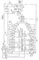
- CCD 15 (Fig. 1) includes a succession or array 11 of photosensitive elements 12 on the narrow center portion of silicon chip 13.
- Array 11 is flanked on either side by rows 14, 16 of transfer gates 21.
- Shift registers 18, 20 which comprise parallel input/serial output analog registers, are disposed on either side of the rows 14, 16 of transfer gates.
- Each transfer gate 21 consists of an electronic switch such as a field-effect transistor (FET), through which the output of the individual photosensitive element 12 is coupled to individual phase gate 23 of shift registers 18, 20.
- FET field-effect transistor
- the total number of transfer gates in each row 14, 16 is equal to one half the total number of photosensitive elements 12 with alternate, i.e. odd-numbered photosensitive elements (12-1, 12-3, ...) coupled through row 14 of transfer gates to shift register 18 and even-numbered photosensitive elements (12-2, 12-4, ...) coupled through row 16 of transfer gates to shift register 20.
- the total number of phase gates 23 in shift registers 18, 20 is equal to the number of photosensitive elements 12 that comprise array 11.
- only alternate shift register phase gates are coupled to photosensitive elements 12.
- an image signal is transferred to phase gates 23-1, 23-3, 23-5, ... of shift register 18 and to phase gates 23-2, 23-4, ... of shift register 20.
- -CCDs 15 serve, in an imaging system of the type shown in U. S. Patent No. 4,122,352 for example, to convert the graphical image of an original document to a series of electronic image signals or 'pixels'.
- photosensitive elements 12 comprise charge coupled cells as in CCD 15
- exposure to the illuminated document generates a charge proportional to the luminous energy reflected from the original document.
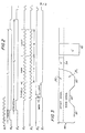
- Exposure is taken over a preset time interval (Ti, Ti' in Figure 2), termed integration time.
- the charges in the cells are transferred en masse to phase gates 23 of shift registers 18, 20 by switches 21 of transfer gate rows 14, 16.
- switches 21 of transfer gate row 14 are enabled by application of clock enabling pulse ⁇ 2 to transfer the charges (i.e., image signals) from the odd-numbered cells to shift register 18 following which switches 21 of transfer gate row 16 are enabled by application of clock enabling pulse ⁇ 3 to transfer the charges from the even numbered cells to shift register 20.
- the integration times, Ti, Ti' are taken between the leading edges of successive transfer clock pulses ⁇ 2, ⁇ 3 for the odd-and even-numbered cells respectively.
- a uniform initial charge, termed offset potential or offset signal herein is provided in shift registers 18, 20.
- a bias Vc is input to gates 67; 68 of CCD 15 from a suitable voltage source, exemplified herein by battery 25..
- the output signals from gate 28 are clocked into holding diode 30 of CCD output amplifier section 31.
- Output amplifier section 31 of CCD 10 includes a current amplifying circuit having cascaded FET pairs 32, 33. Each image signal, which is temporarily held on diode 30, appears at CCD output terminal 35, following amplification by amplifier section 31.
- a typical image signal output 49 from CCD 15 is thereshown.
- Portion 50 of the image signal 49 comprises the offset signal which is derived from the voltage bias Vc.
- Offset signal 50 has its origin in the non-image bearing phase gates of shift registers 18, 20, while introduction of the charges on cells 12 to the remaining phase gates of registers 18, 20 provides the signal 51 proportional to the intensity of the image viewed.
- offset signal 50 and image signal 51 are combined to provide the image signal 49.
- Areas 52, 52' exemplify a dark image area and a light image area respectively. Signals of this type may result for example, in the case where the original document comprises a series of dark lines with light-colored spaces therebetween.
- dark (D) and light (L) signals 54, 55 are dark (D) and light (L) signals 54, 55 respectively.
- signals 54, 55 result from generation of predetermined test or calibration signals in CCD 15.
- the image signals output by CCD 15 include'an offset component.
- the offset component To restore the image signals- to a true or absolute image signal level, i.e., one without an offset component, the offset component must be removed.
- the system gain be constant whatever the CCD used or the integration rate selected.
- Signal gain can vary from CCD to CCD, and with different integration rates.
- the image signals are modified by the application of a compensating gain factor derived from the instantaneous operating characteristics of the CCD in use.
- D dark signals
- L light signals
- Exemplary dark signals (D') and light signals (L') are shown in Figure 3 at 54, 55 respectively.
- the dark and light signals (D,L) generated in CCD 15 are isolated at the CCD output and the dark signals (D) are used to determine the offset component of the image signals while both dark and light signals (D,L) are used to determine the gain factor required to bring the image signals to a predetermined level as will appear.
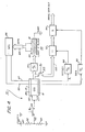
- light signal (L) is derived from a suitable potential source, exemplified herein by battery 60.
- Output lead 61 of battery 60 is tapped by light signal input lead 65 between resistor pair 62, 63.
- battery 60 and resistor pair 62, 63 are chosen to provide the desired voltage level or potential for the light signal (L).
- Input lead 65 is coupled through a. suitable switch such as FET 66 to auxiliary signal input gates 67, 68 of registers 18, 20. As will appear, FET 66 is actuated periodically for a predetermined number of clock pulses, (e.g. 16) to input a series of light signals (L) to CCD registers,18, 20.
- a predetermined number of clock pulses e.g. 16
- L series of light signals
- Dark signal (D) is conveniently obtained by clocking registers 18, 20 a predetermined number of times (e.g. 16) beyond the last image signal. Inasmuch as no intervening exposure takes place, the signal produced in registers 18, 20 has a potential representative of the internal potential of CCD 15, i.e. the CCD offset signal.
- clock pulses ⁇ 6 successively actuate FET 66 to input a series of light signals (L) the level of which is established by battery/resistor combination 60, 62, 63, to shift registers 18, 20.
- blocks 81, 82 of dark and light signals (D, L) are each 16 pulse.s wide.
- the stream of signals output by CCD 15, which are understood to be made up of a relatively large block of image signals (e.g. 1,728 pixels) followed by the relatively small (e.g. 16 pixels each) blocks 81, 82 of dark and light signals (D, L) are input to Analog-to-Digital (hereinafter A/D) converter 84 where the analog signals are converted to digital signals.
- A/D converter is a TRW Model TDC 10145 converter.
- Digital image signals from converter 84 are input to serial in/parallel out buffer 85.
- One suitable buffer is buffer Model No. 74Sl95 by TRW, Inc.
- buffer 85 need only be wide enough to handle the dark (D) and light (L) signals.
- buffer 85 may comprise a 32 bit buffer. It will be understood that the image signals, which precede the dark ( D ) and light (L) signals pass through buffer 85 and are discarded.
- Block 81 of dark signals (D) and block 82 of light signals (L) in buffer 85 are input to microprocessor MPU 86 through data bus 83.
- Microprocessor 86 which may comprise an Intel Model 8080 MPU by Intel Corp., averages the block of dark signals ( D ) in accordance with the following function:
- the offset signal V(OFF) determined is output by MPU 86 via lead 87 to Digital-to-Analog (D/A herein) converter 88.
- MPU 86 averages the block of light signals (L) in accordance with the following function:
- MPU 86 determines the instantaneous gain multiplicand K in accordance with the following relationship:
- Each succeeding line of signals output by CCD 15 is input via A/D converter 84 to buffer 85 where the dark (D) and light (L) level signals are processed by MPU 86 in the manner described heretofore. As fresh signals enter buffer 85, the previous blocks 81, 82 of dark (D) and light (L) level signals are discarded.
- Image signals in the output of CCD 15 are also placed' on data output bus 100 which carries the image signals to subtractor 92 for processing.
- the offset signal V (OFF) is subtracted from the image signals thereby restoring the image signals to an absolute or substantially-absolute signal level.
- Image signals from subtractor 92 are input to multiplier 94 where the image signals are multiplied by the multiplicand factor K as determined by MPU 86 for the preceding line of image signals. This sets the image signal output level to assure a level commensurate with the ideal output level Vt in accommodation of the particular CCD being used and the existing integration time.
- the image signals are output by multiplier 94 for further processing and/or use.
- FET control gate 103 serves to limit the signal input to data bus 100 to image signals and exclude other signals, particularly dark and light signals (D, L).
- Clock pulse ⁇ 7 actuates gate 103 in unison with the image signal output of CCD 15 to transfer image signals into bus 100. However, actuation of gate 103 is terminated following the last image signal to preclude passage of dark and light signals (D, L) into output bus 100.
- FETs 66, 103 may comprise Signetics Model No. SD5001 FETs.
- blocks 81, 82 of dark (D) and light (L) signals are generated with each line of image signals, other relationships, as for example, generating dark and light signals at the start of each page with calibration .of CCD 15 once per page, may be envisioned.
- dark signals (D) may be derived from a source other than CCD bias source 25, that the potential levels of both the dark and light signals may comprise any suitable potential, and that the order in which dark and light signals are generated may be reversed.
- multiplier 94 is disclosed herein as being downstream of subtractor 92, the positions may be reversed. In that circumstance, suitable compensation must be made for the change in processing locations of the image signals as will be understood.
Abstract
Description
- This invention relates to a system and method for restoring image signal levels and setting signal gain for image-viewing devices in response to prevailing operating conditions.
- In systems employing image viewing devices such as charge-coupled devices(or CCDs)having an array of photosensitive elements for viewing as by raster scanning an original, it is known that the output signals produced by the CCDs include an image potential proportional to the intensity of the image portion viewed by the array photosensitive elements and a potential, referred to as an offset potential, attributable to the inherent operating characteristics "of. the CCD. The CCD includes an output register for receiving the signals pending output from the CCD and clock means for driving the register to output the signals from th- register. To restore the image signal output by the CCD to a true or absolute value, the offset potential derived from the CCD must be removed from the image signals. However, if the offset potential that is removed is greater or less than the actual offset potential, a noticeable aberration or distortion in the image signal may result. And since the operating characteristics of CCDs often vary widely from one CCD to another and even vary for the same CCD for different integration rates, accurately determining the offset potential to be removed is often difficult. The problem is complicated in systems where multiple CCDs are employed.
- Further, operating systems utilizing CCDs are normally designed for a fixed image signal gain. However, it is known that since the operating characteristics of imaging devices such as CCDs may vary, the signal gain may also vary from one CCD to another, and may even vary for the same CCD for different integration rates. Thus one is faced with the prospect, in the case where a system is optimized for a specific CCD operating at a specific speed, of having to redesign or recalibrate the system to accommodate a change in gain due to changes in CCD operating speed or due to replacement of one CCD with another.
- The present invention aims at reducing the output signals by their actual offset potentials to leave pure image signals, and at correcting the amplitude of the output signals to compensate for the actual gain factor to provide image signals at a preset level. Accordingly, the present invention is characterised by means for generating 'dark' and 'light' level non-image signals in the output register with a plurality of image signals; means for separating the dark and light signals from the image signals output from the output register; processing means for determining from the dark and light signals an offset potential and a signal gain factor required to bring the image signals to a preset signal level; signal-restoring means for removing the offset potential from succeeding image signals to restore succeeding image signals to a substantially absolute signal level; and gain-correcting means for adjusting the potential level of succeeding image signals in accordance with the gain factor to provide image signals at the preset signal level.
- The invention further relates to the method of image signal restoration and' gain control for an image viewing device, having plural discrete photosensitive elements for generating image signals representative of the intensity of the image viewed by the elements, and a shift register for receiving the image signals, having the steps of:generating preset dark and light level signals to the shift register with each preset block of image signals clocking the shift register to transfer the block of image signals together with the dark and light level signals serially along the shift register to the shift roister output, separating the dark and light level signals from the block of image signals as the signals are output from the shift register, determining from the dark and light level signals the restoration potential required to restore the image signals to an absolute signal level and the gain factor required to produce an image signal output at a predetermined potential level, removing the restoration potential from the next successive block of image signals to restore the image signals to an absolute signal level, and multiplying the image signals by the gain factor to provide image signals at the predetermined potential level.
- The present invention will now be described in detail, by way of example, with reference to the drawings, in which:
- Figure 1 is a schematic representation of an image viewing- device of the present invention;
- Figure 2 is a timing chart showing the operating timing sequences of the device of Fig. 1;
- Figure 3 represents a typical image signal output of the viewing device shown in Figure 1 including the dark and light level signals produced therein in accordance with the present invention; and
- Figure 4 is a circuit schematic showing details of the signal restoration and gain control of the present invention.
- Referring to the drawings, there is shown the image signal restoration and
gain control system 10 of the present invention. - As will appear, the
system 10 serves to restore the image signal output of an image viewing device, exemplified herein by charge coupled device 15 (commonly referred to as a CCD), to an absolute level. Further, to provide for a uniform image signal output level whatever the image viewing device used, or whatever the integration period, automatic gain adjustment of the image signal output is provided. - While a charge-coupled image viewing device, such as Fairchild Corp. CCD 121-H is described herein, other image viewing devices, as for example a Rudicon Inc. Charge Coupled Photo Diode Device CCPD-1728, may be used instead.
- CCD 15 (Fig. 1) includes a succession or array 11 of
photosensitive elements 12 on the narrow center portion ofsilicon chip 13. Array 11 is flanked on either side byrows transfer gates 21.Shift registers rows - Each
transfer gate 21 consists of an electronic switch such as a field-effect transistor (FET), through which the output of the individualphotosensitive element 12 is coupled toindividual phase gate 23 ofshift registers row photosensitive elements 12 with alternate, i.e. odd-numbered photosensitive elements (12-1, 12-3, ...) coupled throughrow 14 of transfer gates to shiftregister 18 and even-numbered photosensitive elements (12-2, 12-4, ...) coupled throughrow 16 of transfer gates to shiftregister 20. - Preferably, the total number of
phase gates 23 inshift registers photosensitive elements 12 that comprise array 11. As a result, only alternate shift register phase gates are coupled tophotosensitive elements 12. In the exemplary arrangement shown, on activation oftransfer gates 21, an image signal is transferred to phase gates 23-1, 23-3, 23-5, ... ofshift register 18 and to phase gates 23-2, 23-4, ... of shift register 20.-CCDs 15 serve, in an imaging system of the type shown in U. S. Patent No. 4,122,352 for example, to convert the graphical image of an original document to a series of electronic image signals or 'pixels'. Where for examplephotosensitive elements 12 comprise charge coupled cells as inCCD 15, exposure to the illuminated document generates a charge proportional to the luminous energy reflected from the original document. Exposure is taken over a preset time interval (Ti, Ti' in Figure 2), termed integration time. Following integration, the charges in the cells are transferred en masse tophase gates 23 ofshift registers switches 21 oftransfer gate rows switches 21 oftransfer gate row 14 are enabled by application of clock enabling pulse Ø2 to transfer the charges (i.e., image signals) from the odd-numbered cells to shiftregister 18 following which switches 21 oftransfer gate row 16 are enabled by application of clock enabling pulse Ø3 to transfer the charges from the even numbered cells to shiftregister 20. In the exemplary arrangement shown, the integration times, Ti, Ti' are taken between the leading edges of successive transfer clock pulses Ø2, Ø3 for the odd-and even-numbered cells respectively. - A
suitable clock 27, which may for example, comprise a crystal oscillator, provides the various clock timing pulses Ø1 - Ø7 seen in Figure 2. - A uniform initial charge, termed offset potential or offset signal herein is provided in
shift registers gates 67; 68 ofCCD 15 from a suitable voltage source, exemplified herein bybattery 25.. - Following transfer of the charges from the charge coupled cells to alternate gates of
output registers registers 18, 20 (i.e., from left to right in Figure 1) to outputgate 28. Inasmuch asalternating phase gates 23 ofregisters gate 28. The image signals and the offset signals from the matching phase gates of the adjoining register are summed ingate 28. - The output signals from
gate 28 are clocked intoholding diode 30 of CCDoutput amplifier section 31. -
Output amplifier section 31 ofCCD 10 includes a current amplifying circuit having cascadedFET pairs diode 30, appears atCCD output terminal 35, following amplification byamplifier section 31. - The image signal on holding
diode 30, following a predetermined time interval determined by the pulse width of clock pulses Ø1, is discarded with activation of discharge FET 37 by a pulse from clock signal ffl. Activation ofFET 37couples holding diode 30 to a suitable voltage source vialine 38 to cleardiode 30 for the next image output signal. - Referring particularly to Figure 3, a typical
image signal output 49 fromCCD 15 is thereshown.Portion 50 of theimage signal 49 comprises the offset signal which is derived from the voltage bias Vc.Offset signal 50 has its origin in the non-image bearing phase gates ofshift registers cells 12 to the remaining phase gates ofregisters signal 51 proportional to the intensity of the image viewed. Atoutput gate 28,offset signal 50 andimage signal 51 are combined to provide theimage signal 49.Areas 52, 52' exemplify a dark image area and a light image area respectively. Signals of this type may result for example, in the case where the original document comprises a series of dark lines with light-colored spaces therebetween. Also shown in Figure 3 are dark (D) and light (L)signals 54, 55 respectively. As will appear, signals 54, 55 result from generation of predetermined test or calibration signals inCCD 15. - As described, the image signals output by
CCD 15 include'an offset component. To restore the image signals- to a true or absolute image signal level, i.e., one without an offset component, the offset component must be removed. - It is desirable in system design and operation, that the system gain be constant whatever the CCD used or the integration rate selected. Signal gain however, can vary from CCD to CCD, and with different integration rates. To ensure that system gain remains constant despite differences between CCDs and differences in integration rates, the image signals are modified by the application of a compensating gain factor derived from the instantaneous operating characteristics of the CCD in use.
- To determine optimum offset and gain levels for
CCD 15, preset dark signals (D) and light signals (L) are generated inCCD 15 at each integration. Exemplary dark signals (D') and light signals (L') are shown in Figure 3 at 54, 55 respectively. As will appear, the dark and light signals (D,L) generated inCCD 15 are isolated at the CCD output and the dark signals (D) are used to determine the offset component of the image signals while both dark and light signals (D,L) are used to determine the gain factor required to bring the image signals to a predetermined level as will appear. - Referring to Figure 4, light signal (L) is derived from a suitable potential source, exemplified herein by battery 60.
Output lead 61 of battery 60 is tapped by lightsignal input lead 65 betweenresistor pair resistor pair -
Input lead 65 is coupled through a. suitable switch such asFET 66 to auxiliarysignal input gates registers FET 66 is actuated periodically for a predetermined number of clock pulses, (e.g. 16) to input a series of light signals (L) to CCD registers,18, 20. - Dark signal (D) is conveniently obtained by clocking
registers 18, 20 a predetermined number of times (e.g. 16) beyond the last image signal. Inasmuch as no intervening exposure takes place, the signal produced inregisters CCD 15, i.e. the CCD offset signal. - Since both dark signals (D) and light signals (L) are provided at the upstream end of
registers CCD 15 provide a relatively accurate representation of CCD processing conditions. - Referring particularly to Figures 1, 2 and 4, as the image signals are clocked serially along shift registers 18, 20 toward
output gate 28, the endmost gates 23-1, 23-2, 23-3, etc. are progressively emptied of image data. As a result, only the offset signal, which is derived from bias Vc and which forms the basis for deriving the dark signals (D), exists in the empty phase gates. A preset number of clock pulses Ø4, Ø5 (i.e. 16) are used to generate ablock 81 of dark signals (D) inregisters FET 66 to input a series of light signals (L) the level of which is established by battery/resistor combination registers block 82 of light signals (L) inshift registers block 81 of dark signals (D). In the exemplary arrangement shown, blocks 81, 82 of dark and light signals (D, L) are each 16 pulse.s wide. - The stream of signals output by
CCD 15, which are understood to be made up of a relatively large block of image signals ( e.g. 1,728 pixels) followed by the relatively small (e.g. 16 pixels each) blocks 81, 82 of dark and light signals (D, L) are input to Analog-to-Digital (hereinafter A/D) converter 84 where the analog signals are converted to digital signals. One suitable A/D converter is a TRW Model TDC 10145 converter. Digital image signals from converter 84 are input to serial in/parallel outbuffer 85. One suitable buffer is buffer Model No. 74Sl95 by TRW, Inc. Inasmuch as only theblocks buffer 85 may comprise a 32 bit buffer. It will be understood that the image signals, which precede the dark (D) and light (L) signals pass throughbuffer 85 and are discarded. -
Block 81 of dark signals (D) and block 82 of light signals (L) inbuffer 85 are input tomicroprocessor MPU 86 throughdata bus 83.Microprocessor 86, which may comprise an Intel Model 8080 MPU by Intel Corp., averages the block of dark signals (D) in accordance with the following function:
- where,
- V(OFF) is the instantaneous average voltage offset signal (i.e. 50 in Figure 3),
- VD1, VD2' ... VDN are the voltage levels of the individual dark signals that comprise
block 81, and - N is the total number of dark signals in
block 81. In the example discussed, N = 16. - The offset signal V(OFF) determined is output by
MPU 86 vialead 87 to Digital-to-Analog (D/A herein)converter 88. - In a similar manner,
MPU 86 averages the block of light signals (L) in accordance with the following function:
- where
- VL (AVG) is the instantaneous average light signal,
- VL1, VL2 ... VLN are the voltage levels of the individual light signals that comprise
block 82, and - N is the number of light signals in
block 82. In the example discussed, N = 16. - Using offset signal V (OFF) and light signal VL (AVG),
MPU 86 determines the instantaneous gain multiplicand K in accordance with the following relationship:
- where
- VT represents the ideal voltage level output.
- Gain multiplicand K is output by
MPU 86 vialead 89 to D/A converter 90. - D/
A converters - D/
A converters A converters subtractor 92 andmultiplier 94 respectively. One suitable subtractor is National Semi-Conductor Model 0032 Differential Amplifier while a -suitable - multiplier is Motorola Model 1595 Multiplier. - Each succeeding line of signals output by
CCD 15 is input via A/D converter 84 to buffer 85 where the dark (D) and light (L) level signals are processed byMPU 86 in the manner described heretofore. As fresh signals enterbuffer 85, theprevious blocks - Image signals in the output of
CCD 15 are also placed' on data output bus 100 which carries the image signals to subtractor 92 for processing. Insubtractor 92 the offset signal V (OFF), as determined for the preceding line of image signals byMPU 86, is subtracted from the image signals thereby restoring the image signals to an absolute or substantially-absolute signal level. - Image signals from
subtractor 92 are input tomultiplier 94 where the image signals are multiplied by the multiplicand factor K as determined byMPU 86 for the preceding line of image signals. This sets the image signal output level to assure a level commensurate with the ideal output level Vt in accommodation of the particular CCD being used and the existing integration time. The image signals are output bymultiplier 94 for further processing and/or use. -
FET control gate 103 serves to limit the signal input to data bus 100 to image signals and exclude other signals, particularly dark and light signals (D, L). Clock pulse Ø7 actuatesgate 103 in unison with the image signal output ofCCD 15 to transfer image signals into bus 100. However, actuation ofgate 103 is terminated following the last image signal to preclude passage of dark and light signals (D, L) into output bus 100. -
FETs - While in the exemplary arrangement shown, blocks 81, 82 of dark (D) and light (L) signals are generated with each line of image signals, other relationships, as for example, generating dark and light signals at the start of each page with calibration .of
CCD 15 once per page, may be envisioned. It will be further understood that dark signals (D) may be derived from a source other than CCD biassource 25, that the potential levels of both the dark and light signals may comprise any suitable potential, and that the order in which dark and light signals are generated may be reversed. - While
multiplier 94 is disclosed herein as being downstream ofsubtractor 92, the positions may be reversed. In that circumstance, suitable compensation must be made for the change in processing locations of the image signals as will be understood.
Claims (7)
Applications Claiming Priority (2)
| Application Number | Priority Date | Filing Date | Title |
|---|---|---|---|
| US23570 | 1979-03-26 | ||
| US06/023,570 US4216503A (en) | 1979-03-26 | 1979-03-26 | Signal restoration and gain control for image viewing devices |
Publications (3)
| Publication Number | Publication Date |
|---|---|
| EP0016629A2 true EP0016629A2 (en) | 1980-10-01 |
| EP0016629A3 EP0016629A3 (en) | 1980-10-15 |
| EP0016629B1 EP0016629B1 (en) | 1984-03-14 |
Family
ID=21815913
Family Applications (1)
| Application Number | Title | Priority Date | Filing Date |
|---|---|---|---|
| EP80300824A Expired EP0016629B1 (en) | 1979-03-26 | 1980-03-19 | System and method for restoring image signal levels and setting signal gain for image-viewing devices |
Country Status (5)
| Country | Link |
|---|---|
| US (1) | US4216503A (en) |
| EP (1) | EP0016629B1 (en) |
| JP (1) | JPS55130276A (en) |
| CA (1) | CA1132244A (en) |
| DE (1) | DE3066908D1 (en) |
Cited By (6)
| Publication number | Priority date | Publication date | Assignee | Title |
|---|---|---|---|---|
| EP0061491A1 (en) * | 1980-10-06 | 1982-10-06 | Hughes Aircraft Co | Automatic responsivity control for a ccd imager. |
| FR2510279A1 (en) * | 1981-07-23 | 1983-01-28 | Rca Corp | RAM CONTROL SIGNAL PROCESSOR |
| EP0541332A1 (en) * | 1991-11-04 | 1993-05-12 | Xerox Corporation | Architecture for analog and digital image sensor arrays |
| EP0627151A1 (en) * | 1992-02-18 | 1994-12-07 | Neopath, Inc. | Method and apparatus for dynamic correction of microscopic image signals |
| FR2713426A1 (en) * | 1993-12-03 | 1995-06-09 | Sony Corp | Load transfer device. |
| US5612739A (en) * | 1993-03-23 | 1997-03-18 | Sony Corporation | Charge transfer device |
Families Citing this family (73)
| Publication number | Priority date | Publication date | Assignee | Title |
|---|---|---|---|---|
| JPS5650668A (en) * | 1979-09-29 | 1981-05-07 | Sharp Corp | Correcting system for reading output |
| US4351004A (en) * | 1980-01-31 | 1982-09-21 | Texas Instruments Incorporated | CCD Imager |
| US4696533A (en) * | 1981-01-12 | 1987-09-29 | Massachusetts Institute Of Technology | Spatial light modulator |
| US4865427A (en) * | 1981-01-12 | 1989-09-12 | Massachusetts Institute Of Technology | Spatial light modulator |
| EP0060149B1 (en) * | 1981-01-14 | 1984-11-21 | Morton Nadler | Image scanning method and device |
| US4408231A (en) * | 1981-07-31 | 1983-10-04 | International Business Machines Corporation | Method and apparatus for calibrating a linear array scanning system |
| US4635126A (en) * | 1981-12-18 | 1987-01-06 | Canon Kabushiki Kaisha | Image pick-up system |
| US4554460A (en) * | 1982-07-02 | 1985-11-19 | Kollmorgen Technologies Corp. | Photodetector automatic adaptive sensitivity system |
| US4525741A (en) * | 1982-11-03 | 1985-06-25 | Ncr Corporation | Self-adjusting video camera |
| US4745466A (en) * | 1983-03-06 | 1988-05-17 | Canon Kabushiki Kaisha | Digital color image processing apparatus with color masking processing unit addressed by a plurality of multi-bit color component signals using various combinations of the bits of the signals |
| DE3408108A1 (en) * | 1983-03-06 | 1984-09-06 | Canon K.K., Tokio/Tokyo | Image processing device |
| US4578711A (en) * | 1983-12-28 | 1986-03-25 | International Business Machines (Ibm) | Video data signal digitization and correction system |
| US4590505A (en) * | 1984-01-10 | 1986-05-20 | The United States Of America As Represented By The Secretary Of The Air Force | Three dimensional optical receiver having programmable gain sensor stages |
| US4584610A (en) * | 1984-02-16 | 1986-04-22 | Olympus Optical Co., Ltd. | Electronic photographing apparatus |
| JPS60189372A (en) * | 1984-03-08 | 1985-09-26 | Dainippon Screen Mfg Co Ltd | Picture input device |
| US4555732A (en) * | 1984-03-22 | 1985-11-26 | Xerox Corporation | Image sensor correction system |
| US4636980A (en) * | 1984-07-25 | 1987-01-13 | Westinghouse Electric Corp. | Three dimensional optical receiver having programmable gain control |
| JPS6153868A (en) * | 1984-08-24 | 1986-03-17 | Dainippon Screen Mfg Co Ltd | Calibration in picture scan signal processing |
| GB8506050D0 (en) * | 1985-03-08 | 1985-04-11 | Crosfield Electronics Ltd | Operating ccd arrays |
| JPH07108023B2 (en) * | 1985-09-04 | 1995-11-15 | エヌ・ベ−・フイリツプス・フル−イランペンフアブリケン | camera |
| US5771070A (en) | 1985-11-15 | 1998-06-23 | Canon Kabushiki Kaisha | Solid state image pickup apparatus removing noise from the photoelectric converted signal |
| US4914519A (en) * | 1986-09-19 | 1990-04-03 | Canon Kabushiki Kaisha | Apparatus for eliminating noise in a solid-state image pickup device |
| US5737016A (en) * | 1985-11-15 | 1998-04-07 | Canon Kabushiki Kaisha | Solid state image pickup apparatus for reducing noise |
| JPH084127B2 (en) * | 1986-09-30 | 1996-01-17 | キヤノン株式会社 | Photoelectric conversion device |
| GB8606200D0 (en) * | 1986-03-13 | 1986-04-16 | Crosfield Electronics Ltd | Operating radiation sensors |
| JPS62293384A (en) * | 1986-06-11 | 1987-12-19 | Toshiba Corp | Picture input device |
| US4991127A (en) * | 1986-08-28 | 1991-02-05 | Hughes Aircraft Company | Offset and gain correction system for image data processing |
| US4862286A (en) * | 1986-11-14 | 1989-08-29 | Canon Kabushiki Kaisha | Image reading apparatus which adjusts image signals to improve signal balance |
| US5121230A (en) * | 1987-01-19 | 1992-06-09 | Canon Kabushiki Kaisha | Image reading apparatus having adjusting circuits for matching the level of and compensating for fluctuation among a plurality of sensing elements |
| DE3723508C1 (en) * | 1987-07-16 | 1988-11-03 | Fraunhofer Ges Forschung | Circuit arrangement for gray value correction of video signals |
| US4920428A (en) * | 1988-07-08 | 1990-04-24 | Xerox Corporation | Offset, gain and bad pixel correction in electronic scanning arrays |
| US5267053A (en) * | 1988-10-27 | 1993-11-30 | Eastman Kodak Company | Automatic reference control for image scanners |
| US4903144A (en) * | 1988-10-27 | 1990-02-20 | Eastman Kodak Company | Automatic D.C. offset control for image scanners |
| JPH02164184A (en) * | 1988-12-19 | 1990-06-25 | Toshiba Corp | X-ray diagnostic equipment |
| JPH0693768B2 (en) * | 1988-12-27 | 1994-11-16 | 日本電気株式会社 | Imaging signal processor |
| US5008739A (en) * | 1989-02-13 | 1991-04-16 | Eastman Kodak Company | Real-time digital processor for producing full resolution color signals from a multi-color image sensor |
| US4979042A (en) * | 1989-05-30 | 1990-12-18 | Eastman Kodak Company | Apparatus for correcting shading effects in video images |
| US4970598A (en) * | 1989-05-30 | 1990-11-13 | Eastman Kodak Company | Method for correcting shading effects in video images |
| JP2787710B2 (en) * | 1989-06-07 | 1998-08-20 | 株式会社ニコン | Signal correction device for photoelectric conversion device |
| US4984085A (en) * | 1989-08-03 | 1991-01-08 | Allen-Bradley Company, Inc. | Image processor with dark current compensation |
| US5065443A (en) * | 1989-12-04 | 1991-11-12 | Allen-Bradley Company, Inc. | Image processor with illumination variation compensation |
| US5214518A (en) * | 1989-12-22 | 1993-05-25 | Fuji Xerox Co., Ltd. | Multiple value image input equipment |
| DE69126895T2 (en) * | 1990-01-25 | 1997-11-20 | Hewlett Packard Co | Method and device for equipping a document reader with sensor compensation |
| KR100202343B1 (en) * | 1990-03-13 | 1999-06-15 | 이데이 노부유끼 | Shading correcting apparatus |
| US5086343A (en) * | 1990-05-11 | 1992-02-04 | Eastman Kodak Company | Method and apparatus for compensating for sensitivity variations in the output of a solid state image sensor |
| US5047863A (en) * | 1990-05-24 | 1991-09-10 | Polaroid Corporation | Defect correction apparatus for solid state imaging devices including inoperative pixel detection |
| US5047861A (en) * | 1990-07-31 | 1991-09-10 | Eastman Kodak Company | Method and apparatus for pixel non-uniformity correction |
| JPH06501364A (en) * | 1990-10-15 | 1994-02-10 | ガーバー・システム・コーポレーション | wide area digital scanner |
| US5204761A (en) * | 1991-03-18 | 1993-04-20 | Xerox Corporation | Pixel by pixel offset and gain correction in analog data from scanning arrays |
| JPH04365264A (en) * | 1991-06-12 | 1992-12-17 | Ricoh Co Ltd | Original reader |
| US5157500A (en) * | 1991-09-30 | 1992-10-20 | Xerox Corporation | Amplifier-return-driven CCD offset control for scanning arrays |
| JP2725508B2 (en) * | 1991-12-30 | 1998-03-11 | 日本電気株式会社 | Multi-element optical sensor device |
| DE69318885T2 (en) * | 1992-05-04 | 1999-01-21 | Agfa Gevaert Nv | Automatic shift and gain control for a document scanner |
| DE69316569T2 (en) * | 1992-12-23 | 1998-08-20 | Eastman Kodak Co | Automatic adjustment of channel gain and deviation for video cameras with multi-channel sensors |
| US5519441A (en) * | 1993-07-01 | 1996-05-21 | Xerox Corporation | Apparatus and method for correcting offset and gain drift present during communication of data |
| JP3525500B2 (en) * | 1994-07-26 | 2004-05-10 | ミノルタ株式会社 | Solid-state imaging device |
| US6038038A (en) * | 1994-08-24 | 2000-03-14 | Xerox Corporation | Method for determining offset and gain correction for a light sensitive sensor |
| US5563723A (en) * | 1994-08-31 | 1996-10-08 | Eastman Kodak Company | Method of calibration of image scanner signal processing circuits |
| US5621217A (en) * | 1995-09-28 | 1997-04-15 | Xerox Corporation | Apparatus and method for calibrating a digital scanner |
| FR2743144B1 (en) * | 1995-12-28 | 1998-01-30 | Sagem | METHOD FOR DETERMINING A LIGHT ENERGY MEASURED BY A SENSOR |
| JP3774499B2 (en) | 1996-01-24 | 2006-05-17 | キヤノン株式会社 | Photoelectric conversion device |
| DE19605938B4 (en) * | 1996-02-17 | 2004-09-16 | Fachhochschule Wiesbaden | scanner |
| US7173656B1 (en) * | 1997-12-03 | 2007-02-06 | Intel Corporation | Method and apparatus for processing digital pixel output signals |
| US6327047B1 (en) * | 1999-01-22 | 2001-12-04 | Electronics For Imaging, Inc. | Automatic scanner calibration |
| US6900448B1 (en) * | 2000-07-31 | 2005-05-31 | Hewlett-Packard Development Company L.P. | Method and system for dynamic scanner calibration |
| US7149002B2 (en) * | 2000-12-21 | 2006-12-12 | Hewlett-Packard Development Company, L.P. | Scanner including calibration target |
| US7050098B2 (en) * | 2001-03-29 | 2006-05-23 | Canon Kabushiki Kaisha | Signal processing apparatus and method, and image sensing apparatus having a plurality of image sensing regions per image frame |
| US7333423B2 (en) * | 2004-03-31 | 2008-02-19 | Intel Corporation | Transceiver with calibrated I and Q paths and methods for deconvolved calibration |
| US8395372B2 (en) * | 2009-10-28 | 2013-03-12 | Optisense Network, Llc | Method for measuring current in an electric power distribution system |
| US8076925B2 (en) * | 2009-10-28 | 2011-12-13 | Optisense Network, Inc. | Optical sensor assembly for installation on a current carrying cable |
| US9134344B2 (en) | 2009-10-28 | 2015-09-15 | Gridview Optical Solutions, Llc. | Optical sensor assembly for installation on a current carrying cable |
| US9535097B2 (en) | 2012-07-19 | 2017-01-03 | Gridview Optical Solutions, Llc. | Electro-optic current sensor with high dynamic range and accuracy |
| US9146358B2 (en) | 2013-07-16 | 2015-09-29 | Gridview Optical Solutions, Llc | Collimator holder for electro-optical sensor |
Citations (3)
| Publication number | Priority date | Publication date | Assignee | Title |
|---|---|---|---|---|
| FR2134049A1 (en) * | 1971-04-21 | 1972-12-01 | Image Analysing Computers Ltd | |
| GB1526801A (en) * | 1976-01-08 | 1978-10-04 | British Broadcasting Corp | Compensating interference from solid state image sensing devices |
| US4129853A (en) * | 1977-09-26 | 1978-12-12 | International Business Machines Corporation | Method and apparatus for producing compensated signals for individual light sensors arranged in a predetermined relation |
Family Cites Families (5)
| Publication number | Priority date | Publication date | Assignee | Title |
|---|---|---|---|---|
| US3962681A (en) * | 1972-06-19 | 1976-06-08 | Recognition Equipment Incorporated | Page width optical character processing method and system |
| US3800078A (en) * | 1972-12-18 | 1974-03-26 | Ibm | Digitally compensated scanning system |
| US3800079A (en) * | 1972-12-18 | 1974-03-26 | Ibm | Compensation for a scanning system |
| US4065788A (en) * | 1976-02-09 | 1977-12-27 | Mcdonnell Douglas Corporation | Realtime image processor |
| US4074320A (en) * | 1976-12-13 | 1978-02-14 | Bell Telephone Laboratories, Incorporated | High quality light emitting diode array imaging system |
-
1979
- 1979-03-26 US US06/023,570 patent/US4216503A/en not_active Expired - Lifetime
-
1980
- 1980-01-14 CA CA343,642A patent/CA1132244A/en not_active Expired
- 1980-03-04 JP JP2725780A patent/JPS55130276A/en active Granted
- 1980-03-19 EP EP80300824A patent/EP0016629B1/en not_active Expired
- 1980-03-19 DE DE8080300824T patent/DE3066908D1/en not_active Expired
Patent Citations (3)
| Publication number | Priority date | Publication date | Assignee | Title |
|---|---|---|---|---|
| FR2134049A1 (en) * | 1971-04-21 | 1972-12-01 | Image Analysing Computers Ltd | |
| GB1526801A (en) * | 1976-01-08 | 1978-10-04 | British Broadcasting Corp | Compensating interference from solid state image sensing devices |
| US4129853A (en) * | 1977-09-26 | 1978-12-12 | International Business Machines Corporation | Method and apparatus for producing compensated signals for individual light sensors arranged in a predetermined relation |
Non-Patent Citations (1)
| Title |
|---|
| IEEE INTERNATIONAL SOLID STATE CIRCUITS CONFERENCE, Digest of Technical Papers, Vol. 22, February 1979, pages 194, 195, 295, Session XV : Solid-State Imaging and Biomedical Applications. STEFFE et al.: "Second Generation CCD Line Imaging Devices" * |
Cited By (9)
| Publication number | Priority date | Publication date | Assignee | Title |
|---|---|---|---|---|
| EP0061491A1 (en) * | 1980-10-06 | 1982-10-06 | Hughes Aircraft Co | Automatic responsivity control for a ccd imager. |
| EP0061491A4 (en) * | 1980-10-06 | 1984-12-11 | Hughes Aircraft Co | Automatic responsivity control for a ccd imager. |
| FR2510279A1 (en) * | 1981-07-23 | 1983-01-28 | Rca Corp | RAM CONTROL SIGNAL PROCESSOR |
| EP0541332A1 (en) * | 1991-11-04 | 1993-05-12 | Xerox Corporation | Architecture for analog and digital image sensor arrays |
| EP0627151A1 (en) * | 1992-02-18 | 1994-12-07 | Neopath, Inc. | Method and apparatus for dynamic correction of microscopic image signals |
| EP0627151A4 (en) * | 1992-02-18 | 1995-02-01 | Neopath Inc | Method and apparatus for dynamic correction of microscopic image signals. |
| US5612739A (en) * | 1993-03-23 | 1997-03-18 | Sony Corporation | Charge transfer device |
| FR2713426A1 (en) * | 1993-12-03 | 1995-06-09 | Sony Corp | Load transfer device. |
| US5642162A (en) * | 1993-12-03 | 1997-06-24 | Sony Corporation | Charge transfer device having a signal processing circuit for correcting output voltage |
Also Published As
| Publication number | Publication date |
|---|---|
| US4216503A (en) | 1980-08-05 |
| CA1132244A (en) | 1982-09-21 |
| EP0016629A3 (en) | 1980-10-15 |
| JPS6342906B2 (en) | 1988-08-26 |
| JPS55130276A (en) | 1980-10-08 |
| EP0016629B1 (en) | 1984-03-14 |
| DE3066908D1 (en) | 1984-04-19 |
Similar Documents
| Publication | Publication Date | Title |
|---|---|---|
| EP0016629B1 (en) | System and method for restoring image signal levels and setting signal gain for image-viewing devices | |
| US4555732A (en) | Image sensor correction system | |
| US4382267A (en) | Digital control of number of effective rows of two-dimensional charge-transfer imager array | |
| US5153421A (en) | Architecture for analog and digital image sensor arrays | |
| US5654755A (en) | System for determining a video offset from dark photosensors in an image sensor array | |
| US20020167601A1 (en) | Solid state image pickup apparatus | |
| US5600369A (en) | Large-sized pixel image detector | |
| US5539536A (en) | Linear imaging sensor having improved charged transfer circuitry | |
| US5452001A (en) | Serial pixel readout scheme for butted sensor chips in multi-chip input scanner | |
| EP0030292B1 (en) | Charge transfer device incorporating laplacian thresholding with a time delay and integration imaging array | |
| US5633679A (en) | Photosensitive chip having transfer circuits which compensate for shielded test photosensors | |
| US4281254A (en) | Self scanned photosensitive array | |
| EP0185498B1 (en) | Imaging sensing and processing apparatus and method | |
| US4620236A (en) | Image picture reading device | |
| EP0185487B1 (en) | Electronic image scanner with colour matrix image enhancement | |
| JPS59106149A (en) | Ccd imager | |
| EP0984625A1 (en) | Photoelectric transducer and solid-state image pickup device | |
| US4603343A (en) | Solid state image sensor applied with differing read-out gate voltages | |
| US6853402B2 (en) | Combined multiplexing and offset correction for an image sensor array | |
| US4514821A (en) | Electro-optical CCD transversal filter with analog reference weights | |
| EP0130295A2 (en) | Image signal processing apparatus | |
| US4754153A (en) | Operating radiation sensors to avoid transfer loss | |
| US4864407A (en) | Pick up device having pick up elements arranged in a predetermined pattern and smear component reduction varying independence upon the position of a pick up element in the pattern | |
| EP0659014B1 (en) | Solid state image sensing device and charge transfer method thereof | |
| EP0266819B1 (en) | Image pickup device |
Legal Events
| Date | Code | Title | Description |
|---|---|---|---|
| PUAI | Public reference made under article 153(3) epc to a published international application that has entered the european phase |
Free format text: ORIGINAL CODE: 0009012 |
|
| PUAL | Search report despatched |
Free format text: ORIGINAL CODE: 0009013 |
|
| AK | Designated contracting states |
Designated state(s): DE FR GB NL |
|
| AK | Designated contracting states |
Designated state(s): DE FR GB NL |
|
| 17P | Request for examination filed |
Effective date: 19810119 |
|
| GRAA | (expected) grant |
Free format text: ORIGINAL CODE: 0009210 |
|
| AK | Designated contracting states |
Designated state(s): DE FR GB NL |
|
| REF | Corresponds to: |
Ref document number: 3066908 Country of ref document: DE Date of ref document: 19840419 |
|
| ET | Fr: translation filed | ||
| PGFP | Annual fee paid to national office [announced via postgrant information from national office to epo] |
Ref country code: DE Payment date: 19840427 Year of fee payment: 5 |
|
| PLBE | No opposition filed within time limit |
Free format text: ORIGINAL CODE: 0009261 |
|
| STAA | Information on the status of an ep patent application or granted ep patent |
Free format text: STATUS: NO OPPOSITION FILED WITHIN TIME LIMIT |
|
| 26N | No opposition filed | ||
| PG25 | Lapsed in a contracting state [announced via postgrant information from national office to epo] |
Ref country code: GB Effective date: 19890319 |
|
| GBPC | Gb: european patent ceased through non-payment of renewal fee | ||
| PG25 | Lapsed in a contracting state [announced via postgrant information from national office to epo] |
Ref country code: DE Effective date: 19891201 |
|
| PGFP | Annual fee paid to national office [announced via postgrant information from national office to epo] |
Ref country code: FR Payment date: 19970313 Year of fee payment: 18 |
|
| PGFP | Annual fee paid to national office [announced via postgrant information from national office to epo] |
Ref country code: NL Payment date: 19970331 Year of fee payment: 18 |
|
| PG25 | Lapsed in a contracting state [announced via postgrant information from national office to epo] |
Ref country code: FR Free format text: THE PATENT HAS BEEN ANNULLED BY A DECISION OF A NATIONAL AUTHORITY Effective date: 19980331 |
|
| PG25 | Lapsed in a contracting state [announced via postgrant information from national office to epo] |
Ref country code: NL Free format text: LAPSE BECAUSE OF NON-PAYMENT OF DUE FEES Effective date: 19981001 |
|
| NLV4 | Nl: lapsed or anulled due to non-payment of the annual fee |
Effective date: 19981001 |
|
| REG | Reference to a national code |
Ref country code: FR Ref legal event code: ST |