EP0023231A1 - Optical lithographic method and apparatus for copying a pattern onto a semiconductor wafer - Google Patents
Optical lithographic method and apparatus for copying a pattern onto a semiconductor wafer Download PDFInfo
- Publication number
- EP0023231A1 EP0023231A1 EP79102675A EP79102675A EP0023231A1 EP 0023231 A1 EP0023231 A1 EP 0023231A1 EP 79102675 A EP79102675 A EP 79102675A EP 79102675 A EP79102675 A EP 79102675A EP 0023231 A1 EP0023231 A1 EP 0023231A1
- Authority
- EP
- European Patent Office
- Prior art keywords
- liquid
- projection lens
- semiconductor wafer
- lacquer
- exposure
- Prior art date
- Legal status (The legal status is an assumption and is not a legal conclusion. Google has not performed a legal analysis and makes no representation as to the accuracy of the status listed.)
- Granted
Links
Images

Classifications
-
- G—PHYSICS
- G03—PHOTOGRAPHY; CINEMATOGRAPHY; ANALOGOUS TECHNIQUES USING WAVES OTHER THAN OPTICAL WAVES; ELECTROGRAPHY; HOLOGRAPHY
- G03F—PHOTOMECHANICAL PRODUCTION OF TEXTURED OR PATTERNED SURFACES, e.g. FOR PRINTING, FOR PROCESSING OF SEMICONDUCTOR DEVICES; MATERIALS THEREFOR; ORIGINALS THEREFOR; APPARATUS SPECIALLY ADAPTED THEREFOR
- G03F7/00—Photomechanical, e.g. photolithographic, production of textured or patterned surfaces, e.g. printing surfaces; Materials therefor, e.g. comprising photoresists; Apparatus specially adapted therefor
- G03F7/20—Exposure; Apparatus therefor
- G03F7/2041—Exposure; Apparatus therefor in the presence of a fluid, e.g. immersion; using fluid cooling means
-
- H—ELECTRICITY
- H01—ELECTRIC ELEMENTS
- H01L—SEMICONDUCTOR DEVICES NOT COVERED BY CLASS H10
- H01L21/00—Processes or apparatus adapted for the manufacture or treatment of semiconductor or solid state devices or of parts thereof
- H01L21/02—Manufacture or treatment of semiconductor devices or of parts thereof
- H01L21/027—Making masks on semiconductor bodies for further photolithographic processing not provided for in group H01L21/18 or H01L21/34
- H01L21/0271—Making masks on semiconductor bodies for further photolithographic processing not provided for in group H01L21/18 or H01L21/34 comprising organic layers
- H01L21/0273—Making masks on semiconductor bodies for further photolithographic processing not provided for in group H01L21/18 or H01L21/34 comprising organic layers characterised by the treatment of photoresist layers
- H01L21/0274—Photolithographic processes
-
- G—PHYSICS
- G03—PHOTOGRAPHY; CINEMATOGRAPHY; ANALOGOUS TECHNIQUES USING WAVES OTHER THAN OPTICAL WAVES; ELECTROGRAPHY; HOLOGRAPHY
- G03F—PHOTOMECHANICAL PRODUCTION OF TEXTURED OR PATTERNED SURFACES, e.g. FOR PRINTING, FOR PROCESSING OF SEMICONDUCTOR DEVICES; MATERIALS THEREFOR; ORIGINALS THEREFOR; APPARATUS SPECIALLY ADAPTED THEREFOR
- G03F7/00—Photomechanical, e.g. photolithographic, production of textured or patterned surfaces, e.g. printing surfaces; Materials therefor, e.g. comprising photoresists; Apparatus specially adapted therefor
- G03F7/70—Microphotolithographic exposure; Apparatus therefor
- G03F7/70216—Mask projection systems
- G03F7/70241—Optical aspects of refractive lens systems, i.e. comprising only refractive elements
-
- G—PHYSICS
- G03—PHOTOGRAPHY; CINEMATOGRAPHY; ANALOGOUS TECHNIQUES USING WAVES OTHER THAN OPTICAL WAVES; ELECTROGRAPHY; HOLOGRAPHY
- G03F—PHOTOMECHANICAL PRODUCTION OF TEXTURED OR PATTERNED SURFACES, e.g. FOR PRINTING, FOR PROCESSING OF SEMICONDUCTOR DEVICES; MATERIALS THEREFOR; ORIGINALS THEREFOR; APPARATUS SPECIALLY ADAPTED THEREFOR
- G03F7/00—Photomechanical, e.g. photolithographic, production of textured or patterned surfaces, e.g. printing surfaces; Materials therefor, e.g. comprising photoresists; Apparatus specially adapted therefor
- G03F7/70—Microphotolithographic exposure; Apparatus therefor
- G03F7/70216—Mask projection systems
- G03F7/70341—Details of immersion lithography aspects, e.g. exposure media or control of immersion liquid supply
-
- G—PHYSICS
- G03—PHOTOGRAPHY; CINEMATOGRAPHY; ANALOGOUS TECHNIQUES USING WAVES OTHER THAN OPTICAL WAVES; ELECTROGRAPHY; HOLOGRAPHY
- G03F—PHOTOMECHANICAL PRODUCTION OF TEXTURED OR PATTERNED SURFACES, e.g. FOR PRINTING, FOR PROCESSING OF SEMICONDUCTOR DEVICES; MATERIALS THEREFOR; ORIGINALS THEREFOR; APPARATUS SPECIALLY ADAPTED THEREFOR
- G03F7/00—Photomechanical, e.g. photolithographic, production of textured or patterned surfaces, e.g. printing surfaces; Materials therefor, e.g. comprising photoresists; Apparatus specially adapted therefor
- G03F7/70—Microphotolithographic exposure; Apparatus therefor
- G03F7/708—Construction of apparatus, e.g. environment aspects, hygiene aspects or materials
- G03F7/70858—Environment aspects, e.g. pressure of beam-path gas, temperature
- G03F7/70866—Environment aspects, e.g. pressure of beam-path gas, temperature of mask or workpiece
- G03F7/70875—Temperature, e.g. temperature control of masks or workpieces via control of stage temperature
-
- G—PHYSICS
- G03—PHOTOGRAPHY; CINEMATOGRAPHY; ANALOGOUS TECHNIQUES USING WAVES OTHER THAN OPTICAL WAVES; ELECTROGRAPHY; HOLOGRAPHY
- G03F—PHOTOMECHANICAL PRODUCTION OF TEXTURED OR PATTERNED SURFACES, e.g. FOR PRINTING, FOR PROCESSING OF SEMICONDUCTOR DEVICES; MATERIALS THEREFOR; ORIGINALS THEREFOR; APPARATUS SPECIALLY ADAPTED THEREFOR
- G03F7/00—Photomechanical, e.g. photolithographic, production of textured or patterned surfaces, e.g. printing surfaces; Materials therefor, e.g. comprising photoresists; Apparatus specially adapted therefor
- G03F7/70—Microphotolithographic exposure; Apparatus therefor
- G03F7/708—Construction of apparatus, e.g. environment aspects, hygiene aspects or materials
- G03F7/70858—Environment aspects, e.g. pressure of beam-path gas, temperature
- G03F7/70883—Environment aspects, e.g. pressure of beam-path gas, temperature of optical system
- G03F7/70891—Temperature
-
- H—ELECTRICITY
- H01—ELECTRIC ELEMENTS
- H01L—SEMICONDUCTOR DEVICES NOT COVERED BY CLASS H10
- H01L21/00—Processes or apparatus adapted for the manufacture or treatment of semiconductor or solid state devices or of parts thereof
- H01L21/02—Manufacture or treatment of semiconductor devices or of parts thereof
- H01L21/02104—Forming layers
- H01L21/02107—Forming insulating materials on a substrate
- H01L21/02109—Forming insulating materials on a substrate characterised by the type of layer, e.g. type of material, porous/non-porous, pre-cursors, mixtures or laminates
- H01L21/02112—Forming insulating materials on a substrate characterised by the type of layer, e.g. type of material, porous/non-porous, pre-cursors, mixtures or laminates characterised by the material of the layer
- H01L21/02118—Forming insulating materials on a substrate characterised by the type of layer, e.g. type of material, porous/non-porous, pre-cursors, mixtures or laminates characterised by the material of the layer carbon based polymeric organic or inorganic material, e.g. polyimides, poly cyclobutene or PVC
Definitions
- Electron beam lithography is already practically usable for mask production, but direct processing of the semiconductor wafer with electron beams is not only very complicated, but also much too expensive due to the low throughput, quite apart from the fact that a number of new methods are introduced when such a process is introduced
- X-ray lithography is at an even earlier experimental stage and its development is not only opposed by the lack of sufficiently strong X-ray sources, but also by the low efficiency of these sources and a complicated mask technique.
- the specific advantage achieved for surfaces structured with lithography is achieved that the resolving power despite a smaller angle of incidence can be maintained and the risk of vignetting with the same NA can be reduced.
- the use of an immersion liquid achieves the same effect that the transition to the use of UV light aims for: the use of shorter wavelengths extends the limit of the resolving power drawn by diffraction effects, but without the visible range Leaving light or having to move far away from it, since in the case of the invention the change in wavelength does not come about through a change in frequency, but rather through a change in the refractive index.
- the penetrating light decays according to the weakening coefficient of the lacquer, strikes the lacquer - substrate interface more or less weakly and is partly absorbed and partly reflected by it.
- This reflected portion in turn, moves back towards the lacquer - air interface under weakening, is in turn partly reflected, partly transmitted at this interface. In some places there is even total reflection.
- the light waves running back and forth within the lacquer layer interfere and form standing waves. These standing waves contribute significantly exposure of the paint.
- the intensity of the standing waves is highly dependent on the local paint thickness.
- the formation of standing waves is weakened if an appreciable absorption occurs within the paint or at the paint / substrate interface. In general, however, this situation does not exist.
- the high reflection with grazing incidence on embankments and the different intensity of standing waves due to fluctuating lacquer thickness are mainly responsible for the fact that, despite uniform lighting, an inhomogeneous exposure of lacquer layers on structured semiconductor wafers takes place.
- This inhomogeneous exposure is the cause of a variation in the line widths of line-like structures to be produced from the lacquer layer.
- MTF values from modulation transfer function
- smaller MTF values can also be processed, i.e. that finer lines can be imaged for a given numerical aperture.
- the pane coated with a lacquer layer is immersed in an immersion liquid whose refractive index matches that of the lacquer, the lacquer-air or lacquer-immersion liquid interface completely disappears from the point of view of the optics.
- the interference effects discussed above are therefore completely eliminated.
- finer lines can now be reproduced with the same NA.
- n approx. 1.6
- the immersion liquid should have a wetting effect on the paint. Loose particles are washed away and cannot 'cause an enlargement effect.
- the immersion liquid must be easily removable from the lacquer layer, so that further processing is possible without problems.
- a limited absorption capacity of water is advantageous because small water droplets, which cannot be completely avoided, are thereby dissolved and made ineffective.
- Low viscosity facilitates the escape of gas bubbles, which have an optical effect like dust particles, and enables rapid filtration the immersion liquid.
- the easiest way to continuously check the condition of the immersion liquid is to use a device in which the suction plate (chuck), which holds the semiconductor wafer during the exposure process, forms the bottom of a container through which the immersion liquid slowly circulates.
- the suction plate chuck
- the immersion liquid forms the bottom of a container through which the immersion liquid slowly circulates.
- the solution to the latter problem is so important because, of course, it is of little use to advance the accuracy of the optical imaging into the submicron range, if at the same time the semiconductor wafer is not prevented from moving under the influence of thermal fluctuations relative to the impinging beams.
- an incident bundle of rays is prevented from reaching points lying in a depression of the surface of a semiconductor wafer, for example, if the slope leading to the depression is steeper than the incidence of light, so if ⁇ - ⁇ applies.
- disruptive effects also occur when the incident rays still hit the embankment leading to the depression, but are incident almost parallel to it. Such a grazing incidence leads to underexposure of the embankment area and corresponding overexposure to the bottom of the depression by reflected rays.
- the photosensitive lacquer layer 7 on the pane 8 has considerable differences in thickness. This is due to the fact that, after application, the liquid lacquer initially forms a flat lacquer surface, regardless of the structure underneath, which after drying roughly, but not exactly, follows the profile of the substrate surface due to the solvent escaping. Recesses on the surface are covered with a much higher layer of lacquer than projections on the surface.
- All of these liquids have a wetting effect on the photoresist. They lie close to the surface of the lacquer, whereby contaminants are washed down and thus rendered ineffective.
- the second group of liquids also has the advantage that they can dissolve the smallest water droplets, so that they cannot act as small spherical lenses.
- Both the cleaning and the temperature stabilization of the semiconductor wafer result in the device shown in FIGS. 3 and 4 as a natural consequence of the inventive concept.
- the wafer 8 held on the carrier 1 by vacuum lines 9 is both pure ge of the liquid 6 keep as tempered, whereby constant conditions are always produced by leads 4 and leads 5 leading into the container 2.
- These supply and discharge lines which are designed flexibly and allow the shift in the X and Y directions and the adjustment in the Z direction necessary for step-wise exposure, belong to a circuit which, in addition to a storage container (not shown), includes a pump 10 and a filter 11 and a heating or cooling temperature control device 12 depending on the determined temperature.
Abstract
Description
Durch moderne Dotiertechniken und hochentwickelte Verfahren zur Abscheidung von Schichten auf Halbleiteroberflächen ist heute die Strukturierung in vertikaler Richtung bei der Fertigung integrierter Schaltungen bereits in einem Ausmaß möglich, hinter dem die Möglichkeiten zur Strukturierung in horizontaler Richtung weit zurückbleiben. Einer Verfeinerung der Strukturierung integrierter Schaltungen in der Lateraldimension der Halbleiterscheibe gelten daher derzeit intesive Bemühungen. In diesem Sinne findet einerseits ein übergang von der Ganzscheibenbelichtung zur schrittweisen Belichtung mit einer Vielzahl identischer Schaltungen versehener Halbleiterscheiben statt. Parallel dazu verläuft die Suche nach Alternativen zur optischen Lithographie auf der heute alle praktisch angewandten Verfahren zur Herstellung integrierter Schaltungen beruhen. Insbesondere handelt es sich hiebei um die Elektronenstrahllithographie und die Röntgenstrahllithographie. Die Elektronenstrahllithographie ist zwar zur Maskenherstellung heute schon praktisch anwendbar, die direkte Bearbeitung der Halbleiterscheibe mit Elektronenstrahlen ist jedoch nicht nur sehr kompliziert, sondern schon durch den geringen Durchsatz viel zu teuer, ganz abgesehen davon, daß bei der Einführung eines solchen grundsätzlich neuen Verfahrens eine Reihe in der Photolithographie gesammelter Erfahrungen, beispielsweise betreffend die Verwendung bestimmter Photolacke, nicht anwendbar sind. Die Röntgenstrahllithographie befindet sich in einem noch früheren Experimentalstadium und ihrer Entwicklung steht nicht nur das Fehlen hinreichend starker Röntgenquellen, sondern auch der geringe Wirkungsgrad dieser Quellen und eine komplizierte Maskentechnik entgegen.Modern doping techniques and highly developed processes for the deposition of layers on semiconductor surfaces mean that structuring in the vertical direction in the manufacture of integrated circuits is already possible to an extent that the possibilities for structuring in the horizontal direction lag far behind. Intensive efforts are currently being made to refine the structuring of integrated circuits in the lateral dimension of the semiconductor wafer. In this sense, on the one hand, there is a transition from full-disk exposure to step-wise exposure of semiconductor wafers provided with a large number of identical circuits. At the same time, there is a search for alternatives to optical lithography on which all practically used processes for manufacturing integrated circuits are based today. In particular, it is electron beam lithography and X-ray lithography. Electron beam lithography is already practically usable for mask production, but direct processing of the semiconductor wafer with electron beams is not only very complicated, but also much too expensive due to the low throughput, quite apart from the fact that a number of new methods are introduced when such a process is introduced Experience gained in photolithography, for example regarding the use of certain photoresists, cannot be used. X-ray lithography is at an even earlier experimental stage and its development is not only opposed by the lack of sufficiently strong X-ray sources, but also by the low efficiency of these sources and a complicated mask technique.
Praktische Fortschritte sind in der skizzierten Situation am raschesten durch eine Verbesserung in der optischen Lithographie, bei der durch lokale Belichtung einer Photolackschicht lokale Änderungen in der molekularen Struktur des Lacks erzielt werden, zu erwarten. In diesem Sinne strebt man durch Verwendung von sogenanntem "tiefen" UV-Licht (etwa 270 nm) ein höheres Auflösungsvermögen an, verschiebt also die durch Beugungseffekte gezogene Grenze. Das Arbeiten in diesem Wellenlängenbereich hat vor allem den Nachteil, daß die herkömmlichen optischen Komponenten, also Objektive, Filter, aber auch Photolacke erst mühsam entwickelt werden müssen. Ein weiterer Nachteil entsteht daraus, daß die Justierarbeiten, die ein Kernproblem aller industriellen Lithographieverfahren darstellen, am besten mit sichtbarem Licht durchgeführt werden. Bei Verwendung von UV-Licht als Belichtungslicht müssen also die Einstellarbeiten entweder mit im Spektrum entfernt liegendem sichtbarem Licht und mit den daraus resultierenden Ungenauigkeiten ausgeführt werden, oder es muß das mühsame und schwierige Arbeiten mit UV-Detektoren in Kauf genommen werden.In the situation outlined, practical progress can be expected most quickly through an improvement in optical lithography, in which local changes in the molecular structure of the lacquer are achieved by locally exposing a photoresist layer. In this sense, the aim is to use a so-called "deep" UV light (about 270 nm) to achieve a higher resolution, that is, to shift the limit drawn by diffraction effects. Working in this wavelength range has the disadvantage that the conventional optical components, that is, lenses, filters, but also photoresists have to be painstakingly developed. Another disadvantage arises from the fact that the adjustment work, which is a core problem of all industrial lithography processes, is best carried out with visible light. When using UV light as exposure light, the adjustment work must either be carried out with visible light located in the spectrum and with the inaccuracies resulting therefrom, or the tedious and difficult work with UV detectors has to be accepted.
Grundsätzlich ist es möglich, das Auflösungsvermögen eines Objektivs dadurch zu verbessern, daß der Öffnungswinkel vergrößert wird. Hiebei sind jedoch nicht nur von der Konstruktion der Projektionsobjektive her Grenzen gesetzt, sondern vor allem durch ein typisches Problem der Lithographie struktuerierter Oberflächen, nämlich der Vignettierung, also der Abschattung von Teilen der abbildenden Strahlen durch vorstehende Teile der Halbleiteroberfläche. Der öffnungswinkel liegt bei Einrichtungen zur Photolithographie aufgrund dieses Effekts notwendigerweise unter jenem Betrag, bei dem an der Grenzfläche des ebenen Substrates Totalreflexion auftreten würde, weshalb Maßnahmen zur Ausschaltung der Totalreflexion zum Zweck der Vergrößerung des öffnungswinkels nicht in Betracht gezogen wurden. Der Erfindung liegt die überlegung zugrunde, daß eine ansonsten unter dem Gesichtspunkt der Ausschaltung der Totalreflexion betrachtete Maßnahme, nämlich die Verwendung einer Immersionsflüssigkeit, in der Photolithographie trotz des hier notwendigerweise beschränkten öffnungswinkels mit Erfolg angewendet werden kann. Dies ist deshalb der Fall, weil das Auflösungsvermögen des Projektionsobjektivs mit der numerischen Apertur (NA) steigt, welche durch die Beziehung NA = n sin ϑ(n Brechungsindex, ϑhalber öffnungswinkel) gegeben ist. Die Einführung einer Immersionsflüssigkeit steigert somit das Auflösungsvermögen durch Steigerung des Brechungsindex.Basically, it is possible to improve the resolution of a lens by increasing the opening angle. However, there are limits not only to the design of the projection lenses, but above all to a typical problem in the lithography of structured surfaces, namely vignetting, i.e. the shadowing of parts of the imaging rays by protruding parts of the semiconductor surface. Because of this effect, the aperture angle in photolithography devices is necessarily less than the amount at which total reflection would occur at the interface of the flat substrate, which is why measures to switch off the total reflection for the purpose of increasing the aperture angle were not taken into account. The invention is based on the consideration that a measure that is otherwise considered from the point of view of switching off total reflection, namely the use of an immersion liquid, in the Despite the necessarily limited opening angle, photolithography can be used successfully. This is the case because the resolution of the projection lens increases with the numerical aperture (NA), which is given by the relationship NA = n sin ϑ (n refractive index, ϑ half opening angle). The introduction of an immersion liquid thus increases the resolving power by increasing the refractive index.
Wenn also erfindungsgemäß vorgesehen ist, daß wenigstens während des Belichtungsvorganges der Zwischenraum zwischen der Scheibe und der dieser zugewandten Grenzfläche des Projektionsobjektivs mit einer lichtdurchlässigen Flüssigkeit gefüllt gehalten wird, so wird hiedurch der für die Lithographie strukturierter Oberflächen spezifische Vorteil erzielt,daß das Auflösungsvermögen trotz kleinerer Einfallwinkel aufrechterhalten und die Gefahr einer Vignettierung bei gleicher NA verringert werden kann. In gewissem Sinn wird durch die Verwendung einer Immersionsflüssigkeit der gleiche Effekt erzielt, wie er durch den Übergang zur Verwendung von UV-Licht angestrebt wird: durch die Verwendung kürzerer Wellenlängen wird die durch Beugungseffekte gezogene Grenze des Auflösungsvermögens hinausgeschoben, dies jedoch ohne den Bereich des sichtbaren Lichtes verlassen oder sich weit davon entfernen zu müssen, da im Falle der Erfindung die Änderung der Wellenlänge ja nicht durch eine Frequenzänderung, sondern durch Änderung des Brechungsindex zustande kommt.If, according to the invention, it is provided that at least during the exposure process the space between the pane and the interface of the projection lens facing it is kept filled with a translucent liquid, the specific advantage achieved for surfaces structured with lithography is achieved that the resolving power despite a smaller angle of incidence can be maintained and the risk of vignetting with the same NA can be reduced. In a sense, the use of an immersion liquid achieves the same effect that the transition to the use of UV light aims for: the use of shorter wavelengths extends the limit of the resolving power drawn by diffraction effects, but without the visible range Leaving light or having to move far away from it, since in the case of the invention the change in wavelength does not come about through a change in frequency, but rather through a change in the refractive index.
Die Tragweite der Erfindung im Rahmen der Herstellung von integrierten Schaltungen geht dadurch wesentlich über das bisher angeführte hinaus, als ohne weiteres die Möglichkeit besteht, bei der Wahl der erfindungsgemäß vorgesehenen Immersionsflüssigkeiten auf die Eigenschaften, insbesondere den Brechungsindex, des verwendeten Photolacks Rücksicht zu nehmen.The scope of the invention in the context of the production of integrated circuits thus goes far beyond what has been mentioned so far, since there is no problem in taking the properties, in particular the refractive index, of the photoresist used into consideration when choosing the immersion liquids provided according to the invention.
Eines der ganz großen Probleme bei der Belichtung von Biotolackschichten auf Halbleiterscheiben, insbesondere bei der Erzeugung feiner Strukturen, ist die homogene Belichtung des gesamten Bildfeldes. Eine Ungleichmäßigkeit von ca. 1 % gilt dabei als guter Richtwert. Die gleichmäßige Ausleuchtung des Bildfeldes ist zwar eine notwendige, aber längst noch keine ausreichende Bedingung für das erstrebte Ziel. Dieses wäre nur dann der Fall, wenn die Halbleiterscheibenoberfläche mit der auf ihr befindlichen Lackschicht selbst homogen wäre. Dies ist aber spätestens nach dem ersten Lithographie-Schritt nicht mehr der Fall, da ja nun die ersten gewünschten Strukturen erzeugt worden sind. Im allgemeinen befinden sich während der verschiedenen Herstellungsschritte einer integrierten Schaltung auf der Halbleiteroberfläche zahlreiche Stufen, Gräben, Erhöhungen, Böschungen etc. Dabei bezieht sich die Inhomogenität der Oberfläche nicht nur auf die Topographie, sondern 'auch auf die unterschiedliche Zusammensetzung und Kristallstruktur einzelner Bereiche auf der Oberfläche. In diesem Zusammenhang interessiert lediglich das mit dem unterschiedlichen Aufbau zusammenhängende variierende Reflexionsvermögen dieser Bereiche.One of the really big problems with the exposure of bio-lacquer layers on semiconductor wafers, especially when creating fine structures, is the homogeneous exposure of the entire image field. An unevenness of approx. 1% is a good guideline. Even illumination of the image field is a necessary, but by no means a sufficient condition for the desired goal. This would only be the case if the semiconductor wafer surface itself was homogeneous with the lacquer layer on it. However, this is no longer the case after the first lithography step at the latest, since the first desired structures have now been produced. In general, there are numerous steps, trenches, ridges, slopes, etc. on the semiconductor surface during the various manufacturing steps of an integrated circuit. The inhomogeneity of the surface relates not only to the topography but also to the different composition and crystal structure of individual areas on the surface Surface. In this context, the only thing of interest is the varying reflectivity of these areas connected with the different structure.
Wird nun auf eine solche Oberfläche eine Photolackschicht aufgebracht, so ergeben sich unweigerlich Schwankungen der Lackdicke. Nach dem Trockungsprozess folgt das Profil der Lackoberfläche nur bedingt dem Profil der Grenzfläche Lack - Substrat.If a photoresist layer is now applied to such a surface, fluctuations in the lacquer thickness inevitably result. After the drying process, the profile of the lacquer surface only partially follows the profile of the lacquer - substrate interface.
Fällt Licht auf eine solche Lackschicht, so treten nacheinander folgende physikalische Erscheinungen auf:
- Das auftreffende Licht wird an der Grenzfläche Luft - Lack zum Teil reflektiert, zum Teil gebrochen. Der gebrochene Anteil dringt in die Lackschicht ein und trägt zur Belichtung bei (sofern es sich um Licht der Belichtungswellenlänge handelt). Bei streifender Inzidenz, z.B. an steilen Böschungen der Lackoberfläche, steigt der reflektierte Anteil stark an.
- The incident light is partly reflected and partly refracted at the air-lacquer interface. The broken part penetrates into the lacquer layer and contributes to the exposure (if it is light of the exposure wavelength). In the event of grazing incidence, for example on steep slopes of the lacquer surface, the reflected portion rises sharply.
Das eindringende Licht klingt entsprechend dem Schwächungskoeffizienten des Lacks ab, trifft mehr oder weniger geschwächt auf die Grenzfläche Lack - Substrat und wird von dieser teils absorbiert, teils reflektiert.The penetrating light decays according to the weakening coefficient of the lacquer, strikes the lacquer - substrate interface more or less weakly and is partly absorbed and partly reflected by it.
Dieser reflektierte Anteil bewegt sich seinerseits unter Schwächung wieder auf die Grenzfläche Lack - Luft zu, wird an dieser wiederum teils reflektiert, teils gebrochen transmittiert. An einzelnen Stellen kommt es sogar zur Totalreflexion.This reflected portion, in turn, moves back towards the lacquer - air interface under weakening, is in turn partly reflected, partly transmitted at this interface. In some places there is even total reflection.
Die innerhalb der Lackschicht hin und her laufenden Lichtwellen interferieren und bilden stehende Wellen aus. Diese stehenden Wellen tragen wesentlich zur Belichtung des Lacks bei. Die Intensität der stehenden Wellen ist in hohem Maße abhängig von der lokalen Lackdicke. Die Ausbildung stehender Wellen wird abgeschwächt, wenn innerhalb des Lackes bzw. an der Grenzfläche Lack - Substrat eine nennenswerte Absorption auftritt. Diese Situation ist aber im allgemeinen nicht gegeben.The light waves running back and forth within the lacquer layer interfere and form standing waves. These standing waves contribute significantly exposure of the paint. The intensity of the standing waves is highly dependent on the local paint thickness. The formation of standing waves is weakened if an appreciable absorption occurs within the paint or at the paint / substrate interface. In general, however, this situation does not exist.
Die hohe Reflexion bei streifender Inzidenz an Böschungen und die unterschiedliche Intensität stehender Wellen durch schwankende Lackdicke sind hauptsächlich dafür verantwortlich, daß trotz gleichmäßiger Beleuchtung eine inhomogene Belichtung von Lackschichten auf strukturierten Halbleiterscheiben stattfindet. Diese unhomogene Belichtung ist die Ursache für eine Variation der Linienbreiten von aus der Lackschicht zu erzeugenden linienhaften Strukturen. Je stärker die oben genannten Effekte auftreten, um so größer sind die Anforderungen an den Bildkontrast, d.h. die sogenannten MTF-Werte ( von modulation transfer function) müssen dann für eine scharfe Abbildung groß sein. Umgekehrt können beim Fehlen der Störeffekte auch kleinere MTF-Werte verarbeitet werden, d.h., daß bei einer gegebenen numerischen Apertur feinere Linien abgebildet werden können.The high reflection with grazing incidence on embankments and the different intensity of standing waves due to fluctuating lacquer thickness are mainly responsible for the fact that, despite uniform lighting, an inhomogeneous exposure of lacquer layers on structured semiconductor wafers takes place. This inhomogeneous exposure is the cause of a variation in the line widths of line-like structures to be produced from the lacquer layer. The more the above-mentioned effects occur, the greater the demands on the image contrast, i.e. the so-called MTF values (from modulation transfer function) must then be large for a sharp image. Conversely, in the absence of the interference effects, smaller MTF values can also be processed, i.e. that finer lines can be imaged for a given numerical aperture.
Nach dem Stand der Technik gelingt es nur sehr unvollkommen, die erwähnten Störeffekte auszuschalten, indem man versucht, Lackdickenschwankungen gering zu halten und im übrigen Photolacke mit hoher Eigenabsorption zu verwenden, die aber wiederum den Nachteil hoher Belichtungszeiten aufweisen.According to the state of the art, it is only very imperfect to eliminate the above-mentioned interference effects by trying to keep varnish thickness fluctuations low and to use photoresists with high self-absorption, which in turn have the disadvantage of high exposure times.
Wird hingegen nach der bevorzugten Ausführungsform der Erfindung die mit einer Lackschicht überzogene Scheibe in eine Immersionsflüssigkeit getaucht, deren Brechungsindex mit dem des Lackes übereinstimmt, so verschwindet die Grenzfläche Lack - Luft bzw. Lack - Immersionsflüssigkeit vom Standpunkt der Optik aus vollständig. Mithin entfallen die oben diskutierten Störeffekte vollständig. Als Folge können nun bei gleicher NA feinere Linien abgebildet werden.If, however, according to the preferred embodiment of the invention, the pane coated with a lacquer layer is immersed in an immersion liquid whose refractive index matches that of the lacquer, the lacquer-air or lacquer-immersion liquid interface completely disappears from the point of view of the optics. The interference effects discussed above are therefore completely eliminated. As a result, finer lines can now be reproduced with the same NA.
Die Immersionsflüssigkeit soll also vorzugsweise einen Brechungsindex aufweisen, der nahe bei dem des Photolackes ( n = ca. 1,6) liegt, ihr Absorptionskoeffizient auf den Arbeitswellenlängen soll vernachlässigbar sein. Natürlich muß sie so beschaffen sein, daß sie den Photolack nicht angreift, d.h. diesen nicht auflöst oder sonst irgendwie chemisch nachteilig reagiert, auch nicht unter dem Einfluß der Lichtstrahlung. Sie darf sich auch selbst nicht unter Strahlungseinfluß zersetzen und sollte sich gegen die verwendeten Baumaterialien inert verhalten. Um auch kleinste Zwischenräume auf der Lackoberfläche ausfüllen zu können, soll die Immersionsflüssigkeit gegenüber dem Lack benetzend wirken. Lose Partikel werden dabei unterspült und können dadurch' nicht zu einem Vergrößerungseffekt führen. Trotz guter Benetzung muß die Immersionsflüssigkeit aber leicht von der Lackschicht ablösbar sein, damit eine problemlose Weiterbearbeitung möglich ist. Eine beschränkte Aufnahmefähigkeit von Wasser ist vorteilhaft, da kleine Wassertröpfchen, die nicht ganz vermeidbar sind, dadurch aufgelöst und optisch unwirksam gemacht werden. Geringe Viskosität erleichtert das Entweichen von Gasblasen, die sich optisch wie Staubpartikel auswirken und ermöglicht ein rasches Filtrieren der Immersionsflüssigkeit.The immersion liquid should therefore preferably have a refractive index that is close to that of the photoresist (n = approx. 1.6), and its absorption coefficient at the working wavelengths should be negligible. Of course, it must be such that it does not attack the photoresist, ie it does not dissolve it or otherwise react chemically disadvantageously, not even under the influence of light radiation. It must also not decompose itself under the influence of radiation and should be inert to the building materials used. In order to be able to fill even the smallest gaps on the paint surface, the immersion liquid should have a wetting effect on the paint. Loose particles are washed away and cannot 'cause an enlargement effect. Despite good wetting, the immersion liquid must be easily removable from the lacquer layer, so that further processing is possible without problems. A limited absorption capacity of water is advantageous because small water droplets, which cannot be completely avoided, are thereby dissolved and made ineffective. Low viscosity facilitates the escape of gas bubbles, which have an optical effect like dust particles, and enables rapid filtration the immersion liquid.
Die dauernde Kontrolle des Zustandes der Immersionsflüssigkeit gelingt am einfachsten unter Verwendung einer Einrichtung, bei der die Ansaugplatte (chuck), welche die Halbleiterscheibe während des Belichtungsvorganges festhält den Boden eines Behälters bildet, durch welche die Immersionsflüssigkeit langsam zirkuliert. Auf diese Weise kann nicht nur der Flüssigkeitsvorrat konstant gehalten werden, sondern es ist auch möglich, Verunreinigungen laufend durch Filterung zu entfernen und die Immersionsflüssigkeit zur Konstanthaltung der Temperatur der Halbleiterscheibe heranzuziehen. Die Lösung der letztgenannten Aufgabe ist deshalb so wichtig, weil es natürlich wenig bringt, die Genauigkeit der optischen Abbildung in den Submikronbereich vorzutreiben, wenn nicht gleichzeitig verhindert wird, daß sich die Halbleiterscheibe unter dem Einfluß von Wärmeschwankungen relativ zu den auftreffenden Strahlen bewegt.The easiest way to continuously check the condition of the immersion liquid is to use a device in which the suction plate (chuck), which holds the semiconductor wafer during the exposure process, forms the bottom of a container through which the immersion liquid slowly circulates. In this way, not only can the liquid supply be kept constant, but it is also possible to continuously remove impurities by filtering and to use the immersion liquid to keep the temperature of the semiconductor wafer constant. The solution to the latter problem is so important because, of course, it is of little use to advance the accuracy of the optical imaging into the submicron range, if at the same time the semiconductor wafer is not prevented from moving under the influence of thermal fluctuations relative to the impinging beams.
Anschließend wird die Erfindung anhand der Zeichnungen näher erläutert:
- Fig. 1 a und b illustriert dabei anhand von Ausschnitten durch die vertikal geschnittene Oberfläche der Halbleiterscheibe die Limitierung des öffnungswinkels,
- Fig. 2 zeigt an einem Querschnitt durch den Halbleiter das Problem des Lackdickenschwankungen,
- Fig. 3 zeigt das Prinzip der Erfindung an einem schematischen Querschnitt durch Projektionsobjektiv und Halbleiterscheibe,
- Fig. 4 gibt anhand einer Seitenansicht der gesamten Belichtungseinrichtung eine Vorstellung von der tatsächlichen Anordnung der erfindungsgemäßen Einrichtung.
- 1 a and b illustrate the limitation of the opening angle on the basis of cutouts through the vertically cut surface of the semiconductor wafer,
- 2 shows the problem of varnish thickness fluctuations on a cross section through the semiconductor,
- 3 shows the principle of the invention in a schematic cross section through the projection objective and semiconductor wafer,
- 4 gives an idea of the actual arrangement of the device according to the invention on the basis of a side view of the entire exposure device.
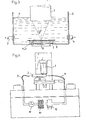
Wie in Fig. 1 a dargestellt, wird ein einfallendes Strahlenbüschel daran gehindert, in einer Vertiefung der Oberfläche beispielsweise einer Halbleiterscheibe liegende Punkte zu erreichen, wenn die zur Vertiefung führende Böschung steiler ist als der Lichteinfall, wenn also gilt α-ϑ . Wie aus Fig. 1 b hervorgeht, treten jedoch störende Effekte auch bereits dann auf, wenn die einfallenden Strahlen die zur Vertiefung führende Böschung zwar noch treffen, jedoch nahezu parallel zu dieser einfallen. Eine derartige streifende Inzidenz führt zu Unterbelichtung des Böschungsbereiches und entsprechender überbelichtung des Grundes der Vertiefung durch reflektierte Strahlen. Im Zusammenhang mit Fig. 2, welche den Querschnitt durch die Oberflächenstruktur einer bereits mehreren Belichtungsschritten unterworfenen Halbleiterscheibe, wenn auch in zehnfacher Überhöhung, zeigt, wird klar, daß die Begrenzung des öffnungswinkels zur Vermeidung von Vignettierungseffekten ein wesentliches Anliegen der Halbleiterlithographie ist.As shown in Fig. 1 a, an incident bundle of rays is prevented from reaching points lying in a depression of the surface of a semiconductor wafer, for example, if the slope leading to the depression is steeper than the incidence of light, so if α-ϑ applies. As can be seen from FIG. 1 b, however, disruptive effects also occur when the incident rays still hit the embankment leading to the depression, but are incident almost parallel to it. Such a grazing incidence leads to underexposure of the embankment area and corresponding overexposure to the bottom of the depression by reflected rays. In connection with FIG. 2, which shows the cross section through the surface structure of a semiconductor wafer which has already been subjected to several exposure steps, even if it is increased tenfold, it becomes clear that the limitation of the opening angle to avoid vignetting effects is a major concern of semiconductor lithography.
Wie ebenfalls aus.Fig. 2 hervorgeht, weist die photoempfindliche Lackschicht 7 auf der Scheibe 8 erhebliche Dickenunterschiede auf. Diese rühren daher, daß nach dem Auftragen der flüssige Lack zunächst ungeachtet der darunterliegenden Struktur eine ebene Lackoberfläche bildet, die nach dem Trocknen infolge des Entweichens des Lösungsmittels zwar in etwa, jedoch nicht genau, dem Profil der Substratoberfläche folgt. Vertiefungen der Oberfläche sind mit einer wesentlich höheren Lackschicht bedeckt, als Vorsprünge der Oberfläche.As also from Fig. 2, the
Die dargestellten Schwankungen in der Lackdicke führen dadurch zu erheblichen Konsequenzen, als es von der Lackdicke abhängt, ob sich die in der Lackschicht entstehenden stehenden Wellen durch Interferenz verstärken oder schwächen. Betreffend die dieser Erscheinung zugrunde liegende Theorie wird beispielsweise auf die ArbeitenThe fluctuations in the paint thickness shown lead This has considerable consequences as it depends on the thickness of the lacquer whether the standing waves in the lacquer layer are strengthened or weakened by interference. Regarding the theory underlying this phenomenon, for example, the work
J.D.Cuthbert, Solid State Technology, August 1977, Seite 59J.D. Cuthbert, Solid State Technology, August 1977, page 59
Dietrich W. Widmann, Apllied Optics, April 1975, Vol 14, No. 4, Seite 932Dietrich W. Widmann, Apllied Optics, April 1975, Vol 14, No. 4, page 932
Dietrich W. Widmann and Hans Binder, IEEE Transactions on Electron Devices, Vol.ED-22, No. 7, July 1975, Seite 467 - 469Dietrich W. Widmann and Hans Binder, IEEE Transactions on Electron Devices, Vol.ED-22, No. 7, July 1975, pages 467-469
verwiesen. Im ungünstigsten Fall kann durch Unterschiede in der Lackdicke trotz homogener Belichtung ein örtlicher Unterschied in der Belichtungsintensität entstehen, welcher für die wenig belichteten Bereiche eine Verlängerung der Belichtungszeit um den Faktor 2,5 bedingt. Gravierender als die dadurch generell notwendig werdende Verlängerung der Belichtungszeit ist die Tatsache, daß die durch die Dickenunterschiede der Lackschicht bedingte verschiedene Lichtempfindlichkeit der einzelnen Oberflächenbereiche höhere Anforderungen an den Bildkontrast bedingt, d.h. die Möglichkeit der Abbildung feinerer Linien herabsetzt.referred. In the worst case, differences in the thickness of the lacquer, despite homogeneous exposure, can result in a local difference in the exposure intensity, which means that the exposure time is extended by a factor of 2.5 for the less exposed areas. More serious than the generally necessary increase in the exposure time is the fact that the different light sensitivity of the individual surface areas due to the differences in thickness of the lacquer layer places higher demands on the image contrast, i.e. reduces the possibility of mapping finer lines.
Wie bereits ausgeführt worden ist, lassen sich die angeführten Nachteile vermeiden, wenn die zu belichtende Halbleiterscheibe 8 bei der Belichtung ebenso wie das Projektionsobjektiv 3 in eine Flüssigkeit 6 eingetaucht wird, wie in Fig. 3 schematisch dargestellt ist. Einige Flüssigkeiten, die im Rahmen der Erfindung verwendbar sind, werden anschließend zusammen mit ihrem Brechungsindex, der in etwa jenem von Photolack (n = 1,6) entspricht, angeführt.

Alle diese Flüssigkeiten wirken gegenüber dem Photolack benetzend. Sie liegen dicht an der Oberfläche des Lacks an, wobei Verunreinigungen unterspült und damit optisch unwirksam gemacht werden. Die zweitgenannte Gruppe von Flüssigkeiten hat zudem den Vorzugdaß sie kleinste Wassertröpfchen aufzulösen vermögen, sodaß diese nicht als kleine Kugellinsen wirken können.All of these liquids have a wetting effect on the photoresist. They lie close to the surface of the lacquer, whereby contaminants are washed down and thus rendered ineffective. The second group of liquids also has the advantage that they can dissolve the smallest water droplets, so that they cannot act as small spherical lenses.
Wie bereits ausgeführt worden ist, erhöht sich durch die Verwendung der Immersionsflüssigkeit 6 automatisch die numerische Apertur der Anordnung entsprechend dem Brechungsindex der Flüssigkeit, wodurch das Auflösungsvermögen steigt. Außerdem ergibt sich die Möglichkeit, bei der Konstruktion des Objektivs mit dem öffnungswinkel bis an die durch das Auftreten von Vignettierung gegebene Grenze zu gehen, da bei einem bestimmten öffnungswinkel der Bildfehler eines Immersionsobjektivs geringer ist als der des trockenen Systems. Gleichzeitig erlaubt der Wegfall der beim trockenen System an der Lackoberfläche entstehenden Effekte eine Abbildung bei wesentlich herabgesetztem Bildkontrast und damit eine weitere Herabsetzung der übertragbaren Linienbreite. Ein weiterer Effekt, der mit der optischen Einrichtung und dem durch diese abgebildeten Muster nichts zu tun hat, in seiner Bedeutung jedoch keineswegs unterschätzt werden soll, wird anschließend diskutiert:
- Obwohl die Vorbereitung der Halbleiterscheiben für die Belichtung unter Bedingungen erfolgt, die denen für einen chirurgischen Eingriff entsprechen, ist es fast unmöglich, die Scheiben völlig staubfrei unter die Belichtungseinrichtung zu bringen. Bei der Feinheit der erzeugten Strukturen kann sich aber bereits ein normales Staubkorn dahin auswirken, daß der erzeugte Schaltkreis unbrauchbar ist. Die Ausschußrate bei den heute angewendeten Verfahren ist daher hoch, obwohl versucht wird z.B. durch Abblasen der Halbleiterscheibe kurz vor der Belichtung restliche Staubteilchen zu entfernen. Ein weiteres Problem in der Schwierigkeit, die Temperatur im Belichtungsbereich möglichst konstant zu halten, wobei Schwankungen über 10 C bereits ausgesprochen schädlich sind.
- Although the preparation of the semiconductor wafers for the exposure takes place under conditions which correspond to those for a surgical intervention, it is almost impossible to bring the wafers under the exposure device completely dust-free. With the fineness of the structures produced, however, a normal grain of dust can have the effect that the circuit produced is unusable. The reject rate in the methods used today is therefore high, although attempts are made, for example, to remove residual dust particles by blowing off the semiconductor wafer shortly before the exposure. Another problem in the difficulty of keeping the temperature in the exposure area as constant as possible, with fluctuations above 1 0 C being extremely harmful.
Sowohl die Reinigung wie die Temperaturstabilisierung der Halbleiterscheibe ergeben sich bei der in Fig. 3 und 4 dargestellten Einrichtung als natürliche Folge des erfinderischen Grundgedankens. Die auf dem Träger 1 durch Vakuumleitungen 9 festgehaltene Halbleiterscheibe 8 wird von der Flüssigkeit 6 sowohl rein gehalten wie temperiert, wobei durch in den Behälter 2 führende Zuleitungen 4 und Ableitungen 5 stets konstante Verhältnisse hergestellt werden. Diese Zu- bzw. Ableitungen, die flexibel gestaltet sind und die zur schrittweisen Belichtung notwendige Verschiebung in den Richtungen X und Y und die Justierung in Z-Richtung erlauben, gehören zu einem Kreislauf, der außer einem nicht dargestellten Vorratsbehälter eine Pumpe 10, ein Filter 11 und eine in Abhängigkeit von der festgestellten Temperatur heizende oder kühlende Temperiereinrichtung 12 umfaßt.Both the cleaning and the temperature stabilization of the semiconductor wafer result in the device shown in FIGS. 3 and 4 as a natural consequence of the inventive concept. The
Claims (9)
Priority Applications (3)
| Application Number | Priority Date | Filing Date | Title |
|---|---|---|---|
| DE7979102675T DE2963537D1 (en) | 1979-07-27 | 1979-07-27 | Optical lithographic method and apparatus for copying a pattern onto a semiconductor wafer |
| EP79102675A EP0023231B1 (en) | 1979-07-27 | 1979-07-27 | Optical lithographic method and apparatus for copying a pattern onto a semiconductor wafer |
| AT79102675T ATE1462T1 (en) | 1979-07-27 | 1979-07-27 | OPTICAL LITHOGRAPHY PROCESS AND DEVICE FOR COPYING A PATTERN ONTO A SEMICONDUCTOR DISC. |
Applications Claiming Priority (1)
| Application Number | Priority Date | Filing Date | Title |
|---|---|---|---|
| EP79102675A EP0023231B1 (en) | 1979-07-27 | 1979-07-27 | Optical lithographic method and apparatus for copying a pattern onto a semiconductor wafer |
Publications (2)
| Publication Number | Publication Date |
|---|---|
| EP0023231A1 true EP0023231A1 (en) | 1981-02-04 |
| EP0023231B1 EP0023231B1 (en) | 1982-08-11 |
Family
ID=8186163
Family Applications (1)
| Application Number | Title | Priority Date | Filing Date |
|---|---|---|---|
| EP79102675A Expired EP0023231B1 (en) | 1979-07-27 | 1979-07-27 | Optical lithographic method and apparatus for copying a pattern onto a semiconductor wafer |
Country Status (3)
| Country | Link |
|---|---|
| EP (1) | EP0023231B1 (en) |
| AT (1) | ATE1462T1 (en) |
| DE (1) | DE2963537D1 (en) |
Cited By (162)
| Publication number | Priority date | Publication date | Assignee | Title |
|---|---|---|---|---|
| EP0060729A2 (en) * | 1981-03-18 | 1982-09-22 | Hitachi, Ltd. | Pattern forming apparatus |
| US4396705A (en) * | 1980-09-19 | 1983-08-02 | Hitachi, Ltd. | Pattern forming method and pattern forming apparatus using exposures in a liquid |
| EP0418427A2 (en) * | 1989-09-06 | 1991-03-27 | Eiichi Miyake | Exposure process |
| EP0605103A1 (en) * | 1992-11-27 | 1994-07-06 | Canon Kabushiki Kaisha | Projection apparatus for immersed exposure |
| WO2003077037A1 (en) * | 2002-03-08 | 2003-09-18 | Carl Zeiss Smt Ag | Refractive projection objective for immersion lithography |
| EP1530086A1 (en) * | 2003-11-05 | 2005-05-11 | DSM IP Assets B.V. | A method and an apparatus for producing micro-chips |
| WO2005050324A2 (en) * | 2003-11-05 | 2005-06-02 | Dsm Ip Assets B.V. | A method and apparatus for producing microchips |
| US6952253B2 (en) | 2002-11-12 | 2005-10-04 | Asml Netherlands B.V. | Lithographic apparatus and device manufacturing method |
| EP1606670A2 (en) * | 2003-03-04 | 2005-12-21 | Pixelligent Technologies LLC, | Applications of semiconductor nano-sized particles for photolithography |
| US7009682B2 (en) | 2002-11-18 | 2006-03-07 | Asml Netherlands B.V. | Lithographic apparatus and device manufacturing method |
| US7012673B2 (en) | 2003-06-27 | 2006-03-14 | Asml Netherlands B.V. | Lithographic apparatus and device manufacturing method |
| WO2006003373A3 (en) * | 2004-07-01 | 2006-03-30 | Boc Group Plc | Immersion photolithography system |
| US7034917B2 (en) | 2004-04-01 | 2006-04-25 | Asml Netherlands B.V. | Lithographic apparatus, device manufacturing method and device manufactured thereby |
| US7038760B2 (en) | 2003-06-30 | 2006-05-02 | Asml Netherlands B.V. | Lithographic apparatus and device manufacturing method |
| WO2006045748A2 (en) * | 2004-10-22 | 2006-05-04 | Carl Zeiss Smt Ag | Projection exposure apparatus for microlithography |
| US7050146B2 (en) | 2004-02-09 | 2006-05-23 | Asml Netherlands B.V. | Lithographic apparatus and device manufacturing method |
| US7075616B2 (en) | 2002-11-12 | 2006-07-11 | Asml Netherlands B.V. | Lithographic apparatus and device manufacturing method |
| US7081943B2 (en) | 2002-11-12 | 2006-07-25 | Asml Netherlands B.V. | Lithographic apparatus and device manufacturing method |
| US7085075B2 (en) | 2003-08-12 | 2006-08-01 | Carl Zeiss Smt Ag | Projection objectives including a plurality of mirrors with lenses ahead of mirror M3 |
| US7092069B2 (en) | 2002-03-08 | 2006-08-15 | Carl Zeiss Smt Ag | Projection exposure method and projection exposure system |
| US7110087B2 (en) | 2003-06-30 | 2006-09-19 | Asml Netherlands B.V. | Lithographic apparatus and device manufacturing method |
| US7110081B2 (en) | 2002-11-12 | 2006-09-19 | Asml Netherlands B.V. | Lithographic apparatus and device manufacturing method |
| US7119876B2 (en) | 2004-10-18 | 2006-10-10 | Asml Netherlands B.V. | Lithographic apparatus and device manufacturing method |
| US7119874B2 (en) | 2003-06-27 | 2006-10-10 | Asml Netherlands B.V. | Lithographic apparatus and device manufacturing method |
| US7133114B2 (en) | 2004-09-20 | 2006-11-07 | Asml Netherlands B.V. | Lithographic apparatus and device manufacturing method |
| US7145630B2 (en) | 2004-11-23 | 2006-12-05 | Asml Netherlands B.V. | Lithographic apparatus and device manufacturing method |
| US7158211B2 (en) | 2003-09-29 | 2007-01-02 | Asml Netherlands B.V. | Lithographic apparatus and device manufacturing method |
| US7161654B2 (en) | 2004-12-02 | 2007-01-09 | Asml Netherlands B.V. | Lithographic apparatus and device manufacturing method |
| US7161663B2 (en) | 2004-07-22 | 2007-01-09 | Asml Netherlands B.V. | Lithographic apparatus |
| US7175968B2 (en) | 2003-07-28 | 2007-02-13 | Asml Netherlands B.V. | Lithographic apparatus, device manufacturing method and a substrate |
| US7184122B2 (en) | 2003-07-24 | 2007-02-27 | Asml Netherlands B.V. | Lithographic apparatus and device manufacturing method |
| EP1759248A1 (en) * | 2004-06-04 | 2007-03-07 | Carl Zeiss SMT AG | Projection system with compensation of intensity variatons and compensation element therefor |
| US7193232B2 (en) | 2002-11-12 | 2007-03-20 | Asml Netherlands B.V. | Lithographic apparatus and device manufacturing method with substrate measurement not through liquid |
| US7193681B2 (en) | 2003-09-29 | 2007-03-20 | Asml Netherlands B.V. | Lithographic apparatus and device manufacturing method |
| US7196770B2 (en) | 2004-12-07 | 2007-03-27 | Asml Netherlands B.V. | Prewetting of substrate before immersion exposure |
| US7199858B2 (en) | 2002-11-12 | 2007-04-03 | Asml Netherlands B.V. | Lithographic apparatus and device manufacturing method |
| US7209213B2 (en) | 2004-10-07 | 2007-04-24 | Asml Netherlands B.V. | Lithographic apparatus and device manufacturing method |
| US7213963B2 (en) | 2003-06-09 | 2007-05-08 | Asml Netherlands B.V. | Lithographic apparatus and device manufacturing method |
| US7224431B2 (en) | 2005-02-22 | 2007-05-29 | Asml Netherlands B.V. | Lithographic apparatus and device manufacturing method |
| US7227619B2 (en) | 2004-04-01 | 2007-06-05 | Asml Netherlands B.V. | Lithographic apparatus and device manufacturing method |
| US7227616B2 (en) | 2002-12-10 | 2007-06-05 | Carl Zeiss Smt Ag | Method for improving an optical imaging property of a projection objective of a microlithographic projection exposure apparatus |
| US7242455B2 (en) | 2002-12-10 | 2007-07-10 | Nikon Corporation | Exposure apparatus and method for producing device |
| US7244665B2 (en) | 2004-04-29 | 2007-07-17 | Micron Technology, Inc. | Wafer edge ring structures and methods of formation |
| US7248334B2 (en) | 2004-12-07 | 2007-07-24 | Asml Netherlands B.V. | Sensor shield |
| US7251013B2 (en) | 2004-11-12 | 2007-07-31 | Asml Netherlands B.V. | Lithographic apparatus and device manufacturing method |
| US7253879B2 (en) | 2005-04-19 | 2007-08-07 | Asml Holding N.V. | Liquid immersion lithography system with tilted liquid flow |
| US7291850B2 (en) | 2005-04-08 | 2007-11-06 | Asml Netherlands B.V. | Lithographic apparatus and device manufacturing method |
| US7295283B2 (en) | 2004-04-02 | 2007-11-13 | Asml Netherlands B.V. | Lithographic apparatus and device manufacturing method |
| US7304715B2 (en) | 2004-08-13 | 2007-12-04 | Asml Netherlands B.V. | Lithographic apparatus and device manufacturing method |
| US7317507B2 (en) | 2005-05-03 | 2008-01-08 | Asml Netherlands B.V. | Lithographic apparatus and device manufacturing method |
| US7317504B2 (en) | 2004-04-08 | 2008-01-08 | Asml Netherlands B.V. | Lithographic apparatus and device manufacturing method |
| US7324185B2 (en) | 2005-03-04 | 2008-01-29 | Asml Netherlands B.V. | Lithographic apparatus and device manufacturing method |
| US7326522B2 (en) | 2004-02-11 | 2008-02-05 | Asml Netherlands B.V. | Device manufacturing method and a substrate |
| US7330238B2 (en) | 2005-03-28 | 2008-02-12 | Asml Netherlands, B.V. | Lithographic apparatus, immersion projection apparatus and device manufacturing method |
| US7352433B2 (en) | 2003-10-28 | 2008-04-01 | Asml Netherlands B.V. | Lithographic apparatus and device manufacturing method |
| US7352440B2 (en) | 2004-12-10 | 2008-04-01 | Asml Netherlands B.V. | Substrate placement in immersion lithography |
| US7352434B2 (en) | 2003-05-13 | 2008-04-01 | Asml Netherlands B.V. | Lithographic apparatus and device manufacturing method |
| US7352435B2 (en) | 2003-10-15 | 2008-04-01 | Asml Netherlands B.V. | Lithographic apparatus and device manufacturing method |
| US7355674B2 (en) | 2004-09-28 | 2008-04-08 | Asml Netherlands B.V. | Lithographic apparatus, device manufacturing method and computer program product |
| US7359030B2 (en) | 2002-11-29 | 2008-04-15 | Asml Netherlands B.V. | Lithographic apparatus and device manufacturing method |
| US7365827B2 (en) | 2004-12-08 | 2008-04-29 | Asml Netherlands B.V. | Lithographic apparatus and device manufacturing method |
| US7379155B2 (en) | 2004-10-18 | 2008-05-27 | Asml Netherlands B.V. | Lithographic apparatus and device manufacturing method |
| US7379159B2 (en) | 2004-05-03 | 2008-05-27 | Asml Netherlands B.V. | Lithographic apparatus and device manufacturing method |
| US7378025B2 (en) | 2005-02-22 | 2008-05-27 | Asml Netherlands B.V. | Fluid filtration method, fluid filtered thereby, lithographic apparatus and device manufacturing method |
| US7385764B2 (en) | 2003-12-15 | 2008-06-10 | Carl Zeiss Smt Ag | Objectives as a microlithography projection objective with at least one liquid lens |
| US7394521B2 (en) | 2003-12-23 | 2008-07-01 | Asml Netherlands B.V. | Lithographic apparatus and device manufacturing method |
| WO2008080521A2 (en) * | 2006-12-28 | 2008-07-10 | Dsm Ip Assets B.V. | Immersion fluid and method for producing microchips |
| US7403261B2 (en) | 2004-12-15 | 2008-07-22 | Asml Netherlands B.V. | Lithographic apparatus and device manufacturing method |
| US7405805B2 (en) | 2004-12-28 | 2008-07-29 | Asml Netherlands B.V. | Lithographic apparatus and device manufacturing method |
| US7411657B2 (en) | 2004-11-17 | 2008-08-12 | Asml Netherlands B.V. | Lithographic apparatus and device manufacturing method |
| US7411658B2 (en) | 2005-10-06 | 2008-08-12 | Asml Netherlands B.V. | Lithographic apparatus and device manufacturing method |
| US7411654B2 (en) | 2005-04-05 | 2008-08-12 | Asml Netherlands B.V. | Lithographic apparatus and device manufacturing method |
| US7411650B2 (en) | 2003-06-19 | 2008-08-12 | Asml Holding N.V. | Immersion photolithography system and method using microchannel nozzles |
| US7414699B2 (en) | 2004-11-12 | 2008-08-19 | Asml Netherlands B.V. | Lithographic apparatus and device manufacturing method |
| US7420194B2 (en) | 2005-12-27 | 2008-09-02 | Asml Netherlands B.V. | Lithographic apparatus and substrate edge seal |
| US7423720B2 (en) | 2004-11-12 | 2008-09-09 | Asml Netherlands B.V. | Lithographic apparatus and device manufacturing method |
| US7428038B2 (en) | 2005-02-28 | 2008-09-23 | Asml Netherlands B.V. | Lithographic apparatus, device manufacturing method and apparatus for de-gassing a liquid |
| US7433016B2 (en) | 2005-05-03 | 2008-10-07 | Asml Netherlands B.V. | Lithographic apparatus and device manufacturing method |
| US7433015B2 (en) | 2003-10-15 | 2008-10-07 | Asml Netherlands B.V. | Lithographic apparatus and device manufacturing method |
| US7446850B2 (en) | 2004-12-03 | 2008-11-04 | Asml Netherlands B.V. | Lithographic apparatus and device manufacturing method |
| US7468779B2 (en) | 2005-06-28 | 2008-12-23 | Asml Netherlands B.V. | Lithographic apparatus and device manufacturing method |
| US7474379B2 (en) | 2005-06-28 | 2009-01-06 | Asml Netherlands B.V. | Lithographic apparatus and device manufacturing method |
| US7486381B2 (en) | 2004-05-21 | 2009-02-03 | Asml Netherlands B.V. | Lithographic apparatus and device manufacturing method |
| US7491661B2 (en) | 2004-12-28 | 2009-02-17 | Asml Netherlands B.V. | Device manufacturing method, top coat material and substrate |
| US7522261B2 (en) | 2004-09-24 | 2009-04-21 | Asml Netherlands B.V. | Lithographic apparatus and device manufacturing method |
| US7528931B2 (en) | 2004-12-20 | 2009-05-05 | Asml Netherlands B.V. | Lithographic apparatus and device manufacturing method |
| US7532306B2 (en) | 2003-05-30 | 2009-05-12 | Carl Zeiss Smt Ag | Microlithographic projection exposure apparatus |
| US7535644B2 (en) | 2005-08-12 | 2009-05-19 | Asml Netherlands B.V. | Lens element, lithographic apparatus, device manufacturing method, and device manufactured thereby |
| US7545481B2 (en) | 2003-11-24 | 2009-06-09 | Asml Netherlands B.V. | Lithographic apparatus and device manufacturing method |
| US7583357B2 (en) | 2004-11-12 | 2009-09-01 | Asml Netherlands B.V. | Lithographic apparatus and device manufacturing method |
| US7589818B2 (en) | 2003-12-23 | 2009-09-15 | Asml Netherlands B.V. | Lithographic apparatus, alignment apparatus, device manufacturing method, and a method of converting an apparatus |
| US7633073B2 (en) | 2005-11-23 | 2009-12-15 | Asml Netherlands B.V. | Lithographic apparatus and device manufacturing method |
| US7649611B2 (en) | 2005-12-30 | 2010-01-19 | Asml Netherlands B.V. | Lithographic apparatus and device manufacturing method |
| US7652746B2 (en) | 2005-06-21 | 2010-01-26 | Asml Netherlands B.V. | Lithographic apparatus and device manufacturing method |
| US7656501B2 (en) | 2005-11-16 | 2010-02-02 | Asml Netherlands B.V. | Lithographic apparatus |
| US7670730B2 (en) | 2004-12-30 | 2010-03-02 | Asml Netherlands B.V. | Lithographic apparatus and device manufacturing method |
| EP2161620A1 (en) * | 2003-04-11 | 2010-03-10 | Nikon Corporation | Cleanup method for optics in immersion lithography |
| US7684010B2 (en) | 2005-03-09 | 2010-03-23 | Asml Netherlands B.V. | Lithographic apparatus, device manufacturing method, seal structure, method of removing an object and a method of sealing |
| US7705962B2 (en) | 2005-01-14 | 2010-04-27 | Asml Netherlands B.V. | Lithographic apparatus and device manufacturing method |
| US7719658B2 (en) | 2004-02-13 | 2010-05-18 | Carl Zeiss Smt Ag | Imaging system for a microlithographical projection light system |
| US7733459B2 (en) | 2003-08-29 | 2010-06-08 | Asml Netherlands B.V. | Lithographic apparatus and device manufacturing method |
| US7738074B2 (en) | 2003-07-16 | 2010-06-15 | Asml Netherlands B.V. | Lithographic apparatus and device manufacturing method |
| US7751027B2 (en) | 2005-06-21 | 2010-07-06 | Asml Netherlands B.V. | Lithographic apparatus and device manufacturing method |
| US7773195B2 (en) | 2005-11-29 | 2010-08-10 | Asml Holding N.V. | System and method to increase surface tension and contact angle in immersion lithography |
| US7791709B2 (en) | 2006-12-08 | 2010-09-07 | Asml Netherlands B.V. | Substrate support and lithographic process |
| US7804577B2 (en) | 2005-11-16 | 2010-09-28 | Asml Netherlands B.V. | Lithographic apparatus |
| US7804574B2 (en) | 2003-05-30 | 2010-09-28 | Asml Netherlands B.V. | Lithographic apparatus and device manufacturing method using acidic liquid |
| US7817245B2 (en) | 2003-09-29 | 2010-10-19 | Asml Netherlands B.V. | Lithographic apparatus and device manufacturing method |
| US7834974B2 (en) | 2005-06-28 | 2010-11-16 | Asml Netherlands B.V. | Lithographic apparatus and device manufacturing method |
| US7839483B2 (en) | 2005-12-28 | 2010-11-23 | Asml Netherlands B.V. | Lithographic apparatus, device manufacturing method and a control system |
| US7855777B2 (en) | 2003-07-09 | 2010-12-21 | Nikon Corporation | Exposure apparatus and method for manufacturing device |
| US7864292B2 (en) | 2005-11-16 | 2011-01-04 | Asml Netherlands B.V. | Lithographic apparatus and device manufacturing method |
| US7894040B2 (en) | 2004-10-05 | 2011-02-22 | Asml Netherlands B.V. | Lithographic apparatus and device manufacturing method |
| US7898642B2 (en) | 2004-04-14 | 2011-03-01 | Asml Netherlands B.V. | Lithographic apparatus and device manufacturing method |
| US7898643B2 (en) | 2003-06-27 | 2011-03-01 | Asml Holding N.V. | Immersion photolithography system and method using inverted wafer-projection optics interface |
| US8007986B2 (en) | 2004-01-23 | 2011-08-30 | Air Products And Chemicals, Inc. | Immersion lithography fluids |
| US8018573B2 (en) | 2005-02-22 | 2011-09-13 | Asml Netherlands B.V. | Lithographic apparatus and device manufacturing method |
| US8045134B2 (en) | 2006-03-13 | 2011-10-25 | Asml Netherlands B.V. | Lithographic apparatus, control system and device manufacturing method |
| US8045135B2 (en) | 2006-11-22 | 2011-10-25 | Asml Netherlands B.V. | Lithographic apparatus with a fluid combining unit and related device manufacturing method |
| US8054445B2 (en) | 2005-08-16 | 2011-11-08 | Asml Netherlands B.V. | Lithographic apparatus and device manufacturing method |
| US8072576B2 (en) | 2003-05-23 | 2011-12-06 | Nikon Corporation | Exposure apparatus and method for producing device |
| US8164734B2 (en) | 2004-06-16 | 2012-04-24 | Asml Netherlands B.V. | Vacuum system for immersion photolithography |
| US8208123B2 (en) | 2003-08-29 | 2012-06-26 | Asml Netherlands B.V. | Lithographic apparatus and device manufacturing method |
| US8208124B2 (en) | 2003-08-29 | 2012-06-26 | Asml Netherlands B.V. | Lithographic apparatus and device manufacturing method |
| US8248577B2 (en) | 2005-05-03 | 2012-08-21 | Asml Netherlands B.V. | Lithographic apparatus and device manufacturing method |
| US8379187B2 (en) | 2007-10-24 | 2013-02-19 | Nikon Corporation | Optical unit, illumination optical apparatus, exposure apparatus, and device manufacturing method |
| US8446579B2 (en) | 2008-05-28 | 2013-05-21 | Nikon Corporation | Inspection device and inspecting method for spatial light modulator, illumination optical system, method for adjusting the illumination optical system, exposure apparatus, and device manufacturing method |
| US8451427B2 (en) | 2007-09-14 | 2013-05-28 | Nikon Corporation | Illumination optical system, exposure apparatus, optical element and manufacturing method thereof, and device manufacturing method |
| US8462317B2 (en) | 2007-10-16 | 2013-06-11 | Nikon Corporation | Illumination optical system, exposure apparatus, and device manufacturing method |
| US8520184B2 (en) | 2004-06-09 | 2013-08-27 | Nikon Corporation | Immersion exposure apparatus and device manufacturing method with measuring device |
| US8520291B2 (en) | 2007-10-16 | 2013-08-27 | Nikon Corporation | Illumination optical system, exposure apparatus, and device manufacturing method |
| US20130271945A1 (en) | 2004-02-06 | 2013-10-17 | Nikon Corporation | Polarization-modulating element, illumination optical apparatus, exposure apparatus, and exposure method |
| US8634053B2 (en) | 2006-12-07 | 2014-01-21 | Asml Netherlands B.V. | Lithographic apparatus and device manufacturing method |
| US8675177B2 (en) | 2003-04-09 | 2014-03-18 | Nikon Corporation | Exposure method and apparatus, and method for fabricating device with light amount distribution having light larger in first and second pairs of areas |
| US8705009B2 (en) | 2009-09-28 | 2014-04-22 | Asml Netherlands B.V. | Heat pipe, lithographic apparatus and device manufacturing method |
| US8854601B2 (en) | 2005-05-12 | 2014-10-07 | Nikon Corporation | Projection optical system, exposure apparatus, and exposure method |
| US8859188B2 (en) | 2005-02-10 | 2014-10-14 | Asml Netherlands B.V. | Immersion liquid, exposure apparatus, and exposure process |
| US8879159B2 (en) | 2005-06-14 | 2014-11-04 | Carl Zeiss Smt Gmbh | Lithography projection objective, and a method for correcting image defects of the same |
| US8993221B2 (en) | 2012-02-10 | 2015-03-31 | Pixelligent Technologies, Llc | Block co-polymer photoresist |
| US9081295B2 (en) | 2003-05-06 | 2015-07-14 | Nikon Corporation | Catadioptric projection optical system, exposure apparatus, and exposure method |
| US9097981B2 (en) | 2007-10-12 | 2015-08-04 | Nikon Corporation | Illumination optical apparatus, exposure apparatus, and device manufacturing method |
| US9116346B2 (en) | 2007-11-06 | 2015-08-25 | Nikon Corporation | Illumination apparatus, illumination method, exposure apparatus, and device manufacturing method |
| US9140992B2 (en) | 2003-10-28 | 2015-09-22 | Nikon Corporation | Illumination optical apparatus and projection exposure apparatus |
| US9164209B2 (en) | 2003-11-20 | 2015-10-20 | Nikon Corporation | Illumination optical apparatus, exposure apparatus, and exposure method with optical member with optical rotatory power having different thicknesses to rotate linear polarization direction |
| US9477158B2 (en) | 2006-04-14 | 2016-10-25 | Asml Netherlands B.V. | Lithographic apparatus and device manufacturing method |
| US9500943B2 (en) | 2003-05-06 | 2016-11-22 | Nikon Corporation | Projection optical system, exposure apparatus, and exposure method |
| US9623436B2 (en) | 2004-05-18 | 2017-04-18 | Asml Netherlands B.V. | Active drying station and method to remove immersion liquid using gas flow supply with gas outlet between two gas inlets |
| US9632425B2 (en) | 2006-12-07 | 2017-04-25 | Asml Holding N.V. | Lithographic apparatus, a dryer and a method of removing liquid from a surface |
| US9639006B2 (en) | 2003-07-28 | 2017-05-02 | Asml Netherlands B.V. | Lithographic projection apparatus and device manufacturing method |
| US9703210B2 (en) | 2004-12-20 | 2017-07-11 | Asml Netherlands B.V. | Lithographic apparatus and device manufacturing method |
| US9746788B2 (en) | 2004-08-19 | 2017-08-29 | Asml Netherlands B.V. | Lithographic apparatus and device manufacturing method |
| US9746781B2 (en) | 2005-01-31 | 2017-08-29 | Nikon Corporation | Exposure apparatus and method for producing device |
| US9766555B2 (en) | 2003-02-26 | 2017-09-19 | Nikon Corporation | Exposure apparatus, exposure method, and method for producing device |
| EP3223074A1 (en) * | 2003-09-03 | 2017-09-27 | Nikon Corporation | Apparatus and method for immersion lithography for recovering fluid |
| US9846372B2 (en) | 2010-04-22 | 2017-12-19 | Asml Netherlands B.V. | Fluid handling structure, lithographic apparatus and device manufacturing method |
| US9952515B2 (en) | 2003-11-14 | 2018-04-24 | Asml Netherlands B.V. | Lithographic apparatus and device manufacturing method |
| US9964858B2 (en) | 2003-06-11 | 2018-05-08 | Asml Netherlands B.V. | Lithographic apparatus and device manufacturing method |
| US10025204B2 (en) | 2003-08-29 | 2018-07-17 | Asml Netherlands B.V. | Lithographic apparatus and device manufacturing method |
| US10248034B2 (en) | 2003-10-28 | 2019-04-02 | Asml Netherlands B.V. | Lithographic apparatus and device manufacturing method |
| US10261428B2 (en) | 2002-11-12 | 2019-04-16 | Asml Netherlands B.V. | Lithographic apparatus and device manufacturing method |
| US10338478B2 (en) | 2004-07-07 | 2019-07-02 | Asml Netherlands B.V. | Lithographic apparatus and device manufacturing method |
| US10503084B2 (en) | 2002-11-12 | 2019-12-10 | Asml Netherlands B.V. | Lithographic apparatus and device manufacturing method |
Families Citing this family (16)
| Publication number | Priority date | Publication date | Assignee | Title |
|---|---|---|---|---|
| JP2005536775A (en) | 2002-08-23 | 2005-12-02 | 株式会社ニコン | Projection optical system, photolithography method and exposure apparatus, and method using exposure apparatus |
| US7779781B2 (en) | 2003-07-31 | 2010-08-24 | Asml Netherlands B.V. | Lithographic apparatus and device manufacturing method |
| US8149381B2 (en) | 2003-08-26 | 2012-04-03 | Nikon Corporation | Optical element and exposure apparatus |
| SG133590A1 (en) | 2003-08-26 | 2007-07-30 | Nikon Corp | Optical element and exposure device |
| US7713841B2 (en) | 2003-09-19 | 2010-05-11 | Micron Technology, Inc. | Methods for thinning semiconductor substrates that employ support structures formed on the substrates |
| US7113259B2 (en) | 2003-10-31 | 2006-09-26 | Asml Netherlands B.V. | Lithographic apparatus and device manufacturing method |
| US7397533B2 (en) | 2004-12-07 | 2008-07-08 | Asml Netherlands B.V. | Lithographic apparatus and device manufacturing method |
| SG124351A1 (en) | 2005-01-14 | 2006-08-30 | Asml Netherlands Bv | Lithographic apparatus and device manufacturing method |
| US8692973B2 (en) | 2005-01-31 | 2014-04-08 | Nikon Corporation | Exposure apparatus and method for producing device |
| US7969548B2 (en) | 2006-05-22 | 2011-06-28 | Asml Netherlands B.V. | Lithographic apparatus and lithographic apparatus cleaning method |
| US8817226B2 (en) | 2007-02-15 | 2014-08-26 | Asml Holding N.V. | Systems and methods for insitu lens cleaning using ozone in immersion lithography |
| US8654305B2 (en) | 2007-02-15 | 2014-02-18 | Asml Holding N.V. | Systems and methods for insitu lens cleaning in immersion lithography |
| US8947629B2 (en) | 2007-05-04 | 2015-02-03 | Asml Netherlands B.V. | Cleaning device, a lithographic apparatus and a lithographic apparatus cleaning method |
| US9013672B2 (en) | 2007-05-04 | 2015-04-21 | Asml Netherlands B.V. | Cleaning device, a lithographic apparatus and a lithographic apparatus cleaning method |
| US7866330B2 (en) | 2007-05-04 | 2011-01-11 | Asml Netherlands B.V. | Cleaning device, a lithographic apparatus and a lithographic apparatus cleaning method |
| US8011377B2 (en) | 2007-05-04 | 2011-09-06 | Asml Netherlands B.V. | Cleaning device and a lithographic apparatus cleaning method |
Citations (2)
| Publication number | Priority date | Publication date | Assignee | Title |
|---|---|---|---|---|
| US3346475A (en) * | 1963-02-25 | 1967-10-10 | Australia Res Lab | Electrophotographic method using an unsymmetrical ac current during development |
| DE1944448B2 (en) * | 1969-09-02 | 1972-03-30 | Fa. Carl Zeiss, 7920 Heidenheim | METHOD AND DEVICE FOR THE PRODUCTION OF INTEGRATED SEMI-CIRCUIT CIRCUITS IN A MONOLITHIC DESIGN |
-
1979
- 1979-07-27 AT AT79102675T patent/ATE1462T1/en not_active IP Right Cessation
- 1979-07-27 EP EP79102675A patent/EP0023231B1/en not_active Expired
- 1979-07-27 DE DE7979102675T patent/DE2963537D1/en not_active Expired
Patent Citations (2)
| Publication number | Priority date | Publication date | Assignee | Title |
|---|---|---|---|---|
| US3346475A (en) * | 1963-02-25 | 1967-10-10 | Australia Res Lab | Electrophotographic method using an unsymmetrical ac current during development |
| DE1944448B2 (en) * | 1969-09-02 | 1972-03-30 | Fa. Carl Zeiss, 7920 Heidenheim | METHOD AND DEVICE FOR THE PRODUCTION OF INTEGRATED SEMI-CIRCUIT CIRCUITS IN A MONOLITHIC DESIGN |
Non-Patent Citations (3)
| Title |
|---|
| "Lexikon Technik und exakte Naturwissenschaften" Band 5: "Gesteine-Kalisalpeter " Oktober 1972, FISHER TASCHENBUCHVERLAG, Frankfurt am Main, Seite 1510 * |
| ELEKTRONIKER, 18. Jahrgang, Heft 2/Februar 1979 Fachschriftenverlag Aarau Dr. H. SCHAUMBURG "Lithographietechniken fur hochstintegrierte Schaltungen" Seiten 41 bis 43 * |
| WILHELM H. WESTPHAL "PHYSIK" 22. bis 24. Auflage 1963, SPRINGER-VERLAG, Berlin-GOTTINGEN-Heidelberg, Seite 527 bis 529 * |
Cited By (470)
| Publication number | Priority date | Publication date | Assignee | Title |
|---|---|---|---|---|
| US4396705A (en) * | 1980-09-19 | 1983-08-02 | Hitachi, Ltd. | Pattern forming method and pattern forming apparatus using exposures in a liquid |
| EP0060729A2 (en) * | 1981-03-18 | 1982-09-22 | Hitachi, Ltd. | Pattern forming apparatus |
| EP0060729A3 (en) * | 1981-03-18 | 1983-03-16 | Hitachi, Ltd. | Pattern forming apparatus |
| US4480910A (en) * | 1981-03-18 | 1984-11-06 | Hitachi, Ltd. | Pattern forming apparatus |
| EP0418427A2 (en) * | 1989-09-06 | 1991-03-27 | Eiichi Miyake | Exposure process |
| EP0418427A3 (en) * | 1989-09-06 | 1992-01-22 | Eiichi Miyake | Exposure process |
| EP0605103A1 (en) * | 1992-11-27 | 1994-07-06 | Canon Kabushiki Kaisha | Projection apparatus for immersed exposure |
| US5610683A (en) * | 1992-11-27 | 1997-03-11 | Canon Kabushiki Kaisha | Immersion type projection exposure apparatus |
| WO2003077037A1 (en) * | 2002-03-08 | 2003-09-18 | Carl Zeiss Smt Ag | Refractive projection objective for immersion lithography |
| US6891596B2 (en) | 2002-03-08 | 2005-05-10 | Carl Zeiss Smt Ag | Refractive projection objective for immersion lithography |
| US7495840B2 (en) | 2002-03-08 | 2009-02-24 | Karl-Heinz Schuster | Very high-aperture projection objective |
| US7312847B2 (en) | 2002-03-08 | 2007-12-25 | Carl Zeiss Smt Ag | Refractive projection objective for immersion lithography |
| US7203008B2 (en) | 2002-03-08 | 2007-04-10 | Carl Zeiss Smt Ag | Very high-aperture projection objective |
| US7092069B2 (en) | 2002-03-08 | 2006-08-15 | Carl Zeiss Smt Ag | Projection exposure method and projection exposure system |
| US7199858B2 (en) | 2002-11-12 | 2007-04-03 | Asml Netherlands B.V. | Lithographic apparatus and device manufacturing method |
| US7110081B2 (en) | 2002-11-12 | 2006-09-19 | Asml Netherlands B.V. | Lithographic apparatus and device manufacturing method |
| US7482611B2 (en) | 2002-11-12 | 2009-01-27 | Asml Netherlands B.V. | Lithographic apparatus and device manufacturing method |
| US9588442B2 (en) | 2002-11-12 | 2017-03-07 | Asml Netherlands B.V. | Lithographic apparatus and device manufacturing method |
| US10962891B2 (en) | 2002-11-12 | 2021-03-30 | Asml Netherlands B.V. | Lithographic apparatus and device manufacturing method |
| US9885965B2 (en) | 2002-11-12 | 2018-02-06 | Asml Netherlands B.V. | Lithographic apparatus and device manufacturing method |
| US10788755B2 (en) | 2002-11-12 | 2020-09-29 | Asml Netherlands B.V. | Lithographic apparatus and device manufacturing method |
| US9360765B2 (en) | 2002-11-12 | 2016-06-07 | Asml Netherlands B.V. | Lithographic apparatus and device manufacturing method |
| US7075616B2 (en) | 2002-11-12 | 2006-07-11 | Asml Netherlands B.V. | Lithographic apparatus and device manufacturing method |
| US7081943B2 (en) | 2002-11-12 | 2006-07-25 | Asml Netherlands B.V. | Lithographic apparatus and device manufacturing method |
| US8344341B2 (en) | 2002-11-12 | 2013-01-01 | Asml Netherlands B.V. | Lithographic apparatus and device manufacturing method |
| US7193232B2 (en) | 2002-11-12 | 2007-03-20 | Asml Netherlands B.V. | Lithographic apparatus and device manufacturing method with substrate measurement not through liquid |
| US9195153B2 (en) | 2002-11-12 | 2015-11-24 | Asml Netherlands B.V. | Lithographic apparatus and device manufacturing method |
| US9740107B2 (en) | 2002-11-12 | 2017-08-22 | Asml Netherlands B.V. | Lithographic apparatus and device manufacturing method |
| US7224436B2 (en) | 2002-11-12 | 2007-05-29 | Asml Netherlands B.V. | Lithographic apparatus and device manufacturing method |
| US7795603B2 (en) | 2002-11-12 | 2010-09-14 | Asml Netherlands B.V. | Lithographic apparatus and device manufacturing method |
| US9097987B2 (en) | 2002-11-12 | 2015-08-04 | Asml Netherlands B.V. | Lithographic apparatus and device manufacturing method |
| US8446568B2 (en) | 2002-11-12 | 2013-05-21 | Asml Netherlands B.V. | Lithographic apparatus and device manufacturing method |
| US10620545B2 (en) | 2002-11-12 | 2020-04-14 | Asml Netherlands B.V. | Lithographic apparatus and device manufacturing method |
| US10191389B2 (en) | 2002-11-12 | 2019-01-29 | Asml Netherlands B.V. | Lithographic apparatus and device manufacturing method |
| US6952253B2 (en) | 2002-11-12 | 2005-10-04 | Asml Netherlands B.V. | Lithographic apparatus and device manufacturing method |
| US10222706B2 (en) | 2002-11-12 | 2019-03-05 | Asml Netherlands B.V. | Lithographic apparatus and device manufacturing method |
| US10261428B2 (en) | 2002-11-12 | 2019-04-16 | Asml Netherlands B.V. | Lithographic apparatus and device manufacturing method |
| US10503084B2 (en) | 2002-11-12 | 2019-12-10 | Asml Netherlands B.V. | Lithographic apparatus and device manufacturing method |
| US7932999B2 (en) | 2002-11-12 | 2011-04-26 | Asml Netherlands B.V. | Lithographic apparatus and device manufacturing method |
| US7009682B2 (en) | 2002-11-18 | 2006-03-07 | Asml Netherlands B.V. | Lithographic apparatus and device manufacturing method |
| US7119881B2 (en) | 2002-11-18 | 2006-10-10 | Asml Netherlands B.V. | Lithographic apparatus and device manufacturing method |
| US7359030B2 (en) | 2002-11-29 | 2008-04-15 | Asml Netherlands B.V. | Lithographic apparatus and device manufacturing method |
| US7242455B2 (en) | 2002-12-10 | 2007-07-10 | Nikon Corporation | Exposure apparatus and method for producing device |
| US7817244B2 (en) | 2002-12-10 | 2010-10-19 | Nikon Corporation | Exposure apparatus and method for producing device |
| US7227616B2 (en) | 2002-12-10 | 2007-06-05 | Carl Zeiss Smt Ag | Method for improving an optical imaging property of a projection objective of a microlithographic projection exposure apparatus |
| US8237915B2 (en) | 2002-12-10 | 2012-08-07 | Carl Zeiss Smt Gmbh | Method for improving an optical imaging property of a projection objective of a microlithographic projection exposure apparatus |
| US7834976B2 (en) | 2002-12-10 | 2010-11-16 | Nikon Corporation | Exposure apparatus and method for producing device |
| US9766555B2 (en) | 2003-02-26 | 2017-09-19 | Nikon Corporation | Exposure apparatus, exposure method, and method for producing device |
| US10180632B2 (en) | 2003-02-26 | 2019-01-15 | Nikon Corporation | Exposure apparatus, exposure method, and method for producing device |
| EP1606670A4 (en) * | 2003-03-04 | 2009-08-05 | Pixelligent Technologies Llc | Applications of semiconductor nano-sized particles for photolithography |
| EP1606670A2 (en) * | 2003-03-04 | 2005-12-21 | Pixelligent Technologies LLC, | Applications of semiconductor nano-sized particles for photolithography |
| US9207538B2 (en) | 2003-03-04 | 2015-12-08 | Pixelligent Technologies, Llc | Applications of semiconductor nano-sized particles for photolithography |
| US9885959B2 (en) | 2003-04-09 | 2018-02-06 | Nikon Corporation | Illumination optical apparatus having deflecting member, lens, polarization member to set polarization in circumference direction, and optical integrator |
| US9678437B2 (en) | 2003-04-09 | 2017-06-13 | Nikon Corporation | Illumination optical apparatus having distribution changing member to change light amount and polarization member to set polarization in circumference direction |
| US8675177B2 (en) | 2003-04-09 | 2014-03-18 | Nikon Corporation | Exposure method and apparatus, and method for fabricating device with light amount distribution having light larger in first and second pairs of areas |
| US9164393B2 (en) | 2003-04-09 | 2015-10-20 | Nikon Corporation | Exposure method and apparatus, and method for fabricating device with light amount distribution having light larger in four areas |
| US9146474B2 (en) | 2003-04-09 | 2015-09-29 | Nikon Corporation | Exposure method and apparatus, and method for fabricating device with light amount distribution having light larger and different linear polarization states in an on-axis area and a plurality of off-axis areas |
| US8670103B2 (en) | 2003-04-11 | 2014-03-11 | Nikon Corporation | Cleanup method for optics in immersion lithography using bubbles |
| US8670104B2 (en) | 2003-04-11 | 2014-03-11 | Nikon Corporation | Cleanup method for optics in immersion lithography with cleaning liquid opposed by a surface of object |
| US8085381B2 (en) | 2003-04-11 | 2011-12-27 | Nikon Corporation | Cleanup method for optics in immersion lithography using sonic device |
| US9958786B2 (en) | 2003-04-11 | 2018-05-01 | Nikon Corporation | Cleanup method for optics in immersion lithography using object on wafer holder in place of wafer |
| EP2161620A1 (en) * | 2003-04-11 | 2010-03-10 | Nikon Corporation | Cleanup method for optics in immersion lithography |
| US8493545B2 (en) | 2003-04-11 | 2013-07-23 | Nikon Corporation | Cleanup method for optics in immersion lithography supplying cleaning liquid onto a surface of object below optical element, liquid supply port and liquid recovery port |
| US8269946B2 (en) | 2003-04-11 | 2012-09-18 | Nikon Corporation | Cleanup method for optics in immersion lithography supplying cleaning liquid at different times than immersion liquid |
| US10156792B2 (en) | 2003-05-06 | 2018-12-18 | Nikon Corporation | Projection optical system, exposure apparatus, and exposure method |
| US9086635B2 (en) | 2003-05-06 | 2015-07-21 | Nikon Corporation | Projection optical system, exposure apparatus, and exposure method |
| US9081295B2 (en) | 2003-05-06 | 2015-07-14 | Nikon Corporation | Catadioptric projection optical system, exposure apparatus, and exposure method |
| US9846366B2 (en) | 2003-05-06 | 2017-12-19 | Nikon Corporation | Projection optical system, exposure apparatus, and exposure method |
| US9500943B2 (en) | 2003-05-06 | 2016-11-22 | Nikon Corporation | Projection optical system, exposure apparatus, and exposure method |
| US9606443B2 (en) | 2003-05-06 | 2017-03-28 | Nikon Corporation | Reducing immersion projection optical system |
| US9933705B2 (en) | 2003-05-06 | 2018-04-03 | Nikon Corporation | Reduction projection optical system, exposure apparatus, and exposure method |
| US10466595B2 (en) | 2003-05-13 | 2019-11-05 | Asml Netherlands B.V. | Lithographic apparatus and device manufacturing method |
| US7352434B2 (en) | 2003-05-13 | 2008-04-01 | Asml Netherlands B.V. | Lithographic apparatus and device manufacturing method |
| US9798246B2 (en) | 2003-05-13 | 2017-10-24 | Asml Netherlands B.V. | Lithographic apparatus and device manufacturing method |
| US9939739B2 (en) | 2003-05-23 | 2018-04-10 | Nikon Corporation | Exposure apparatus and method for producing device |
| US8130363B2 (en) | 2003-05-23 | 2012-03-06 | Nikon Corporation | Exposure apparatus and method for producing device |
| US9304392B2 (en) | 2003-05-23 | 2016-04-05 | Nikon Corporation | Exposure apparatus and method for producing device |
| US8072576B2 (en) | 2003-05-23 | 2011-12-06 | Nikon Corporation | Exposure apparatus and method for producing device |
| US8384877B2 (en) | 2003-05-23 | 2013-02-26 | Nikon Corporation | Exposure apparatus and method for producing device |
| US8780327B2 (en) | 2003-05-23 | 2014-07-15 | Nikon Corporation | Exposure apparatus and method for producing device |
| US8760617B2 (en) | 2003-05-23 | 2014-06-24 | Nikon Corporation | Exposure apparatus and method for producing device |
| US8125612B2 (en) | 2003-05-23 | 2012-02-28 | Nikon Corporation | Exposure apparatus and method for producing device |
| US8169592B2 (en) | 2003-05-23 | 2012-05-01 | Nikon Corporation | Exposure apparatus and method for producing device |
| US8174668B2 (en) | 2003-05-23 | 2012-05-08 | Nikon Corporation | Exposure apparatus and method for producing device |
| US8134682B2 (en) | 2003-05-23 | 2012-03-13 | Nikon Corporation | Exposure apparatus and method for producing device |
| US8416385B2 (en) | 2003-05-30 | 2013-04-09 | Asml Netherlands B.V. | Lithographic apparatus and device manufacturing method |
| US7804574B2 (en) | 2003-05-30 | 2010-09-28 | Asml Netherlands B.V. | Lithographic apparatus and device manufacturing method using acidic liquid |
| US7532306B2 (en) | 2003-05-30 | 2009-05-12 | Carl Zeiss Smt Ag | Microlithographic projection exposure apparatus |
| US7808611B2 (en) | 2003-05-30 | 2010-10-05 | Asml Netherlands B.V. | Lithographic apparatus and device manufacturing method using acidic liquid |
| US7570343B2 (en) | 2003-05-30 | 2009-08-04 | Carl Zeis Smt Ag | Microlithographic projection exposure apparatus |
| US7213963B2 (en) | 2003-06-09 | 2007-05-08 | Asml Netherlands B.V. | Lithographic apparatus and device manufacturing method |
| US10678139B2 (en) | 2003-06-09 | 2020-06-09 | Asml Netherlands B.V. | Lithographic apparatus and device manufacturing method |
| US10180629B2 (en) | 2003-06-09 | 2019-01-15 | Asml Netherlands B.V. | Lithographic apparatus and device manufacturing method |
| US9964858B2 (en) | 2003-06-11 | 2018-05-08 | Asml Netherlands B.V. | Lithographic apparatus and device manufacturing method |
| US8730450B2 (en) | 2003-06-19 | 2014-05-20 | Asml Holdings N.V. | Immersion photolithography system and method using microchannel nozzles |
| US9715178B2 (en) | 2003-06-19 | 2017-07-25 | Asml Holding N.V. | Immersion photolithography system and method using microchannel nozzles |
| US9709899B2 (en) | 2003-06-19 | 2017-07-18 | Asml Holding N.V. | Immersion photolithography system and method using microchannel nozzles |
| US8670105B2 (en) | 2003-06-19 | 2014-03-11 | Asml Holding N.V. | Immersion photolithography system and method using microchannel nozzles |
| US8817230B2 (en) | 2003-06-19 | 2014-08-26 | Asml Holding N.V. | Immersion photolithography system and method using microchannel nozzles |
| US7411650B2 (en) | 2003-06-19 | 2008-08-12 | Asml Holding N.V. | Immersion photolithography system and method using microchannel nozzles |
| US8004649B2 (en) | 2003-06-19 | 2011-08-23 | Asml Holding N.V. | Immersion photolithography system and method using microchannel nozzles |
| US7012673B2 (en) | 2003-06-27 | 2006-03-14 | Asml Netherlands B.V. | Lithographic apparatus and device manufacturing method |
| US7898643B2 (en) | 2003-06-27 | 2011-03-01 | Asml Holding N.V. | Immersion photolithography system and method using inverted wafer-projection optics interface |
| USRE42741E1 (en) | 2003-06-27 | 2011-09-27 | Asml Netherlands B.V. | Lithographic apparatus and device manufacturing method |
| US7119874B2 (en) | 2003-06-27 | 2006-10-10 | Asml Netherlands B.V. | Lithographic apparatus and device manufacturing method |
| US7110087B2 (en) | 2003-06-30 | 2006-09-19 | Asml Netherlands B.V. | Lithographic apparatus and device manufacturing method |
| US7038760B2 (en) | 2003-06-30 | 2006-05-02 | Asml Netherlands B.V. | Lithographic apparatus and device manufacturing method |
| US7855777B2 (en) | 2003-07-09 | 2010-12-21 | Nikon Corporation | Exposure apparatus and method for manufacturing device |
| US10151989B2 (en) | 2003-07-16 | 2018-12-11 | Asml Netherlands B.V. | Lithographic apparatus and device manufacturing method |
| US8913223B2 (en) | 2003-07-16 | 2014-12-16 | Asml Netherlands B.V. | Lithographic apparatus and device manufacturing method |
| US7738074B2 (en) | 2003-07-16 | 2010-06-15 | Asml Netherlands B.V. | Lithographic apparatus and device manufacturing method |
| US8823920B2 (en) | 2003-07-16 | 2014-09-02 | Asml Netherlands B.V. | Lithographic apparatus and device manufacturing method |
| US9733575B2 (en) | 2003-07-16 | 2017-08-15 | Asml Netherlands B.V. | Lithographic apparatus and device manufacturing method |
| US9383655B2 (en) | 2003-07-16 | 2016-07-05 | Asml Netherlands B.V. | Lithographic apparatus and device manufacturing method |
| US8711323B2 (en) | 2003-07-16 | 2014-04-29 | Asml Netherlands B.V. | Lithographic apparatus and device manufacturing method |
| US10656538B2 (en) | 2003-07-16 | 2020-05-19 | Asml Netherlands B.V. | Lithographic apparatus and device manufacturing method |
| US7557901B2 (en) | 2003-07-24 | 2009-07-07 | Asml Netherlands B.V. | Lithographic apparatus and device manufacturing method |
| US9804509B2 (en) | 2003-07-24 | 2017-10-31 | Asml Netherlands B.V. | Lithographic apparatus and device manufacturing method |
| US10146143B2 (en) | 2003-07-24 | 2018-12-04 | Asml Netherlands B.V. | Lithographic apparatus and device manufacturing method |
| US9213247B2 (en) | 2003-07-24 | 2015-12-15 | Asml Netherlands B.V. | Lithographic apparatus and device manufacturing method |
| US10444644B2 (en) | 2003-07-24 | 2019-10-15 | Asml Netherlands B.V. | Lithographic apparatus and device manufacturing method |
| US9594308B2 (en) | 2003-07-24 | 2017-03-14 | Asml Netherlands B.V. | Lithographic apparatus and device manufacturing method |
| US7184122B2 (en) | 2003-07-24 | 2007-02-27 | Asml Netherlands B.V. | Lithographic apparatus and device manufacturing method |
| US8711333B2 (en) | 2003-07-24 | 2014-04-29 | Asml Netherlands B.V. | Lithographic apparatus and device manufacturing method |
| US9639006B2 (en) | 2003-07-28 | 2017-05-02 | Asml Netherlands B.V. | Lithographic projection apparatus and device manufacturing method |
| US10303066B2 (en) | 2003-07-28 | 2019-05-28 | Asml Netherlands B.V. | Lithographic projection apparatus and device manufacturing method |
| US7175968B2 (en) | 2003-07-28 | 2007-02-13 | Asml Netherlands B.V. | Lithographic apparatus, device manufacturing method and a substrate |
| US7746445B2 (en) | 2003-07-28 | 2010-06-29 | Asml Netherlands B.V. | Lithographic apparatus, device manufacturing method and a substrate |
| US7085075B2 (en) | 2003-08-12 | 2006-08-01 | Carl Zeiss Smt Ag | Projection objectives including a plurality of mirrors with lenses ahead of mirror M3 |
| US7190530B2 (en) | 2003-08-12 | 2007-03-13 | Carl Zeiss Smt Ag | Projection objectives including a plurality of mirrors with lenses ahead of mirror M3 |
| US11003096B2 (en) | 2003-08-29 | 2021-05-11 | Asml Netherlands B.V. | Lithographic apparatus and device manufacturing method |
| US8208124B2 (en) | 2003-08-29 | 2012-06-26 | Asml Netherlands B.V. | Lithographic apparatus and device manufacturing method |
| US10514618B2 (en) | 2003-08-29 | 2019-12-24 | Asml Netherlands B.V. | Lithographic apparatus and device manufacturing method |
| US10025204B2 (en) | 2003-08-29 | 2018-07-17 | Asml Netherlands B.V. | Lithographic apparatus and device manufacturing method |
| US10146142B2 (en) | 2003-08-29 | 2018-12-04 | Asml Netherlands B.V. | Lithographic apparatus and device manufacturing method |
| US8804097B2 (en) | 2003-08-29 | 2014-08-12 | Asml Netherlands B.V. | Lithographic apparatus and device manufacturing method |
| US7733459B2 (en) | 2003-08-29 | 2010-06-08 | Asml Netherlands B.V. | Lithographic apparatus and device manufacturing method |
| US8208123B2 (en) | 2003-08-29 | 2012-06-26 | Asml Netherlands B.V. | Lithographic apparatus and device manufacturing method |
| US9606448B2 (en) | 2003-08-29 | 2017-03-28 | Asml Netherlands B.V. | Lithographic apparatus and device manufacturing method |
| US9442388B2 (en) | 2003-08-29 | 2016-09-13 | Asml Netherlands B.V. | Lithographic apparatus and device manufacturing method |
| EP3223074A1 (en) * | 2003-09-03 | 2017-09-27 | Nikon Corporation | Apparatus and method for immersion lithography for recovering fluid |
| US9817319B2 (en) | 2003-09-03 | 2017-11-14 | Nikon Corporation | Apparatus and method for providing fluid for immersion lithography |
| US10203610B2 (en) | 2003-09-03 | 2019-02-12 | Nikon Corporation | Apparatus and method for providing fluid for immersion lithography |
| US7158211B2 (en) | 2003-09-29 | 2007-01-02 | Asml Netherlands B.V. | Lithographic apparatus and device manufacturing method |
| US7193681B2 (en) | 2003-09-29 | 2007-03-20 | Asml Netherlands B.V. | Lithographic apparatus and device manufacturing method |
| US8400615B2 (en) | 2003-09-29 | 2013-03-19 | Asml Netherlands B.V. | Lithographic apparatus and device manufacturing method |
| US7817245B2 (en) | 2003-09-29 | 2010-10-19 | Asml Netherlands B.V. | Lithographic apparatus and device manufacturing method |
| US8570486B2 (en) | 2003-10-15 | 2013-10-29 | Asml Netherlands B.V. | Lithographic apparatus and device manufacturing method |
| US8711330B2 (en) | 2003-10-15 | 2014-04-29 | Asml Netherlands B.V. | Lithographic apparatus and device manufacturing method |
| US7352435B2 (en) | 2003-10-15 | 2008-04-01 | Asml Netherlands B.V. | Lithographic apparatus and device manufacturing method |
| US9285685B2 (en) | 2003-10-15 | 2016-03-15 | Asml Netherlands B.V. | Lithographic apparatus and device manufacturing method |
| US8174674B2 (en) | 2003-10-15 | 2012-05-08 | Asml Netherlands B.V. | Lithographic apparatus and device manufacturing method |
| US7961293B2 (en) | 2003-10-15 | 2011-06-14 | Asml Netherlands B.V. | Lithographic apparatus and device manufacturing method |
| US7433015B2 (en) | 2003-10-15 | 2008-10-07 | Asml Netherlands B.V. | Lithographic apparatus and device manufacturing method |
| US9423698B2 (en) | 2003-10-28 | 2016-08-23 | Nikon Corporation | Illumination optical apparatus and projection exposure apparatus |
| US9182679B2 (en) | 2003-10-28 | 2015-11-10 | Asml Netherlands B.V. | Lithographic apparatus and device manufacturing method |
| US8810771B2 (en) | 2003-10-28 | 2014-08-19 | Asml Netherlands B.V. | Lithographic apparatus and device manufacturing method |
| US8860922B2 (en) | 2003-10-28 | 2014-10-14 | Asml Netherlands B.V. | Lithographic apparatus and device manufacturing method |
| US8102502B2 (en) | 2003-10-28 | 2012-01-24 | Asml Netherlands B.V. | Lithographic apparatus and device manufacturing method |
| US7532304B2 (en) | 2003-10-28 | 2009-05-12 | Asml Netherlands B.V. | Lithographic apparatus and device manufacturing method |
| US10248034B2 (en) | 2003-10-28 | 2019-04-02 | Asml Netherlands B.V. | Lithographic apparatus and device manufacturing method |
| US9140992B2 (en) | 2003-10-28 | 2015-09-22 | Nikon Corporation | Illumination optical apparatus and projection exposure apparatus |
| US9140993B2 (en) | 2003-10-28 | 2015-09-22 | Nikon Corporation | Illumination optical apparatus and projection exposure apparatus |
| US9146476B2 (en) | 2003-10-28 | 2015-09-29 | Nikon Corporation | Illumination optical apparatus and projection exposure apparatus |
| US9760014B2 (en) | 2003-10-28 | 2017-09-12 | Nikon Corporation | Illumination optical apparatus and projection exposure apparatus |
| US9423697B2 (en) | 2003-10-28 | 2016-08-23 | Nikon Corporation | Illumination optical apparatus and projection exposure apparatus |
| US9244359B2 (en) | 2003-10-28 | 2016-01-26 | Nikon Corporation | Illumination optical apparatus and projection exposure apparatus |
| US7352433B2 (en) | 2003-10-28 | 2008-04-01 | Asml Netherlands B.V. | Lithographic apparatus and device manufacturing method |
| US10527955B2 (en) | 2003-10-28 | 2020-01-07 | Asml Netherlands B.V. | Lithographic apparatus and device manufacturing method |
| WO2005050324A2 (en) * | 2003-11-05 | 2005-06-02 | Dsm Ip Assets B.V. | A method and apparatus for producing microchips |
| EP1530086A1 (en) * | 2003-11-05 | 2005-05-11 | DSM IP Assets B.V. | A method and an apparatus for producing micro-chips |
| WO2005050324A3 (en) * | 2003-11-05 | 2005-09-22 | Dsm Ip Assets Bv | A method and apparatus for producing microchips |
| US9952515B2 (en) | 2003-11-14 | 2018-04-24 | Asml Netherlands B.V. | Lithographic apparatus and device manufacturing method |
| US10345712B2 (en) | 2003-11-14 | 2019-07-09 | Asml Netherlands B.V. | Lithographic apparatus and device manufacturing method |
| US9885872B2 (en) | 2003-11-20 | 2018-02-06 | Nikon Corporation | Illumination optical apparatus, exposure apparatus, and exposure method with optical integrator and polarization member that changes polarization state of light |
| US9164209B2 (en) | 2003-11-20 | 2015-10-20 | Nikon Corporation | Illumination optical apparatus, exposure apparatus, and exposure method with optical member with optical rotatory power having different thicknesses to rotate linear polarization direction |
| US10281632B2 (en) | 2003-11-20 | 2019-05-07 | Nikon Corporation | Illumination optical apparatus, exposure apparatus, and exposure method with optical member with optical rotatory power to rotate linear polarization direction |
| US7545481B2 (en) | 2003-11-24 | 2009-06-09 | Asml Netherlands B.V. | Lithographic apparatus and device manufacturing method |
| US8472006B2 (en) | 2003-11-24 | 2013-06-25 | Asml Netherlands B.V. | Lithographic apparatus and device manufacturing method |
| US7428105B2 (en) | 2003-12-15 | 2008-09-23 | Carl Zeiss Smt Ag | Objectives as a microlithography projection objective with at least one liquid lens |
| US7385764B2 (en) | 2003-12-15 | 2008-06-10 | Carl Zeiss Smt Ag | Objectives as a microlithography projection objective with at least one liquid lens |
| US7474469B2 (en) | 2003-12-15 | 2009-01-06 | Carl Zeiss Smt Ag | Arrangement of optical elements in a microlithographic projection exposure apparatus |
| US10768538B2 (en) | 2003-12-23 | 2020-09-08 | Asml Netherlands B.V. | Lithographic apparatus and device manufacturing method |
| US7589818B2 (en) | 2003-12-23 | 2009-09-15 | Asml Netherlands B.V. | Lithographic apparatus, alignment apparatus, device manufacturing method, and a method of converting an apparatus |
| US9817321B2 (en) | 2003-12-23 | 2017-11-14 | Asml Netherlands B.V. | Lithographic apparatus and device manufacturing method |
| US8767171B2 (en) | 2003-12-23 | 2014-07-01 | Asml Netherlands B.V. | Lithographic apparatus and device manufacturing method |
| US9465301B2 (en) | 2003-12-23 | 2016-10-11 | Asml Netherlands B.V. | Lithographic apparatus and device manufacturing method |
| US7394521B2 (en) | 2003-12-23 | 2008-07-01 | Asml Netherlands B.V. | Lithographic apparatus and device manufacturing method |
| US10613447B2 (en) | 2003-12-23 | 2020-04-07 | Asml Netherlands B.V. | Lithographic apparatus and device manufacturing method |
| US7710541B2 (en) | 2003-12-23 | 2010-05-04 | Asml Netherlands B.V. | Lithographic apparatus and device manufacturing method |
| US9684250B2 (en) | 2003-12-23 | 2017-06-20 | Asml Netherlands B.V. | Lithographic apparatus and device manufacturing method |
| US8007986B2 (en) | 2004-01-23 | 2011-08-30 | Air Products And Chemicals, Inc. | Immersion lithography fluids |
| US20130271945A1 (en) | 2004-02-06 | 2013-10-17 | Nikon Corporation | Polarization-modulating element, illumination optical apparatus, exposure apparatus, and exposure method |
| US10241417B2 (en) | 2004-02-06 | 2019-03-26 | Nikon Corporation | Polarization-modulating element, illumination optical apparatus, exposure apparatus, and exposure method |
| US9429848B2 (en) | 2004-02-06 | 2016-08-30 | Nikon Corporation | Polarization-modulating element, illumination optical apparatus, exposure apparatus, and exposure method |
| US9423694B2 (en) | 2004-02-06 | 2016-08-23 | Nikon Corporation | Polarization-modulating element, illumination optical apparatus, exposure apparatus, and exposure method |
| US10234770B2 (en) | 2004-02-06 | 2019-03-19 | Nikon Corporation | Polarization-modulating element, illumination optical apparatus, exposure apparatus, and exposure method |
| US9140990B2 (en) | 2004-02-06 | 2015-09-22 | Nikon Corporation | Polarization-modulating element, illumination optical apparatus, exposure apparatus, and exposure method |
| US10007194B2 (en) | 2004-02-06 | 2018-06-26 | Nikon Corporation | Polarization-modulating element, illumination optical apparatus, exposure apparatus, and exposure method |
| US7050146B2 (en) | 2004-02-09 | 2006-05-23 | Asml Netherlands B.V. | Lithographic apparatus and device manufacturing method |
| USRE42849E1 (en) | 2004-02-09 | 2011-10-18 | Asml Netherlands B.V. | Lithographic apparatus and device manufacturing method |
| US7326522B2 (en) | 2004-02-11 | 2008-02-05 | Asml Netherlands B.V. | Device manufacturing method and a substrate |
| US7719658B2 (en) | 2004-02-13 | 2010-05-18 | Carl Zeiss Smt Ag | Imaging system for a microlithographical projection light system |
| US7834977B2 (en) | 2004-04-01 | 2010-11-16 | Asml Netherlands B.V. | Lithographic apparatus and device manufacturing method |
| US7227619B2 (en) | 2004-04-01 | 2007-06-05 | Asml Netherlands B.V. | Lithographic apparatus and device manufacturing method |
| US7034917B2 (en) | 2004-04-01 | 2006-04-25 | Asml Netherlands B.V. | Lithographic apparatus, device manufacturing method and device manufactured thereby |
| US7375796B2 (en) | 2004-04-01 | 2008-05-20 | Asml Netherlands B.V. | Lithographic apparatus and device manufacturing method |
| US7295283B2 (en) | 2004-04-02 | 2007-11-13 | Asml Netherlands B.V. | Lithographic apparatus and device manufacturing method |
| US7317504B2 (en) | 2004-04-08 | 2008-01-08 | Asml Netherlands B.V. | Lithographic apparatus and device manufacturing method |
| US10705432B2 (en) | 2004-04-14 | 2020-07-07 | Asml Netherlands B.V. | Lithographic apparatus and device manufacturing method |
| US9829799B2 (en) | 2004-04-14 | 2017-11-28 | Asml Netherlands B.V. | Lithographic apparatus and device manufacturing method |
| US10234768B2 (en) | 2004-04-14 | 2019-03-19 | Asml Netherlands B.V. | Lithographic apparatus and device manufacturing method |
| US7898642B2 (en) | 2004-04-14 | 2011-03-01 | Asml Netherlands B.V. | Lithographic apparatus and device manufacturing method |
| US9989861B2 (en) | 2004-04-14 | 2018-06-05 | Asml Netherlands B.V. | Lithographic apparatus and device manufacturing method |
| US7244665B2 (en) | 2004-04-29 | 2007-07-17 | Micron Technology, Inc. | Wafer edge ring structures and methods of formation |
| US7652751B2 (en) | 2004-05-03 | 2010-01-26 | Asml Netherlands B.V. | Lithographic apparatus and device manufacturing method |
| US7379159B2 (en) | 2004-05-03 | 2008-05-27 | Asml Netherlands B.V. | Lithographic apparatus and device manufacturing method |
| US9623436B2 (en) | 2004-05-18 | 2017-04-18 | Asml Netherlands B.V. | Active drying station and method to remove immersion liquid using gas flow supply with gas outlet between two gas inlets |
| US10761438B2 (en) | 2004-05-18 | 2020-09-01 | Asml Netherlands B.V. | Active drying station and method to remove immersion liquid using gas flow supply with gas outlet between two gas inlets |
| US7486381B2 (en) | 2004-05-21 | 2009-02-03 | Asml Netherlands B.V. | Lithographic apparatus and device manufacturing method |
| US7671963B2 (en) | 2004-05-21 | 2010-03-02 | Asml Netherlands B.V. | Lithographic apparatus and device manufacturing method |
| EP1759248A1 (en) * | 2004-06-04 | 2007-03-07 | Carl Zeiss SMT AG | Projection system with compensation of intensity variatons and compensation element therefor |
| US8520184B2 (en) | 2004-06-09 | 2013-08-27 | Nikon Corporation | Immersion exposure apparatus and device manufacturing method with measuring device |
| US8704997B2 (en) | 2004-06-09 | 2014-04-22 | Nikon Corporation | Immersion lithographic apparatus and method for rinsing immersion space before exposure |
| US9645505B2 (en) | 2004-06-09 | 2017-05-09 | Nikon Corporation | Immersion exposure apparatus and device manufacturing method with measuring device to measure specific resistance of liquid |
| US8525971B2 (en) | 2004-06-09 | 2013-09-03 | Nikon Corporation | Lithographic apparatus with cleaning of substrate table |
| US9507270B2 (en) | 2004-06-16 | 2016-11-29 | Asml Netherlands B.V. | Vacuum system for immersion photolithography |
| US10168624B2 (en) | 2004-06-16 | 2019-01-01 | Asml Netherlands B.V. | Vacuum system for immersion photolithography |
| US8830440B2 (en) | 2004-06-16 | 2014-09-09 | Asml Netherlands B.V. | Vacuum system for immersion photolithography |
| US9857699B2 (en) | 2004-06-16 | 2018-01-02 | Asml Netherlands B.V. | Vacuum system for immersion photolithography |
| US8164734B2 (en) | 2004-06-16 | 2012-04-24 | Asml Netherlands B.V. | Vacuum system for immersion photolithography |
| WO2006003373A3 (en) * | 2004-07-01 | 2006-03-30 | Boc Group Plc | Immersion photolithography system |
| US10739684B2 (en) | 2004-07-07 | 2020-08-11 | Asml Netherlands B.V. | Lithographic apparatus and device manufacturing method |
| US10338478B2 (en) | 2004-07-07 | 2019-07-02 | Asml Netherlands B.V. | Lithographic apparatus and device manufacturing method |
| US7161663B2 (en) | 2004-07-22 | 2007-01-09 | Asml Netherlands B.V. | Lithographic apparatus |
| US10838310B2 (en) | 2004-08-13 | 2020-11-17 | Asml Netherlands B.V. | Lithographic apparatus and device manufacturing method involving a heater |
| US10254663B2 (en) | 2004-08-13 | 2019-04-09 | Asml Netherlands B.V. | Lithographic apparatus and device manufacturing method involving a heater |
| US11378893B2 (en) | 2004-08-13 | 2022-07-05 | Asml Netherlands B.V. | Lithographic apparatus and device manufacturing method involving a heater |
| US9268242B2 (en) | 2004-08-13 | 2016-02-23 | Asml Netherlands B.V. | Lithographic apparatus and device manufacturing method involving a heater and a temperature sensor |
| US7804575B2 (en) | 2004-08-13 | 2010-09-28 | Asml Netherlands B.V. | Lithographic apparatus and device manufacturing method having liquid evaporation control |
| US7304715B2 (en) | 2004-08-13 | 2007-12-04 | Asml Netherlands B.V. | Lithographic apparatus and device manufacturing method |
| US9188880B2 (en) | 2004-08-13 | 2015-11-17 | Asml Netherlands B.V. | Lithographic apparatus and device manufacturing method involving a heater |
| US9904185B2 (en) | 2004-08-19 | 2018-02-27 | Asml Netherlands B.V. | Lithographic apparatus and device manufacturing method |
| US10331047B2 (en) | 2004-08-19 | 2019-06-25 | Asml Netherlands B.V. | Lithographic apparatus and device manufacturing method |
| US10599054B2 (en) | 2004-08-19 | 2020-03-24 | Asml Holding N.V. | Lithographic apparatus and device manufacturing method |
| US9746788B2 (en) | 2004-08-19 | 2017-08-29 | Asml Netherlands B.V. | Lithographic apparatus and device manufacturing method |
| US10705439B2 (en) | 2004-08-19 | 2020-07-07 | Asml Netherlands B.V. | Lithographic apparatus and device manufacturing method |
| US7133114B2 (en) | 2004-09-20 | 2006-11-07 | Asml Netherlands B.V. | Lithographic apparatus and device manufacturing method |
| US8427629B2 (en) | 2004-09-24 | 2013-04-23 | Asml Netherlands B.V. | Lithographic apparatus and device manufacturing method |
| US7808614B2 (en) | 2004-09-24 | 2010-10-05 | Asml Netherlands B.V. | Lithographic apparatus and device manufacturing method |
| US7522261B2 (en) | 2004-09-24 | 2009-04-21 | Asml Netherlands B.V. | Lithographic apparatus and device manufacturing method |
| US7355674B2 (en) | 2004-09-28 | 2008-04-08 | Asml Netherlands B.V. | Lithographic apparatus, device manufacturing method and computer program product |
| US8068210B2 (en) | 2004-09-28 | 2011-11-29 | Asml Netherlands B.V. | Lithographic apparatus, device manufacturing method and computer program product |
| US7894040B2 (en) | 2004-10-05 | 2011-02-22 | Asml Netherlands B.V. | Lithographic apparatus and device manufacturing method |
| US8755027B2 (en) | 2004-10-05 | 2014-06-17 | Asml Netherlands B.V. | Lithographic apparatus and device manufacturing method involving fluid mixing and control of the physical property of a fluid |
| US8027026B2 (en) | 2004-10-05 | 2011-09-27 | Asml Netherlands B.V. | Lithographic apparatus and device manufacturing method |
| US7209213B2 (en) | 2004-10-07 | 2007-04-24 | Asml Netherlands B.V. | Lithographic apparatus and device manufacturing method |
| US8934082B2 (en) | 2004-10-18 | 2015-01-13 | Asml Netherlands B.V. | Lithographic apparatus and device manufacturing method |
| US7119876B2 (en) | 2004-10-18 | 2006-10-10 | Asml Netherlands B.V. | Lithographic apparatus and device manufacturing method |
| US9436097B2 (en) | 2004-10-18 | 2016-09-06 | Asml Netherlands B.V. | Lithographic apparatus and device manufacturing method |
| US7379155B2 (en) | 2004-10-18 | 2008-05-27 | Asml Netherlands B.V. | Lithographic apparatus and device manufacturing method |
| US9753380B2 (en) | 2004-10-18 | 2017-09-05 | Asml Netherlands B.V. | Lithographic apparatus and device manufacturing method |
| US8004652B2 (en) | 2004-10-18 | 2011-08-23 | Asml Netherlands B.V. | Lithographic apparatus and device manufacturing method |
| US10248033B2 (en) | 2004-10-18 | 2019-04-02 | Asml Netherlands B.V. | Lithographic apparatus and device manufacturing method |
| WO2006045748A2 (en) * | 2004-10-22 | 2006-05-04 | Carl Zeiss Smt Ag | Projection exposure apparatus for microlithography |
| WO2006045748A3 (en) * | 2004-10-22 | 2006-12-07 | Zeiss Carl Smt Ag | Projection exposure apparatus for microlithography |
| US8817231B2 (en) | 2004-11-12 | 2014-08-26 | Asml Netherlands B.V. | Lithographic apparatus and device manufacturing method involving a liquid confinement structure |
| US7852457B2 (en) | 2004-11-12 | 2010-12-14 | Asml Netherlands B.V. | Lithographic apparatus and device manufacturing method |
| US9261797B2 (en) | 2004-11-12 | 2016-02-16 | Asml Netherlands B.V. | Lithographic apparatus and device manufacturing method involving a liquid confinement structure |
| US7710537B2 (en) | 2004-11-12 | 2010-05-04 | Asml Netherlands B.V. | Lithographic apparatus and device manufacturing method |
| US7251013B2 (en) | 2004-11-12 | 2007-07-31 | Asml Netherlands B.V. | Lithographic apparatus and device manufacturing method |
| US9798247B2 (en) | 2004-11-12 | 2017-10-24 | Asml Netherlands B.V. | Lithographic apparatus and device manufacturing method involving a liquid confinement structure |
| US7583357B2 (en) | 2004-11-12 | 2009-09-01 | Asml Netherlands B.V. | Lithographic apparatus and device manufacturing method |
| US9645507B2 (en) | 2004-11-12 | 2017-05-09 | Asml Netherlands B.V. | Lithographic apparatus and device manufacturing method |
| US10274832B2 (en) | 2004-11-12 | 2019-04-30 | Asml Netherlands B.V. | Lithographic apparatus and device manufacturing method involving a liquid confinement structure |
| US10620546B2 (en) | 2004-11-12 | 2020-04-14 | Asml Netherlands B.V. | Lithographic apparatus and device manufacturing method involving a liquid confinement structure |
| US7423720B2 (en) | 2004-11-12 | 2008-09-09 | Asml Netherlands B.V. | Lithographic apparatus and device manufacturing method |
| US9964861B2 (en) | 2004-11-12 | 2018-05-08 | Asml Netherlands B.V. | Lithographic apparatus and device manufacturing method involving a liquid confinement structure |
| US7414699B2 (en) | 2004-11-12 | 2008-08-19 | Asml Netherlands B.V. | Lithographic apparatus and device manufacturing method |
| US7411657B2 (en) | 2004-11-17 | 2008-08-12 | Asml Netherlands B.V. | Lithographic apparatus and device manufacturing method |
| US7978306B2 (en) | 2004-11-17 | 2011-07-12 | Asml Netherlands B.V. | Lithographic apparatus and device manufacturing method |
| US9188882B2 (en) | 2004-11-17 | 2015-11-17 | Asml Netherlands B.V. | Lithographic apparatus and device manufacturing method |
| US9581916B2 (en) | 2004-11-17 | 2017-02-28 | Asml Netherlands B.V. | Lithographic apparatus and device manufacturing method |
| US7145630B2 (en) | 2004-11-23 | 2006-12-05 | Asml Netherlands B.V. | Lithographic apparatus and device manufacturing method |
| US7161654B2 (en) | 2004-12-02 | 2007-01-09 | Asml Netherlands B.V. | Lithographic apparatus and device manufacturing method |
| US7812924B2 (en) | 2004-12-02 | 2010-10-12 | Asml Netherlands B.V. | Lithographic apparatus and device manufacturing method |
| US7446850B2 (en) | 2004-12-03 | 2008-11-04 | Asml Netherlands B.V. | Lithographic apparatus and device manufacturing method |
| US7764356B2 (en) | 2004-12-03 | 2010-07-27 | Asml Netherlands B.V. | Lithographic apparatus and device manufacturing method |
| US7196770B2 (en) | 2004-12-07 | 2007-03-27 | Asml Netherlands B.V. | Prewetting of substrate before immersion exposure |
| US7643127B2 (en) | 2004-12-07 | 2010-01-05 | Asml Netherlands B.V. | Prewetting of substrate before immersion exposure |
| US7248334B2 (en) | 2004-12-07 | 2007-07-24 | Asml Netherlands B.V. | Sensor shield |
| US8860926B2 (en) | 2004-12-08 | 2014-10-14 | Asml Netherlands B.V. | Lithographic apparatus and device manufacturing method |
| US7365827B2 (en) | 2004-12-08 | 2008-04-29 | Asml Netherlands B.V. | Lithographic apparatus and device manufacturing method |
| US8115905B2 (en) | 2004-12-08 | 2012-02-14 | Asml Netherlands B.V. | Lithographic apparatus and device manufacturing method |
| US8441617B2 (en) | 2004-12-10 | 2013-05-14 | Asml Netherlands B.V. | Substrate placement in immersion lithography |
| US9740106B2 (en) | 2004-12-10 | 2017-08-22 | Asml Netherlands B.V. | Substrate placement in immersion lithography |
| US7352440B2 (en) | 2004-12-10 | 2008-04-01 | Asml Netherlands B.V. | Substrate placement in immersion lithography |
| US10345711B2 (en) | 2004-12-10 | 2019-07-09 | Asml Netherlands B.V. | Substrate placement in immersion lithography |
| US8077291B2 (en) | 2004-12-10 | 2011-12-13 | Asml Netherlands B.V. | Substrate placement in immersion lithography |
| US8233135B2 (en) | 2004-12-15 | 2012-07-31 | Asml Netherlands B.V. | Lithographic apparatus and device manufacturing method |
| US7751032B2 (en) | 2004-12-15 | 2010-07-06 | Asml Netherlands B.V. | Lithographic apparatus and device manufacturing method |
| US7403261B2 (en) | 2004-12-15 | 2008-07-22 | Asml Netherlands B.V. | Lithographic apparatus and device manufacturing method |
| US10248035B2 (en) | 2004-12-20 | 2019-04-02 | Asml Netherlands B.V. | Lithographic apparatus |
| US10509326B2 (en) | 2004-12-20 | 2019-12-17 | Asml Netherlands B.V. | Lithographic apparatus and device manufacturing method |
| US8233137B2 (en) | 2004-12-20 | 2012-07-31 | Asml Netherlands B.V. | Lithographic apparatus and device manufacturing method |
| US9703210B2 (en) | 2004-12-20 | 2017-07-11 | Asml Netherlands B.V. | Lithographic apparatus and device manufacturing method |
| US7528931B2 (en) | 2004-12-20 | 2009-05-05 | Asml Netherlands B.V. | Lithographic apparatus and device manufacturing method |
| US9417535B2 (en) | 2004-12-20 | 2016-08-16 | Asml Netherlands B.V. | Lithographic apparatus |
| US9835960B2 (en) | 2004-12-20 | 2017-12-05 | Asml Netherlands B.V. | Lithographic apparatus |
| US8462312B2 (en) | 2004-12-20 | 2013-06-11 | Asml Netherlands B.V. | Lithographic apparatus and device manufacturing method |
| US9116443B2 (en) | 2004-12-20 | 2015-08-25 | Asml Netherlands B.V. | Lithographic apparatus and device manufacturing method |
| US9329494B2 (en) | 2004-12-20 | 2016-05-03 | Asml Netherlands B.V. | Lithographic apparatus |
| US7763355B2 (en) | 2004-12-28 | 2010-07-27 | Asml Netherlands B.V. | Device manufacturing method, top coat material and substrate |
| US7405805B2 (en) | 2004-12-28 | 2008-07-29 | Asml Netherlands B.V. | Lithographic apparatus and device manufacturing method |
| US7491661B2 (en) | 2004-12-28 | 2009-02-17 | Asml Netherlands B.V. | Device manufacturing method, top coat material and substrate |
| US8013978B2 (en) | 2004-12-28 | 2011-09-06 | Asml Netherlands B.V. | Lithographic apparatus and device manufacturing method |
| US8913225B2 (en) | 2004-12-28 | 2014-12-16 | Asml Netherlands B.V. | Lithographic apparatus and device manufacturing method |
| US7670730B2 (en) | 2004-12-30 | 2010-03-02 | Asml Netherlands B.V. | Lithographic apparatus and device manufacturing method |
| US8354209B2 (en) | 2004-12-30 | 2013-01-15 | Asml Netherlands B.V. | Lithographic apparatus and device manufacturing method |
| US8102507B2 (en) | 2004-12-30 | 2012-01-24 | Asml Netherlands B.V. | Lithographic apparatus and device manufacturing method |
| US7705962B2 (en) | 2005-01-14 | 2010-04-27 | Asml Netherlands B.V. | Lithographic apparatus and device manufacturing method |
| US9746781B2 (en) | 2005-01-31 | 2017-08-29 | Nikon Corporation | Exposure apparatus and method for producing device |
| US10712675B2 (en) | 2005-02-10 | 2020-07-14 | Asml Netherlands B.V. | Immersion liquid, exposure apparatus, and exposure process |
| US9454088B2 (en) | 2005-02-10 | 2016-09-27 | Asml Netherlands B.V. | Immersion liquid, exposure apparatus, and exposure process |
| US8859188B2 (en) | 2005-02-10 | 2014-10-14 | Asml Netherlands B.V. | Immersion liquid, exposure apparatus, and exposure process |
| US9772565B2 (en) | 2005-02-10 | 2017-09-26 | Asml Netherlands B.V. | Immersion liquid, exposure apparatus, and exposure process |
| US9164391B2 (en) | 2005-02-10 | 2015-10-20 | Asml Netherlands B.V. | Immersion liquid, exposure apparatus, and exposure process |
| US7914687B2 (en) | 2005-02-22 | 2011-03-29 | Asml Netherlands B.V. | Fluid filtration method, fluid filtered thereby, lithographic apparatus and device manufacturing method |
| US8902404B2 (en) | 2005-02-22 | 2014-12-02 | Asml Netherlands B.V. | Lithographic apparatus and device manufacturing method |
| US8018573B2 (en) | 2005-02-22 | 2011-09-13 | Asml Netherlands B.V. | Lithographic apparatus and device manufacturing method |
| US7378025B2 (en) | 2005-02-22 | 2008-05-27 | Asml Netherlands B.V. | Fluid filtration method, fluid filtered thereby, lithographic apparatus and device manufacturing method |
| US7224431B2 (en) | 2005-02-22 | 2007-05-29 | Asml Netherlands B.V. | Lithographic apparatus and device manufacturing method |
| US8246838B2 (en) | 2005-02-22 | 2012-08-21 | Asml Netherlands B.V. | Fluid filtration method, fluid filtered thereby, lithographic apparatus and device manufacturing method |
| US8107053B2 (en) | 2005-02-28 | 2012-01-31 | Asml Netherlands B.V. | Lithographic apparatus, device manufacturing method and apparatus for de-gassing a liquid |
| US8958051B2 (en) | 2005-02-28 | 2015-02-17 | Asml Netherlands B.V. | Lithographic apparatus, device manufacturing method and apparatus for de-gassing a liquid |
| US7428038B2 (en) | 2005-02-28 | 2008-09-23 | Asml Netherlands B.V. | Lithographic apparatus, device manufacturing method and apparatus for de-gassing a liquid |
| US10495981B2 (en) | 2005-03-04 | 2019-12-03 | Asml Netherlands B.V. | Lithographic apparatus and device manufacturing method |
| US10495980B2 (en) | 2005-03-04 | 2019-12-03 | Asml Netherlands B.V. | Lithographic apparatus and device manufacturing method |
| US7843551B2 (en) | 2005-03-04 | 2010-11-30 | Asml Netherlands B.V. | Lithographic apparatus and device manufacturing method |
| US9477159B2 (en) | 2005-03-04 | 2016-10-25 | Asml Netherlands B.V. | Lithographic apparatus and device manufacturing method |
| US8514369B2 (en) | 2005-03-04 | 2013-08-20 | Asml Netherlands B.V. | Lithographic apparatus and device manufacturing method |
| US7324185B2 (en) | 2005-03-04 | 2008-01-29 | Asml Netherlands B.V. | Lithographic apparatus and device manufacturing method |
| US7684010B2 (en) | 2005-03-09 | 2010-03-23 | Asml Netherlands B.V. | Lithographic apparatus, device manufacturing method, seal structure, method of removing an object and a method of sealing |
| US8390778B2 (en) | 2005-03-09 | 2013-03-05 | Asml Netherlands B.V. | Lithographic apparatus, device manufacturing method, seal structure, method of removing an object and a method of sealing |
| US7330238B2 (en) | 2005-03-28 | 2008-02-12 | Asml Netherlands, B.V. | Lithographic apparatus, immersion projection apparatus and device manufacturing method |
| US7859644B2 (en) | 2005-03-28 | 2010-12-28 | Asml Netherlands B.V. | Lithographic apparatus, immersion projection apparatus and device manufacturing method |
| US10209629B2 (en) | 2005-04-05 | 2019-02-19 | Asml Netherlands B.V. | Lithographic apparatus and device manufacturing method |
| US7411654B2 (en) | 2005-04-05 | 2008-08-12 | Asml Netherlands B.V. | Lithographic apparatus and device manufacturing method |
| US9857695B2 (en) | 2005-04-05 | 2018-01-02 | Asml Netherlands B.V. | Lithographic apparatus and device manufacturing method |
| US8988651B2 (en) | 2005-04-05 | 2015-03-24 | Asml Netherlands B.V. | Lithographic apparatus and device manufacturing method |
| US8259287B2 (en) | 2005-04-05 | 2012-09-04 | Asml Netherlands B.V. | Lithographic apparatus and device manufacturing method |
| US8976334B2 (en) | 2005-04-05 | 2015-03-10 | Asml Netherlands B.V. | Lithographic apparatus and device manufacturing method |
| US10495984B2 (en) | 2005-04-05 | 2019-12-03 | Asml Netherlands B.V. | Lithographic apparatus and device manufacturing method |
| US9429853B2 (en) | 2005-04-05 | 2016-08-30 | Asml Netherlands B.V. | Lithographic apparatus and device manufacturing method |
| US7291850B2 (en) | 2005-04-08 | 2007-11-06 | Asml Netherlands B.V. | Lithographic apparatus and device manufacturing method |
| US7582881B2 (en) | 2005-04-08 | 2009-09-01 | Asml Netherlands B.V. | Lithographic apparatus and device manufacturing method |
| US7256864B2 (en) | 2005-04-19 | 2007-08-14 | Asml Holding N.V. | Liquid immersion lithography system having a tilted showerhead relative to a substrate |
| US7253879B2 (en) | 2005-04-19 | 2007-08-07 | Asml Holding N.V. | Liquid immersion lithography system with tilted liquid flow |
| US8203693B2 (en) | 2005-04-19 | 2012-06-19 | Asml Netherlands B.V. | Liquid immersion lithography system comprising a tilted showerhead relative to a substrate |
| US9477153B2 (en) | 2005-05-03 | 2016-10-25 | Asml Netherlands B.V. | Lithographic apparatus and device manufacturing method |
| US11016394B2 (en) | 2005-05-03 | 2021-05-25 | Asml Netherlands B.V. | Lithographic apparatus and device manufacturing method |
| US10684554B2 (en) | 2005-05-03 | 2020-06-16 | Asml Netherlands B.V. | Lithographic apparatus and device manufacturing method |
| US8248577B2 (en) | 2005-05-03 | 2012-08-21 | Asml Netherlands B.V. | Lithographic apparatus and device manufacturing method |
| US7433016B2 (en) | 2005-05-03 | 2008-10-07 | Asml Netherlands B.V. | Lithographic apparatus and device manufacturing method |
| US10488759B2 (en) | 2005-05-03 | 2019-11-26 | Asml Netherlands B.V. | Lithographic apparatus and device manufacturing method |
| US8115903B2 (en) | 2005-05-03 | 2012-02-14 | Asml Netherlands B.V. | Lithographic apparatus and device manufacturing method |
| US10451973B2 (en) | 2005-05-03 | 2019-10-22 | Asml Netherlands B.V. | Lithographic apparatus and device manufacturing method |
| US10353296B2 (en) | 2005-05-03 | 2019-07-16 | Asml Netherlands B.V. | Lithographic apparatus and device manufacturing method |
| US10025196B2 (en) | 2005-05-03 | 2018-07-17 | Asml Netherlands B.V. | Lithographic apparatus and device manufacturing method |
| US8860924B2 (en) | 2005-05-03 | 2014-10-14 | Asml Netherlands B.V. | Lithographic apparatus and device manufacturing method |
| US9229335B2 (en) | 2005-05-03 | 2016-01-05 | Asml Netherlands B.V. | Lithographic apparatus and device manufacturing method |
| US9606449B2 (en) | 2005-05-03 | 2017-03-28 | Asml Netherlands B.V. | Lithographic apparatus and device manufacturing method |
| US9146478B2 (en) | 2005-05-03 | 2015-09-29 | Asml Netherlands B.V. | Lithographic apparatus and device manufacturing method |
| US9081300B2 (en) | 2005-05-03 | 2015-07-14 | Asml Netherlands B.V. | Lithographic apparatus and device manufacturing method |
| US7317507B2 (en) | 2005-05-03 | 2008-01-08 | Asml Netherlands B.V. | Lithographic apparatus and device manufacturing method |
| US9360763B2 (en) | 2005-05-12 | 2016-06-07 | Nikon Corporation | Projection optical system, exposure apparatus, and exposure method |
| US8854601B2 (en) | 2005-05-12 | 2014-10-07 | Nikon Corporation | Projection optical system, exposure apparatus, and exposure method |
| US9310696B2 (en) | 2005-05-12 | 2016-04-12 | Nikon Corporation | Projection optical system, exposure apparatus, and exposure method |
| US9429851B2 (en) | 2005-05-12 | 2016-08-30 | Nikon Corporation | Projection optical system, exposure apparatus, and exposure method |
| US9891539B2 (en) | 2005-05-12 | 2018-02-13 | Nikon Corporation | Projection optical system, exposure apparatus, and exposure method |
| US8879159B2 (en) | 2005-06-14 | 2014-11-04 | Carl Zeiss Smt Gmbh | Lithography projection objective, and a method for correcting image defects of the same |
| US9964859B2 (en) | 2005-06-14 | 2018-05-08 | Carl Zeiss Smt Gmbh | Lithography projection objective, and a method for correcting image defects of the same |
| US9316922B2 (en) | 2005-06-14 | 2016-04-19 | Carl Zeiss Smt Gmbh | Lithography projection objective, and a method for correcting image defects of the same |
| US7751027B2 (en) | 2005-06-21 | 2010-07-06 | Asml Netherlands B.V. | Lithographic apparatus and device manufacturing method |
| US9268236B2 (en) | 2005-06-21 | 2016-02-23 | Asml Netherlands B.V. | Lithographic apparatus and device manufacturing method having heat pipe with fluid to cool substrate and/or substrate holder |
| US7652746B2 (en) | 2005-06-21 | 2010-01-26 | Asml Netherlands B.V. | Lithographic apparatus and device manufacturing method |
| US10386725B2 (en) | 2005-06-28 | 2019-08-20 | Asml Netherlands B.V. | Lithographic apparatus and device manufacturing method |
| US8848165B2 (en) | 2005-06-28 | 2014-09-30 | Asml Netherlands B.V. | Lithographic apparatus and device manufacturing method |
| US11327404B2 (en) | 2005-06-28 | 2022-05-10 | Asml Netherlands B.V. | Lithographic apparatus and device manufacturing method |
| US7474379B2 (en) | 2005-06-28 | 2009-01-06 | Asml Netherlands B.V. | Lithographic apparatus and device manufacturing method |
| US8120749B2 (en) | 2005-06-28 | 2012-02-21 | Asml Netherlands B.V. | Lithographic apparatus and device manufacturing method |
| US7468779B2 (en) | 2005-06-28 | 2008-12-23 | Asml Netherlands B.V. | Lithographic apparatus and device manufacturing method |
| US7834974B2 (en) | 2005-06-28 | 2010-11-16 | Asml Netherlands B.V. | Lithographic apparatus and device manufacturing method |
| US9952514B2 (en) | 2005-06-28 | 2018-04-24 | Asml Netherlands B.V. | Lithographic apparatus and device manufacturing method |
| US9766556B2 (en) | 2005-06-28 | 2017-09-19 | Asml Netherlands B.V. | Lithographic apparatus and device manufacturing method |
| US8687168B2 (en) | 2005-06-28 | 2014-04-01 | Asml Netherlands B.V. | Lithographic apparatus and device manufacturing method |
| US7929112B2 (en) | 2005-06-28 | 2011-04-19 | Asml Netherlands B.V. | Lithographic apparatus and device manufacturing method |
| US9099501B2 (en) | 2005-06-28 | 2015-08-04 | Asml Netherlands B.V. | Lithographic apparatus and device manufacturing method |
| US9448494B2 (en) | 2005-06-28 | 2016-09-20 | Asml Netherlands B.V. | Lithographic apparatus and device manufacturing method |
| US7535644B2 (en) | 2005-08-12 | 2009-05-19 | Asml Netherlands B.V. | Lens element, lithographic apparatus, device manufacturing method, and device manufactured thereby |
| US8054445B2 (en) | 2005-08-16 | 2011-11-08 | Asml Netherlands B.V. | Lithographic apparatus and device manufacturing method |
| US7411658B2 (en) | 2005-10-06 | 2008-08-12 | Asml Netherlands B.V. | Lithographic apparatus and device manufacturing method |
| US8958054B2 (en) | 2005-10-06 | 2015-02-17 | Asml Netherlands B.V. | Lithographic apparatus and device manufacturing method |
| US8004654B2 (en) | 2005-10-06 | 2011-08-23 | Asml Netherlands B.V. | Lithographic apparatus and device manufacturing method |
| CN102156391B (en) * | 2005-11-16 | 2012-12-05 | Asml荷兰有限公司 | Lithographic apparatus |
| US9140996B2 (en) | 2005-11-16 | 2015-09-22 | Asml Netherlands B.V. | Lithographic apparatus and device manufacturing method |
| US11789369B2 (en) | 2005-11-16 | 2023-10-17 | Asml Netherlands B.V. | Lithographic apparatus and device manufacturing method |
| US7804577B2 (en) | 2005-11-16 | 2010-09-28 | Asml Netherlands B.V. | Lithographic apparatus |
| US11209738B2 (en) | 2005-11-16 | 2021-12-28 | Asml Netherlands B.V. | Lithographic apparatus and device manufacturing method |
| US10126664B2 (en) | 2005-11-16 | 2018-11-13 | Asml Netherlands, B.V. | Lithographic apparatus and device manufacturing method |
| US10768536B2 (en) | 2005-11-16 | 2020-09-08 | Asml Netherlands B.V. | Lithographic apparatus and device manufacturing method |
| US9618853B2 (en) | 2005-11-16 | 2017-04-11 | Asml Netherlands B.V. | Lithographic apparatus and device manufacturing method |
| US7864292B2 (en) | 2005-11-16 | 2011-01-04 | Asml Netherlands B.V. | Lithographic apparatus and device manufacturing method |
| US8786823B2 (en) | 2005-11-16 | 2014-07-22 | Asml Netherlands B.V. | Lithographic apparatus and device manufacturing method |
| US7656501B2 (en) | 2005-11-16 | 2010-02-02 | Asml Netherlands B.V. | Lithographic apparatus |
| US8421996B2 (en) | 2005-11-16 | 2013-04-16 | Asml Netherlands B.V. | Lithographic apparatus |
| US8138486B2 (en) | 2005-11-23 | 2012-03-20 | Asml Netherlands B.V. | Lithographic apparatus and device manufacturing method |
| US7928407B2 (en) | 2005-11-23 | 2011-04-19 | Asml Netherlands B.V. | Lithographic apparatus and device manufacturing method |
| US8481978B2 (en) | 2005-11-23 | 2013-07-09 | Asml Netherlands B.V. | Lithographic apparatus and device manufacturing method |
| US7633073B2 (en) | 2005-11-23 | 2009-12-15 | Asml Netherlands B.V. | Lithographic apparatus and device manufacturing method |
| US7773195B2 (en) | 2005-11-29 | 2010-08-10 | Asml Holding N.V. | System and method to increase surface tension and contact angle in immersion lithography |
| US8456611B2 (en) | 2005-11-29 | 2013-06-04 | Asml Holding N.V. | System and method to increase surface tension and contact angle in immersion lithography |
| US8232540B2 (en) | 2005-12-27 | 2012-07-31 | Asml Netherlands B.V. | Lithographic apparatus and substrate edge seal |
| US8003968B2 (en) | 2005-12-27 | 2011-08-23 | Asml Netherlands B.V. | Lithographic apparatus and substrate edge seal |
| US7420194B2 (en) | 2005-12-27 | 2008-09-02 | Asml Netherlands B.V. | Lithographic apparatus and substrate edge seal |
| US7839483B2 (en) | 2005-12-28 | 2010-11-23 | Asml Netherlands B.V. | Lithographic apparatus, device manufacturing method and a control system |
| US8564760B2 (en) | 2005-12-28 | 2013-10-22 | Asml Netherlands B.V. | Lithographic apparatus, device manufacturing method and a control system |
| US10761433B2 (en) | 2005-12-30 | 2020-09-01 | Asml Netherlands B.V. | Lithographic apparatus and device manufacturing method |
| US7649611B2 (en) | 2005-12-30 | 2010-01-19 | Asml Netherlands B.V. | Lithographic apparatus and device manufacturing method |
| US9851644B2 (en) | 2005-12-30 | 2017-12-26 | Asml Netherlands B.V. | Lithographic apparatus and device manufacturing method |
| US10222711B2 (en) | 2005-12-30 | 2019-03-05 | Asml Netherlands B.V. | Lithographic apparatus and device manufacturing method |
| US11275316B2 (en) | 2005-12-30 | 2022-03-15 | Asml Netherlands B.V. | Lithographic apparatus and device manufacturing method |
| US8743339B2 (en) | 2005-12-30 | 2014-06-03 | Asml Netherlands | Lithographic apparatus and device manufacturing method |
| US11669021B2 (en) | 2005-12-30 | 2023-06-06 | Asml Netherlands B.V. | Lithographic apparatus and device manufacturing method |
| US8045134B2 (en) | 2006-03-13 | 2011-10-25 | Asml Netherlands B.V. | Lithographic apparatus, control system and device manufacturing method |
| US9482967B2 (en) | 2006-03-13 | 2016-11-01 | Asml Netherlands B.V. | Lithographic apparatus, control system and device manufacturing method |
| US10802410B2 (en) | 2006-04-14 | 2020-10-13 | Asml Netherlands B.V. | Lithographic apparatus and device manufacturing method involving a barrier structure to handle liquid |
| US9477158B2 (en) | 2006-04-14 | 2016-10-25 | Asml Netherlands B.V. | Lithographic apparatus and device manufacturing method |
| US8045135B2 (en) | 2006-11-22 | 2011-10-25 | Asml Netherlands B.V. | Lithographic apparatus with a fluid combining unit and related device manufacturing method |
| US9330912B2 (en) | 2006-11-22 | 2016-05-03 | Asml Netherlands B.V. | Lithographic apparatus, fluid combining unit and device manufacturing method |
| US8634053B2 (en) | 2006-12-07 | 2014-01-21 | Asml Netherlands B.V. | Lithographic apparatus and device manufacturing method |
| US9645506B2 (en) | 2006-12-07 | 2017-05-09 | Asml Netherlands B.V. | Lithographic apparatus and device manufacturing method |
| US10185231B2 (en) | 2006-12-07 | 2019-01-22 | Asml Holding N.V. | Lithographic apparatus, a dryer and a method of removing liquid from a surface |
| US9632425B2 (en) | 2006-12-07 | 2017-04-25 | Asml Holding N.V. | Lithographic apparatus, a dryer and a method of removing liquid from a surface |
| US10649349B2 (en) | 2006-12-07 | 2020-05-12 | Asml Holding N.V. | Lithographic apparatus, a dryer and a method of removing liquid from a surface |
| US10268127B2 (en) | 2006-12-07 | 2019-04-23 | Asml Netherlands B.V. | Lithographic apparatus and device manufacturing method |
| US7791709B2 (en) | 2006-12-08 | 2010-09-07 | Asml Netherlands B.V. | Substrate support and lithographic process |
| WO2008080521A3 (en) * | 2006-12-28 | 2009-01-08 | Dsm Ip Assets Bv | Immersion fluid and method for producing microchips |
| WO2008080521A2 (en) * | 2006-12-28 | 2008-07-10 | Dsm Ip Assets B.V. | Immersion fluid and method for producing microchips |
| US8451427B2 (en) | 2007-09-14 | 2013-05-28 | Nikon Corporation | Illumination optical system, exposure apparatus, optical element and manufacturing method thereof, and device manufacturing method |
| US9366970B2 (en) | 2007-09-14 | 2016-06-14 | Nikon Corporation | Illumination optical system, exposure apparatus, optical element and manufacturing method thereof, and device manufacturing method |
| US9057963B2 (en) | 2007-09-14 | 2015-06-16 | Nikon Corporation | Illumination optical system, exposure apparatus, optical element and manufacturing method thereof, and device manufacturing method |
| US9097981B2 (en) | 2007-10-12 | 2015-08-04 | Nikon Corporation | Illumination optical apparatus, exposure apparatus, and device manufacturing method |
| US10101666B2 (en) | 2007-10-12 | 2018-10-16 | Nikon Corporation | Illumination optical apparatus, exposure apparatus, and device manufacturing method |
| US8508717B2 (en) | 2007-10-16 | 2013-08-13 | Nikon Corporation | Illumination optical system, exposure apparatus, and device manufacturing method |
| US8462317B2 (en) | 2007-10-16 | 2013-06-11 | Nikon Corporation | Illumination optical system, exposure apparatus, and device manufacturing method |
| US8520291B2 (en) | 2007-10-16 | 2013-08-27 | Nikon Corporation | Illumination optical system, exposure apparatus, and device manufacturing method |
| US9341954B2 (en) | 2007-10-24 | 2016-05-17 | Nikon Corporation | Optical unit, illumination optical apparatus, exposure apparatus, and device manufacturing method |
| US8379187B2 (en) | 2007-10-24 | 2013-02-19 | Nikon Corporation | Optical unit, illumination optical apparatus, exposure apparatus, and device manufacturing method |
| US9057877B2 (en) | 2007-10-24 | 2015-06-16 | Nikon Corporation | Optical unit, illumination optical apparatus, exposure apparatus, and device manufacturing method |
| US9857599B2 (en) | 2007-10-24 | 2018-01-02 | Nikon Corporation | Optical unit, illumination optical apparatus, exposure apparatus, and device manufacturing method |
| US9678332B2 (en) | 2007-11-06 | 2017-06-13 | Nikon Corporation | Illumination apparatus, illumination method, exposure apparatus, and device manufacturing method |
| US9116346B2 (en) | 2007-11-06 | 2015-08-25 | Nikon Corporation | Illumination apparatus, illumination method, exposure apparatus, and device manufacturing method |
| US8446579B2 (en) | 2008-05-28 | 2013-05-21 | Nikon Corporation | Inspection device and inspecting method for spatial light modulator, illumination optical system, method for adjusting the illumination optical system, exposure apparatus, and device manufacturing method |
| US8456624B2 (en) | 2008-05-28 | 2013-06-04 | Nikon Corporation | Inspection device and inspecting method for spatial light modulator, illumination optical system, method for adjusting the illumination optical system, exposure apparatus, and device manufacturing method |
| US8705009B2 (en) | 2009-09-28 | 2014-04-22 | Asml Netherlands B.V. | Heat pipe, lithographic apparatus and device manufacturing method |
| US10620544B2 (en) | 2010-04-22 | 2020-04-14 | Asml Netherlands B.V. | Fluid handling structure, lithographic apparatus and device manufacturing method |
| US10209624B2 (en) | 2010-04-22 | 2019-02-19 | Asml Netherlands B.V. | Fluid handling structure, lithographic apparatus and device manufacturing method |
| US9846372B2 (en) | 2010-04-22 | 2017-12-19 | Asml Netherlands B.V. | Fluid handling structure, lithographic apparatus and device manufacturing method |
| US8993221B2 (en) | 2012-02-10 | 2015-03-31 | Pixelligent Technologies, Llc | Block co-polymer photoresist |
Also Published As
| Publication number | Publication date |
|---|---|
| DE2963537D1 (en) | 1982-10-07 |
| EP0023231B1 (en) | 1982-08-11 |
| ATE1462T1 (en) | 1982-08-15 |
Similar Documents
| Publication | Publication Date | Title |
|---|---|---|
| EP0023231B1 (en) | Optical lithographic method and apparatus for copying a pattern onto a semiconductor wafer | |
| DE10297658B4 (en) | Method and system for repairing defective photomasks | |
| DE102006022352B4 (en) | Arrangement for projecting a pattern from an EUV mask onto a substrate | |
| DE10324477A1 (en) | Microlithographic projection exposure system | |
| DE69837961T2 (en) | Irradiation device for an alignment layer for liquid crystal displays | |
| DE2422298A1 (en) | PROCESS FOR PRODUCING A SURFACE WITH REDUCED REFLECTIVE CAPACITY FOR ELECTROMAGNETIC RAYS OF A CERTAIN WAVELENGTH RANGE | |
| DE3104236C2 (en) | ||
| EP1932061A1 (en) | Device and method for influencing polarisation distribution in an optical system, in particular in a microlithography exposure system | |
| DE102009054986A1 (en) | Reflective mask for EUV lithography | |
| DE3036555C2 (en) | Process for producing colored photomasks from glass by means of photographic emulsions | |
| DE10065198A1 (en) | Light integrator for a lighting device | |
| DE2719902A1 (en) | PROCEDURE FOR REMOVING ISOLATED AREAS OF MATERIAL FROM A PLANT | |
| EP0025805B1 (en) | Process for the transfer of a pattern to a semiconductor slice | |
| DE2123887C3 (en) | ||
| DE2241849C3 (en) | Process for engraving gravure forms by means of one or more beams | |
| DE2253492A1 (en) | PROJECTION METHOD FOR CREATING A COPY OF A PHOTOMASK | |
| DE102006010337B4 (en) | Off-axis lenses with rotating optical element | |
| DE2259759C2 (en) | Imaging material, its uses and method of making an image | |
| DE2018725A1 (en) | Process and device for the manufacture of the IHBf Hugn§sMtirc-r§rr8o "!; Culver City, Calif. (V.St.A.) | |
| DE10319005A1 (en) | Reflective optical element, optical system and EUV lithography device | |
| DE102005030410A1 (en) | Micro-structural component producing method, involves providing intermediate plate for light of operating wavelength, where plate has refractive index greater that 1.60, and projecting mask part on light sensitive layer with projection lens | |
| DE102019103118B4 (en) | Method for determining optical properties of a photomask for semiconductor lithography using a flexible illumination unit | |
| DE1303704C2 (en) | METHOD FOR GENERATING A MICROSTRUCTURE FOR SEMICONDUCTOR COMPONENTS AND DEVICE FOR CARRYING OUT THE METHOD | |
| DE1256531B (en) | Auxiliary exposure device for reproduction and enlargement devices | |
| DE10361875B4 (en) | Lithographic mask, use of the lithographic mask and method for producing the lithographic mask |
Legal Events
| Date | Code | Title | Description |
|---|---|---|---|
| PUAI | Public reference made under article 153(3) epc to a published international application that has entered the european phase |
Free format text: ORIGINAL CODE: 0009012 |
|
| 17P | Request for examination filed |
Effective date: 19791107 |
|
| AK | Designated contracting states |
Designated state(s): AT BE CH DE FR GB IT LU NL SE |
|
| GRAA | (expected) grant |
Free format text: ORIGINAL CODE: 0009210 |
|
| AK | Designated contracting states |
Designated state(s): AT BE CH DE FR GB IT LU NL SE |
|
| PG25 | Lapsed in a contracting state [announced via postgrant information from national office to epo] |
Ref country code: SE Effective date: 19820811 Ref country code: IT Free format text: LAPSE BECAUSE OF FAILURE TO SUBMIT A TRANSLATION OF THE DESCRIPTION OR TO PAY THE FEE WITHIN THE PRESCRIBED TIME-LIMIT;WARNING: LAPSES OF ITALIAN PATENTS WITH EFFECTIVE DATE BEFORE 2007 MAY HAVE OCCURRED AT ANY TIME BEFORE 2007. THE CORRECT EFFECTIVE DATE MAY BE DIFFERENT FROM THE ONE RECORDED. Effective date: 19820811 Ref country code: BE Effective date: 19820811 |
|
| REF | Corresponds to: |
Ref document number: 1462 Country of ref document: AT Date of ref document: 19820815 Kind code of ref document: T |
|
| REF | Corresponds to: |
Ref document number: 2963537 Country of ref document: DE Date of ref document: 19821007 |
|
| PG25 | Lapsed in a contracting state [announced via postgrant information from national office to epo] |
Ref country code: AT Effective date: 19830727 |
|
| PG25 | Lapsed in a contracting state [announced via postgrant information from national office to epo] |
Ref country code: LU Free format text: LAPSE BECAUSE OF NON-PAYMENT OF DUE FEES Effective date: 19830731 |
|
| PGFP | Annual fee paid to national office [announced via postgrant information from national office to epo] |
Ref country code: CH Payment date: 19840621 Year of fee payment: 6 |
|
| REG | Reference to a national code |
Ref country code: FR Ref legal event code: TP |
|
| NLS | Nl: assignments of ep-patents |
Owner name: PERKIN-ELMER CENSOR ANSTALT TE VADUZ, LIECHTENSTEI |
|
| PG25 | Lapsed in a contracting state [announced via postgrant information from national office to epo] |
Ref country code: CH Effective date: 19880731 |
|
| REG | Reference to a national code |
Ref country code: CH Ref legal event code: PL |
|
| PGFP | Annual fee paid to national office [announced via postgrant information from national office to epo] |
Ref country code: FR Payment date: 19890621 Year of fee payment: 11 |
|
| PGFP | Annual fee paid to national office [announced via postgrant information from national office to epo] |
Ref country code: DE Payment date: 19890623 Year of fee payment: 11 |
|
| PGFP | Annual fee paid to national office [announced via postgrant information from national office to epo] |
Ref country code: GB Payment date: 19890630 Year of fee payment: 11 |
|
| PGFP | Annual fee paid to national office [announced via postgrant information from national office to epo] |
Ref country code: NL Payment date: 19890731 Year of fee payment: 11 |
|
| REG | Reference to a national code |
Ref country code: FR Ref legal event code: TP |
|
| NLS | Nl: assignments of ep-patents |
Owner name: MERCOTRUST AKTIENGESELLSCHAFT TE VADUZ, LIECHTENST |
|
| REG | Reference to a national code |
Ref country code: GB Ref legal event code: 732 |
|
| PG25 | Lapsed in a contracting state [announced via postgrant information from national office to epo] |
Ref country code: GB Effective date: 19900727 |
|
| ITTA | It: last paid annual fee | ||
| PG25 | Lapsed in a contracting state [announced via postgrant information from national office to epo] |
Ref country code: NL Effective date: 19910201 |
|
| NLV4 | Nl: lapsed or anulled due to non-payment of the annual fee | ||
| GBPC | Gb: european patent ceased through non-payment of renewal fee | ||
| PG25 | Lapsed in a contracting state [announced via postgrant information from national office to epo] |
Ref country code: FR Effective date: 19910329 |
|
| PG25 | Lapsed in a contracting state [announced via postgrant information from national office to epo] |
Ref country code: DE Effective date: 19910403 |
|
| REG | Reference to a national code |
Ref country code: FR Ref legal event code: ST |
|
| PLBE | No opposition filed within time limit |
Free format text: ORIGINAL CODE: 0009261 |
|
| STAA | Information on the status of an ep patent application or granted ep patent |
Free format text: STATUS: NO OPPOSITION FILED WITHIN TIME LIMIT |