EP0029334A1 - Series-connected combination of two-terminal semiconductor devices and their fabrication - Google Patents
Series-connected combination of two-terminal semiconductor devices and their fabrication Download PDFInfo
- Publication number
- EP0029334A1 EP0029334A1 EP80304027A EP80304027A EP0029334A1 EP 0029334 A1 EP0029334 A1 EP 0029334A1 EP 80304027 A EP80304027 A EP 80304027A EP 80304027 A EP80304027 A EP 80304027A EP 0029334 A1 EP0029334 A1 EP 0029334A1
- Authority
- EP
- European Patent Office
- Prior art keywords
- layer
- contact
- high quality
- devices
- contact pattern
- Prior art date
- Legal status (The legal status is an assumption and is not a legal conclusion. Google has not performed a legal analysis and makes no representation as to the accuracy of the status listed.)
- Granted
Links
Images


Classifications
-
- H—ELECTRICITY
- H01—ELECTRIC ELEMENTS
- H01L—SEMICONDUCTOR DEVICES NOT COVERED BY CLASS H10
- H01L21/00—Processes or apparatus adapted for the manufacture or treatment of semiconductor or solid state devices or of parts thereof
- H01L21/67—Apparatus specially adapted for handling semiconductor or electric solid state devices during manufacture or treatment thereof; Apparatus specially adapted for handling wafers during manufacture or treatment of semiconductor or electric solid state devices or components ; Apparatus not specifically provided for elsewhere
- H01L21/683—Apparatus specially adapted for handling semiconductor or electric solid state devices during manufacture or treatment thereof; Apparatus specially adapted for handling wafers during manufacture or treatment of semiconductor or electric solid state devices or components ; Apparatus not specifically provided for elsewhere for supporting or gripping
- H01L21/6835—Apparatus specially adapted for handling semiconductor or electric solid state devices during manufacture or treatment thereof; Apparatus specially adapted for handling wafers during manufacture or treatment of semiconductor or electric solid state devices or components ; Apparatus not specifically provided for elsewhere for supporting or gripping using temporarily an auxiliary support
-
- H—ELECTRICITY
- H01—ELECTRIC ELEMENTS
- H01L—SEMICONDUCTOR DEVICES NOT COVERED BY CLASS H10
- H01L21/00—Processes or apparatus adapted for the manufacture or treatment of semiconductor or solid state devices or of parts thereof
- H01L21/70—Manufacture or treatment of devices consisting of a plurality of solid state components formed in or on a common substrate or of parts thereof; Manufacture of integrated circuit devices or of parts thereof
- H01L21/77—Manufacture or treatment of devices consisting of a plurality of solid state components or integrated circuits formed in, or on, a common substrate
- H01L21/78—Manufacture or treatment of devices consisting of a plurality of solid state components or integrated circuits formed in, or on, a common substrate with subsequent division of the substrate into plural individual devices
-
- H—ELECTRICITY
- H01—ELECTRIC ELEMENTS
- H01L—SEMICONDUCTOR DEVICES NOT COVERED BY CLASS H10
- H01L23/00—Details of semiconductor or other solid state devices
- H01L23/34—Arrangements for cooling, heating, ventilating or temperature compensation ; Temperature sensing arrangements
- H01L23/36—Selection of materials, or shaping, to facilitate cooling or heating, e.g. heatsinks
- H01L23/373—Cooling facilitated by selection of materials for the device or materials for thermal expansion adaptation, e.g. carbon
- H01L23/3732—Diamonds
-
- H—ELECTRICITY
- H01—ELECTRIC ELEMENTS
- H01L—SEMICONDUCTOR DEVICES NOT COVERED BY CLASS H10
- H01L25/00—Assemblies consisting of a plurality of individual semiconductor or other solid state devices ; Multistep manufacturing processes thereof
- H01L25/03—Assemblies consisting of a plurality of individual semiconductor or other solid state devices ; Multistep manufacturing processes thereof all the devices being of a type provided for in the same subgroup of groups H01L27/00 - H01L33/00, or in a single subclass of H10K, H10N, e.g. assemblies of rectifier diodes
- H01L25/04—Assemblies consisting of a plurality of individual semiconductor or other solid state devices ; Multistep manufacturing processes thereof all the devices being of a type provided for in the same subgroup of groups H01L27/00 - H01L33/00, or in a single subclass of H10K, H10N, e.g. assemblies of rectifier diodes the devices not having separate containers
- H01L25/07—Assemblies consisting of a plurality of individual semiconductor or other solid state devices ; Multistep manufacturing processes thereof all the devices being of a type provided for in the same subgroup of groups H01L27/00 - H01L33/00, or in a single subclass of H10K, H10N, e.g. assemblies of rectifier diodes the devices not having separate containers the devices being of a type provided for in group H01L29/00
- H01L25/072—Assemblies consisting of a plurality of individual semiconductor or other solid state devices ; Multistep manufacturing processes thereof all the devices being of a type provided for in the same subgroup of groups H01L27/00 - H01L33/00, or in a single subclass of H10K, H10N, e.g. assemblies of rectifier diodes the devices not having separate containers the devices being of a type provided for in group H01L29/00 the devices being arranged next to each other
-
- H—ELECTRICITY
- H01—ELECTRIC ELEMENTS
- H01L—SEMICONDUCTOR DEVICES NOT COVERED BY CLASS H10
- H01L2221/00—Processes or apparatus adapted for the manufacture or treatment of semiconductor or solid state devices or of parts thereof covered by H01L21/00
- H01L2221/67—Apparatus for handling semiconductor or electric solid state devices during manufacture or treatment thereof; Apparatus for handling wafers during manufacture or treatment of semiconductor or electric solid state devices or components; Apparatus not specifically provided for elsewhere
- H01L2221/683—Apparatus for handling semiconductor or electric solid state devices during manufacture or treatment thereof; Apparatus for handling wafers during manufacture or treatment of semiconductor or electric solid state devices or components; Apparatus not specifically provided for elsewhere for supporting or gripping
- H01L2221/68304—Apparatus for handling semiconductor or electric solid state devices during manufacture or treatment thereof; Apparatus for handling wafers during manufacture or treatment of semiconductor or electric solid state devices or components; Apparatus not specifically provided for elsewhere for supporting or gripping using temporarily an auxiliary support
- H01L2221/68359—Apparatus for handling semiconductor or electric solid state devices during manufacture or treatment thereof; Apparatus for handling wafers during manufacture or treatment of semiconductor or electric solid state devices or components; Apparatus not specifically provided for elsewhere for supporting or gripping using temporarily an auxiliary support used as a support during manufacture of interconnect decals or build up layers
-
- H—ELECTRICITY
- H01—ELECTRIC ELEMENTS
- H01L—SEMICONDUCTOR DEVICES NOT COVERED BY CLASS H10
- H01L2221/00—Processes or apparatus adapted for the manufacture or treatment of semiconductor or solid state devices or of parts thereof covered by H01L21/00
- H01L2221/67—Apparatus for handling semiconductor or electric solid state devices during manufacture or treatment thereof; Apparatus for handling wafers during manufacture or treatment of semiconductor or electric solid state devices or components; Apparatus not specifically provided for elsewhere
- H01L2221/683—Apparatus for handling semiconductor or electric solid state devices during manufacture or treatment thereof; Apparatus for handling wafers during manufacture or treatment of semiconductor or electric solid state devices or components; Apparatus not specifically provided for elsewhere for supporting or gripping
- H01L2221/68304—Apparatus for handling semiconductor or electric solid state devices during manufacture or treatment thereof; Apparatus for handling wafers during manufacture or treatment of semiconductor or electric solid state devices or components; Apparatus not specifically provided for elsewhere for supporting or gripping using temporarily an auxiliary support
- H01L2221/68363—Apparatus for handling semiconductor or electric solid state devices during manufacture or treatment thereof; Apparatus for handling wafers during manufacture or treatment of semiconductor or electric solid state devices or components; Apparatus not specifically provided for elsewhere for supporting or gripping using temporarily an auxiliary support used in a transfer process involving transfer directly from an origin substrate to a target substrate without use of an intermediate handle substrate
-
- H—ELECTRICITY
- H01—ELECTRIC ELEMENTS
- H01L—SEMICONDUCTOR DEVICES NOT COVERED BY CLASS H10
- H01L2924/00—Indexing scheme for arrangements or methods for connecting or disconnecting semiconductor or solid-state bodies as covered by H01L24/00
- H01L2924/0001—Technical content checked by a classifier
- H01L2924/0002—Not covered by any one of groups H01L24/00, H01L24/00 and H01L2224/00
-
- H—ELECTRICITY
- H01—ELECTRIC ELEMENTS
- H01L—SEMICONDUCTOR DEVICES NOT COVERED BY CLASS H10
- H01L2924/00—Indexing scheme for arrangements or methods for connecting or disconnecting semiconductor or solid-state bodies as covered by H01L24/00
- H01L2924/30—Technical effects
- H01L2924/301—Electrical effects
- H01L2924/30105—Capacitance
-
- H—ELECTRICITY
- H01—ELECTRIC ELEMENTS
- H01L—SEMICONDUCTOR DEVICES NOT COVERED BY CLASS H10
- H01L2924/00—Indexing scheme for arrangements or methods for connecting or disconnecting semiconductor or solid-state bodies as covered by H01L24/00
- H01L2924/30—Technical effects
- H01L2924/301—Electrical effects
- H01L2924/3011—Impedance
-
- Y—GENERAL TAGGING OF NEW TECHNOLOGICAL DEVELOPMENTS; GENERAL TAGGING OF CROSS-SECTIONAL TECHNOLOGIES SPANNING OVER SEVERAL SECTIONS OF THE IPC; TECHNICAL SUBJECTS COVERED BY FORMER USPC CROSS-REFERENCE ART COLLECTIONS [XRACs] AND DIGESTS
- Y10—TECHNICAL SUBJECTS COVERED BY FORMER USPC
- Y10S—TECHNICAL SUBJECTS COVERED BY FORMER USPC CROSS-REFERENCE ART COLLECTIONS [XRACs] AND DIGESTS
- Y10S257/00—Active solid-state devices, e.g. transistors, solid-state diodes
- Y10S257/926—Elongated lead extending axially through another elongated lead
-
- Y—GENERAL TAGGING OF NEW TECHNOLOGICAL DEVELOPMENTS; GENERAL TAGGING OF CROSS-SECTIONAL TECHNOLOGIES SPANNING OVER SEVERAL SECTIONS OF THE IPC; TECHNICAL SUBJECTS COVERED BY FORMER USPC CROSS-REFERENCE ART COLLECTIONS [XRACs] AND DIGESTS
- Y10—TECHNICAL SUBJECTS COVERED BY FORMER USPC
- Y10S—TECHNICAL SUBJECTS COVERED BY FORMER USPC CROSS-REFERENCE ART COLLECTIONS [XRACs] AND DIGESTS
- Y10S438/00—Semiconductor device manufacturing: process
- Y10S438/977—Thinning or removal of substrate
Definitions
- This invention relates to series-connected combinations of two-terminal semiconductor devices, such as microwave diodes, and to methods of fabricating such combinations on a common substra.te.
- the amount of power that can be obtained from a microwave diode whether operating in the avalanche effect or transferred electron effect mode is determined by the active area of the device -'the greater.this area, the more power obtainable.
- the capacitance of the device also increases, and this in turn causes a reduction in the impedance of the device, which varies inversely with the capacitance. If the impedance of the device becomes too small, difficulties arise in matching it with the impedance of associated circuitry, and to overcome this difficulty, it is known to connect a number of individual devices together in series tc obtain the required power while maintaining an acceptable value of impedance for the combination.
- a method of fabricating a series-connected combination of two-terminal semiconductor devices on a common substrate comprises:
- the support substrate according to the first aspect of this invention is formed on its surface with ametallic pattern to which the first contact pattern is bonded before removal of the temporary substrate.
- the first contact pattern is preferably formed in two stages, the first stage providing discrehe contacts for each of the devices defining the active area thereof, and the individual active regions of the device then being isolated from one another by exposing the active layer to an ion beam using these contacts as a mask to create areas of semi-insulating material in the active layer surrounding each of the device active regions underlying the contacts.
- the second stage of the formation of the first contact pattern then comprises formation of a contact pad portion for each of the device first contacts which are to be interconnected with a device second contact, each of these contact pad portions overlying at least part of the associated first contact, and an adjacent area of the ion beam isolated region of the active layer.
- the isolation of the device active regions may be performed after removal of the temporary substrate, these regions being defined by the second contact pattern which is thus used as a mask for the isolation process.
- the interconnections between the contact pad portions associated with the device first contacts and the contacts of the second contact pattern are formed by an additional metallization pattern.
- a method of fabricating a series-connected combination of two-terminal semiconductor devices on a common substrate comprises:
- the isolated regions of high quality semiconductor material are preferably formed according to the second aspect of the invention by removing the surrounding semiconductor material by etching.
- the etching may be performed immediately prior to A or after formation of the first contact pattern by creating mesas in the high quality layer or alternatively immediately prior to formation of the second contact pattern instead of after second contact pattern formation.
- this pattern may advantageously serve as an etch mask.
- the high quality semiconductor material of both precursors according to the second aspect of the invention are preferably formed in a single step which produces a single layer; this layer then being scribed and broken into parts for each precursor.
- the high quality layer is formed of active semiconductor material having suitable semiconductor properties capable of supporting device operation and the support substrate is formed of an electrically insulating material having a high thermal conductivity.
- the substrate may comprise a first relatively thick layer of semiconductor material formed on its surface with a relatively thin buffer layer of semiconductor material on which the high quality active layer is formed, eg by epitaxial growth, the relatively thick substrate layer then preferably being removed by a selective etching procedure to which the buffer layer is resistant, followed by removal of the buffer layer using a second selective etching procedure to which the high quality layer is resistant.
- Such a two-layer temporary substrate may comprise a relatively thick layer of GaAs and a thin epitaxial buffer layer of GaAlAs with a high quality semiconductor layer of GaAs.
- the high quality layer may be of another semi- conductor material, such as silicon, epitaxially formed on a temporary substrate having a suitable selectively etchable single or multilayer structure.
- the invention enables a number of individual two-terminal devices, such as microwave diodes, to be connected together in series at chip-level, ie in a single integrated circuit, resulting in a considerable reduction in size and in the spacing between adjacent devices providing advantages at high frequencies.
- the invention also avoids the need for individual packaging of the devices thereby avoiding parasitics associated with such packaging, and the reliability of the interconnections between the devices can be improved as the devices do not need to be individually bonded as in conventional series-connected arrangements. Further, because all the devices of the series combination can be formed from the same active layer, and more importantly from closely adjacent areas of the same active layer, greater diode uniformity is achieved, and increased yields can be obtained.
- the invention also extends to series connected combinations of two terminal devices fabricated by a method as aforesaid.
- the method illustrated comprises epitaxially growing a high conductivity n + layer 5 approximately 1 micron thick and having a dopant concentration of about 1 x 10 18 carriers/cm 3 on the surface of a temporary substrate 1 comprising a relatively thick (typically several hundred microns) layer 2 of GaAs formed with an epitaxial buffer layer 3 of GaAlAs having a thickness of about 0.5 to 2 microns.
- An active layer 4 of n-type GaAs, capable of supporting Impatt device operation, is then epitaxially grown on the surface of the n + layer 5, the active layer having a thickness of about 1 micron and a dopant concentration of about 1 x 10 17 carriers/cm 3 .
- the above parameters are suitable for Impatt device operation at about 50 to 60 GIIz. Because the temporary substrate 1 forms no part of the completed device, and because the relatively thick GaAs layer thereof is isolated from the layers 4 and 5 by the buffer layer 3, its electrical properties are unimportant.
- the GaAs layer of the substrate may thus be of any suitable conductivity type, eg n,p or semi-insulating (SI).
- the contacts 6 are formed by initially applying a sputtered or evaporated metallization pattern, suitably of Ti/Au, which is then electrolytically plated with a 1 to 2 micron thick layer of Au (Fig 1(a)).
- the size of each contact is typically about 50 x 20 microns.
- These contacts which provide the first of the two device terminals are then used as a mask in an ion beam isolation process in which the slice is irradiated with a beam of high energy protons to convert all regions of the layers 4 and 5 which are not covered by the contacts 6, into semi-insulating form.
- the energy of the proton beam is progressively increased in known manner, in 100 keV intervals until the penetration depth extends just into the underlying buffer layer 3, thus ensuring that the exposed regions of the active layer 4 and underlying portions of the n + layer 5 are isolated throughout their thickness.
- the process results in a separate active region 7 of n-type GaAs underlying each of the Schottky contacts 6 surrounded by proton isolated semi-insulating GaAs material.
- part of the proton-isolated layers 4 and 5 is removed using a photolithographically formed resist mask to define holes 8 extending through to the underlying buffer layer 3, one between each pair of contacts 6, but separated therefrom by a region of the proton-isolated active layer.
- holes 8 are formed using a selective. etchant, for example a 95.5 mixture of 100V H 2 0 2 and 35% NH4OH, which will automatically stop at the interface between the layer 5 and the underlying GaAlAs buffer layer 3 which is resistant to this etchant; as shown in Fig 1(b).
- a second metallization pattern is then formed to connect respective ones of the three of the four Schottky contacts 6 to the adjacent one of the holes 8.
- the pattern thus comprises a separate area 9 overlying each of the contacts 6, which, in the case of the three contacts 6 which are to be connected with one of the holes 8, also extends into a'contact pad portion 10 overlying the adjacent hole 8 to one side of the associated contact 6 as shown in Figure 1(c).
- This second metallization stage is again formed by first applying an evaporated or sputtered metallisation pattern of, for example, Ti/Au, which is then electrolytically plated-up with Au to a thickness of about 1 to 2 microns.
- the next stage in the process comprises bonding an insulating support substrate 12 of high thermal conductivity material to the elevated metallization areas 9.
- the support substrate 12 comprises a diamond chip (commercially available Type IIa diamond chips are preferred) having the desired insulating and high thermal conductivity properties.
- the surface of the diamond chip 12 is formed with an evaporated or sputtered metallization pattern 13, eg of Ti/Au or Cr/Au corresponding to that of the contacts 6.
- the metallization pattern 13 on the diamond substrate 12 is aligned with the elevated metallization areas 9 on the semiconductor structure, and the two are then bonded together in known manner, suitably using a thermo-compression bonding technique.
- the device at this stage is shown in Fig 1(c).
- the temporary substrate 1 is then removed using a two-stage selective etching process.
- the first stage comprises removal of the thick GaAs layer 2 using an etchant to which the GaAlAs buffer layer is resistant, and the active layer 4 being suitably protected.
- a suitable etchant is a 95:5 mixture of 100V H 2 O 2 and 35% NH 4 OH, which will automatically stop at the interface between the GaAs layer 2 and the GaAlAs buffer layer 3.
- the thin buffer layer 3 is then removed using a selective etchant to which the layer 5 is resistant, suitably a 50% solution of HF in water.
- This etch can thus be made to automatically stop at the interface between the GaAlAs buffer layer 3 and the GaAs n + layer 5, to leave a thin highly uniform epitaxially formed layer of GaAs supported by the support substrate 12, and exposing those areas of the contact pad portions 10 previously formed on the other side of the active layer 4 Which overlay the holes 8 formed in the proton isolated regions of the active layer.
- a surface thickness of the epitaxial GaAs layer immediately underlying the GaAlAs buffer layer 3, which in this example comprises the surface of the n + GaAs layer 5, may then be removed to reduce this layer to any desired thickness, and to remove any surface impurities.
- This step may be of greater importance in devices in which the GaAlAs buffer layer is interfaced directly with the epitaxial active layer 4, ie where the n + layer 5 is omitted, or is formed on the opposite side of layer 4.
- a further metallization pattern again conveniently formed by initially applying on evaporated or sputtered pattern of Ti/Au which is then plated-up to a thickness of about ' 1 to 2 microns, is then formed on the free surface of the semiconductor structure to complete the series interconnection of three of the four devices of the combination while also providing the second contact terminal for each of tthese three devices.
- This pattern thus comprises three separate areas 17, 18, 19, the first of these 17, is formed in contact with the surface of the n + region of the first device at one end (as shown in Fig 1(c), at the left hand end) of the ceries and also with the area of the contact pad portion 10 of the second device of the series which is exposed through the hole 8 between the first and second devices.
- This metallisation area thus provides an interconnection between the low-impedance second contact terminal of the first device and the Schottky barrier first contact terminal 6 of the second device.
- the second metallization area 18 provides the low resistance second contact terminal for the second device of the series, and provides an interconnection between this contact terminal and the Schottky barrier first contact 6 of the third device of the series via the contact pad 10 associated with this contact 6.
- the third metallisation area 19 provides the.low resistance second contact terminal for the third device of the series and serves to provide an interconnection between this contact terminal and the Schottky barrier contact 6 of the fourth unused device structure of the series.
- this fourth device structure forms no operational part of the completed device combination, and is formed solely to enable the external connection to be made to this end of the completed combination at the surface of the diamond support substrate rather than directly to the low impedance second contact terminal 19 of the third device of the series. This is because bonding directly to contact terminals supported directly on the thin semoconductor layer in which the devices are formed may damage or harmfully affect the properties of this layer.
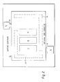
- the two outer contact areas of the metallisation pattern 13 on the diamond substrate 12 are elongated and enlarged at one end so as to extend beyond the lateral edges of the semiconductor body containing the active devices, as shown in Figure 2, to provide contact pads 14, 15.
- the three metallization areas 17,18,19 which provide the low impedance second contacts of the devices are formed in the same manner as Schottky barrier contacts, they are in fact forward-biased in operation and thus perform as low-impedance contacts.
- the presence of the n + high conductivity layer 5 through which the low-resistance contact is made to each device, is optional, but is preferably included to further reduce the impedance of these contacts.
- FIG 3 shows symbolically, the diode combination of Figure 1(d).
- L-shaped rnetallization areas 23,24 may be provided on their facing surfaces prior to bonding. These metallization areas may conveniently be formed during the same metallization steps used to form the Schottky contacts 6 and contact pads 10 on the surface of the active layer 4, and the metallization pattern 13 on the cooperating surface of the diamond substrate 12, and are then bonded together during the thermocompression bonding of the semiconductor structure to the diamond support substrate.
- the method illustrated comprises epitaxially growing a high conductivity n layer, 30 in Figure 4(a), on the surface of high quality active layer, 31, of n-type GaAs capable of supporting diode operation.
- the active layer is supported on a temporary substrate, 32, consisting of a thin epitaxial buffer layer, 33, of GaAlAs supported on a relatively thick layer, 34, of GaAs.
- a number of Schottky barrier contacts, 35, are formed on the layer, 30, and constitute the first of the two device terminals.
- the temporary substrate layers, 34 and 33 are then renoved using a selective etch tochnique as outlined for the diode combination of Figures 1 and 2 and the active layer, 31, then etched to give the required thickness. This is followed by formation of Schottky barrier contacts, 38, ( Figure 4(b)) on the resulting free surface of the active layer opposite the contacts, 35, the contacts, 38, constituting the second of the two device terminals.
- the layers 30 and 31 are then etched to give isolated regions, 39, ( Figure 4(c)) sandwiched between the first and second device terminals, the resulting structure, 40, forming a first precursor for the final diode combination.
- Figure 5 is the electrical representation of the completed device of Figure 4(d).
- a variation on the above method according to the second aspect of the invention would be to etch mesas into the layers 30 and 31 before formation of the Schottky barrier contacts, 35, instead of etching the layers to give isolated regions after formation of the contacts, 38.
- isolated regions may be etched into layer 30 and 31 after removal of the temporary substrate, 32, and before formation of the contacts, 38.
- Some of the advantages of the method according to the second aspect of the invention over the method according to the first aspect of the invention are, firstly, that there is less stray capacity associated with the interconnection metallisa- tions as the proton-isolated GaAs is replaced by air. Secondly, no proton isolation is required. This results in one less major step in the fabrication procedure of GaAs devices and allows the possibility of series connection of diodes fabricated from semiconductors which cannot be electrically isolated by this method. Thirdly, the completed diode combination is more compact as the interconnection metallizations are planar as opposed to inter-level.
- Planar metallizations also avoid the problems associated with inter-level connections over mesa edges formed by orientation-selective etchants which leave elevated sections with inwardly sloping edges. Fourthly, the design readily lends itself to heat sinking from both sides of the active layers.
- the high quality semiconductor layer providing the device active regions may be epitaxially grown on a temporary Si substrate which is selectively etchable against the active layer.
- the temporary silicon substrate may advantageously comprise a two layer structure consisting of a relatively thick first layer and a relatively thin epitaxial second layer on which the active layer is grown. If the first layer is of a different conductivity type, or has a different dopant concentration to the first layer then it may be selectively chemically or electrochemically etched against the second layer. Similarly, if the second layer is of different conductivity type, or has a different dopant concentration to the adjacent active layer, then it may also be selectively etched away against the active layer using a chemical or electrochemical etching process.
- rectifying junction may be provided by a Schottky barrier junction, or, where this is not possible or undesirable, other forms of rectifying junction contacts may alternatively be used.
- the active layer of high quality semiconductor material in which the device active regions are provided may be initially formed of high-resistivity or semi-insulating semiconductor material, and the individual device active regions then defined by selective doping of this layer, enabling different dopants and different carrier concentrations to be used in each device.
- Whichever method is used to isolate the active regions of the devices, it may be carried out either before or after removal of the temporary substrate, ie from either side of the semiconductor layer in which the active regions are formed. Similarly, formation of the holes 8 in the procedure according to Figure 1 through this layer may be performed either before or after removal of the temporary substrate, and either before or after the active regions have been defined.
- the reverse-biased rectifying junction contacts may be provided on either side of the active layer.
- the reverse-biased rectifying Schottky barrier contacts may be formed first before removal of the temporary substrate, or alternatively, the low-resistance contacts may be formed first on the surface of the epitaxial layer opposite the temporary substrate, the active rectifying junction contacts then being formed after removal of the temporary substrate.
- the resistance of the low-resistance contacts may be improved in known manner, as in the described embodiment, by forming them through a thin high conductivity (n + ) surface region provided either by doping the surface of the active layer to which contact is to be made, or by separately growing the required high conductivity layer at an appropriate stage in the process.
- n + thin high conductivity
- the quality of the contacts may also be improved by the formation of a thin high conductivity surface regions on one or both sides of the active layer before formation of the contacts.
Abstract
Description
- This invention relates to series-connected combinations of two-terminal semiconductor devices, such as microwave diodes, and to methods of fabricating such combinations on a common substra.te.
- It is well known that the amount of power that can be obtained from a microwave diode whether operating in the avalanche effect or transferred electron effect mode, is determined by the active area of the device -'the greater.this area, the more power obtainable. However, as the active area of the device is increased to obtain increased power, the capacitance of the device also increases, and this in turn causes a reduction in the impedance of the device, which varies inversely with the capacitance. If the impedance of the device becomes too small, difficulties arise in matching it with the impedance of associated circuitry, and to overcome this difficulty, it is known to connect a number of individual devices together in series tc obtain the required power while maintaining an acceptable value of impedance for the combination.
- Hitherto this has usually been done by connecting together a number of individually packaged devices resulting in a relatively bulky combination, and requiring individual interconnections between the devices to be carried out manually eg by soldering or welding.
- It is an object of the present invention to provide means whereby the above-mentioned disadvantages may be overcome or at least substantially reduced.
- According to a first aspect of the present invention a method of fabricating a series-connected combination of two-terminal semiconductor devices on a common substrate comprises:
- forming a layer of high quality semi-conductor material on the surface of a temporary substrate to provide achve qreas for the devices;
- forming first contact pattern conductors on the free surface of the high quality semiconductor layer to provide a separate first contact to this layer for each of the devices;
- bonding an insulating support substrate to the first contact pattern;
- removing the temporary substrate;
- forming second contact pattern conductors on the other surface of the high quality layer to provide a separate second contact to this layer for each of the devices;
- removing regions of the high quality layer separating the conductors of a pattern at any stage after beginning formation of the first contact pattern in order to define the device active areas so that parts of the first contact pattern are exposed when both the beer removed, temporary substrate and the regions of the high quality layer have
- and providing interconnections between the exposed parts of the first contact pattern and parts of the second contact pattern, whereby to connect the devices together in series.
- Preferably the support substrate according to the first aspect of this invention is formed on its surface with ametallic pattern to which the first contact pattern is bonded before removal of the temporary substrate.
- In the method according to the first aspect of the invention, the first contact pattern is preferably formed in two stages, the first stage providing discrehe contacts for each of the devices defining the active area thereof, and the individual active regions of the device then being isolated from one another by exposing the active layer to an ion beam using these contacts as a mask to create areas of semi-insulating material in the active layer surrounding each of the device active regions underlying the contacts. The second stage of the formation of the first contact pattern then comprises formation of a contact pad portion for each of the device first contacts which are to be interconnected with a device second contact, each of these contact pad portions overlying at least part of the associated first contact, and an adjacent area of the ion beam isolated region of the active layer. Either following removal of the temporary substrate, or before carrying out the second stage in the .formation of the first contact pattern, preferably the latter, part of the ion beam isolated region of the active layer over which the contact pad portions are formed, is removed, to enable the interconnections between the contact patterns on opposite sides of the active layer to be made following removal of the temporary substrate, the removed parts of the active layer being isolated from the device active regions.
- Alternatively, the isolation of the device active regions may be performed after removal of the temporary substrate, these regions being defined by the second contact pattern which is thus used as a mask for the isolation process. The interconnections between the contact pad portions associated with the device first contacts and the contacts of the second contact pattern are formed by an additional metallization pattern.
- According to a second aspect of the present inventio a method of fabricating a series-connected combination of two-terminal semiconductor devices on a common substrate comprises:
- fabricating a first precursor by the following procedure:
- forming a layer of high quality semiconductor material on the surface of a temporary substrate,
- forming first contact pattern conductors on the free surface of the high quality semiconductor layer to provide a separate first contact to this layer for the devices thereon,
- bonding an insulating support substrate overlayed by a conducting interconnection pattern to the first contact pattern so as to provide contact between the first and the interconnection patterns,
- removing the temporary substrate, forming second contact pattern conductors the other surface of the high quality layer to provide a separate second contact to this layer for the devices thereon,
- removing part of the high quality layer to form isolated regions in the high quality semiconductor material sandwiched between the first and second contact patterns,
- fabricating a second precursor by the same procedure as that used for the first precursor,
- bonding the first and second precursors together so as to provide contact between the second contact pattern of the one and the interconnection contact pattern of the other.
- The isolated regions of high quality semiconductor material are preferably formed according to the second aspect of the invention by removing the surrounding semiconductor material by etching. The etching may be performed immediately prior to A or after formation of the first contact pattern by creating mesas in the high quality layer or alternatively immediately prior to formation of the second contact pattern instead of after second contact pattern formation. However, if etching is performed with a contact pattern present on the free surface of the high quality layer, this pattern may advantageously serve as an etch mask.
- In order to achieve good uniformity of device characteristics, the high quality semiconductor material of both precursors according to the second aspect of the invention are preferably formed in a single step which produces a single layer; this layer then being scribed and broken into parts for each precursor.
- According to a preferred method in accordance with both aspects of the invention, the high quality layer is formed of active semiconductor material having suitable semiconductor properties capable of supporting device operation and the support substrate is formed of an electrically insulating material having a high thermal conductivity.
- Preferably at least the region of the temporary substrate immediately adjacent to the high quality layer according to both aspects of the invention is removed by selective etching using an etchant to which the high quality layer is resistant. Conveniently, the substrate may comprise a first relatively thick layer of semiconductor material formed on its surface with a relatively thin buffer layer of semiconductor material on which the high quality active layer is formed, eg by epitaxial growth, the relatively thick substrate layer then preferably being removed by a selective etching procedure to which the buffer layer is resistant, followed by removal of the buffer layer using a second selective etching procedure to which the high quality layer is resistant.
- Such a two-layer temporary substrate may comprise a relatively thick layer of GaAs and a thin epitaxial buffer layer of GaAlAs with a high quality semiconductor layer of GaAs. Alternatively, the high quality layer may be of another semi- conductor material, such as silicon, epitaxially formed on a temporary substrate having a suitable selectively etchable single or multilayer structure.
- The invention enables a number of individual two-terminal devices, such as microwave diodes, to be connected together in series at chip-level, ie in a single integrated circuit, resulting in a considerable reduction in size and in the spacing between adjacent devices providing advantages at high frequencies. The invention also avoids the need for individual packaging of the devices thereby avoiding parasitics associated with such packaging, and the reliability of the interconnections between the devices can be improved as the devices do not need to be individually bonded as in conventional series-connected arrangements. Further, because all the devices of the series combination can be formed from the same active layer, and more importantly from closely adjacent areas of the same active layer, greater diode uniformity is achieved, and increased yields can be obtained.
- The invention also extends to series connected combinations of two terminal devices fabricated by a method as aforesaid.
- The invention will now be described in greater detail, by way of example only, with reference to the accompanying drawings, of which:
- Figures 1(a) to 1(d) show in schematic cross-sectional elevation, four stages in the fabrication of a series-connected combination of microwave GaAs Impatt diodes in accordance with the first aspect of the present invention; and
- Figure 2 is a schematic plan view of the series-connected combination of microwave diodes of Figure 1.
- Figure 3 is a symbolic representation of the diode combination of Figure 1(d).
- Figures 4(a) to 4(d) show in schematic cross-sectional elevation, four stages in the fabrication of a series-connected combination of diodes in accordance with a second aspect of the invention.
- Figure 5 is a symbolic representation of the diode combination of Figure 4(d).
- Referring to Figure 1, the method illustrated comprises epitaxially growing a high conductivity n+ layer 5 approximately 1 micron thick and having a dopant concentration of about 1 x 10¹⁸ carriers/cm3 on the surface of a
temporary substrate 1 comprising a relatively thick (typically several hundred microns)layer 2 of GaAs formed with anepitaxial buffer layer 3 of GaAlAs having a thickness of about 0.5 to 2 microns. An active layer 4 of n-type GaAs, capable of supporting Impatt device operation, is then epitaxially grown on the surface of the n+ layer 5, the active layer having a thickness of about 1 micron and a dopant concentration of about 1 x 10¹⁷ carriers/cm3. The above parameters are suitable for Impatt device operation at about 50 to 60 GIIz. Because thetemporary substrate 1 forms no part of the completed device, and because the relatively thick GaAs layer thereof is isolated from the layers 4 and 5 by thebuffer layer 3, its electrical properties are unimportant. The GaAs layer of the substrate may thus be of any suitable conductivity type, eg n,p or semi-insulating (SI). - Following formation of the active layer 4, a number (4 in this example) of Schottky
barrier contacts 6, one more than the number of devices of the required series-connected combination, are formed on the free surface of the active layer 4, defining the active area of each device. Thecontacts 6 are formed by initially applying a sputtered or evaporated metallization pattern, suitably of Ti/Au, which is then electrolytically plated with a 1 to 2 micron thick layer of Au (Fig 1(a)). The size of each contact is typically about 50 x 20 microns. - These contacts, which provide the first of the two device terminals are then used as a mask in an ion beam isolation process in which the slice is irradiated with a beam of high energy protons to convert all regions of the layers 4 and 5 which are not covered by the
contacts 6, into semi-insulating form. The energy of the proton beam is progressively increased in known manner, in 100 keV intervals until the penetration depth extends just into theunderlying buffer layer 3, thus ensuring that the exposed regions of the active layer 4 and underlying portions of the n+ layer 5 are isolated throughout their thickness. The process results in a separateactive region 7 of n-type GaAs underlying each of the Schottkycontacts 6 surrounded by proton isolated semi-insulating GaAs material. - Following the isolation of the
active device regions 7, part of the proton-isolated layers 4 and 5 is removed using a photolithographically formed resist mask to defineholes 8 extending through to theunderlying buffer layer 3, one between each pair ofcontacts 6, but separated therefrom by a region of the proton-isolated active layer. These holes are formed using a selective. etchant, for example a 95.5 mixture of100V H 202 and 35% NH4OH, which will automatically stop at the interface between the layer 5 and the underlyingGaAlAs buffer layer 3 which is resistant to this etchant; as shown in Fig 1(b). - A second metallization pattern is then formed to connect respective ones of the three of the four Schottky
contacts 6 to the adjacent one of theholes 8. The pattern thus comprises aseparate area 9 overlying each of thecontacts 6, which, in the case of the threecontacts 6 which are to be connected with one of theholes 8, also extends into a'contactpad portion 10 overlying theadjacent hole 8 to one side of the associatedcontact 6 as shown in Figure 1(c). This second metallization stage is again formed by first applying an evaporated or sputtered metallisation pattern of, for example, Ti/Au, which is then electrolytically plated-up with Au to a thickness of about 1 to 2 microns. - The next stage in the process comprises bonding an insulating
support substrate 12 of high thermal conductivity material to theelevated metallization areas 9. As shown, thesupport substrate 12 comprises a diamond chip (commercially available Type IIa diamond chips are preferred) having the desired insulating and high thermal conductivity properties. To facilitate the bonding process, the surface of thediamond chip 12 is formed with an evaporated or sputteredmetallization pattern 13, eg of Ti/Au or Cr/Au corresponding to that of thecontacts 6. Themetallization pattern 13 on thediamond substrate 12 is aligned with theelevated metallization areas 9 on the semiconductor structure, and the two are then bonded together in known manner, suitably using a thermo-compression bonding technique. The device at this stage is shown in Fig 1(c). - Having affixed the semiconductor structure to the support substrate, the
temporary substrate 1 is then removed using a two-stage selective etching process. The first stage comprises removal of thethick GaAs layer 2 using an etchant to which the GaAlAs buffer layer is resistant, and the active layer 4 being suitably protected. A suitable etchant is a 95:5 mixture of 100V H2O2 and 35% NH4OH, which will automatically stop at the interface between theGaAs layer 2 and theGaAlAs buffer layer 3. Thethin buffer layer 3 is then removed using a selective etchant to which the layer 5 is resistant, suitably a 50% solution of HF in water. This etch can thus be made to automatically stop at the interface between theGaAlAs buffer layer 3 and the GaAs n+ layer 5, to leave a thin highly uniform epitaxially formed layer of GaAs supported by thesupport substrate 12, and exposing those areas of thecontact pad portions 10 previously formed on the other side of the active layer 4 Which overlay theholes 8 formed in the proton isolated regions of the active layer. - A surface thickness of the epitaxial GaAs layer immediately underlying the
GaAlAs buffer layer 3, which in this example comprises the surface of the n+ GaAs layer 5, may then be removed to reduce this layer to any desired thickness, and to remove any surface impurities. This step may be of greater importance in devices in which the GaAlAs buffer layer is interfaced directly with the epitaxial active layer 4, ie where the n+ layer 5 is omitted, or is formed on the opposite side of layer 4. - A further metallization pattern, again conveniently formed by initially applying on evaporated or sputtered pattern of Ti/Au which is then plated-up to a thickness of about '1 to 2 microns, is then formed on the free surface of the semiconductor structure to complete the series interconnection of three of the four devices of the combination while also providing the second contact terminal for each of tthese three devices. This pattern thus comprises three
separate areas contact pad portion 10 of the second device of the series which is exposed through thehole 8 between the first and second devices. This metallisation area thus provides an interconnection between the low-impedance second contact terminal of the first device and the Schottky barrierfirst contact terminal 6 of the second device. - Similarly the
second metallization area 18 provides the low resistance second contact terminal for the second device of the series, and provides an interconnection between this contact terminal and the Schottky barrierfirst contact 6 of the third device of the series via thecontact pad 10 associated with thiscontact 6. Finally, thethird metallisation area 19 provides the.low resistance second contact terminal for the third device of the series and serves to provide an interconnection between this contact terminal and theSchottky barrier contact 6 of the fourth unused device structure of the series. In fact this fourth device structure forms no operational part of the completed device combination, and is formed solely to enable the external connection to be made to this end of the completed combination at the surface of the diamond support substrate rather than directly to the low impedancesecond contact terminal 19 of the third device of the series. This is because bonding directly to contact terminals supported directly on the thin semoconductor layer in which the devices are formed may damage or harmfully affect the properties of this layer. - To provide contact areas for external connection to each end of the series combination, the two outer contact areas of the
metallisation pattern 13 on thediamond substrate 12 are elongated and enlarged at one end so as to extend beyond the lateral edges of the semiconductor body containing the active devices, as shown in Figure 2, to providecontact pads - It will be noted that although the three
metallization areas - Figure 3 shows symbolically, the diode combination of Figure 1(d).
- To improve the mechanical stability of the thin GaAs device structure on the
support substrate 12 additional L-shapedrnetallization areas 23,24 (Figure 2) may be provided on their facing surfaces prior to bonding. These metallization areas may conveniently be formed during the same metallization steps used to form theSchottky contacts 6 andcontact pads 10 on the surface of the active layer 4, and themetallization pattern 13 on the cooperating surface of thediamond substrate 12, and are then bonded together during the thermocompression bonding of the semiconductor structure to the diamond support substrate. - In Figure 4 the method illustrated comprises epitaxially growing a high conductivity n layer, 30 in Figure 4(a), on the surface of high quality active layer, 31, of n-type GaAs capable of supporting diode operation. The active layer is supported on a temporary substrate, 32, consisting of a thin epitaxial buffer layer, 33, of GaAlAs supported on a relatively thick layer, 34, of GaAs. A number of Schottky barrier contacts, 35, (two are illustrated in Figure 4+(a)) are formed on the layer, 30, and constitute the first of the two device terminals. An insulating support substrate, 36, of high thermal conductivity (diamond in this example) and overlaid on its surface by interconnection metallization areas, 37, which correspond with the contacts, 35, is bonded to the n+ layer so that the areas, 37, and the contacts, 35, are sealed together.
- The temporary substrate layers, 34 and 33, are then renoved using a selective etch tochnique as outlined for the diode combination of Figures 1 and 2 and the active layer, 31, then etched to give the required thickness. This is followed by formation of Schottky barrier contacts, 38, (Figure 4(b)) on the resulting free surface of the active layer opposite the contacts, 35, the contacts, 38, constituting the second of the two device terminals. The
layers - Figure 5 is the electrical representation of the completed device of Figure 4(d).
- A variation on the above method according to the second aspect of the invention would be to etch mesas into the
layers layer - Some of the advantages of the method according to the second aspect of the invention over the method according to the first aspect of the invention are, firstly, that there is less stray capacity associated with the interconnection metallisa- tions as the proton-isolated GaAs is replaced by air. Secondly, no proton isolation is required. This results in one less major step in the fabrication procedure of GaAs devices and allows the possibility of series connection of diodes fabricated from semiconductors which cannot be electrically isolated by this method. Thirdly, the completed diode combination is more compact as the interconnection metallizations are planar as opposed to inter-level. Planar metallizations also avoid the problems associated with inter-level connections over mesa edges formed by orientation-selective etchants which leave elevated sections with inwardly sloping edges. Fourthly, the design readily lends itself to heat sinking from both sides of the active layers.
- Although the invention has been described in its application to the fabrication of four series-connected diodes, it may equally be applied to the fabrication of any number of series-connected two-terminal semiconductor devices of other types, using GaAs or other suitable materials for which selective etching processes are known such as InP or Si.
- For example, in the application of the invention to Si devices, the high quality semiconductor layer providing the device active regions may be epitaxially grown on a temporary Si substrate which is selectively etchable against the active layer. The temporary silicon substrate may advantageously comprise a two layer structure consisting of a relatively thick first layer and a relatively thin epitaxial second layer on which the active layer is grown. If the first layer is of a different conductivity type, or has a different dopant concentration to the first layer then it may be selectively chemically or electrochemically etched against the second layer. Similarly, if the second layer is of different conductivity type, or has a different dopant concentration to the adjacent active layer, then it may also be selectively etched away against the active layer using a chemical or electrochemical etching process. By providing a relatively thin second, or buffer, layer on the temporary Si substrate against the active layer, very thin active layers of high uniformity can be achieved. Suitable chemical and electrochemical etching techniques are described in Theunissem et al "Application of Preferential Electrochemical Etching of Silicon to Semiconductor Device Technology" J,Electrochem,Society, Electrochemical Technology, Vol 117, No. 7, July 1970, pages 959 to 965, in C P Wen et al "Preferential Electrochemical Etching of P Silicon in an - Aqueous HF - H2S04 Electrolyte" J Electrochem Soc. Vol 119, April 1972, No 4 pp 547 - 478; in C J Rhee et al "Integral Heat - Sink Impatt Diodes Fabricated using P Etch Stop". Proc IEEE Vol 61, No 3 p 385 - 387 March 1973; and in V Kern "Chemical Etching of Si, Ge, GaAs and GaP". RCA Review June 1978,
Vol 39, pages 278 to 308. - Of course, in devices in which at least one of the two terminal contacts must be provided by a rectifying junction, this may be provided by a Schottky barrier junction, or, where this is not possible or undesirable, other forms of rectifying junction contacts may alternatively be used.
- Furthermore, other modifications to the particular fabrication procedure described above may be made without departing from the scope of the present invention. For example, the active layer of high quality semiconductor material in which the device active regions are provided may be initially formed of high-resistivity or semi-insulating semiconductor material, and the individual device active regions then defined by selective doping of this layer, enabling different dopants and different carrier concentrations to be used in each device.
- Whichever method is used to isolate the active regions of the devices, it may be carried out either before or after removal of the temporary substrate, ie from either side of the semiconductor layer in which the active regions are formed. Similarly, formation of the
holes 8 in the procedure according to Figure 1 through this layer may be performed either before or after removal of the temporary substrate, and either before or after the active regions have been defined. - In the application of the invention to avalanche effect devices, in which one of the two contacts of each device is a reverse-biased rectifying junction contact, eg a reverse-biased Schottky barrier contact as in the described embodiment, and the other is a low resistance contact, the reverse-biased rectifying junction contacts may be provided on either side of the active layer. The reverse-biased rectifying Schottky barrier contacts may be formed first before removal of the temporary substrate, or alternatively, the low-resistance contacts may be formed first on the surface of the epitaxial layer opposite the temporary substrate, the active rectifying junction contacts then being formed after removal of the temporary substrate. Whichever arrangement is selected, the resistance of the low-resistance contacts may be improved in known manner, as in the described embodiment, by forming them through a thin high conductivity (n+) surface region provided either by doping the surface of the active layer to which contact is to be made, or by separately growing the required high conductivity layer at an appropriate stage in the process. Similarly, in the case of transferred electron effect devices, such as Gunn Diodes, in which both contacts of each device are low-impedance contacts, the quality of the contacts may also be improved by the formation of a thin high conductivity surface regions on one or both sides of the active layer before formation of the contacts.
Claims (17)
Applications Claiming Priority (2)
| Application Number | Priority Date | Filing Date | Title |
|---|---|---|---|
| GB7939564 | 1979-11-15 | ||
| GB7939564 | 1979-11-15 |
Publications (2)
| Publication Number | Publication Date |
|---|---|
| EP0029334A1 true EP0029334A1 (en) | 1981-05-27 |
| EP0029334B1 EP0029334B1 (en) | 1984-04-04 |
Family
ID=10509219
Family Applications (1)
| Application Number | Title | Priority Date | Filing Date |
|---|---|---|---|
| EP80304027A Expired EP0029334B1 (en) | 1979-11-15 | 1980-11-11 | Series-connected combination of two-terminal semiconductor devices and their fabrication |
Country Status (5)
| Country | Link |
|---|---|
| US (1) | US4339870A (en) |
| EP (1) | EP0029334B1 (en) |
| JP (1) | JPS56124274A (en) |
| CA (1) | CA1150852A (en) |
| DE (1) | DE3067381D1 (en) |
Cited By (18)
| Publication number | Priority date | Publication date | Assignee | Title |
|---|---|---|---|---|
| EP0069511B1 (en) * | 1981-06-25 | 1985-11-21 | Itt Industries, Inc. | Fabricating integrated circuits |
| EP0293629A2 (en) * | 1987-06-04 | 1988-12-07 | Licentia Patent-Verwaltungs-GmbH | Method of manufacture of a semiconductor device with contact on both sides |
| EP0472451A1 (en) * | 1990-08-21 | 1992-02-26 | Thomson-Csf | Hybrid integrated circuit interconnection structure and method of fabrication |
| WO1993011562A1 (en) * | 1991-12-06 | 1993-06-10 | Picogica S.A. | Method of making semiconductor components with electrochemical recovery of the substrate |
| WO1993011559A1 (en) * | 1991-12-06 | 1993-06-10 | Picogiga S.A. | METHOD FOR MANUFACURING SEMICONDUCTER COMPONENTS, PARTICULARLY ON GaAs OR InP, WITH CHEMICAL RECOVERY OF THE SUBSTRAT |
| US5403729A (en) * | 1992-05-27 | 1995-04-04 | Micro Technology Partners | Fabricating a semiconductor with an insulative coating |
| EP0665586A1 (en) * | 1994-01-31 | 1995-08-02 | Philips Electronics Uk Limited | Manufacture of electronic devices comprising thin-film circuits |
| US5455187A (en) * | 1988-11-21 | 1995-10-03 | Micro Technology Partners | Method of making a semiconductor device with a metallic layer coupled to a lower region of a substrate and metallic layer coupled to a lower region of a semiconductor device |
| WO1995026569A1 (en) * | 1992-05-27 | 1995-10-05 | Micro Technology Partners | Fabricating a semiconductor with an insulative coating |
| GB2289372A (en) * | 1994-05-10 | 1995-11-15 | Nissan Motor | Method of manufacturing ohmic contact |
| US5521420A (en) * | 1992-05-27 | 1996-05-28 | Micro Technology Partners | Fabricating a semiconductor with an insulative coating |
| EP0692821A3 (en) * | 1994-07-11 | 1996-08-07 | Mitsubishi Electric Corp | Method of manufacturing semiconductor layer |
| US5557149A (en) * | 1994-05-11 | 1996-09-17 | Chipscale, Inc. | Semiconductor fabrication with contact processing for wrap-around flange interface |
| US5827751A (en) * | 1991-12-06 | 1998-10-27 | Picogiga Societe Anonyme | Method of making semiconductor components, in particular on GaAs of InP, with the substrate being recovered chemically |
| EP0977252A1 (en) * | 1998-07-30 | 2000-02-02 | Commissariat A L'energie Atomique | Selective transfer of elements from one support to another support |
| US6121119A (en) * | 1994-06-09 | 2000-09-19 | Chipscale, Inc. | Resistor fabrication |
| FR2793953A1 (en) * | 1999-05-21 | 2000-11-24 | Thomson Csf | Electronic component, especially a microwave HBT useful for air traffic control radar equipment, has device layer stacks and similar pads for heat conduction from a flat top heat dissipation element to a bottom substrate |
| US6355981B1 (en) | 1997-01-24 | 2002-03-12 | Chipscale, Inc. | Wafer fabrication of inside-wrapped contacts for electronic devices |
Families Citing this family (23)
| Publication number | Priority date | Publication date | Assignee | Title |
|---|---|---|---|---|
| US5144413A (en) * | 1981-11-23 | 1992-09-01 | Raytheon Company | Semiconductor structures and manufacturing methods |
| FR2536908B1 (en) * | 1982-11-30 | 1986-03-14 | Telecommunications Sa | METHOD FOR MANUFACTURING A MATRIX INFRARED DETECTOR WITH LIGHTING FROM THE FRONT PANEL |
| US4596069A (en) * | 1984-07-13 | 1986-06-24 | Texas Instruments Incorporated | Three dimensional processing for monolithic IMPATTs |
| US4596070A (en) * | 1984-07-13 | 1986-06-24 | Texas Instruments Incorporated | Interdigitated IMPATT devices |
| US4695861A (en) * | 1985-10-21 | 1987-09-22 | Honeywell Inc. | Backside mosaic photoconductive infrared detector array |
| JPS62194652A (en) * | 1986-02-21 | 1987-08-27 | Hitachi Ltd | Semiconductor device |
| US4894114A (en) * | 1987-02-11 | 1990-01-16 | Westinghouse Electric Corp. | Process for producing vias in semiconductor |
| US4747908A (en) * | 1987-04-09 | 1988-05-31 | Microelectronics and Computer Technologogy Corporation | Method of making a hermetically sealed multilayer electrical feedthru |
| US4896205A (en) * | 1987-07-14 | 1990-01-23 | Rockwell International Corporation | Compact reduced parasitic resonant frequency pulsed power source at microwave frequencies |
| JPH0344067A (en) * | 1989-07-11 | 1991-02-25 | Nec Corp | Laminating method of semiconductor substrate |
| US5309003A (en) * | 1992-02-28 | 1994-05-03 | At&T Bell Laboratories | Article comprising a real space transfer semiconductor device, and method of making the article |
| US5236871A (en) * | 1992-04-29 | 1993-08-17 | The United States Of America As Represented By The Administrator Of The National Aeronautics And Space Administration | Method for producing a hybridization of detector array and integrated circuit for readout |
| US5385632A (en) * | 1993-06-25 | 1995-01-31 | At&T Laboratories | Method for manufacturing integrated semiconductor devices |
| JP2669413B2 (en) * | 1995-09-28 | 1997-10-27 | 日本電気株式会社 | Electronic component mounting structure |
| US5627112A (en) * | 1995-11-13 | 1997-05-06 | Rockwell International Corporation | Method of making suspended microstructures |
| JPH11150185A (en) * | 1997-11-14 | 1999-06-02 | Nippon Steel Corp | Manufacture of semiconductor device |
| JP4465745B2 (en) * | 1999-07-23 | 2010-05-19 | ソニー株式会社 | Semiconductor laminated substrate, semiconductor crystal substrate, semiconductor element, and manufacturing method thereof |
| US6287891B1 (en) * | 2000-04-05 | 2001-09-11 | Hrl Laboratories, Llc | Method for transferring semiconductor device layers to different substrates |
| US6730990B2 (en) * | 2000-06-30 | 2004-05-04 | Seiko Epson Corporation | Mountable microstructure and optical transmission apparatus |
| EP1215721B1 (en) * | 2000-12-13 | 2008-01-23 | Infineon Technologies AG | Process for multistep processing of a thin and brittle Wafer |
| CN100401535C (en) * | 2004-01-07 | 2008-07-09 | 洲磊科技股份有限公司 | Method for forming light-emitting diode with metal base plate |
| KR101536306B1 (en) * | 2008-10-24 | 2015-07-14 | 동국대학교 산학협력단 | Fabrication method of the 2 terminal semiconductor devices using trench technology |
| US9633982B2 (en) * | 2015-02-17 | 2017-04-25 | Chun Yen Chang | Method of manufacturing semiconductor device array |
Citations (5)
| Publication number | Priority date | Publication date | Assignee | Title |
|---|---|---|---|---|
| FR2023722A1 (en) * | 1968-11-20 | 1970-08-21 | Matsushita Electronics Corp | |
| US3986196A (en) * | 1975-06-30 | 1976-10-12 | Varian Associates | Through-substrate source contact for microwave FET |
| FR2373879A1 (en) * | 1976-12-07 | 1978-07-07 | Thomson Csf | Mesa type diode semiconductor structure - has reduced mesa part and has highly doped residual substrate of small thickness |
| US4106052A (en) * | 1975-04-19 | 1978-08-08 | Semikron Gesellschaft Fur Gleichrichterbau Und Elektronik M.B.H. | Semiconductor rectifier unit having a base plate with means for maintaining insulating wafers in a desired position |
| GB2004416A (en) * | 1977-09-14 | 1979-03-28 | Raytheon Co | Semiconductor device |
Family Cites Families (11)
| Publication number | Priority date | Publication date | Assignee | Title |
|---|---|---|---|---|
| US3489961A (en) * | 1966-09-29 | 1970-01-13 | Fairchild Camera Instr Co | Mesa etching for isolation of functional elements in integrated circuits |
| JPS5012995B1 (en) * | 1970-02-09 | 1975-05-16 | ||
| US3649881A (en) * | 1970-08-31 | 1972-03-14 | Rca Corp | High-power semiconductor device assembly |
| US3721593A (en) * | 1971-08-13 | 1973-03-20 | Motorola Inc | Etch stop for koh anisotropic etch |
| US4189342A (en) * | 1971-10-07 | 1980-02-19 | U.S. Philips Corporation | Semiconductor device comprising projecting contact layers |
| JPS49131863U (en) * | 1973-03-10 | 1974-11-13 | ||
| US3902095A (en) * | 1973-10-09 | 1975-08-26 | Raytheon Co | Electron beam semiconductor amplifier with shielded diode junctions |
| GB1480592A (en) * | 1973-11-02 | 1977-07-20 | Marconi Co Ltd | Light emitting diodes |
| US3979820A (en) * | 1974-10-30 | 1976-09-14 | General Electric Company | Deep diode lead throughs |
| US3959045A (en) * | 1974-11-18 | 1976-05-25 | Varian Associates | Process for making III-V devices |
| US4241360A (en) * | 1978-08-10 | 1980-12-23 | Galileo Electro-Optics Corp. | Series capacitor voltage multiplier circuit with top connected rectifiers |
-
1980
- 1980-11-11 DE DE8080304027T patent/DE3067381D1/en not_active Expired
- 1980-11-11 EP EP80304027A patent/EP0029334B1/en not_active Expired
- 1980-11-13 US US06/206,680 patent/US4339870A/en not_active Expired - Lifetime
- 1980-11-14 CA CA000364699A patent/CA1150852A/en not_active Expired
- 1980-11-15 JP JP16012680A patent/JPS56124274A/en active Pending
Patent Citations (5)
| Publication number | Priority date | Publication date | Assignee | Title |
|---|---|---|---|---|
| FR2023722A1 (en) * | 1968-11-20 | 1970-08-21 | Matsushita Electronics Corp | |
| US4106052A (en) * | 1975-04-19 | 1978-08-08 | Semikron Gesellschaft Fur Gleichrichterbau Und Elektronik M.B.H. | Semiconductor rectifier unit having a base plate with means for maintaining insulating wafers in a desired position |
| US3986196A (en) * | 1975-06-30 | 1976-10-12 | Varian Associates | Through-substrate source contact for microwave FET |
| FR2373879A1 (en) * | 1976-12-07 | 1978-07-07 | Thomson Csf | Mesa type diode semiconductor structure - has reduced mesa part and has highly doped residual substrate of small thickness |
| GB2004416A (en) * | 1977-09-14 | 1979-03-28 | Raytheon Co | Semiconductor device |
Cited By (36)
| Publication number | Priority date | Publication date | Assignee | Title |
|---|---|---|---|---|
| EP0069511B1 (en) * | 1981-06-25 | 1985-11-21 | Itt Industries, Inc. | Fabricating integrated circuits |
| EP0293629A2 (en) * | 1987-06-04 | 1988-12-07 | Licentia Patent-Verwaltungs-GmbH | Method of manufacture of a semiconductor device with contact on both sides |
| EP0293629A3 (en) * | 1987-06-04 | 1990-02-28 | Licentia Patent-Verwaltungs-GmbH | Method of manufacture of a semiconductor device with contact on both sides |
| US4959328A (en) * | 1987-06-04 | 1990-09-25 | Licentia Patent-Verwaltungs-Gmbh | Method for manufacturing a semiconductor component contactable on both sides |
| US5789817A (en) * | 1988-11-21 | 1998-08-04 | Chipscale, Inc. | Electrical apparatus with a metallic layer coupled to a lower region of a substrate and a metallic layer coupled to a lower region of a semiconductor device |
| US5455187A (en) * | 1988-11-21 | 1995-10-03 | Micro Technology Partners | Method of making a semiconductor device with a metallic layer coupled to a lower region of a substrate and metallic layer coupled to a lower region of a semiconductor device |
| US5262351A (en) * | 1990-08-21 | 1993-11-16 | Thomson-Csf | Process for manufacturing a multilayer integrated circuit interconnection |
| EP0472451A1 (en) * | 1990-08-21 | 1992-02-26 | Thomson-Csf | Hybrid integrated circuit interconnection structure and method of fabrication |
| FR2666173A1 (en) * | 1990-08-21 | 1992-02-28 | Thomson Csf | HYBRID INTERCONNECTION STRUCTURE FOR INTEGRATED CIRCUITS AND MANUFACTURING METHOD. |
| US5827751A (en) * | 1991-12-06 | 1998-10-27 | Picogiga Societe Anonyme | Method of making semiconductor components, in particular on GaAs of InP, with the substrate being recovered chemically |
| FR2684801A1 (en) * | 1991-12-06 | 1993-06-11 | Picogiga Sa | PROCESS FOR PRODUCING SEMICONDUCTOR COMPONENTS, ESPECIALLY ON GAAS OR INP, WITH CHEMICAL RECOVERY OF THE SUBSTRATE. |
| WO1993011562A1 (en) * | 1991-12-06 | 1993-06-10 | Picogica S.A. | Method of making semiconductor components with electrochemical recovery of the substrate |
| WO1993011559A1 (en) * | 1991-12-06 | 1993-06-10 | Picogiga S.A. | METHOD FOR MANUFACURING SEMICONDUCTER COMPONENTS, PARTICULARLY ON GaAs OR InP, WITH CHEMICAL RECOVERY OF THE SUBSTRAT |
| US5593917A (en) * | 1991-12-06 | 1997-01-14 | Picogiga Societe Anonyme | Method of making semiconductor components with electrochemical recovery of the substrate |
| FR2684800A1 (en) * | 1991-12-06 | 1993-06-11 | Picogiga Sa | PROCESS FOR THE REALIZATION OF SEMICONDUCTOR COMPONENTS WITH RECOVERY OF SUBSTRATE BY ELECTROCHEMICAL METHOD. |
| US5592022A (en) * | 1992-05-27 | 1997-01-07 | Chipscale, Inc. | Fabricating a semiconductor with an insulative coating |
| US5521420A (en) * | 1992-05-27 | 1996-05-28 | Micro Technology Partners | Fabricating a semiconductor with an insulative coating |
| US5403729A (en) * | 1992-05-27 | 1995-04-04 | Micro Technology Partners | Fabricating a semiconductor with an insulative coating |
| WO1995026569A1 (en) * | 1992-05-27 | 1995-10-05 | Micro Technology Partners | Fabricating a semiconductor with an insulative coating |
| US5444009A (en) * | 1992-05-27 | 1995-08-22 | Micro Technology Partners | Fabricating a semiconductor with an insulative coating |
| US5441898A (en) * | 1992-05-27 | 1995-08-15 | Micro Technology Partners | Fabricating a semiconductor with an insulative coating |
| EP0665586A1 (en) * | 1994-01-31 | 1995-08-02 | Philips Electronics Uk Limited | Manufacture of electronic devices comprising thin-film circuits |
| US5476810A (en) * | 1994-01-31 | 1995-12-19 | U.S. Philips Corporation | Manufacture of electronic devices comprising thin-film circuits using a metal foil as a temporary support |
| GB2289372A (en) * | 1994-05-10 | 1995-11-15 | Nissan Motor | Method of manufacturing ohmic contact |
| GB2289372B (en) * | 1994-05-10 | 1998-08-19 | Nissan Motor | Method of manufacturing semiconductor device |
| US5557149A (en) * | 1994-05-11 | 1996-09-17 | Chipscale, Inc. | Semiconductor fabrication with contact processing for wrap-around flange interface |
| US5656547A (en) * | 1994-05-11 | 1997-08-12 | Chipscale, Inc. | Method for making a leadless surface mounted device with wrap-around flange interface contacts |
| US6121119A (en) * | 1994-06-09 | 2000-09-19 | Chipscale, Inc. | Resistor fabrication |
| EP0692821A3 (en) * | 1994-07-11 | 1996-08-07 | Mitsubishi Electric Corp | Method of manufacturing semiconductor layer |
| US6355981B1 (en) | 1997-01-24 | 2002-03-12 | Chipscale, Inc. | Wafer fabrication of inside-wrapped contacts for electronic devices |
| EP0977252A1 (en) * | 1998-07-30 | 2000-02-02 | Commissariat A L'energie Atomique | Selective transfer of elements from one support to another support |
| FR2781925A1 (en) * | 1998-07-30 | 2000-02-04 | Commissariat Energie Atomique | SELECTIVE TRANSFER OF ELEMENTS FROM ONE MEDIUM TO ANOTHER MEDIUM |
| US6204079B1 (en) | 1998-07-30 | 2001-03-20 | Commissariat A L'energie Atomique | Selective transfer of elements from one support to another support |
| FR2793953A1 (en) * | 1999-05-21 | 2000-11-24 | Thomson Csf | Electronic component, especially a microwave HBT useful for air traffic control radar equipment, has device layer stacks and similar pads for heat conduction from a flat top heat dissipation element to a bottom substrate |
| WO2000072379A1 (en) * | 1999-05-21 | 2000-11-30 | Thomson-Csf | Thermal capacity for electronic component operating in long pulses |
| US6559534B1 (en) | 1999-05-21 | 2003-05-06 | Thomson-Csf | Thermal capacity for electronic component operating in long pulses |
Also Published As
| Publication number | Publication date |
|---|---|
| CA1150852A (en) | 1983-07-26 |
| DE3067381D1 (en) | 1984-05-10 |
| US4339870A (en) | 1982-07-20 |
| EP0029334B1 (en) | 1984-04-04 |
| JPS56124274A (en) | 1981-09-29 |
Similar Documents
| Publication | Publication Date | Title |
|---|---|---|
| US4339870A (en) | Series-connected two-terminal semiconductor devices and their fabrication | |
| US3986196A (en) | Through-substrate source contact for microwave FET | |
| KR101004720B1 (en) | Field effect transistor, semiconductor chip, and semiconductor device | |
| US5449930A (en) | High power, compound semiconductor device and fabrication process | |
| US6440822B1 (en) | Method of manufacturing semiconductor device with sidewall metal layers | |
| US5455187A (en) | Method of making a semiconductor device with a metallic layer coupled to a lower region of a substrate and metallic layer coupled to a lower region of a semiconductor device | |
| US3509433A (en) | Contacts for buried layer in a dielectrically isolated semiconductor pocket | |
| WO1989006444A2 (en) | Vertical power transistor and fabrication methods | |
| US3878553A (en) | Interdigitated mesa beam lead diode and series array thereof | |
| US5145809A (en) | Fabrication of gunn diode semiconductor devices | |
| US4596070A (en) | Interdigitated IMPATT devices | |
| US4127830A (en) | Microstrip switch wherein diodes are formed in single semiconductor body | |
| US6127716A (en) | Heterojunction bipolar transistor and manufacturing method thereof | |
| US3397450A (en) | Method of forming a metal rectifying contact to semiconductor material by displacement plating | |
| US4596069A (en) | Three dimensional processing for monolithic IMPATTs | |
| CN116705844A (en) | Semiconductor structure and forming method thereof | |
| US4238763A (en) | Solid state microwave devices with small active contact and large passive contact | |
| EP0314712B1 (en) | Two-terminal semiconductor diode arrangement | |
| US5457068A (en) | Monolithic integration of microwave silicon devices and low loss transmission lines | |
| US4023258A (en) | Method of manufacturing semiconductor diodes for use in millimeter-wave circuits | |
| US5512776A (en) | Interdigitated IMPATT devices | |
| US4095330A (en) | Composite semiconductor integrated circuit and method of manufacture | |
| US5418181A (en) | Method of fabricating diode using grid recess | |
| US4143384A (en) | Low parasitic capacitance diode | |
| JPH07107940B2 (en) | Shoutoki Barrier diode device |
Legal Events
| Date | Code | Title | Description |
|---|---|---|---|
| PUAI | Public reference made under article 153(3) epc to a published international application that has entered the european phase |
Free format text: ORIGINAL CODE: 0009012 |
|
| AK | Designated contracting states |
Designated state(s): DE FR GB IT NL |
|
| 17P | Request for examination filed |
Effective date: 19811001 |
|
| ITF | It: translation for a ep patent filed |
Owner name: BARZANO' E ZANARDO ROMA S.P.A. |
|
| GRAA | (expected) grant |
Free format text: ORIGINAL CODE: 0009210 |
|
| AK | Designated contracting states |
Designated state(s): DE FR GB IT NL |
|
| REF | Corresponds to: |
Ref document number: 3067381 Country of ref document: DE Date of ref document: 19840510 |
|
| ET | Fr: translation filed | ||
| PLBE | No opposition filed within time limit |
Free format text: ORIGINAL CODE: 0009261 |
|
| STAA | Information on the status of an ep patent application or granted ep patent |
Free format text: STATUS: NO OPPOSITION FILED WITHIN TIME LIMIT |
|
| 26N | No opposition filed | ||
| PG25 | Lapsed in a contracting state [announced via postgrant information from national office to epo] |
Ref country code: NL Effective date: 19850601 |
|
| GBPC | Gb: european patent ceased through non-payment of renewal fee | ||
| NLV4 | Nl: lapsed or anulled due to non-payment of the annual fee | ||
| PG25 | Lapsed in a contracting state [announced via postgrant information from national office to epo] |
Ref country code: FR Free format text: LAPSE BECAUSE OF NON-PAYMENT OF DUE FEES Effective date: 19850731 |
|
| PG25 | Lapsed in a contracting state [announced via postgrant information from national office to epo] |
Ref country code: DE Effective date: 19850801 |
|
| REG | Reference to a national code |
Ref country code: FR Ref legal event code: ST |
|
| PG25 | Lapsed in a contracting state [announced via postgrant information from national office to epo] |
Ref country code: GB Effective date: 19881118 |