EP0035740A1 - Capacitive sensor for a time-piece and method of manufacturing this sensor - Google Patents
Capacitive sensor for a time-piece and method of manufacturing this sensor Download PDFInfo
- Publication number
- EP0035740A1 EP0035740A1 EP81101528A EP81101528A EP0035740A1 EP 0035740 A1 EP0035740 A1 EP 0035740A1 EP 81101528 A EP81101528 A EP 81101528A EP 81101528 A EP81101528 A EP 81101528A EP 0035740 A1 EP0035740 A1 EP 0035740A1
- Authority
- EP
- European Patent Office
- Prior art keywords
- substrate
- static sensor
- metallization
- sensor according
- dielectric
- Prior art date
- Legal status (The legal status is an assumption and is not a legal conclusion. Google has not performed a legal analysis and makes no representation as to the accuracy of the status listed.)
- Granted
Links
Images


Classifications
-
- G—PHYSICS
- G04—HOROLOGY
- G04G—ELECTRONIC TIME-PIECES
- G04G21/00—Input or output devices integrated in time-pieces
- G04G21/08—Touch switches specially adapted for time-pieces
-
- H—ELECTRICITY
- H03—ELECTRONIC CIRCUITRY
- H03K—PULSE TECHNIQUE
- H03K17/00—Electronic switching or gating, i.e. not by contact-making and –breaking
- H03K17/94—Electronic switching or gating, i.e. not by contact-making and –breaking characterised by the way in which the control signals are generated
- H03K17/96—Touch switches
- H03K17/962—Capacitive touch switches
-
- Y—GENERAL TAGGING OF NEW TECHNOLOGICAL DEVELOPMENTS; GENERAL TAGGING OF CROSS-SECTIONAL TECHNOLOGIES SPANNING OVER SEVERAL SECTIONS OF THE IPC; TECHNICAL SUBJECTS COVERED BY FORMER USPC CROSS-REFERENCE ART COLLECTIONS [XRACs] AND DIGESTS
- Y10—TECHNICAL SUBJECTS COVERED BY FORMER USPC
- Y10S—TECHNICAL SUBJECTS COVERED BY FORMER USPC CROSS-REFERENCE ART COLLECTIONS [XRACs] AND DIGESTS
- Y10S200/00—Electricity: circuit makers and breakers
- Y10S200/02—Body attached switches
Definitions
- the present invention relates to a static sensor for a timepiece comprising at least two juxtaposed capacitive effect electrodes, sensitive to touch and activated manually, and electronic means for detecting each position of the finger which corresponds at least to a symbol which can take the form a particular number, letter or sign.
- Static capacitive sensors are known from the state of the art. In certain applications, they advantageously replace mechanical push-buttons and they are found, for example, in elevator control systems, in programming sewing machines and for controlling the various functions of an electronic watch, such as resetting the time or choosing a specific function.
- an interactive data input device for a timepiece comprising a static sensor formed by the juxtaposition of N electrodes delivering at their output at least N - 1 coded information representative of the position of the finger on the sensor, characterized in that it comprises means for generating signals representative of the data which it is sought to select or modify, means for displaying said symbol on a composite display and means for detecting the direction and the speed of the finger on the sensor. If the cited request describes in detail the electronic arrangement of such a device, it says nothing about the practical realization of the captive keys and how to incorporate them into the timepiece.
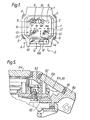
- Figure 1 is a top view of the timepiece according to the invention. It comprises a box 1 in which are mounted an electronic module of which the display 2 can be seen, a plurality 3, 4, 5, 6 and 7 of push buttons and a static sensor 100 which is the subject of the present invention and which will be described in detail later.
- the display 2 which can be formed by a liquid crystal cell, comprises, in addition to the permanent display 8 of the standard time made up of three groups of two digits displaying the hours 9, the minutes 10 and the seconds 11, an auxiliary display 12 which can display for example the day of the week 13, the month 14 and the date 15. Signs 16, permanently fixed and for example transferred under the watch glass signa slow the possible operating modes in which the auxiliary display can be switched.
- the sign AG 1 means “agenda 1" and the sign D the "date”.
- the display of a frame 17 indicates in which mode one is.
- the patent application cited above describes in detail how, by means of the sensor 100, the main display is set to the time, the operating mode is selected and new data is introduced into the auxiliary display.
- FIG. 2 is a section along line A - A through the sensor of Figure 1 and on an enlarged scale.
- the sensor 100 comprises an electrically insulating substrate 30, a first metallization 101, a second metallization 32, connection means 33 between said first and second metallizations, an electrically insulating compensation layer 34, a dielectric 35 and a decorative layer 36.
- second metallization 32 directly carries the electronic means (not shown in FIG. 2) necessary for the operation of the sensor as well as its output terminals (not visible in FIG. 2).
- the insulating substrate 30 constitutes the base of the sensor.
- the choice of its material and its preparation will depend its ability to fulfill the performance expected of it, that is to say, a strong, impact resistance that may occur when wearing the watch.
- sapphire In addition to its high intrinsic resistance, sapphire also has the advantage of withstanding the high temperatures necessary for laying the coatings discussed below. Glass for example, in addition to its great brittleness, would soften in the presence of temperatures of the order of 800 to 1000 ° C.
- the substrate is obtained by sawing in a direction such that the axis C of the hexagonal crystal mesh lies in the plane of said substrate.
- the holes 37 are laser drilled. It should be noted here that this method is one of the only con coming from such a hard and thick material (of the order of a millimeter). It normally results in a diameter d l of a small hole (of the order of 0.1 mm) relative to the thickness d 2. Of the substrate, which is advantageous since it will then be a matter of plugging it by means dielectric 35 as will be explained later. In a preferred version of the invention, the ratio of the thickness d2 to the diameter d l is arranged in such a way that the relation d 2 / d 1 > 4 is satisfied.
- the substrate receives a stabilization heat treatment after which the holes are finally chamfered at 38.
- the scratches which appeared at the birth of the holes are removed by a new running-in.
- the substrate is polished fine on its two large surfaces. It has been found that this polishing is essential for the solidity of the substrate and contributes, by suppressing the incipient fractures which scratches might have, to very clearly improve its impact resistance. To achieve the desired performance and according to experience, the average roughness after polishing will not exceed 0.05 ⁇ m (optical polish).
- FIG. 3 shows an example of the geometry of the first metallization 101 of the substrate, on the outside of the timepiece.
- a conductive paste which may contain, for example, a mixture of palladium, platinum and silver. Whatever paste is chosen, it is essential that it adapts well to the successive covering operations which will be described and above all that it develops excellent adhesion to the polished surface of the substrate.
- the paste known commercially under the name EMCA 7157 A satisfies these requirements well.
- the geometry of this deposit consists of four electrodes of square shape 101.
- the thick layer thus deposited is baked at a temperature between 800 and 1000 ° vs.
- the constitution of the screen-printing screen and the consistency of the paste are chosen so that the thickness of the metallization after baking is between 5 and 15 ⁇ m.
- FIG. 4 shows an example of the geometry of the second metallization 32 of the substrate, on the interior side of the timepiece.
- the deposition takes place, as for the deposition of the electrodes, by screen printing according to the same preferential requirements of paste composition, baking temperature and metallization thickness after baking.
- the same suction is created through the holes 37 but from the outer face of the substrate this time to ensure electrical continuity between the two metal layers.
- the configuration of the second metallization as it appears in FIG. 4 shows various conductors capable of receiving the: electronic means suitable for detecting the position of the finger on the sensor as well as input and output terminals of said sensor. The description will repeat this particular arrangement later.
- the first and second metallizations are not limited to a screen printing process.
- Other known means could be used such as, for example, depositing thin layers under vacuum, the essential being, at least for the second metallization, that the thickness of the conductors is compatible with the ultrasonic connection of gold or aluminum wires (bonding), with tin-lead solder and with bonding using conductive epoxy adhesive.
- a compensation layer 34 which is visible in the section of FIG. 2.
- This electrically insulating layer 34 will be applied by screen printing, baked in the oven at a temperature between 800 and 1000 ° C. Its thickness after firing must be the same as that of the electrodes, that is to say between 5 and 15 m. It should be mentioned here that one could very well deposit the compensation layer 34 before metallization 101. As for the metallization layer, the compensation layer must have excellent adhesion to the polished substrate. The paste known in the trade under the name EMCA 2828 B satisfies this requirement well.
- FIG. 2 also shows that the metallization 101 and the compensation layer 34 are surmounted by a dielectric 35.
- This deposition is carried out by screen printing in at least two passes of an insulating paste.
- this layer must have a suitable relative dielectric constant ⁇ r, of value between 8 and 16, it must also ensure perfect sealing between the front face and the rear face of the sensor.
- the first pass will opt the four metallized holes 37 at the same time as it will cover the entire front face. After drying at around 125 ° C, it still has microscopic pores which will be covered by the second pass in order to protect the electrodes against humidity and ensure perfect opturation of the metallized holes.
- the wafer is baked in the oven at a temperature between 800 and 1000 ° C.
- the thickness of the dielectric after baking will preferably be between 20 and 100 ⁇ m.
- the dielectric must also have good adhesion to the layers on which it is deposited. A paste similar to that used for the compensation layer meets this requirement well.
- FIG. 2 finally shows that the dielectric layer 35 which has just been described is in turn overcome by a decorative layer 36.
- this decorative layer is deposited by screen printing.
- a porcelain enamel which will be fired at a temperature between 770 and 850 ° C.
- This type of enamel much more resistant than baking paint (300 ° C) or glass enamel ( ⁇ 620 ° C), is very hard and resists abrasion well.
- the decorative layer can be applied all at once (one color) or several times (two colors and more).
- An example of decoration in two colors appears in Figure 1 where we find in 40 a white color and in 41 a black decorative pattern which includes a long line embraced by a sign - and by a + sign which mean that the group of digits to be corrected will decrease in value if the finger moves towards the sign - or on the contrary will increase in value if the finger moves towards the + sign.
- the decorative layer 36 also acts as a dielectric layer since it is superimposed on the main dielectric layer 35. It will therefore be important that its thickness after firing (5 to 20 f m approximately), its relative dielectric constant & .r (between 6.5 and 13) and its electrical insulating properties are chosen judiciously so as not to destroy the capacitive effect obtained by the main dielectric.
- a static sensor is therefore now available which, according to a preferred version of the invention, has four capacitive effect electrodes. If the watch wearer touches the decorative layer 36 in the area of an electrode 101 with a finger, the capacitance of the capacitor formed with the mass of the metal case is modified, the finger being part of the mass armature and being separated from the electrode 101 by the dielectric constituted by the layers 35 and 36. It is therefore possible to use this variation in capacity to produce a control signal when the upper face of the sensor is touched by the finger, and thus to produce a sensor capacitive based on this effect.
- this capacitive sensor is arranged in series with a condenser or fixed injection capacity 64 to form a capacitive divider connected on the one hand to ground (armature constituted by the finger) , on the other hand to a terminal 105 of an alternating voltage generator delivering for example a signal at 32 kHz.
- the voltage at the point of connection of the electrode 101 to a frame 103 of the injection capacitor 64 is: representative of the fact that the electrode 101 is subject to a command or not.
- the second metallization 32 serves as conductors for directly carrying the electronic means for detecting the position of the finger on the sensor and of the input and output terminals. tie of said sensor. Said electronic means are described in FIG. 3 of the patent application already cited EP 80107773.6.
- the transcoder 104 and the assembly 113 of this figure are assembled in a single integrated circuit which is placed as indicated in FIG. 4 of the present invention.
- the mass of the circuit is bonded by means of a conductive adhesive to the field 61 itself connected to the supply terminal +.
- the output of the circuit giving the direction of movement of the finger is connected to terminal 109a and the fast and slow outputs intended to influence one or the other display group, depending on whether the finger moves quickly or slowly on the sensor.
- Terminal 62 is made active with a single touch of the finger on the sensor and allows for example the zeroing of seconds or the stopping of an alarm signal.
- Terminal - is the negative input of the power supply and terminal 63, the signal input at 32 kHz.
- the electrodes 101 shown in FIG. 3 are electrically connected to the conductors 103 by the metallized holes 37. These conductors 103 are the same as those which appear under the same reference in FIG. 3 of the application for patent cited.
- the fixed injection capacitors 64 which have been mentioned above, as well as the conductors 103 and 105 are connected to the integrated circuit as illustrated in FIG. 4.
- the terminals of the injection capacitors 64 can be soldered or glued by means of conductive epoxy adhesive to the conductors 103, 105, the metallization 32 serving both as a support and as a fixing for these capacitors.
- These capacitors can be discrete added components, but it would be possible to integrate them entirely or in part according to known methods directly in the circuit 104, 113.
- the integrated circuit 104, 113 is bonded to the various conductors which surround it. Once this operation has been carried out, it is encapsulated according to known techniques. To delimit the encapsulation zone and thus prevent material from reaching unwanted locations, a thick frame 65 (40 to 200 ⁇ m) is deposited on the second metallization 32 by screen printing or by any other technique. suitable.
- Figure 5 is a partial section on an enlarged scale along the free B - B of Figure 1. It shows how the sensor is incorporated in the timepiece.
- the sensor 100 is driven into the middle 80 in the manner of a watch crystal by means of a seal 81. Under the sensor we can see the encapsulated circuit 104, 113.
- the conductors 109a, 124a, 125a, 62 , +, -, 63 presented in FIG. 4 are connected to the circuits 85 for use and display of the watch by means of a flexible multiple connector 82 of the "zebra" type that the sleeve 83 prevents from bending.
- the senor 100 is completely separated from the glass 84.
- the present invention is not limited to this arrangement. Indeed, if the crystal is of the sapphire type (which would therefore meet the requirements posed by the production of the sensor according to the invention), a second zone of this crystal could be used, apart from the first which normally covers the display. , to implement the sensor described here.
- the capacitive sensor is waterproof as usual glass, and like it, withstands the shocks and mechanical, physical and chemical stresses which normally arise in the environment of a wristwatch. We have also seen that the sensor constitutes a compact unit which can be produced in large series, checked for itself and then very simply mounted in the middle of the watch.
Abstract
Description
La présente invention concerne un capteur statique pour pièce d'horlogerie comportant au moins deux électrodes à effet capacitif juxtaposées, sensibles au toucher et activées manuellement et des moyens électroniques pour détecter chaque position du doigt qui correspond au moins à un symbole qui peut prendre la forme d'un chiffre, d'une lettre ou d'un signe particulier.The present invention relates to a static sensor for a timepiece comprising at least two juxtaposed capacitive effect electrodes, sensitive to touch and activated manually, and electronic means for detecting each position of the finger which corresponds at least to a symbol which can take the form a particular number, letter or sign.
Des capteurs statiques à effet capacitif sont connus de l'état de la technique. Dans certaines applications, ils remplacent avantageusement des boutons-poussoirs mécaniques et on les trouve, par exemple, dans des systèmes de commande d'ascenseur, dans la programmation de machines à coudre et pour commander les diverses fonctions d'une montre électronique, telles que la remise à l'heure ou le choix d'une fonction bien précise.Static capacitive sensors are known from the state of the art. In certain applications, they advantageously replace mechanical push-buttons and they are found, for example, in elevator control systems, in programming sewing machines and for controlling the various functions of an electronic watch, such as resetting the time or choosing a specific function.
Dans le cas de l'utilisation d'un tel capteur en horlogerie on comprendra l'intérêt qu'il présente sur un poussoir mécanique qui doit traverser le boîtier pour être accessible de l'extérieur et qui, de ce fait, amène des problèmes d'étanchéité et de pollution entraînant une augmentation des coûts de fabrication et une diminution de 1a fiabilité du système de commande. Il faut mentionner aussi que l'encombrement d'un capteur statique peut être réduit à des dimensions nettement inférieures à celles d'un poussoir mécanique traditionnel.In the case of the use of such a sensor in watchmaking, it will be understood the advantage which it presents on a mechanical pusher which must pass through the case in order to be accessible from the outside and which, therefore, causes problems of sealing and pollution resulting in increased manufacturing costs and decreased reliability of the control system. It should also be mentioned that the size of a static sensor can be reduced to dimensions much smaller than those of a traditional mechanical pusher.
Dans sa demande de brevet EP 80107773.6,.la requérante propose un dispositif interactif d'entrée de données pour pièce d'horlogerie comportant un capteur statique formé par la juxtaposition de N électrodes délivrant à leur sortie au moins N - 1 informations codées représentatives de la position du doigt sur le capteur caractérisé par le fait qu'il comprend des moyens pour générer des signaux représentatifs des données qu'on cherche à sélectionner ou à modifier, des moyens pour afficher ledit symbole sur un affichage composite et des moyens pour détecter le sens et la vitesse du doigt sur le capteur. Si la demande citée décrit en détail l'arrangement électronique d'un tel dispositif, elle ne dit rien sur la réalisation pratique des touches captrices et sur la façon de les incorporer dans la pièce d'horlogerie.In its patent application EP 80107773.6, the applicant proposes an interactive data input device for a timepiece comprising a static sensor formed by the juxtaposition of N electrodes delivering at their output at least N - 1 coded information representative of the position of the finger on the sensor, characterized in that it comprises means for generating signals representative of the data which it is sought to select or modify, means for displaying said symbol on a composite display and means for detecting the direction and the speed of the finger on the sensor. If the cited request describes in detail the electronic arrangement of such a device, it says nothing about the practical realization of the captive keys and how to incorporate them into the timepiece.
C'est le but de la présente invention de proposer une construction originale comportant la juxtaposition d'au moins deux électrodes, construction qui satisfasse au bon fonctionnement du dispositif interactif d'entrée de données de la demande citée.It is the aim of the present invention to propose an original construction comprising the juxtaposition of at least two electrodes, construction which satisfies the proper functioning of the interactive data entry device of the cited request.
C'est un autre but de l'invention de proposer un dispositif compact facile à produire en grandes séries, de dimensions réduites, qui incorpore non seulement lés touches capacitives mais encore le circuit électronique assurant son fonctionnement..It is another object of the invention to provide a compact device easy to produce in large series, of reduced dimensions, which incorporates not only the capacitive keys but also the electronic circuit ensuring its operation.
C'est encore un autre but de l'invention de réaliser un capteur sensitif d'aspect plaisant et décoratif, étanche et particulièrement résistant aux sollicitations mécaniques, physiques et chimiques que l'on trouve dans l'environnement habituel d'une montre-bracelet.It is yet another object of the invention to produce a sensitive sensor with a pleasant and decorative appearance, waterproof and particularly resistant to mechanical, physical and chemical stresses which are found in the usual environment of a wristwatch. .
Ces buts sont atteints grâce aux moyens revendiqués.These goals are achieved by the means claimed.
L'invention sera comprise maintenant à la lumière de la description qui suit donnée à titre d'exemple et à l'aide du dessin dans lequel :
- La figure 1 est une vue de dessus de la pièce d'horlogerie dans laquelle apparaît l'affichage et un capteur statique indépendant dudit affichage.
- La figure 2 est une coupe selon la ligne A - A à travers le capteur de la figure 1 et à échelle agrandie.
- La figure 3 montre la métallisation du capteur, côté extérieur de la pièce d'horlogerie.
- La figure 4 montre la métallisation du capteur, côté intérieur de la pièce d'horlogerie.
- La figure 5 est une coupe partielle à échelle agrandie selon la ligne B - B de la figure 1 et qui montre comment le capteur est incorporé dans la pièce d'horlogerie.
- Figure 1 is a top view of the timepiece in which the display appears and a static sensor independent of said display.
- Figure 2 is a section along line A - A through the sensor of Figure 1 and on an enlarged scale.
- Figure 3 shows the metallization of the sensor on the outside of the timepiece.
- Figure 4 shows the metallization of the sensor on the inside of the timepiece.
- Figure 5 is a partial section on an enlarged scale along line B - B of Figure 1 and which shows how the sensor is incorporated in the timepiece.
La figure 1 est une vue de dessus de la pièce d'horlogerie selon l'invention. Elle comporte une boîte 1 dans laquelle sont montés un module électronique dont on aperçoit l'affichage 2, une pluralité 3, 4, 5, 6 et 7 de boutons-poussoirs et un capteur statique 100 objet de la présente invention et qui sera décrit en détail plus loin. L'affichage 2, qui peut être formé d'une cellule à cristal liquide, comprend, outre l'affichage permanent 8 de l'heure normale composée de trois groupes de deux chiffres affichant les heures 9, les minutes 10 et les secondes 11, un affichage auxiliaire 12 qui peut afficher par exemple le jour de la semaine 13, le mois 14 et la date 15. Des signes 16, fixés à demeure et par exemple décalqués sous la glace de la montre signalent les modes de fonctionnement possibles dans lesquels on peut commuter l'affichage auxiliaire. Par exemple, le signe AG 1 signifie "agenda 1" et le signe D la "date". L'affichage d'un encadrement 17 signale dans quel mode on se trouve. La demande de brevet citée plus haut décrit en détail comment, au moyen du capteur 100, on met à l'heure l'affichage principal, on sélectionne le mode de fonctionnement et l'on introduit des données nouvelles dans l'affichage auxiliaire.Figure 1 is a top view of the timepiece according to the invention. It comprises a box 1 in which are mounted an electronic module of which the
La description qui va suivre concerne le capteur statique 100, sa composition et les procédés mis en oeuvre pour sa fabrication selon l'invention.The description which follows relates to the
La figure 2 est une coupe selon la ligne A - A à travers le capteur de la figure 1 et à échelle agrandie. Le capteur 100 comprend un substrat électriquement isolant 30, une première métallisation 101, une seconde métallisation 32, des moyens de liaisons 33 entre lesdites première et seconde métallisations, une couche de compensation électriquement isolante 34, un diélectrique 35 et une couche décorative 36. La seconde métallisation 32 porte directement les moyens électroniques (non représentés sur la figure 2) nécessaires au fonctionnement du capteur ainsi que ses bornes de sortie (non visibles en figure 2).Figure 2 is a section along line A - A through the sensor of Figure 1 and on an enlarged scale. The
Les diverses parties entrant dans la composition du capteur vont être décrites maintenant en détail.The various parts involved in the composition of the sensor will now be described in detail.
Le substrat isolant 30 constitue la base du capteur. Du choix de sa matière et de sa préparation dépendra son aptitude à remplir les performances qu'on attend de lui, c'est-à-dire une forte, résistance aux chocs qui peuvent se présenter lors du porter de la montre. C'est le saphir qui, selon l'invention, a été trouvé le plus apte à remplir cette fonction. En plus de sa résistance intrinsèque élevée, le saphir a encore l'avantage de supporter les hautes températures nécessaires à la pose des revêtements dont il sera question plus bas. Du verre par exemple, outre sa grande fragilité, se ramollirait en présence de températures de l'ordre de 800 à 1000 °C. Le substrat est obtenu par sciage selon une direction telle que l'axe C de la maille cristalline hexagonale se trouve dans le plan dudit substrat. Il subit ensuite une opération usuelle de mise en forme (par exemple rectangulaire ou tra- pézotdale) et de rodage des surfaces. Les trous 37 sont percés au laser. Il faut signaler ici que cette méthode est l'une des seules convenables à un matériau si dur et si épais (de l'ordre du millimètre). Elle aboutit normalement à un diamètre dl de trou petit (de l'ordre de 0,1 mm) par rapport à l'épaisseur d2.du substrat, ce qui est avantageux car il s'agira de l'obturer ensuite au moyen du diélectrique 35 comme cela sera expliqué plus loin. Dans une version préférée dé l'invention, le rapport dé l'épaisseur d2 au diamètre dl est arrangé de telle façon que la relation d2 / d1 > 4 soit satisfaite. Le substrat reçoit un traitement thermique de stabilisation après quoi les trous sont enfin chanfreinés en 38. Les égrisures qui sont apparues à la naissance des trous sont supprimées par un nouveau rodage. Enfin le substrat est poli fin sur ses deux grandes surfaces. On a trouvé que ce polissage est capital pour la solidité du substrat et contribue., en supprimant les amorces de rupture- que pourraient présenter des rayures, à améliorer très nettement sa résistance aux chocs. Pour attein- dre la performance souhaitée et selon l'expérience, la rugosité moyenne après polissage ne dépassera pas 0,05 µm (poli optique).The
D'autres matériaux peuvent remplacer avec succès le saphir car ils répondent également aux critères de résistance énoncés plus haut et l'invention s'étend à des substrats comme le spinelle, le rubis, le quartz et la silice amorphe.Other materials can successfully replace sapphire because they also meet the resistance criteria stated above and the invention extends to substrates such as spinel, ruby, quartz and amorphous silica.
Sur le substrat préparé comme indiqué plus haut, il est possible alors de déposer la première métallisation 101, puis la seconde métallisation 32, la métallisation 33 du trou 37 se réalisant en même temps comme on va le voir.On the substrate prepared as indicated above, it is then possible to deposit the
La figure 3 montre un exemple de géométrie de la première métallisation 101 du substrat, côté extérieur de la pièce d'horlogerie. Sur la face extérieure du substrat 30 on dépose, de préférence par sérigraphie, une pâte conductrice qui peut contenir par exemple un mélange de palladium, de platine et d'argent. Quelle que soit la pâte choisie, il est essentiel qu'elle s'adapte bien aux opérations successives de recouvrement qui vont être décrites et surtout qu'elle développe une excellente adhérence sur la surface polie du substrat. La pâte connue dans le commerce sous la dénomination EMCA 7157 A satisfait bien à ces exigences. La géométrie de ce dépôt consiste en quatre électrodes de forme carrée 101. Pendant le dépôt de la pâte, on crée une aspiration à travers les trous 37 à partir de la face opposée à celle de la figure, ce qui, additionné à un phénomène naturel de capillarité, contribue à faire pénétrer la pâte à l'intérieur des trous et former sur au moins une demi-longueur de ceux-ci la métallisation 33. Puis la couche épaisse ainsi déposée est cuite au four à une température comprise entre 800 et 1000 °C. La constitution de l'écran sérigraphique, la consistance de la pâte sont choisies de telle façon que l'épaisseur de la métallisation après cuisson soit comprise entre 5 et 15 µm.FIG. 3 shows an example of the geometry of the
La figure 4 montre un exemple de géométrie de la seconde métallisation 32 du substrat, côté intérieur de la pièce d'horlogerie. Le dépôt a lieu, comme pour le dépôt des électrodes, par sérigraphie selon les mêmes exigences préférentielles de composition de pâte, de température de cuisson et d'épaisseur de métallisation après cuisson. Pendant l'application de la pâte on crée la même aspiration à travers les trous 37 mais depuis la face extérieure du substrat cette fois-ci pour assurer la continuité électrique entre les deux couches métalliques. La configuration de la seconde métallisation telle qu'elle apparaît en figure 4 fait apparaître divers conducteurs aptes à recevoir les : moyens électroniques propres à détecter la position du doigt sur le capteur ainsi que des bornes d'entrée et de sortie dudit capteur. La description reprendra plus loin cet arrangement particulier.FIG. 4 shows an example of the geometry of the
Les première et seconde métallisations ne se limitent pas à un procédé sérigraphique. D'autres moyens connus pourraient être utilisés comme, par exemple, le dépôt de couches minces sous vide, l'essentiel étant, pour la seconde métallisation tout au moins, que l'épaisseur des conducteurs soit compatible avec la connexion par ultra-son de fils d'or ou d'aluminium (bonding), avec la soudure étain - plomb et avec le collage au moyen de colle époxy conductrice.The first and second metallizations are not limited to a screen printing process. Other known means could be used such as, for example, depositing thin layers under vacuum, the essential being, at least for the second metallization, that the thickness of the conductors is compatible with the ultrasonic connection of gold or aluminum wires (bonding), with tin-lead solder and with bonding using conductive epoxy adhesive.
Si l'on se réfère à nouveau à la figure 3, on voit qu'il existe des espaces libres 60 entre les électrodes 101. Si l'on veut que la surface finale du capteur soit absolument plane, il est nécessaire de combler ces espaces au moyen d'une couche de compensation 34 qui est visible sur la coupe de la figure 2. Cette couche électriquement isolante 34 sera appliquée par dépôt sérigraphique, cuite au four à une température comprise entre 800 et 1000 °C. Son épaisseur après cuisson devra être la même que celle des électrodes, c'est-à-dire comprise entre 5 et 15 m. Il faut mentionner ici que l'on pourrait très bien déposer la couche de compensation 34 avant la métallisation 101. Comme pour la couche de métallisation, la couche de compensation devra présenter une excellente adhérence au substrat poli. La pâte connue dans le commerce sous la dénomination EMCA 2828 B satisfait bien à cette exigence.If we refer again to FIG. 3, we see that there are
La figure 2 montre encore que la métallisation 101 et la couche de compensation 34 sont surmontées d'un diélectrique 35. Ce dépôt est réalisé par sérigraphie en au moins deux passes d'une pâte isolante. Outre le fait que cette couche doit présenter une constante diélectrique relative εr convenable, de valeur comprise entre 8 et 16, elle doit encore assurer une étanchéité parfaite entre la face avant et la face arrière du capteur. La première passe opturera les quatre trous métallisés 37 en même temps qu'elle recouvrira toute la face avant. Après séchage à environ 125 °C, elle présente encore des pores microscopiques qui seront recouverts par la deuxième passe dans le but de protéger les électrodes contre l'humidité et d'assurer une opturation parfaite des trous métallisés. Une fois les deux couches appliquées, on cuit la plaquette au four à une température comprise entre 800 et 1000 °C. L'épaisseur du diélectrique après cuisson sera de préférence comprise entre 20 et 100 µm. Le diélectrique doit présenter également une bonne adhérence aux couches sur lesquelles il est déposé. Une pâte semblable à celle utilisée pour la couche de compensation répond bien à cette exigence.FIG. 2 also shows that the
A la place du dépôt par sérigraphie du diélectrique, il serait concevable d'utiliser une lame mince de saphir, de verre ou de céramique qui serait appliquée sur le substrat et la métallisation par collage ou autre procédé convenable.Instead of depositing the dielectric by screen printing, it would be conceivable to use a thin blade of sapphire, glass or ceramic which would be applied to the substrate and the metallization by bonding or other suitable process.
, Pour donner un aspect esthétique idoine à la surface apparente du capteur, la figure 2 montre enfin que la couche diélectrique 35 qui vient d'être décrite est surmontée à son tour pas une couche décorative 36. Comme pour les autres couches dont il a été question plus haut, cette couche décorative est déposée par sérigraphie. On choisira de préférence un émail pour porcelaine dont la cuisson se fera à une température comprise entre 770 et 850 °C. Ce type d'émail, beaucoup plus résistant que de la peinture à cuire (300 °C) ou de l'émail pour verre ( < 620 °C), est très dur et résiste bien à l'abrasion. Ces qualités obligent à choisir un substrat résistant aux hautes températures (saphir) comme cela a déjà été mentionné plus haut.To give an appropriate aesthetic appearance to the apparent surface of the sensor, FIG. 2 finally shows that the
La couche décorative peut être appliquée en une seule fois (une seule couleur) ou en plusieurs fois (deux couleurs et plus). Un exemple de décoration en deux couleurs apparaît en figure 1 où l'on trouve en 40 une couleur blanche et en 41 un motif décoratif noir qui comporte un long trait embrassé par un signe - et par un signe + qui veulent signifier que le groupe de chiffres à corriger diminuera de valeur si le doigt se déplace vers le signe - ou au contraire augmentera de valeur si le doigt se déplace vers le signe +.The decorative layer can be applied all at once (one color) or several times (two colors and more). An example of decoration in two colors appears in Figure 1 where we find in 40 a white color and in 41 a black decorative pattern which includes a long line embraced by a sign - and by a + sign which mean that the group of digits to be corrected will decrease in value if the finger moves towards the sign - or on the contrary will increase in value if the finger moves towards the + sign.
Il faut mentionner que la couche décorative 36 agit également comme couche diélectrique puisqu'elle est superposée à la couche diélectrique principale 35. Il sera donc important que son épaisseur après cuisson (5 à 20 fm environ), sa constante diélectrique relative &.r (comprise entre 6,5 et 13) et ses propriétés d'isolant électrique soient choisies judicieusement pour ne pas détruire l'effet capacitif obtenu par le diélectrique principal.It should be mentioned that the
On dispose donc maintenant d'un capteur statique qui comporte, selon une version préférée de l'invention, quatre électrodes à effet capacitif. Si le porteur de la montre touche avec un doigt la couche décorative 36 dans la zone d'une électrode 101, la capacité du condensateur formé avec la masse du boîtier métallique est modifiée, le doigt faisant partie de l'armature masse et étant séparé de l'électrode 101 par le diélectrique constitué par les couches 35 et 36. Il est donc possible d'utiliser cette variation de capacité pour produire un signal de commande quand la face supérieure du capteur est touchée par le doigt, et de réaliser ainsi un capteur capacitif fondé sur cet effet. Comme cela est décrit en détail dans le brevet CH 607 872, ce capteur capacitif est disposé en série avec un condensateur ou capacité d'injection fixe 64 pour former un diviseur capacitif connecté d'une part à la masse (armature constituée par le doigt), d'autre part à une borne 105 d'un générateur de tension alternative délivrant par exemple un signal à 32 kHz. Ainsi, la tension au point de raccordement de l'électrode 101 à une armature 103 du condensateur d'injection 64 est: représentative du fait que l'électrode 101 est soumise à une commande ou non.A static sensor is therefore now available which, according to a preferred version of the invention, has four capacitive effect electrodes. If the watch wearer touches the
Selon l'invention, la seconde métallisation 32 sert de conducteurs pour porter directement les moyens électroniques pour détecter la position du doigt sur le capteur et des bornes d'entrée et de sortie dudit capteur. Lesdits moyens électroniques sont décrits en figure 3 de la demande de brevet déjà citée EP 80107773.6. Le transcodeur 104 et l'ensemble 113 de cette figure sont assemblés en un seul circuit intégré qui est placé comme indiqué sur la figure 4 de la présente invention. La masse du circuit est collée au moyen d'une colle conductrice sur le champ 61 lui-même relié à la borne d'alimentation +. La sortie du circuit donnant le sens de déplacement du doigt est reliée à la borne 109a et les sorties rapide et lente destinées à influencer l'un ou l'autre groupe d'affichage, selon que le doigt se déplace rapidement ou lentement sur le capteur, sont reliées aux bornes 125a et 124a respectivement. La borne 62 est rendue active à un seul toucher du doigt sur le capteur et permet par exemple la mise à zéro des secondes ou l'arrêt d'un signal d'alarme. La borne - est l'entrée négative de l'alimentation et la borne 63, l'entrée du signal à 32 kHz. Comme on l'a déjà vu, les électrodes 101 (figurées en figure 3) sont reliées électriquement aux conducteurs 103 par les trous métallisés 37. Ces conducteurs 103 sont les mêmes que ceux qui figurent sous la même référence en figure 3 de la demande de brevet citée. Les condensateurs d'injection fixes 64, dont il a été question plus haut, ainsi que les conducteurs 103 et 105 sont reliés au circuit intégré comme illustré sur la figure 4. Les bornes des condensateurs d'injection 64 peuvent être soudées ou collées au moyen de colle êpoxy conductrice aux conducteurs 103, 105, la métallisation 32 servant à la fois de support et de fixation pour ces condensateurs. Ces condensateurs peuvent être des composants discrets rapportés, mais il serait possible de les intégrer entièrement ou en partie selon des procédés connus directement dans le circuit 104, 113.According to the invention, the
Le circuit intégré 104, 113 est relié par bonding aux divers conducteurs qui l'entourent. Une fois cette opération réalisée, on l'en- capsule selon des techniques connues. Pour délimiter la zone d'encap- sulation et éviter ainsi que de la matière n'atteigne des endroits non désirés, on dépose sur la seconde métallisation 32 un cadre 65 de forte épaisseur (40 à 200 pm) par sérigraphie ou par toute autre technique convenable.The integrated circuit 104, 113 is bonded to the various conductors which surround it. Once this operation has been carried out, it is encapsulated according to known techniques. To delimit the encapsulation zone and thus prevent material from reaching unwanted locations, a thick frame 65 (40 to 200 μm) is deposited on the
La figure 5 est une coupe partielle à échelle agrandie selon la libre B - B de la figure 1. Elle montre comment le capteur est incorporé dans la pièce d'horlogerie. Dans l'exemple de réalisation, le capteur 100 est chassé dans la carrure 80 à la manière d'une glace de montre au moyen d'une garniture d'étanchéité 81. Sous le capteur on peut voir le circuit encapsulé 104, 113. Les conducteurs 109a, 124a, 125a, 62, +, -, 63 présentés en figure 4 sont reliés aux circuits 85 d'utilisation et d'affichage de la montre au moyen d'un connecteur multiple souple 82 du type "zebra" que le manchon 83 empêche de fléchir.Figure 5 is a partial section on an enlarged scale along the free B - B of Figure 1. It shows how the sensor is incorporated in the timepiece. In the embodiment, the
Dans l'exemple de réalisation illustrée par la figure 5, le capteur 100 est totalement séparé de la glace 84. La présente invention n'est pas limitée à cette disposition. En effet, si la glace est du type saphir (ce qui répondrait donc aux exigences posées par la réalisation du capteur selon l'invention), on pourrait utiliser une seconde zone de cette glace, en dehors de la première qui recouvre normalement l'affichage, pour mettre en oeuvre le capteur ici décrit. Quelle que soit la réalisation prévue, on voit que le capteur capacitif est étanche comme une glace habituelle, et comme elle, résiste aux chocs et aux sollicitations mécaniques, physiques et chimiques qui se présentent normalement dans l'environnement d'une montre-bracelet. On a vu aussi que le capteur constitue une unité compacte qui peut être réalisée en, grandes séries, contrôlée pour elle-même puis montée très simplement dans la carrure de la montre.In the embodiment illustrated in FIG. 5, the
Claims (17)
Applications Claiming Priority (2)
| Application Number | Priority Date | Filing Date | Title |
|---|---|---|---|
| CH1796/80 | 1980-03-07 | ||
| CH1796/80A CH643978B (en) | 1980-03-07 | 1980-03-07 | STATIC SENSOR FOR WATCH PART. |
Publications (2)
| Publication Number | Publication Date |
|---|---|
| EP0035740A1 true EP0035740A1 (en) | 1981-09-16 |
| EP0035740B1 EP0035740B1 (en) | 1984-03-07 |
Family
ID=4218793
Family Applications (1)
| Application Number | Title | Priority Date | Filing Date |
|---|---|---|---|
| EP81101528A Expired EP0035740B1 (en) | 1980-03-07 | 1981-03-04 | Capacitive sensor for a time-piece and method of manufacturing this sensor |
Country Status (5)
| Country | Link |
|---|---|
| US (1) | US4435090A (en) |
| EP (1) | EP0035740B1 (en) |
| JP (2) | JPS56163480A (en) |
| CH (1) | CH643978B (en) |
| DE (1) | DE3162455D1 (en) |
Families Citing this family (6)
| Publication number | Priority date | Publication date | Assignee | Title |
|---|---|---|---|---|
| US5864518A (en) * | 1996-03-29 | 1999-01-26 | Performance General Corporation | Device and method for analyzing a swimmer's swim stroke |
| WO2000071971A1 (en) | 1999-05-24 | 2000-11-30 | Luxtron Corporation | Optical techniques for measuring layer thicknesses |
| ATE414292T1 (en) * | 2005-06-14 | 2008-11-15 | Rado Montres Sa | HOUSING CLOSED BY A GLASS WITH INVISIBLE CONNECTION OR WITH DECORATION POSSIBILITY, AND PRODUCTION METHOD THEREOF |
| US8964513B2 (en) * | 2005-06-14 | 2015-02-24 | The Swatch Group Research And Development Ltd | Technical or decorative piece associating a transparent material and a silicon based amorphous material and method of manufacturing the same |
| EP1734423B1 (en) * | 2005-06-14 | 2009-10-14 | Asulab S.A. | Fitting of a tactile glass on a watch case |
| US8599144B2 (en) * | 2006-07-31 | 2013-12-03 | Cypress Semiconductor Corporation | Grounded button for capacitive sensor |
Citations (9)
| Publication number | Priority date | Publication date | Assignee | Title |
|---|---|---|---|---|
| US3937049A (en) * | 1973-03-12 | 1976-02-10 | Citizen Watch Co., Ltd. | Monitoring system for digital electronic timepiece |
| FR2281617A1 (en) * | 1974-08-09 | 1976-03-05 | Seiko Instr & Electronics | LIQUID CRYSTAL DISPLAY DEVICE |
| FR2331831A1 (en) * | 1975-11-11 | 1977-06-10 | Seiko Instr & Electronics | ELECTRONIC WATCH |
| US4056699A (en) * | 1975-11-13 | 1977-11-01 | Essex International, Inc. | Touch plate assembly |
| US4136291A (en) * | 1977-05-23 | 1979-01-23 | General Electric Company | Capacitive touch-pad devices with dynamic bias |
| GB2009976A (en) * | 1977-11-29 | 1979-06-20 | Citizen Watch Co Ltd | Electronic timepiece |
| US4161766A (en) * | 1977-05-23 | 1979-07-17 | General Electric Company | Laminated capacitive touch-pad |
| DE2806112A1 (en) * | 1978-02-14 | 1979-08-16 | Bauknecht Gmbh G | Touch control for household equipment program selector - has metal touch plate connected to junction between two discrete series capacitors coupled across AC power supply |
| GB2027209A (en) * | 1978-07-10 | 1980-02-13 | Gen Electric | Capacitive touchpad sensors |
Family Cites Families (2)
| Publication number | Priority date | Publication date | Assignee | Title |
|---|---|---|---|---|
| CH1203674A4 (en) * | 1974-09-04 | 1977-07-29 | ||
| JPS5399980A (en) * | 1977-02-12 | 1978-08-31 | Citizen Watch Co Ltd | Watch with calculator |
-
1980
- 1980-03-07 CH CH1796/80A patent/CH643978B/en unknown
-
1981
- 1981-02-25 US US06/238,291 patent/US4435090A/en not_active Expired - Fee Related
- 1981-03-04 DE DE8181101528T patent/DE3162455D1/en not_active Expired
- 1981-03-04 EP EP81101528A patent/EP0035740B1/en not_active Expired
- 1981-03-06 JP JP3141681A patent/JPS56163480A/en active Pending
-
1990
- 1990-02-19 JP JP1990014822U patent/JPH02107097U/ja active Pending
Patent Citations (9)
| Publication number | Priority date | Publication date | Assignee | Title |
|---|---|---|---|---|
| US3937049A (en) * | 1973-03-12 | 1976-02-10 | Citizen Watch Co., Ltd. | Monitoring system for digital electronic timepiece |
| FR2281617A1 (en) * | 1974-08-09 | 1976-03-05 | Seiko Instr & Electronics | LIQUID CRYSTAL DISPLAY DEVICE |
| FR2331831A1 (en) * | 1975-11-11 | 1977-06-10 | Seiko Instr & Electronics | ELECTRONIC WATCH |
| US4056699A (en) * | 1975-11-13 | 1977-11-01 | Essex International, Inc. | Touch plate assembly |
| US4136291A (en) * | 1977-05-23 | 1979-01-23 | General Electric Company | Capacitive touch-pad devices with dynamic bias |
| US4161766A (en) * | 1977-05-23 | 1979-07-17 | General Electric Company | Laminated capacitive touch-pad |
| GB2009976A (en) * | 1977-11-29 | 1979-06-20 | Citizen Watch Co Ltd | Electronic timepiece |
| DE2806112A1 (en) * | 1978-02-14 | 1979-08-16 | Bauknecht Gmbh G | Touch control for household equipment program selector - has metal touch plate connected to junction between two discrete series capacitors coupled across AC power supply |
| GB2027209A (en) * | 1978-07-10 | 1980-02-13 | Gen Electric | Capacitive touchpad sensors |
Non-Patent Citations (1)
| Title |
|---|
| PATENT ABSTRACTS OF JAPAN, Vol. 2, No. 1, 5 Janvier 1978, page 9498(E-77) & JP-A-52 114 370 (Suwa Seikosha K.K.) (26.09.1977) *Resume, en entier* * |
Also Published As
| Publication number | Publication date |
|---|---|
| CH643978GA3 (en) | 1984-07-13 |
| DE3162455D1 (en) | 1984-04-12 |
| CH643978B (en) | |
| EP0035740B1 (en) | 1984-03-07 |
| US4435090A (en) | 1984-03-06 |
| JPH02107097U (en) | 1990-08-24 |
| JPS56163480A (en) | 1981-12-16 |
Similar Documents
| Publication | Publication Date | Title |
|---|---|---|
| US7712954B2 (en) | Device for assembling a touch-type crystal on a case | |
| FR2625817A1 (en) | ELECTROLUMINESCENT DIAL FOR ANALOG WATCH | |
| FR2621420A1 (en) | PROTECTIVE PATTERN STRUCTURE FOR EMPLOYMENT IN THE MANUFACTURE OF LIQUID CRYSTAL DISPLAY DEVICES AND THIN FILM ADDRESSED TRANSISTORS BY MATRIX | |
| EP2273349B1 (en) | Method for manufacturing a transparent element with capacitive keys for an electronic device, and device comprising such a transparent device | |
| EP0035740B1 (en) | Capacitive sensor for a time-piece and method of manufacturing this sensor | |
| EP1734587B1 (en) | Fabrication method for a transparent device having transparent electrodes and such device | |
| EP1760557B1 (en) | Timepiece comprising a semi-conductive dial | |
| EP1734422A1 (en) | Assembly of a touch-sensitive glass on a case | |
| EP0872783B1 (en) | Dial constituted by a solar cell, in particular for a timepiece | |
| EP0093633B1 (en) | Substrate for an electric circuit, and method for its production | |
| EP2784607A1 (en) | Watch comprising a flange | |
| CH691635A5 (en) | Dial formed of a solar cell, in particular for a timepiece. | |
| EP1055149B1 (en) | Electrooptical cell or photovoltaic cell, and method for making same | |
| CH694351A5 (en) | A method of manufacturing electroluminescent lamps and apparatus produced by this method. | |
| EP3387494B1 (en) | Portable object such as a watch or a measurement instrument with solar hands | |
| EP0902339A1 (en) | Dial consisting of a solar-cell, especially for a timepiece | |
| JPH0772266A (en) | Dial for clock and manufacture thereof | |
| EP0795953A1 (en) | Electronic device comprising an integrated time base | |
| EP1174756B1 (en) | Display assembly comprising an electro-optical and a photovoltaic cell | |
| CH701419B1 (en) | A method of manufacturing a glass with capacitive keys for an electronic instrument, and an instrument comprising such a glass. | |
| EP1042813B1 (en) | Device comprising a semiconductor chip with insulating and transparent substrate | |
| FR2472241A1 (en) | METHOD FOR MANUFACTURING THE SUBSTRATE OF AN ELECTROCHROMIC DISPLAY CELL AND SUBSTRATE PRODUCED THEREBY | |
| JP2938576B2 (en) | Solar powered clock dial | |
| EP4184255A1 (en) | Watch case comprising a trim component on which a stack of thin layers is deposited | |
| JPS6145505Y2 (en) |
Legal Events
| Date | Code | Title | Description |
|---|---|---|---|
| PUAI | Public reference made under article 153(3) epc to a published international application that has entered the european phase |
Free format text: ORIGINAL CODE: 0009012 |
|
| AK | Designated contracting states |
Designated state(s): DE FR GB |
|
| 17P | Request for examination filed |
Effective date: 19811028 |
|
| GRAA | (expected) grant |
Free format text: ORIGINAL CODE: 0009210 |
|
| AK | Designated contracting states |
Designated state(s): DE FR GB |
|
| REF | Corresponds to: |
Ref document number: 3162455 Country of ref document: DE Date of ref document: 19840412 |
|
| PLBE | No opposition filed within time limit |
Free format text: ORIGINAL CODE: 0009261 |
|
| STAA | Information on the status of an ep patent application or granted ep patent |
Free format text: STATUS: NO OPPOSITION FILED WITHIN TIME LIMIT |
|
| 26N | No opposition filed | ||
| PGFP | Annual fee paid to national office [announced via postgrant information from national office to epo] |
Ref country code: GB Payment date: 19910225 Year of fee payment: 11 |
|
| PGFP | Annual fee paid to national office [announced via postgrant information from national office to epo] |
Ref country code: FR Payment date: 19910315 Year of fee payment: 11 |
|
| PGFP | Annual fee paid to national office [announced via postgrant information from national office to epo] |
Ref country code: DE Payment date: 19910321 Year of fee payment: 11 |
|
| PG25 | Lapsed in a contracting state [announced via postgrant information from national office to epo] |
Ref country code: GB Effective date: 19920304 |
|
| GBPC | Gb: european patent ceased through non-payment of renewal fee | ||
| PG25 | Lapsed in a contracting state [announced via postgrant information from national office to epo] |
Ref country code: FR Effective date: 19921130 |
|
| PG25 | Lapsed in a contracting state [announced via postgrant information from national office to epo] |
Ref country code: DE Effective date: 19921201 |
|
| REG | Reference to a national code |
Ref country code: FR Ref legal event code: ST |