EP0036111A2 - Method for making fine deep dielectric isolation - Google Patents
Method for making fine deep dielectric isolation Download PDFInfo
- Publication number
- EP0036111A2 EP0036111A2 EP81101365A EP81101365A EP0036111A2 EP 0036111 A2 EP0036111 A2 EP 0036111A2 EP 81101365 A EP81101365 A EP 81101365A EP 81101365 A EP81101365 A EP 81101365A EP 0036111 A2 EP0036111 A2 EP 0036111A2
- Authority
- EP
- European Patent Office
- Prior art keywords
- layer
- conformal coating
- silicon
- isolation
- regions
- Prior art date
- Legal status (The legal status is an assumption and is not a legal conclusion. Google has not performed a legal analysis and makes no representation as to the accuracy of the status listed.)
- Granted
Links
Images

Classifications
-
- H—ELECTRICITY
- H01—ELECTRIC ELEMENTS
- H01L—SEMICONDUCTOR DEVICES NOT COVERED BY CLASS H10
- H01L21/00—Processes or apparatus adapted for the manufacture or treatment of semiconductor or solid state devices or of parts thereof
- H01L21/70—Manufacture or treatment of devices consisting of a plurality of solid state components formed in or on a common substrate or of parts thereof; Manufacture of integrated circuit devices or of parts thereof
- H01L21/71—Manufacture of specific parts of devices defined in group H01L21/70
- H01L21/76—Making of isolation regions between components
- H01L21/762—Dielectric regions, e.g. EPIC dielectric isolation, LOCOS; Trench refilling techniques, SOI technology, use of channel stoppers
- H01L21/76202—Dielectric regions, e.g. EPIC dielectric isolation, LOCOS; Trench refilling techniques, SOI technology, use of channel stoppers using a local oxidation of silicon, e.g. LOCOS, SWAMI, SILO
- H01L21/76205—Dielectric regions, e.g. EPIC dielectric isolation, LOCOS; Trench refilling techniques, SOI technology, use of channel stoppers using a local oxidation of silicon, e.g. LOCOS, SWAMI, SILO in a region being recessed from the surface, e.g. in a recess, groove, tub or trench region
-
- H—ELECTRICITY
- H01—ELECTRIC ELEMENTS
- H01L—SEMICONDUCTOR DEVICES NOT COVERED BY CLASS H10
- H01L21/00—Processes or apparatus adapted for the manufacture or treatment of semiconductor or solid state devices or of parts thereof
- H01L21/02—Manufacture or treatment of semiconductor devices or of parts thereof
- H01L21/027—Making masks on semiconductor bodies for further photolithographic processing not provided for in group H01L21/18 or H01L21/34
- H01L21/033—Making masks on semiconductor bodies for further photolithographic processing not provided for in group H01L21/18 or H01L21/34 comprising inorganic layers
- H01L21/0334—Making masks on semiconductor bodies for further photolithographic processing not provided for in group H01L21/18 or H01L21/34 comprising inorganic layers characterised by their size, orientation, disposition, behaviour, shape, in horizontal or vertical plane
- H01L21/0337—Making masks on semiconductor bodies for further photolithographic processing not provided for in group H01L21/18 or H01L21/34 comprising inorganic layers characterised by their size, orientation, disposition, behaviour, shape, in horizontal or vertical plane characterised by the process involved to create the mask, e.g. lift-off masks, sidewalls, or to modify the mask, e.g. pre-treatment, post-treatment
-
- H—ELECTRICITY
- H01—ELECTRIC ELEMENTS
- H01L—SEMICONDUCTOR DEVICES NOT COVERED BY CLASS H10
- H01L21/00—Processes or apparatus adapted for the manufacture or treatment of semiconductor or solid state devices or of parts thereof
- H01L21/02—Manufacture or treatment of semiconductor devices or of parts thereof
- H01L21/027—Making masks on semiconductor bodies for further photolithographic processing not provided for in group H01L21/18 or H01L21/34
- H01L21/033—Making masks on semiconductor bodies for further photolithographic processing not provided for in group H01L21/18 or H01L21/34 comprising inorganic layers
- H01L21/0334—Making masks on semiconductor bodies for further photolithographic processing not provided for in group H01L21/18 or H01L21/34 comprising inorganic layers characterised by their size, orientation, disposition, behaviour, shape, in horizontal or vertical plane
- H01L21/0338—Process specially adapted to improve the resolution of the mask
-
- H—ELECTRICITY
- H01—ELECTRIC ELEMENTS
- H01L—SEMICONDUCTOR DEVICES NOT COVERED BY CLASS H10
- H01L21/00—Processes or apparatus adapted for the manufacture or treatment of semiconductor or solid state devices or of parts thereof
- H01L21/02—Manufacture or treatment of semiconductor devices or of parts thereof
- H01L21/04—Manufacture or treatment of semiconductor devices or of parts thereof the devices having at least one potential-jump barrier or surface barrier, e.g. PN junction, depletion layer or carrier concentration layer
- H01L21/18—Manufacture or treatment of semiconductor devices or of parts thereof the devices having at least one potential-jump barrier or surface barrier, e.g. PN junction, depletion layer or carrier concentration layer the devices having semiconductor bodies comprising elements of Group IV of the Periodic System or AIIIBV compounds with or without impurities, e.g. doping materials
- H01L21/30—Treatment of semiconductor bodies using processes or apparatus not provided for in groups H01L21/20 - H01L21/26
- H01L21/302—Treatment of semiconductor bodies using processes or apparatus not provided for in groups H01L21/20 - H01L21/26 to change their surface-physical characteristics or shape, e.g. etching, polishing, cutting
- H01L21/306—Chemical or electrical treatment, e.g. electrolytic etching
- H01L21/308—Chemical or electrical treatment, e.g. electrolytic etching using masks
- H01L21/3083—Chemical or electrical treatment, e.g. electrolytic etching using masks characterised by their size, orientation, disposition, behaviour, shape, in horizontal or vertical plane
- H01L21/3088—Process specially adapted to improve the resolution of the mask
-
- Y—GENERAL TAGGING OF NEW TECHNOLOGICAL DEVELOPMENTS; GENERAL TAGGING OF CROSS-SECTIONAL TECHNOLOGIES SPANNING OVER SEVERAL SECTIONS OF THE IPC; TECHNICAL SUBJECTS COVERED BY FORMER USPC CROSS-REFERENCE ART COLLECTIONS [XRACs] AND DIGESTS
- Y10—TECHNICAL SUBJECTS COVERED BY FORMER USPC
- Y10S—TECHNICAL SUBJECTS COVERED BY FORMER USPC CROSS-REFERENCE ART COLLECTIONS [XRACs] AND DIGESTS
- Y10S148/00—Metal treatment
- Y10S148/051—Etching
-
- Y—GENERAL TAGGING OF NEW TECHNOLOGICAL DEVELOPMENTS; GENERAL TAGGING OF CROSS-SECTIONAL TECHNOLOGIES SPANNING OVER SEVERAL SECTIONS OF THE IPC; TECHNICAL SUBJECTS COVERED BY FORMER USPC CROSS-REFERENCE ART COLLECTIONS [XRACs] AND DIGESTS
- Y10—TECHNICAL SUBJECTS COVERED BY FORMER USPC
- Y10S—TECHNICAL SUBJECTS COVERED BY FORMER USPC CROSS-REFERENCE ART COLLECTIONS [XRACs] AND DIGESTS
- Y10S148/00—Metal treatment
- Y10S148/085—Isolated-integrated
-
- Y—GENERAL TAGGING OF NEW TECHNOLOGICAL DEVELOPMENTS; GENERAL TAGGING OF CROSS-SECTIONAL TECHNOLOGIES SPANNING OVER SEVERAL SECTIONS OF THE IPC; TECHNICAL SUBJECTS COVERED BY FORMER USPC CROSS-REFERENCE ART COLLECTIONS [XRACs] AND DIGESTS
- Y10—TECHNICAL SUBJECTS COVERED BY FORMER USPC
- Y10S—TECHNICAL SUBJECTS COVERED BY FORMER USPC CROSS-REFERENCE ART COLLECTIONS [XRACs] AND DIGESTS
- Y10S148/00—Metal treatment
- Y10S148/117—Oxidation, selective
-
- Y—GENERAL TAGGING OF NEW TECHNOLOGICAL DEVELOPMENTS; GENERAL TAGGING OF CROSS-SECTIONAL TECHNOLOGIES SPANNING OVER SEVERAL SECTIONS OF THE IPC; TECHNICAL SUBJECTS COVERED BY FORMER USPC CROSS-REFERENCE ART COLLECTIONS [XRACs] AND DIGESTS
- Y10—TECHNICAL SUBJECTS COVERED BY FORMER USPC
- Y10S—TECHNICAL SUBJECTS COVERED BY FORMER USPC CROSS-REFERENCE ART COLLECTIONS [XRACs] AND DIGESTS
- Y10S148/00—Metal treatment
- Y10S148/131—Reactive ion etching rie
-
- Y—GENERAL TAGGING OF NEW TECHNOLOGICAL DEVELOPMENTS; GENERAL TAGGING OF CROSS-SECTIONAL TECHNOLOGIES SPANNING OVER SEVERAL SECTIONS OF THE IPC; TECHNICAL SUBJECTS COVERED BY FORMER USPC CROSS-REFERENCE ART COLLECTIONS [XRACs] AND DIGESTS
- Y10—TECHNICAL SUBJECTS COVERED BY FORMER USPC
- Y10S—TECHNICAL SUBJECTS COVERED BY FORMER USPC CROSS-REFERENCE ART COLLECTIONS [XRACs] AND DIGESTS
- Y10S438/00—Semiconductor device manufacturing: process
- Y10S438/942—Masking
- Y10S438/947—Subphotolithographic processing
Definitions
- the invention relates to a method for making fine deep dielectric isolation for dielectrically isolating regions of monocrystalline silicon from other regions of monocrystalline silicon, and more particularly to the formation of ultra fine widths of such isolation without the use of nonlight lithography techniques.
- dielectric isolation involves the formation of grooves or depressions in silicon where the isolation regions are to be formed.
- the usual protective layer is a silicon nitride, silicon dioxide sandwich layer.
- the silicon body is subjected to a conventional oxidation step whereby the silicon in the groove area is oxidized and the silicon dioxide fills up the groove as well as oxidizing further into the silicon to form the isolation region.
- This process is described more fully by E. Kooi U.S. Patent No. 3 970 486, Clevenger U.S. Patent No. 3 534 234, Peltzer U.S. Patent No. 3 648 125 and I. Magdo et al.., German patent application P 22 18 892.7.
- the Brand U.S. Patent No. 3 979 765 also describes the chemical etching to open rectangular grooves and the filling of the grooves with insulator material. However, it is difficult to understand how some of the principal steps such as etching and filling are actually effected from the description.
- Object of the present invention is a method for making fine deep grooves that can be filled with dielectric material which can then act as dielectric isolation for highly dense integrated circuit devices.
- the object of the invention is achieved by a method comprising the following steps:
- FIGs. 1-6 illustrate one method for forming a dielectric isolated structure of the invention.
- the method is accomplished by first forming a first layer of material on the silicon body wherein the dielectric isolation is desired.
- the layer material is formed over a first set of alternately designated device regions with bare silicon therebetween.
- a conformal coating is deposited over the first layer and on the silicon body included in a second set of alternately designated device regions and the designated isolation regions. The thickness of the coating is made to be substantially the width of the planned dielectric isolation.
- a second layer is then deposited over the conformal coating.
- the first layer and the conformal coating are composed of different materials.
- the topmost surface of the second layer and-the conformal coating are planarized by removing partially the second layer and conformal coating from the first layer wherein the second set of alternately designated device regions in the silicon body are covered by the conformal coating and the second layer with portions of the conformal coating separating the covers for the first and second sets of device regions.
- the vertical portions of the conformal coating separating the covers are then removed down to the silicon body in the designated isolation regions.
- These covers are then used as an etch mask for an etching of grooves in the silicon body to the desired depth of the dielectric isolation.
- the grooves are then filled with dielectric material to form the dielectric isolation.
- the preferred method of filling the grooves is by a thermal oxidation process.
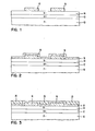
- Figs. 1 through 6 the manufacturing steps for the ultra fine dielectric isolation of one form of the invention are shown.
- the form of the invention chosen here for illustration is the fabrication of integrated bipolar circuits on silicon chips.
- Another form, such as the formation of channel stoppers in charge coupled device (CCD) arrays could have been chosen for illustration.
- the structure of Fig. 1 includes the monocrystalline silicon substrate 10 which is shown as P- conductivity for illustration purposes, an N+ layer 12 over the substrate 10 and an N- conductivity layer 14 on the layer 12.
- the layers 10, 12 and 14 could be of opposite conductivity from the conductivity types indicated.
- the layer 12 is a high conductivity region, since it will ultimately be the sub-collector of a bipolar transistor.
- This structure can be fabricated by various techniques. However, the preferred technique is to provide a P- monocrystalline silicon substrate and to diffuse an N+ blanket diffusion into the substrate by using conventional diffusion or ion implantation of an N type impurity such as arsenic, antimony or phosphorous to produce an N+ region with a surface concen- traction of between about 1 x 10 19 or 1 x 10 21 atoms/cc.
- the layer 14 is subsequently grown onto the 10, 12 structure by means of epitaxial growth.
- the N+ layer may have a typical thickness of between about 1-3 microns whereas the epitaxial layer has a thickness of from 0.5 to 10 microns, the exact thicknesses depending upon the device to be built.
- the structure could be made by various combinations of thermal diffusion, ion implantation and/or epitaxial growth which would include the formation of a varied sub- collector region where subsequent formation of bipolar devices is desired.
- buried highly doped regions or layers are not necessary and can therefore be omitted. This would be true for FET type devices.
- multiple buried highly doped regions of differenct dopant types could be formed by multiple epitaxial and diffusion processing. These structures could be needed for buried subcollector, as well as buried conductor lines.
- a first layer 16 of material such as silicon nitride or a polycrystalline silicon is deposited over the silicon body 10, 12 and 14.
- the layer 16 is then patterned by conventional lithography and etching techniques so as to form the first layer of material 16 over a first set of alternately designated device regions as shown in Fig. 1.
- the material 16 is silicon nitride, it may be deposited by any of the conventional methods for depositing silicon nitride.
- One of the common methods for depositing silicon nitride is by chemical vapor depositing using the following process conditions: SiH 4 , NH 3 and N 2 carrier gas at a temperature of about 800 °C under atmospheric or low pressure conditions as discussed in the'V. Y. Doo U.S. Patent No. 4 089 992.
- silicon nitride it is often preferred to first deposit a thin silicon dioxide layer (not shown) known as pad oxide underneath the silicon nitride layer to reduce potential stress in the silicon body.
- the material chosen for the first layer is polycrystalline silicon N or P doped polycrystalline silicon may be deposited over the entire wafer by using a mixture of silane with a suitable N or P dopant in gaseous form in a hydrogen ambient in the temperature range of 500 to 1000 °C.
- the polycrystalline silicon can be deposited without doping and then doped if desired by an ion implantation process.
- the preferred thickness of the first layer is between about 200 to 1000 nm and it is preferred to have a thickness of about 500 nm.
- the etching of the layer 16 to form the Fig. 1 structure is preferably by a reactive ion or plasma etching technique so as * to produce substantially vertical sidewall stripes of first layer 16 as shown in the Fig. 1 structure.
- a conformal coating 18 is deposited on both the substantially horizontal surfaces and substantially vertical surfaces of the first layer 16 as well as on the bare surface regions of the silicon body 10, 12 and 14.
- the bare surface regions of the silicon body includes a second set of alternately designated device regions as well as the designated isolation regions between the designated device regions.
- This conformal coating can be any one of several materials which includes . silicon dioxide, aluminum oxide and combinations of these materials. It is preferred that the coating be silicon dioxide.
- the silicon dioxide may be deposited by a chemical vapor deposition process wherein silane and oxygen gas at about 450 C is used or silicon hydrogen chloride (SiH 2 C1 2 ) and N 2 0 is used at a temperature of about 800 °C under atmospheric or low pressure conditions. Fig. 2 shows the result of this step.
- the thickness of the conformal coating 18 is chosen as the thickness of the ultimate dielectric isolation.
- the thickness of the conformal coating is between about 100 to 1000 nm and preferably 200 nm.
- a second layer 20 is now deposited over the surface of the structure.
- This material may be a plastic material such as a photoresist which may be spin coated over the structure.
- the surface is then planarized by first removing a portion of the second layer of plastic material such as by the plasma ashing technique in an oxygen ambient. The ashing process is continued until the higher regions of the conformal coating 18 are exposed as shown in the resulting Fig. 3 structure.
- a further planarization may be accomplished if desired by reactive ion etching both the second layer plastic material and the conformal coating until the first layer 16 is reached.
- the remaining conformal coating 18 between the covers of the first and second set of device regions may now be removed by a buffered hydrofluoric acid etchant wherein the conformal coating is silicon dioxide.
- the buffered hydrofluoric acid is highly selective to silicon dioxide and not to the plastic material 20 or the silicon nitride material 16.
- a reactive ion etch is now done which is anisotropic for monocrystalline silicon.
- the etching process is utilized to form the vertical sidewalls of a groove or trench 22.
- One preferred etchant is that shown in the L. E. Forget et al. U.S. Patent 4 214 946 which describes an etching gas of sulfur hexafluoride and chlorine diluted with an inert gas.
- the silicon etching utilizes the mask structure formed and shown in Fig. 4.
- the reactive ion etching process preferably continues until the etching of groove extends into the P- substrate 10 as shown in Fig. 5.
- a P+ ion implantation of for example boron is accomplished to produce regions 24 at the bottom of the grooves.
- FIG. 5 shows the resulting structure after the etching of the plastic second layer 20, first layer of silicon nitride 16 and the conformal coating layer 18. Where a thin pad oxide is used between the N- layer and layer 16, it can be removed with buffered hydrofluoric acid.
- the Fig. 5 structure is then subjected to a thermal oxidation process involving, for example, an oxygen ambient at above about 900 C for a time sufficient to thermally oxidize the grooves 22 thereby forming the dielectric isolation filled grooves 28.
- the surface of the silicon body is also thermally oxidized during this groove oxidation.
- Bipolar semiconductor devices comprising base diffusion 30, emitter diffusion 32 and collector reach through diffusion 34 are made by'conventional ion implantation or diffusion techniques as is understood by the art.
- Contact openings are made to the bipolar device region and a suitable contact metallurgy is blanket deposited over the surface, delineated by lithography and etching techniques to form the emitter contact 36, base contact 38 and collector contact 40 as shown in Fig. 6.
Abstract
Description
- The invention relates to a method for making fine deep dielectric isolation for dielectrically isolating regions of monocrystalline silicon from other regions of monocrystalline silicon, and more particularly to the formation of ultra fine widths of such isolation without the use of nonlight lithography techniques.
- In the monolithic integrated circuit technology whether for bipolar, field effect or similar devices, it is usually necessary to isolate various active and/or passive elements from one another in the integrated circuit structure. These devices have been isolated by backbiasing PN junctions, partial dielectric isolation and complete dielectric isolation. The dielectric materials used have been silicon dioxide, glass, and so forth. The preferred isolation for these active devices and circuits is some form of dielectric isolation in the highly dense integrated circuit technology. The dielectric isolation has the substantial advantage over the PN junction isolation because it allows the butting of the circuit elements against the isolation and thereby results in greater density of packing of the active and passive devices on the integrated circuit chip.
- One form of dielectric isolation involves the formation of grooves or depressions in silicon where the isolation regions are to be formed. During the groove formation, the remainder of the silicon surface is protected by a protective film which is substantially unaffected by the silicon etch used to form the grooves. The usual protective layer is a silicon nitride, silicon dioxide sandwich layer. Following the formation of the grooves by conventional chemical etching, the silicon body is subjected to a conventional oxidation step whereby the silicon in the groove area is oxidized and the silicon dioxide fills up the groove as well as oxidizing further into the silicon to form the isolation region. This process is described more fully by E. Kooi U.S. Patent No. 3 970 486, Clevenger U.S. Patent No. 3 534 234, Peltzer U.S. Patent No. 3 648 125 and I. Magdo et al.., German
patent application P 22 18 892.7. - The formation of grooves and the filling of such grooves for isolation purposes have been described by other publications such as the G. L. Kuhn, U.S. Patent Nos. 3 892 608 and 3 969 168. In these patents, chemical etching is used to form a V groove, a rounded bottom groove or a rectangular evacuated space. There is little detail as to how the groove is formed but it is clear that the groove would be limited by the nature of the chemical etching step. The process does not necessarily yield a planar surface and it requires photolithography after the formation of the grooves. D. K. Roberson U.S. Patent No. 3 956 033 describes a similar chemical etch followed by filling with polycrystalline silicon. Here again, the groove is limited by the chemical etching technique and it is unclear how the overgrowth of the polysilicon is removed. U.S. Patents K. E. Bean et al. No. 3 725 160 and W. R. Morcom et al. No. 3 979 237 also show filling of grooves. In these patents, the effect of chemical etching is more clearly brought out where it is shown that monocrystalline silicon are preferentially etched chemically to provide grooves having symmetrical sidewalls sloped at precise angles depending upon the particular face crystal to which the silicon surface is aligned.
- The Brand U.S. Patent No. 3 979 765 also describes the chemical etching to open rectangular grooves and the filling of the grooves with insulator material. However, it is difficult to understand how some of the principal steps such as etching and filling are actually effected from the description.
- The formation of rectangular grooves have been made in the Hochberg U.S. Patent No. 3 966 577 and T. Kaji et al. U.S. Patent No. 3 997 378 and S. A. Abbas, IBM TDB Vol. 20, No. 1, p. 144, June 1977 entitled "Recessed Oxide Isolation Process", and J. A. Bondur et al. U.S. Patent No. 4 104 086.
- An effective technique for accomplishing the formation of ultra fine grooves that can be then filled with dielectric material to act as dielectric isolation for highly dense integrated circuit devices has not been available. There have been other efforts to obtain narrow line widths in the range of 1 micrometer or less by extending standard photolithography techniques and avoiding the need to use the more expensive and complex techniques such as electron beam or X-ray lithography. One such technique is described by H. B. Pogge in IBM TDB, Vol. 6, November 1976, entitled "Narrow Line Widths Masking Method". This method involves the use of a porous silicon followed by oxidation of the porous silicon. The resulting structure may be used for the etching of narrow grooves into the suface of the silicon body for device isolation purposes. Another technique is described by S. A. Abbas et al., IBM TDB, Vol. 20, No. 4, September 1977, pp. 1376-1378. This TDB describes the use of polycrystalline silicon masking layers which are made into masks by first using an intermediate mask of oxidation blocking material, such as silicon nitride in the formation of the polycrystalline silicon. Line dimensions below about 2 micrometers may be obtained by this technique. M. M. Anastasio et al., "Dielectric Isolation Using Vertical Etching (DIVE)" Extended Abstracts, Vol. 78-2, No. 180, pp. 482, 483 Fall Meeting The Electrochemical Soc., October 15-20, 1978 describes the formation of narrow grooves by a somewhat complex process for dielectric isolation purposes.
- Object of the present invention is a method for making fine deep grooves that can be filled with dielectric material which can then act as dielectric isolation for highly dense integrated circuit devices.
- The object of the invention is achieved by a method comprising the following steps:
- - forming a first layer of material on a silicon body over a first set of alternately designated device regions;
- - depositing a conformal coating over said layer and on the silicon body in a second set of alternately designated device regions and the designated isolation regions in a thickness which is substantially the planned width of isolation;
- - depositing a second layer over said conformal coating;
- - planarizing the surface by removing the second layer and the conformal coating until said first layer is reached;
- - removing the portions of said conformal coating separating the covers over the first and second sets of device regions down to the silicon body in the designated isolation regions;
- - etching a groove in said silicon body using the covers as an etch mask to the desired depth of dielectric isolation in the designated isolation regions; and
- . - filling the groove with dielectric material to form deep dielectric isolation.
- In the following the method of the invention is described. Figs. 1-6 illustrate one method for forming a dielectric isolated structure of the invention.
- The method is accomplished by first forming a first layer of material on the silicon body wherein the dielectric isolation is desired. The layer material is formed over a first set of alternately designated device regions with bare silicon therebetween. A conformal coating is deposited over the first layer and on the silicon body included in a second set of alternately designated device regions and the designated isolation regions. The thickness of the coating is made to be substantially the width of the planned dielectric isolation. A second layer is then deposited over the conformal coating. The first layer and the conformal coating are composed of different materials. The topmost surface of the second layer and-the conformal coating are planarized by removing partially the second layer and conformal coating from the first layer wherein the second set of alternately designated device regions in the silicon body are covered by the conformal coating and the second layer with portions of the conformal coating separating the covers for the first and second sets of device regions. The vertical portions of the conformal coating separating the covers are then removed down to the silicon body in the designated isolation regions. These covers are then used as an etch mask for an etching of grooves in the silicon body to the desired depth of the dielectric isolation. The grooves are then filled with dielectric material to form the dielectric isolation. The preferred method of filling the grooves is by a thermal oxidation process.
- Referring now particularly to Figs. 1 through 6, the manufacturing steps for the ultra fine dielectric isolation of one form of the invention are shown. The form of the invention chosen here for illustration is the fabrication of integrated bipolar circuits on silicon chips. Another form, such as the formation of channel stoppers in charge coupled device (CCD) arrays could have been chosen for illustration. The structure of Fig. 1 includes the
monocrystalline silicon substrate 10 which is shown as P- conductivity for illustration purposes, anN+ layer 12 over thesubstrate 10 and an N-conductivity layer 14 on thelayer 12. For the purposes of the invention, either all or some of thelayers layer 12 to be a high conductivity region, since it will ultimately be the sub-collector of a bipolar transistor. This structure can be fabricated by various techniques. However, the preferred technique is to provide a P- monocrystalline silicon substrate and to diffuse an N+ blanket diffusion into the substrate by using conventional diffusion or ion implantation of an N type impurity such as arsenic, antimony or phosphorous to produce an N+ region with a surface concen- traction of between about 1 x 10¹⁹ or 1 x 10²¹ atoms/cc. Thelayer 14 is subsequently grown onto the 10, 12 structure by means of epitaxial growth. This may be done by conventional techniques such as the use of arsine in SiCl4/H2 or SiH4/H2 mixtures at growth temperatures of about 1000 °C to 1200 °C. The N+ layer may have a typical thickness of between about 1-3 microns whereas the epitaxial layer has a thickness of from 0.5 to 10 microns, the exact thicknesses depending upon the device to be built. - Alternatively the structure could be made by various combinations of thermal diffusion, ion implantation and/or epitaxial growth which would include the formation of a varied sub- collector region where subsequent formation of bipolar devices is desired.
- In certain device structures, buried highly doped regions or layers are not necessary and can therefore be omitted. This would be true for FET type devices. Alternatively, multiple buried highly doped regions of differenct dopant types could be formed by multiple epitaxial and diffusion processing. These structures could be needed for buried subcollector, as well as buried conductor lines.
- A
first layer 16 of material, such as silicon nitride or a polycrystalline silicon is deposited over thesilicon body layer 16 is then patterned by conventional lithography and etching techniques so as to form the first layer ofmaterial 16 over a first set of alternately designated device regions as shown in Fig. 1. Where thematerial 16 is silicon nitride, it may be deposited by any of the conventional methods for depositing silicon nitride. One of the common methods for depositing silicon nitride is by chemical vapor depositing using the following process conditions: SiH4, NH3 and N2 carrier gas at a temperature of about 800 °C under atmospheric or low pressure conditions as discussed in the'V. Y. Doo U.S. Patent No. 4 089 992. Where silicon nitride is used it is often preferred to first deposit a thin silicon dioxide layer (not shown) known as pad oxide underneath the silicon nitride layer to reduce potential stress in the silicon body. Where the material chosen for the first layer is polycrystalline silicon N or P doped polycrystalline silicon may be deposited over the entire wafer by using a mixture of silane with a suitable N or P dopant in gaseous form in a hydrogen ambient in the temperature range of 500 to 1000 °C. Alternately, the polycrystalline silicon can be deposited without doping and then doped if desired by an ion implantation process. The preferred thickness of the first layer is between about 200 to 1000 nm and it is preferred to have a thickness of about 500 nm. - The etching of the
layer 16 to form the Fig. 1 structure is preferably by a reactive ion or plasma etching technique so as*to produce substantially vertical sidewall stripes offirst layer 16 as shown in the Fig. 1 structure. - A
conformal coating 18 is deposited on both the substantially horizontal surfaces and substantially vertical surfaces of thefirst layer 16 as well as on the bare surface regions of thesilicon body conformal coating 18 is chosen as the thickness of the ultimate dielectric isolation. The thickness of the conformal coating is between about 100 to 1000 nm and preferably 200 nm. - A
second layer 20 is now deposited over the surface of the structure. This material may be a plastic material such as a photoresist which may be spin coated over the structure. The surface is then planarized by first removing a portion of the second layer of plastic material such as by the plasma ashing technique in an oxygen ambient. The ashing process is continued until the higher regions of theconformal coating 18 are exposed as shown in the resulting Fig. 3 structure. A further planarization may be accomplished if desired by reactive ion etching both the second layer plastic material and the conformal coating until thefirst layer 16 is reached. The remainingconformal coating 18 between the covers of the first and second set of device regions may now be removed by a buffered hydrofluoric acid etchant wherein the conformal coating is silicon dioxide. The result of this process is shown in Fig. 4. The buffered hydrofluoric acid is highly selective to silicon dioxide and not to theplastic material 20 or thesilicon nitride material 16. - A reactive ion etch is now done which is anisotropic for monocrystalline silicon. The etching process is utilized to form the vertical sidewalls of a groove or
trench 22..One preferred etchant is that shown in the L. E. Forget et al. U.S. Patent 4 214 946 which describes an etching gas of sulfur hexafluoride and chlorine diluted with an inert gas. The silicon etching utilizes the mask structure formed and shown in Fig. 4. The reactive ion etching process preferably continues until the etching of groove extends into the P-substrate 10 as shown in Fig. 5. A P+ ion implantation of for example boron is accomplished to produceregions 24 at the bottom of the grooves. ThisP+ region 24 prevents the possibility of a leakage path around the dielectric isolation from one device region to another. Fig. 5 shows the resulting structure after the etching of the plasticsecond layer 20, first layer ofsilicon nitride 16 and theconformal coating layer 18. Where a thin pad oxide is used between the N- layer andlayer 16, it can be removed with buffered hydrofluoric acid. - The Fig. 5 structure is then subjected to a thermal oxidation process involving, for example, an oxygen ambient at above about 900 C for a time sufficient to thermally oxidize the
grooves 22 thereby forming the dielectric isolation filledgrooves 28. The surface of the silicon body is also thermally oxidized during this groove oxidation. Bipolar semiconductor devices comprisingbase diffusion 30,emitter diffusion 32 and collector reach through diffusion 34 are made by'conventional ion implantation or diffusion techniques as is understood by the art. Contact openings are made to the bipolar device region and a suitable contact metallurgy is blanket deposited over the surface, delineated by lithography and etching techniques to form theemitter contact 36,base contact 38 andcollector contact 40 as shown in Fig. 6. - While the invention has been particularly shown and described with reference to the preferred embodiments thereof, it will be understood by those skilled in the art that various changes in form and detail may be made therein.without departing from the spirit and scope of the invention. For example, dielectric isolation of numerous types of devices, such as field effect transistor, charge coupled device (CCD), Schottky device, resistor, etc. can be accomplished by the present method. In fact, this invention is well suited for forming ultra fine channel stoppers in CCD arrays.
Claims (12)
Applications Claiming Priority (2)
| Application Number | Priority Date | Filing Date | Title |
|---|---|---|---|
| US06/130,882 US4274909A (en) | 1980-03-17 | 1980-03-17 | Method for forming ultra fine deep dielectric isolation |
| US130882 | 1980-03-17 |
Publications (3)
| Publication Number | Publication Date |
|---|---|
| EP0036111A2 true EP0036111A2 (en) | 1981-09-23 |
| EP0036111A3 EP0036111A3 (en) | 1986-01-02 |
| EP0036111B1 EP0036111B1 (en) | 1989-05-03 |
Family
ID=22446794
Family Applications (1)
| Application Number | Title | Priority Date | Filing Date |
|---|---|---|---|
| EP81101365A Expired EP0036111B1 (en) | 1980-03-17 | 1981-02-25 | Method for making fine deep dielectric isolation |
Country Status (4)
| Country | Link |
|---|---|
| US (1) | US4274909A (en) |
| EP (1) | EP0036111B1 (en) |
| JP (1) | JPS56137651A (en) |
| DE (1) | DE3177048D1 (en) |
Cited By (5)
| Publication number | Priority date | Publication date | Assignee | Title |
|---|---|---|---|---|
| EP0076942A2 (en) * | 1981-10-14 | 1983-04-20 | Kabushiki Kaisha Toshiba | Method of making integrated circuit device comprising dielectric isolation regions |
| EP0082256A2 (en) * | 1981-12-10 | 1983-06-29 | Kabushiki Kaisha Toshiba | Method of manufacturing a semiconductor device comprising dielectric isolation regions |
| WO1988005602A1 (en) * | 1987-01-26 | 1988-07-28 | Commissariat A L'energie Atomique | Method for producing electric insulation zones in a cmos integrated circuit |
| GB2289162A (en) * | 1994-05-04 | 1995-11-08 | Hyundai Electronics Ind | Semiconductor device with trench isolation and method for fabrication therof |
| DE102004034572A1 (en) * | 2004-07-17 | 2006-02-09 | Infineon Technologies Ag | Method for producing a structure on the surface of a substrate |
Families Citing this family (37)
| Publication number | Priority date | Publication date | Assignee | Title |
|---|---|---|---|---|
| US4394196A (en) * | 1980-07-16 | 1983-07-19 | Tokyo Shibaura Denki Kabushiki Kaisha | Method of etching, refilling and etching dielectric grooves for isolating micron size device regions |
| US4325182A (en) * | 1980-08-25 | 1982-04-20 | General Electric Company | Fast isolation diffusion |
| US4390393A (en) * | 1981-11-12 | 1983-06-28 | General Electric Company | Method of forming an isolation trench in a semiconductor substrate |
| NL8105559A (en) * | 1981-12-10 | 1983-07-01 | Philips Nv | METHOD FOR APPLYING A NARROW GROOVE IN A SUBSTRATE AREA, IN PARTICULAR A SEMICONDUCTOR SUBSTRATE AREA. |
| US4419809A (en) * | 1981-12-30 | 1983-12-13 | International Business Machines Corporation | Fabrication process of sub-micrometer channel length MOSFETs |
| JPS5935445A (en) * | 1982-08-24 | 1984-02-27 | Nippon Telegr & Teleph Corp <Ntt> | Manufacture of semiconductor device |
| US4444605A (en) * | 1982-08-27 | 1984-04-24 | Texas Instruments Incorporated | Planar field oxide for semiconductor devices |
| JPS5978542A (en) * | 1982-10-27 | 1984-05-07 | Nippon Telegr & Teleph Corp <Ntt> | Manufacture of semiconductor device |
| DE3242113A1 (en) * | 1982-11-13 | 1984-05-24 | Ibm Deutschland Gmbh, 7000 Stuttgart | METHOD FOR PRODUCING A THIN DIELECTRIC INSULATION IN A SILICON SEMICONDUCTOR BODY |
| JPS60207339A (en) * | 1984-03-30 | 1985-10-18 | Matsushita Electronics Corp | Pattern forming method |
| NL8402859A (en) * | 1984-09-18 | 1986-04-16 | Philips Nv | METHOD FOR MANUFACTURING SUBMICRON GROUPS IN E.g., SEMICONDUCTOR MATERIAL AND DEVICES OBTAINED BY THESE METHOD. |
| US4982262A (en) * | 1985-01-15 | 1991-01-01 | At&T Bell Laboratories | Inverted groove isolation technique for merging dielectrically isolated semiconductor devices |
| JPS61198780A (en) * | 1985-02-28 | 1986-09-03 | Toshiba Corp | Manufacture of semiconductor device |
| US4753901A (en) * | 1985-11-15 | 1988-06-28 | Ncr Corporation | Two mask technique for planarized trench oxide isolation of integrated devices |
| US4654119A (en) * | 1985-11-18 | 1987-03-31 | International Business Machines Corporation | Method for making submicron mask openings using sidewall and lift-off techniques |
| US4826781A (en) * | 1986-03-04 | 1989-05-02 | Seiko Epson Corporation | Semiconductor device and method of preparation |
| JPS6318673A (en) * | 1986-07-11 | 1988-01-26 | Yamaha Corp | Manufacture of semiconductor device |
| JPS6377122A (en) * | 1986-09-19 | 1988-04-07 | Matsushita Electric Ind Co Ltd | Manufacture of semiconductor device |
| JPH0727974B2 (en) * | 1988-04-26 | 1995-03-29 | 三菱電機株式会社 | Method of manufacturing semiconductor memory device |
| US5008210A (en) * | 1989-02-07 | 1991-04-16 | Hewlett-Packard Company | Process of making a bipolar transistor with a trench-isolated emitter |
| JP2870054B2 (en) * | 1989-10-25 | 1999-03-10 | ソニー株式会社 | Method for manufacturing semiconductor device |
| US5124775A (en) * | 1990-07-23 | 1992-06-23 | National Semiconductor Corporation | Semiconductor device with oxide sidewall |
| JPH0568822U (en) * | 1991-11-11 | 1993-09-17 | 株式会社日本ばし大増 | Paper case for lunch box packaging |
| US5426059A (en) * | 1994-05-26 | 1995-06-20 | Queyssac; Daniel G. | Method of making vertically stacked bipolar semiconductor structure |
| US5904539A (en) * | 1996-03-21 | 1999-05-18 | Advanced Micro Devices, Inc. | Semiconductor trench isolation process resulting in a silicon mesa having enhanced mechanical and electrical properties |
| WO1997038442A1 (en) * | 1996-04-10 | 1997-10-16 | Advanced Micro Devices, Inc. | Semiconductor trench isolation with improved planarization methodology |
| US5926713A (en) * | 1996-04-17 | 1999-07-20 | Advanced Micro Devices, Inc. | Method for achieving global planarization by forming minimum mesas in large field areas |
| US5899727A (en) * | 1996-05-02 | 1999-05-04 | Advanced Micro Devices, Inc. | Method of making a semiconductor isolation region bounded by a trench and covered with an oxide to improve planarization |
| US5929368A (en) * | 1996-12-09 | 1999-07-27 | The Ensign-Bickford Company | Hybrid electronic detonator delay circuit assembly |
| SE519975C2 (en) * | 1999-06-23 | 2003-05-06 | Ericsson Telefon Ab L M | Semiconductor structure for high voltage semiconductor components |
| EP1161769A1 (en) * | 1999-12-24 | 2001-12-12 | Koninklijke Philips Electronics N.V. | Method of manufacturing a semiconductor device comprising semiconductor elements formed in a top layer of a silicon wafer situated on a buried insulating layer |
| US20070001267A1 (en) * | 2004-11-22 | 2007-01-04 | Farrokh Ayazi | Methods of forming oxide masks with submicron openings and microstructures formed thereby |
| US20080001213A1 (en) * | 2006-06-29 | 2008-01-03 | International Business Machines Corporation | Structures and methods for manufacturing high density narrow width mosfets |
| KR100822592B1 (en) * | 2007-03-23 | 2008-04-16 | 주식회사 하이닉스반도체 | Method of forming a micro pattern in a semiconductor device |
| US8114765B2 (en) | 2008-12-31 | 2012-02-14 | Sandisk 3D Llc | Methods for increased array feature density |
| US8084347B2 (en) | 2008-12-31 | 2011-12-27 | Sandisk 3D Llc | Resist feature and removable spacer pitch doubling patterning method for pillar structures |
| US11887945B2 (en) * | 2020-09-30 | 2024-01-30 | Wolfspeed, Inc. | Semiconductor device with isolation and/or protection structures |
Citations (5)
| Publication number | Priority date | Publication date | Assignee | Title |
|---|---|---|---|---|
| DE2540352A1 (en) * | 1974-09-11 | 1976-04-08 | Hitachi Ltd | METHOD OF SELECTIVE OXYDATION |
| GB1535086A (en) * | 1976-03-22 | 1978-12-06 | Western Electric Co | Manufacture of transistors |
| EP0010624A1 (en) * | 1978-11-03 | 1980-05-14 | International Business Machines Corporation | Process for the realization of very narrow mask openings for the manufacture of semiconductor integrated circuits |
| US4211582A (en) * | 1979-06-28 | 1980-07-08 | International Business Machines Corporation | Process for making large area isolation trenches utilizing a two-step selective etching technique |
| EP0052227A1 (en) * | 1980-11-19 | 1982-05-26 | International Business Machines Corporation | Method for forming a self-aligned contact and a plasma especially applicable in performing said method |
Family Cites Families (18)
| Publication number | Priority date | Publication date | Assignee | Title |
|---|---|---|---|---|
| NL153374B (en) * | 1966-10-05 | 1977-05-16 | Philips Nv | PROCESS FOR THE MANUFACTURE OF A SEMICONDUCTOR DEVICE PROVIDED WITH AN OXIDE LAYER AND SEMI-CONDUCTOR DEVICE MANUFACTURED ACCORDING TO THE PROCEDURE. |
| US3534234A (en) * | 1966-12-15 | 1970-10-13 | Texas Instruments Inc | Modified planar process for making semiconductor devices having ultrafine mesa type geometry |
| US3725160A (en) * | 1970-12-30 | 1973-04-03 | Texas Instruments Inc | High density integrated circuits |
| US3648125A (en) * | 1971-02-02 | 1972-03-07 | Fairchild Camera Instr Co | Method of fabricating integrated circuits with oxidized isolation and the resulting structure |
| US3979237A (en) * | 1972-04-24 | 1976-09-07 | Harris Corporation | Device isolation in integrated circuits |
| US3966577A (en) * | 1973-08-27 | 1976-06-29 | Trw Inc. | Dielectrically isolated semiconductor devices |
| US3956033A (en) * | 1974-01-03 | 1976-05-11 | Motorola, Inc. | Method of fabricating an integrated semiconductor transistor structure with epitaxial contact to the buried sub-collector |
| US3892608A (en) * | 1974-02-28 | 1975-07-01 | Motorola Inc | Method for filling grooves and moats used on semiconductor devices |
| US3969168A (en) * | 1974-02-28 | 1976-07-13 | Motorola, Inc. | Method for filling grooves and moats used on semiconductor devices |
| US3979765A (en) * | 1974-03-07 | 1976-09-07 | Signetics Corporation | Silicon gate MOS device and method |
| JPS5146083A (en) * | 1974-10-18 | 1976-04-20 | Hitachi Ltd | Handotaisochino seizohoho |
| DE2547792C3 (en) * | 1974-10-25 | 1978-08-31 | Hitachi, Ltd., Tokio | Method for manufacturing a semiconductor component |
| US3920483A (en) * | 1974-11-25 | 1975-11-18 | Ibm | Method of ion implantation through a photoresist mask |
| US4037307A (en) * | 1975-03-21 | 1977-07-26 | Bell Telephone Laboratories, Incorporated | Methods for making transistor structures |
| GB1527894A (en) * | 1975-10-15 | 1978-10-11 | Mullard Ltd | Methods of manufacturing electronic devices |
| US4093503A (en) * | 1977-03-07 | 1978-06-06 | International Business Machines Corporation | Method for fabricating ultra-narrow metallic lines |
| US4104086A (en) * | 1977-08-15 | 1978-08-01 | International Business Machines Corporation | Method for forming isolated regions of silicon utilizing reactive ion etching |
| US4209350A (en) * | 1978-11-03 | 1980-06-24 | International Business Machines Corporation | Method for forming diffusions having narrow dimensions utilizing reactive ion etching |
-
1980
- 1980-03-17 US US06/130,882 patent/US4274909A/en not_active Expired - Lifetime
-
1981
- 1981-02-04 JP JP1447181A patent/JPS56137651A/en active Granted
- 1981-02-25 DE DE8181101365T patent/DE3177048D1/en not_active Expired
- 1981-02-25 EP EP81101365A patent/EP0036111B1/en not_active Expired
Patent Citations (5)
| Publication number | Priority date | Publication date | Assignee | Title |
|---|---|---|---|---|
| DE2540352A1 (en) * | 1974-09-11 | 1976-04-08 | Hitachi Ltd | METHOD OF SELECTIVE OXYDATION |
| GB1535086A (en) * | 1976-03-22 | 1978-12-06 | Western Electric Co | Manufacture of transistors |
| EP0010624A1 (en) * | 1978-11-03 | 1980-05-14 | International Business Machines Corporation | Process for the realization of very narrow mask openings for the manufacture of semiconductor integrated circuits |
| US4211582A (en) * | 1979-06-28 | 1980-07-08 | International Business Machines Corporation | Process for making large area isolation trenches utilizing a two-step selective etching technique |
| EP0052227A1 (en) * | 1980-11-19 | 1982-05-26 | International Business Machines Corporation | Method for forming a self-aligned contact and a plasma especially applicable in performing said method |
Non-Patent Citations (3)
| Title |
|---|
| IBM TECHNICAL DISCLOSURE BULLETIN, vol. 22, no. 10, March 1980, pages 4516-4517, New York, US; J.E. HITCHNER et al.: "Chromium as an RIE etch barrier" * |
| IBM TECHNICAL DISCLOSURE BULLETIN, vol. 23, no. 4, September 1980, pages 1405-1408, New York, US; C.T. HORNG et al.: "Device isolation using a narrow SiO2 trench" * |
| IEEE JOURNAL OF SOLID-STATE CIRCUITS, vol. SC-12, no. 4, August 1977, pages 363-367, New York, US; H.H. HOSACK et al.: "Submicron patterning of surfaces" * |
Cited By (13)
| Publication number | Priority date | Publication date | Assignee | Title |
|---|---|---|---|---|
| EP0076942A2 (en) * | 1981-10-14 | 1983-04-20 | Kabushiki Kaisha Toshiba | Method of making integrated circuit device comprising dielectric isolation regions |
| EP0076942A3 (en) * | 1981-10-14 | 1986-04-16 | Kabushiki Kaisha Toshiba | Method of making integrated circuit device comprising dielectric isolation regions |
| EP0082256A2 (en) * | 1981-12-10 | 1983-06-29 | Kabushiki Kaisha Toshiba | Method of manufacturing a semiconductor device comprising dielectric isolation regions |
| EP0082256A3 (en) * | 1981-12-10 | 1986-05-07 | Kabushiki Kaisha Toshiba | Method of manufacturing a semiconductor device comprising dielectric isolation regions |
| US4882291A (en) * | 1987-01-26 | 1989-11-21 | Commissiriat A L'energie Atomique | Process for the production of electrical isolation zones in a CMOS integrated circuit |
| FR2610141A1 (en) * | 1987-01-26 | 1988-07-29 | Commissariat Energie Atomique | CMOS INTEGRATED CIRCUIT AND METHOD FOR MANUFACTURING ELECTRICAL ISOLATION AREAS IN THIS CIRCUIT |
| WO1988005602A1 (en) * | 1987-01-26 | 1988-07-28 | Commissariat A L'energie Atomique | Method for producing electric insulation zones in a cmos integrated circuit |
| GB2289162A (en) * | 1994-05-04 | 1995-11-08 | Hyundai Electronics Ind | Semiconductor device with trench isolation and method for fabrication therof |
| GB2289162B (en) * | 1994-05-04 | 1998-07-22 | Hyundai Electronics Ind | Method for fabricating a semiconductor device |
| DE102004034572A1 (en) * | 2004-07-17 | 2006-02-09 | Infineon Technologies Ag | Method for producing a structure on the surface of a substrate |
| DE102004034572B4 (en) * | 2004-07-17 | 2008-02-28 | Infineon Technologies Ag | Method for producing a structure on the surface of a substrate |
| US7368385B2 (en) | 2004-07-17 | 2008-05-06 | Infineon Technologies Ag | Method for producing a structure on the surface of a substrate |
| US8003538B2 (en) | 2004-07-17 | 2011-08-23 | Qimonda Ag | Method for producing a structure on the surface of a substrate |
Also Published As
| Publication number | Publication date |
|---|---|
| EP0036111B1 (en) | 1989-05-03 |
| JPS56137651A (en) | 1981-10-27 |
| EP0036111A3 (en) | 1986-01-02 |
| DE3177048D1 (en) | 1989-06-08 |
| US4274909A (en) | 1981-06-23 |
| JPS6145382B2 (en) | 1986-10-07 |
Similar Documents
| Publication | Publication Date | Title |
|---|---|---|
| EP0036111B1 (en) | Method for making fine deep dielectric isolation | |
| US4502913A (en) | Total dielectric isolation for integrated circuits | |
| US4771328A (en) | Semiconductor device and process | |
| US4307180A (en) | Process of forming recessed dielectric regions in a monocrystalline silicon substrate | |
| US4104086A (en) | Method for forming isolated regions of silicon utilizing reactive ion etching | |
| US4256514A (en) | Method for forming a narrow dimensioned region on a body | |
| EP0072966B1 (en) | Integrated circuit structure and method for forming a recessed isolation structure for integrated circuits | |
| US4519128A (en) | Method of making a trench isolated device | |
| CA1120609A (en) | Method for forming a narrow dimensioned mask opening on a silicon body | |
| EP0073370B1 (en) | Integrated circuit structure and method for forming a recessed isolation structure for integrated circuits | |
| EP0083089B1 (en) | Process for forming self-aligned metallization patterns for semiconductor devices | |
| US4333794A (en) | Omission of thick Si3 N4 layers in ISA schemes | |
| JPH0344419B2 (en) | ||
| US4661832A (en) | Total dielectric isolation for integrated circuits | |
| EP0193116B1 (en) | Method of manufacturing a semiconductor device having a trench | |
| US4876214A (en) | Method for fabricating an isolation region in a semiconductor substrate | |
| US4389294A (en) | Method for avoiding residue on a vertical walled mesa | |
| US4824794A (en) | Method for fabricating a bipolar transistor having self aligned base and emitter | |
| US4026736A (en) | Integrated semiconductor structure with combined dielectric and PN junction isolation including fabrication method therefor | |
| US4696095A (en) | Process for isolation using self-aligned diffusion process | |
| US4056414A (en) | Process for producing an improved dielectrically-isolated silicon crystal utilizing adjacent areas of different insulators | |
| EP0146760B1 (en) | One mask technique for substrate contacting in integrated circuits | |
| US4546537A (en) | Method for producing a semiconductor device utilizing V-groove etching and thermal oxidation | |
| EP0137195B1 (en) | Dielectric isolated circuit and method of making | |
| JPS58200554A (en) | Manufacture of semiconductor device |
Legal Events
| Date | Code | Title | Description |
|---|---|---|---|
| PUAI | Public reference made under article 153(3) epc to a published international application that has entered the european phase |
Free format text: ORIGINAL CODE: 0009012 |
|
| AK | Designated contracting states |
Designated state(s): DE FR GB IT |
|
| 17P | Request for examination filed |
Effective date: 19811020 |
|
| PUAL | Search report despatched |
Free format text: ORIGINAL CODE: 0009013 |
|
| AK | Designated contracting states |
Designated state(s): DE FR GB IT |
|
| 17Q | First examination report despatched |
Effective date: 19870626 |
|
| GRAA | (expected) grant |
Free format text: ORIGINAL CODE: 0009210 |
|
| AK | Designated contracting states |
Kind code of ref document: B1 Designated state(s): DE FR GB IT |
|
| PG25 | Lapsed in a contracting state [announced via postgrant information from national office to epo] |
Ref country code: IT Free format text: LAPSE BECAUSE OF FAILURE TO SUBMIT A TRANSLATION OF THE DESCRIPTION OR TO PAY THE FEE WITHIN THE PRESCRIBED TIME-LIMIT;WARNING: LAPSES OF ITALIAN PATENTS WITH EFFECTIVE DATE BEFORE 2007 MAY HAVE OCCURRED AT ANY TIME BEFORE 2007. THE CORRECT EFFECTIVE DATE MAY BE DIFFERENT FROM THE ONE RECORDED. Effective date: 19890503 |
|
| REF | Corresponds to: |
Ref document number: 3177048 Country of ref document: DE Date of ref document: 19890608 |
|
| ET | Fr: translation filed | ||
| PLBE | No opposition filed within time limit |
Free format text: ORIGINAL CODE: 0009261 |
|
| STAA | Information on the status of an ep patent application or granted ep patent |
Free format text: STATUS: NO OPPOSITION FILED WITHIN TIME LIMIT |
|
| 26N | No opposition filed | ||
| PGFP | Annual fee paid to national office [announced via postgrant information from national office to epo] |
Ref country code: GB Payment date: 19910118 Year of fee payment: 11 |
|
| PGFP | Annual fee paid to national office [announced via postgrant information from national office to epo] |
Ref country code: DE Payment date: 19910204 Year of fee payment: 11 |
|
| PGFP | Annual fee paid to national office [announced via postgrant information from national office to epo] |
Ref country code: FR Payment date: 19920124 Year of fee payment: 12 |
|
| PG25 | Lapsed in a contracting state [announced via postgrant information from national office to epo] |
Ref country code: GB Effective date: 19920225 |
|
| GBPC | Gb: european patent ceased through non-payment of renewal fee | ||
| PG25 | Lapsed in a contracting state [announced via postgrant information from national office to epo] |
Ref country code: DE Effective date: 19921103 |
|
| PG25 | Lapsed in a contracting state [announced via postgrant information from national office to epo] |
Ref country code: FR Effective date: 19931029 |
|
| REG | Reference to a national code |
Ref country code: FR Ref legal event code: ST |