EP0041642B2 - Integrated laminating process - Google Patents
Integrated laminating process Download PDFInfo
- Publication number
- EP0041642B2 EP0041642B2 EP81104013A EP81104013A EP0041642B2 EP 0041642 B2 EP0041642 B2 EP 0041642B2 EP 81104013 A EP81104013 A EP 81104013A EP 81104013 A EP81104013 A EP 81104013A EP 0041642 B2 EP0041642 B2 EP 0041642B2
- Authority
- EP
- European Patent Office
- Prior art keywords
- layer
- substrate
- laminated
- photosensitive
- alkyl
- Prior art date
- Legal status (The legal status is an assumption and is not a legal conclusion. Google has not performed a legal analysis and makes no representation as to the accuracy of the status listed.)
- Expired
Links
Images
Classifications
-
- B—PERFORMING OPERATIONS; TRANSPORTING
- B32—LAYERED PRODUCTS
- B32B—LAYERED PRODUCTS, i.e. PRODUCTS BUILT-UP OF STRATA OF FLAT OR NON-FLAT, e.g. CELLULAR OR HONEYCOMB, FORM
- B32B37/00—Methods or apparatus for laminating, e.g. by curing or by ultrasonic bonding
- B32B37/14—Methods or apparatus for laminating, e.g. by curing or by ultrasonic bonding characterised by the properties of the layers
- B32B37/16—Methods or apparatus for laminating, e.g. by curing or by ultrasonic bonding characterised by the properties of the layers with all layers existing as coherent layers before laminating
- B32B37/22—Methods or apparatus for laminating, e.g. by curing or by ultrasonic bonding characterised by the properties of the layers with all layers existing as coherent layers before laminating involving the assembly of both discrete and continuous layers
- B32B37/223—One or more of the layers being plastic
- B32B37/226—Laminating sheets, panels or inserts between two continuous plastic layers
-
- B—PERFORMING OPERATIONS; TRANSPORTING
- B26—HAND CUTTING TOOLS; CUTTING; SEVERING
- B26D—CUTTING; DETAILS COMMON TO MACHINES FOR PERFORATING, PUNCHING, CUTTING-OUT, STAMPING-OUT OR SEVERING
- B26D7/00—Details of apparatus for cutting, cutting-out, stamping-out, punching, perforating, or severing by means other than cutting
- B26D7/18—Means for removing cut-out material or waste
-
- B—PERFORMING OPERATIONS; TRANSPORTING
- B29—WORKING OF PLASTICS; WORKING OF SUBSTANCES IN A PLASTIC STATE IN GENERAL
- B29C—SHAPING OR JOINING OF PLASTICS; SHAPING OF MATERIAL IN A PLASTIC STATE, NOT OTHERWISE PROVIDED FOR; AFTER-TREATMENT OF THE SHAPED PRODUCTS, e.g. REPAIRING
- B29C63/00—Lining or sheathing, i.e. applying preformed layers or sheathings of plastics; Apparatus therefor
- B29C63/0004—Component parts, details or accessories; Auxiliary operations
- B29C63/0013—Removing old coatings
-
- B—PERFORMING OPERATIONS; TRANSPORTING
- B32—LAYERED PRODUCTS
- B32B—LAYERED PRODUCTS, i.e. PRODUCTS BUILT-UP OF STRATA OF FLAT OR NON-FLAT, e.g. CELLULAR OR HONEYCOMB, FORM
- B32B39/00—Layout of apparatus or plants, e.g. modular laminating systems
-
- G—PHYSICS
- G03—PHOTOGRAPHY; CINEMATOGRAPHY; ANALOGOUS TECHNIQUES USING WAVES OTHER THAN OPTICAL WAVES; ELECTROGRAPHY; HOLOGRAPHY
- G03F—PHOTOMECHANICAL PRODUCTION OF TEXTURED OR PATTERNED SURFACES, e.g. FOR PRINTING, FOR PROCESSING OF SEMICONDUCTOR DEVICES; MATERIALS THEREFOR; ORIGINALS THEREFOR; APPARATUS SPECIALLY ADAPTED THEREFOR
- G03F7/00—Photomechanical, e.g. photolithographic, production of textured or patterned surfaces, e.g. printing surfaces; Materials therefor, e.g. comprising photoresists; Apparatus specially adapted therefor
- G03F7/16—Coating processes; Apparatus therefor
- G03F7/161—Coating processes; Apparatus therefor using a previously coated surface, e.g. by stamping or by transfer lamination
-
- B—PERFORMING OPERATIONS; TRANSPORTING
- B29—WORKING OF PLASTICS; WORKING OF SUBSTANCES IN A PLASTIC STATE IN GENERAL
- B29L—INDEXING SCHEME ASSOCIATED WITH SUBCLASS B29C, RELATING TO PARTICULAR ARTICLES
- B29L2031/00—Other particular articles
- B29L2031/34—Electrical apparatus, e.g. sparking plugs or parts thereof
- B29L2031/3425—Printed circuits
-
- B—PERFORMING OPERATIONS; TRANSPORTING
- B32—LAYERED PRODUCTS
- B32B—LAYERED PRODUCTS, i.e. PRODUCTS BUILT-UP OF STRATA OF FLAT OR NON-FLAT, e.g. CELLULAR OR HONEYCOMB, FORM
- B32B38/00—Ancillary operations in connection with laminating processes
- B32B38/16—Drying; Softening; Cleaning
- B32B38/162—Cleaning
-
- H—ELECTRICITY
- H05—ELECTRIC TECHNIQUES NOT OTHERWISE PROVIDED FOR
- H05K—PRINTED CIRCUITS; CASINGS OR CONSTRUCTIONAL DETAILS OF ELECTRIC APPARATUS; MANUFACTURE OF ASSEMBLAGES OF ELECTRICAL COMPONENTS
- H05K3/00—Apparatus or processes for manufacturing printed circuits
- H05K3/0073—Masks not provided for in groups H05K3/02 - H05K3/46, e.g. for photomechanical production of patterned surfaces
- H05K3/0079—Masks not provided for in groups H05K3/02 - H05K3/46, e.g. for photomechanical production of patterned surfaces characterised by the method of application or removal of the mask
-
- Y—GENERAL TAGGING OF NEW TECHNOLOGICAL DEVELOPMENTS; GENERAL TAGGING OF CROSS-SECTIONAL TECHNOLOGIES SPANNING OVER SEVERAL SECTIONS OF THE IPC; TECHNICAL SUBJECTS COVERED BY FORMER USPC CROSS-REFERENCE ART COLLECTIONS [XRACs] AND DIGESTS
- Y10—TECHNICAL SUBJECTS COVERED BY FORMER USPC
- Y10T—TECHNICAL SUBJECTS COVERED BY FORMER US CLASSIFICATION
- Y10T156/00—Adhesive bonding and miscellaneous chemical manufacture
- Y10T156/10—Methods of surface bonding and/or assembly therefor
- Y10T156/1052—Methods of surface bonding and/or assembly therefor with cutting, punching, tearing or severing
- Y10T156/1084—Methods of surface bonding and/or assembly therefor with cutting, punching, tearing or severing of continuous or running length bonded web
- Y10T156/1085—One web only
-
- Y—GENERAL TAGGING OF NEW TECHNOLOGICAL DEVELOPMENTS; GENERAL TAGGING OF CROSS-SECTIONAL TECHNOLOGIES SPANNING OVER SEVERAL SECTIONS OF THE IPC; TECHNICAL SUBJECTS COVERED BY FORMER USPC CROSS-REFERENCE ART COLLECTIONS [XRACs] AND DIGESTS
- Y10—TECHNICAL SUBJECTS COVERED BY FORMER USPC
- Y10T—TECHNICAL SUBJECTS COVERED BY FORMER US CLASSIFICATION
- Y10T156/00—Adhesive bonding and miscellaneous chemical manufacture
- Y10T156/17—Surface bonding means and/or assemblymeans with work feeding or handling means
- Y10T156/1702—For plural parts or plural areas of single part
- Y10T156/1705—Lamina transferred to base from adhered flexible web or sheet type carrier
- Y10T156/1707—Discrete spaced laminae on adhered carrier
- Y10T156/171—Means serially presenting discrete base articles or separate portions of a single article
Definitions
- the invention relates to an integrated process for laminating a continuous layer of photosensitive composition to a surface of each member of a series of substrate elements and trimming the layer from at least one of the transverse edges of the laminated substrate elements.
- U.S. Patent 3,469,982 discloses a photoresist process comprising applying a photopolymerizable layer supported on a support film to a surface, followed by imagewise exposure of the layer, stripping away the support film, and washing away the unexposed area of the layer to leave a resist image protecting the aforesaid surface from such treatments as etching or plating.
- the patent discloses solution coating of a photopolymerizable composition onto the support film, followed by drying and then lamination of the resultant dry coating to a surface such as copper-clad printed circuit board (Example V) to carry out the photoresist process.
- a surface such as copper-clad printed circuit board (Example V) to carry out the photoresist process.
- the dried photopolymerizable coating which must remain adhered to the support during storage and shipment, has always been supplied sandwiched between the support film and a cover sheet, such as disclosed in Example I of the patent. This has enabled the sandwich to be rolled up upon itself by the photoresist manufacturer and be supplied to the user, e.g. printed circuit manufacturer, as a compact, easy to handle roll.
- the cover sheet permitted the roll to be unrolled by the user.
- the equipment used to practise the photoresist process has consisted in general of separate pieces of equipment, such as a cleaner, scrubber for cleaning the copper-clad circuit boards, oven for preheating the boards, roll laminator applying heat to the photoresist and board as it laminates them together, and exposure (actinic radiation) station, and solvent development apparatus.
- a cleaner, scrubber for cleaning the copper-clad circuit boards
- oven for preheating the boards
- roll laminator applying heat to the photoresist and board as it laminates them together
- exposure (actinic radiation) station and solvent development apparatus.
- U.S. Patent 3,547,730 discloses a process and apparatus for automating the photoresist process, involving a device for sequential feeding of shaped articles such as circuit boards and a laminator for receiving the boards and laminating a photosensitive layer thereto.
- Sequentially laminated boards become tied together by a web of support film and the photosensitive layer extending between boards as shown in Fig. 2, and the layer of the top and bottom web become laminated together to form a "hinge" (col. 5, lines 35-39).
- the support film is stripped away by rolls 12 and 13. This stripping away provides a forwarding motion to the circuit board to bring it into abutting relationship with the preceding board to force it into the exposure unit.
- U.S. Patent 3,547,730 also discloses the cleaning of a circuit board between a feed station and lamination station, the preheating of the board and/or photosensitive layer between their respective feeds and the lamination station, and rolls 10 for stripping away the cover sheet prior to lamination.
- U.S. Patent 4,025,380 discloses the sequential feeding of circuit boards onto a conveyor which passes them through an infrared preheater and then past sensor switches which control the operation of laminating rolls and cutting devices which cut a photosensitive layer to the desired length prior to lamination and then laminate the cut sheet (layer) to the circuit board.
- the patent also discloses rolls 63 for stripping off of the cover film prior to the lamination.
- U.S. Patent 3,629,036 discloses that the elevated temperature required for laminating a photoresist to a substrate introduces disadvantages of limiting the types of photoresist and substrate materials that can be used and produces inferior bonding to the substrate.
- the patent purports to solve these problems by room temperature lamination after first applying a solution of dissolved resist to the substrate and then doing the lamination.
- the patent provides for a release layer between the photoresist layer and its support film to enable the film to be stripped away from the photoresist layer after lamination.
- U.S. Patent 3,794,546 discloses the use of an adhesive web to adhere to a support film of a photohardenable element so as to delaminate the support film from at least the unhardened area of an image wise exposed photohardenable layer laminated to a receptor sheet.
- U.S. Patent 4,075,051 discloses a process for self trimming of a photoresist layer laminated to a substrate, i.e. the portion of the layer extending past the edges of the substrate without any cutting step. This is accomplished by applying a liquid weakening agent at leastto the aforesaid portion of the layer, but possibly to the entire layer by pre-wetting of the substrate with the agent, and then peeling away either the cover sheet (support film) or an auxiliary permeable sheet which has a greater adhesion to the layer than the cohesive strength (as a result of the weakening agent) of the layer.
- the weakening agent is either a solvent for the photoresist or is a softening agent for it.
- the patent discloses the use of a conventional roll type laminator and pressure and heat for adhering the photoresist layer to the substrate.
- the invention is directed to an integrated process for laminating a continuous layer of photosensitive composition to a surface of each member of a series of substrate elements and trimming the layer from at least one of the transverse edges of the laminated substrate elements comprising the sequential steps of:
- the support film is removed from the layer as it emerges from the nip of the laminating rolls by bending the film back along the longitudinal axis of the advancing layer at an obtuse angle, the radius of the bend being sufficiently small that the breaking strength of the layer on the leading edge of the substrate element is exceeded.
- the invention may be used advantageously in the lamination of a broad spectrum of thermoplastic layers.
- the invention is particularly useful for the lamination of photosensitive resist elements to substrates which are to be used for making printed circuit boards.
- the invention is also useful for lamination of photosensitive layers to substrates in the preparation of lithographic printing plates.
- photosensitive film resists of various types may be used.
- negative-working resists are photopolymerizable films of the type disclosed in U.S. Patent 3,469,982 and the photocrosslinkable elements of the type disclosed in U.S. Patent 3,526,504.
- Positive-working, resist elements may be of the photosolubilizable type, e.g., such as the o-quinone diazide elements of U.S. Patent 3,837,860, or of the photodesensitizable type, e.g., such as the bisdiazonium salts of U.S. Patent 3,778,270 or the nitroaromatic composition of U.K. Patent 1,547,548.
- the photosensitive layer used in the process is preferably aqueous alkali processible in the sense that it is soluble and thereby developable in aqueous alkali solution, e.g., 1 wt% Na 2 C0 3 at 29.4°C for 90 seconds at a spray pressure of 1.38 kg/cm 2 .
- An element containing an image-yielding, non-blocking photopolymerizable stratum on a strippable support is preferably used such as the one described in European Patent Application No. 81 103 965.0.
- the remaining surface of the supported, photopolymerizable stratum may be protected by a removable cover sheet or when the element is stored in roll form, the stratum surface may be protected by the contiguous reverse surface of the support.
- the photosensitive composition is present in a dry coating thickness of about 0.0003 inch (-0.0008 cm) to about 0.01 inch (-0.025 cm) or more.
- a suitable strippable support which preferably has a high degree of dimensional stability to temperature changes, may be chosen from a wide variety of films composed of high polymers, e.g. polyamides, polyolefins, polyesters, vinyl polymers, and cellulose esters, and may have a thickness of from 0.00025 inch (-0.0006 cm) to 0.008 inch (-0.02 cm) or more.
- a particularly suitable support is a transparent polyethylene terephthalate film having a thickness of about 0.001 inch (-0.0025 cm).
- the adhesion (A,) of the unexposed photosensitive layer to the polymeric support exceeds the breaking strength (B) of the unsupported photosensitive layer.
- the adhesion (A 2 ) of the unexposed photosensitive layer to the substrate must exceed the breaking strength (B) of the unsupported photosensitive layer.
- the adhesion (A 2 ) of the photolayer to the substrate must also exceed its adhesion (A,) to the polymeric support. Expressed methamatically, A 2 >A,>B.
- the photosensitive layer is also preferably compounded to be relatively hard and nonblocking, i.e., it will not stick to itself or the film support with a greater adhesive strength than the cohesive strength of the layer.
- a cover sheet is not necessary to prevent the layer from sticking to the support film while in the rolled-up condition for the photosensitive element. This provides a saving in material costs and eliminates the need for cover sheet stripping and disposal of the stripped cover sheet.
- additional protection against blocking can optionally be provided if the reverse side of the strippable support has applied thereto a thin release layer of a material, such as wax or silicone, to prevent blocking with the photopolymerizable stratum.
- adhesion to the coated photopolymerizable layer may be preferentially increased by flame treating or electrical discharge treating the support surface to be coated.
- Suitable removable, protective cover sheets when used may be chosen from the same group of high polymer films described above and may have the same wide range of thicknesses.
- a cover sheet of 0.001 inch (-0.0025 cm) thick polyethylene is especially suitable. Supports and cover sheets as described above provide good protection to the photopolymerizable resist layer.
- the photohardenable layer is prepared from polymeric components (binders), monomeric components, initiators and inhibitors.
- Suitable binders which can be used as the sole binder or in combination with others include the following: polyacrylate and alpha-alkyl polyacrylate esters, e.g., polymethyl methacrylate and polyethyl methacrylate; polyvinyl esters, e.g., polyvinyl esters, e.g.
- polyvinyl acetate polyvinyl acetate/acrylate, polyvinyl acetate/methacrylate and hydrolyzed polyvinyl acetate; ethylene/vinyl acetate copolymers; polystyrene polymers and copolymers, e.g., with maleic anhydride and esters; vinylidene chloride copolymers, e.g., vinylidene chloride/acrylonitrile; vinylidene chloride/methacrylate and vinylidene chloride/vinyl acetate copolymers, polyvinyl chloride and copolymers, e.g., polyvinyl chloride/acetate; saturated and unsaturated polyurethanes; synthetic rubbers, e.g.
- butadiene/acrylonitrile acrylonitrile/buta- diene/styrene, methacrylate/acrylonitrile/butadiene/styrene copolymers, 2-chlorobutadiene-1,3 polymers, chlorinated rubber and styrene/butadiene/styrene, styrene/isoprene/styrene block copolymers; high molecular weight polyethylene oxides of polyglycols having average molecular weights from about 4,000 to 1,000,000; epoxides, e.g.
- copolyesters e.g., those prepared from the reaction product of a polymethylene glycol of the formula HO(CH 2 ) n OH, where n is a whole number 2 to 10 inclusive, and (1) hexahydroterephthalic, sebacic and terephthalic acids, (2) terephthalic, isophthalic and sebacic acids, (3) terephthalic and sebacic acids, (4) terephthalic and isophthalic acids, and (5) mixtures of copolyesters prepared from said glycols and (i) terephthalic isophthalic and sebacid acids and (ii) terephthalic, isophthalic sebacic and adipic acids; nylons or polyamides, e.g., N-methoxymethyl polyhexamethylene adipamide; cellulose esters, e.g., cellulose acetate, cellulose acetate succinate and
- the binder should contain sufficient acidic or other groups to render the composition processible in aqueous developer as described hereinbefore.
- Useful aqueous-processible binders include those disclosed in U.S. Patent 3,458,311 and in U.K. 1,507,704.
- Useful amphoteric polymers include interpolymers derived from N-alkylacrylamides or methacrylamides, acidic film-forming comonomer and an alkyl or hydroalkyl acrylate such as those disclosed in U.S. Patent 3,927,199 which is incorporated herein by reference.
- the photosensitive layer be relatively harder than those which generally have been available before now. Greater hardness of the layer provides greater dimensional stability and thus there is less requirement for support by the support film.
- Suitable monomers which can be used as the sole monomer or in combination with others include the following: t-butyl acrylate, 1,5-pentanediol diacrylate, N,N-diethylaminoethyl acrylate, ethylene glycol diacrylate, 1,4-butanediol diacrylate, diethylene glycol diacrylate, hexamethylene glycol diacrylate, 1,3-propanediol diacrylate, decamethylene glycol diacrylate, decamethylene glycol dimethacrylate, 1,4-cyclohexane diol diacrylate, 2,2-dimethylolpropane diacrylate, glycerol diacrylate, tripropylene glycol diacrylate, glycerol triacrylate, trimethylolpropane triacrylate, pentaerythritol triacrylate, polyoxyethylated trimethylolpropane triacrylate and trimethacrylate and similar compounds as disclosed in U.S.
- Patent 3,380,831 2,2-di(p-hydroxyphenyl)propane diacrylate, pentaerythritol tetraacrylate, 2,2-di-(p-hydroxyphenyl)propane dimethacrylate, triethylene glycol diacrylate, polyoxyethyl-2,2-di-(p-hydroxyphenylpropane dimethacrylate, di-(3-methacryloxy-2-hydroxypropyl) ether of bisphenol-A, di(2-methacryloxyethyl) ether of bisphenol-A, di(3-acryloxy-2-hydroxypropyl) ether of bisphenol-A, di(2-acryloxyethyl) ether of bisphenol-A, di(3-methacryloxy-2-hydroxypropyl) ether of tetrachloro-bisphenol-A, di(2-methacryloxyethyl)ether of tetrachloro-bisphenol-A, di-(3-methacryloxy-2-hydroxypropy
- the photohardenable layer can also contain at least one of the following free radical-initiated, chain-propagating, addition- polymerizable, ethylenically unsaturated compounds having a molecular weight of at least 300.
- Preferred monomers of this type are an alkylene or a polyalkylene glycol diacrylate prepared from an alkylene glycol of 2 to 15 carbons or a polyalkylene ether glycol of 1 to 10 ether linkages, and those disclosed in U.S. Patent 2,927,022, e.g., those having a plurality of addition polymerizable ethylenic linkages particularly when present as terminal linkages.
- linkages are conjugated with a double bonded carbon, including carbon double bonded to carbon and to such heteroatoms as nitrogen, oxygen and sulfur.
- ethylenically unsaturated groups, especially the vinylidene groups are conjugated with ester or amide structures.
- Preferred free radical-generating addition-polymerization initiators activatable by actinic light and thermally inactive at and below 185°C include the substituted or unsubstituted polynuclear quinones which are compounds having two intracyclic carbon atoms in a conjugated carbocyclic ring system e.g., 9, 10- anthraquinone, 1-chloroanthraquinone, 2-chloroanthraquinone, 2-methylanthraquinone, 2-ethylanthraquinone, 2-tert-butylanthraquinone, octamethylanthraquinone, 1,4-naphthoquinone, 9,10-phenanthrenequinone, 1,2-benzanthraquinone, 2,3-benzanthraquinone, 2-methyl-1,4-naphthoquinone, 2,3-dichloronaphthoquinone, 1,4-dimethyi
- photoinitiators which are also useful, even those some may be thermally active at temperatures as low as 85°C, are described in U.S. Patent 2,760,863 and include vicinal ketaldonyl alcohols, such as benzoin, pivaloin, acyloin ethers, e.g., benzoin methyl and ethyl ethers; a-hydrocarbon-substituted aromatic acyloins, including a-methylbenzoin, a-allylbenzoin and a-phenylbenzoin. Photoreducible dyes and reducing agents disclosed in U.S.
- Patents 2,850,445; 2,875,047; 3,097,096; 3,074,974; 3,097,097; and 3,145,104 as well as dyes of the phenazine, oxazine, and quinone classes; Michler's ketone, benzophenone, 2,4,5-triphenyl-imidazolyl dimers with hydrogen donors, and mixtures thereof as described in U.S. Patents: 3,427,161; 3,479,185; and 3,549,367 can be used as initiators. Also useful with photoinitiators and photoinhibitors are sensitizers disclosed in U.S. Patent 4,162,162.
- Thermal polymerization inhibitors that can be used in photopolymerizable compositions are: p-methoxyphenol, hydroquinone, and alkyl and aryl-substituted hydroquinones and quinones, tert-butyl catechol, pyrogallol, copper resinate, naphthylamines, beta-naphthol, cuprous chloride, 2,6-di-tert-butyl-p-cresol, phenothiazine, pyridine, nitrobenzene and dinitrobenzene, p-toluquinone and chloranil. Also useful for thermal polymerization inhibitors are the nitroso compositions disclosed in U.S. 4,168,982.
- Various dyes and pigments may be added to increase the visibility of the resist image. Any colorant used, however, should preferably be transparent to the actinic radiation used.
- suitable substrates for the process of the invention involving printed circuit formation are those which have mechanical strength, chemical resistance and good dielectric properties.
- board materials for printed circuits are thermosetting or thermoplastic resins usually combined with a reinforcing agent.
- Thermosetting resins with reinforcing fillers are ordinarily used for rigid boards, whereas thermoplastic resin without reinforcements are usually used for flexible circuit boards. Ceramic and dielectric coated metals are also useful.
- Typical board construction involves combinations such as phenolic or epoxy resins on paper or a paper-glass composite, as well as polyester, epoxy, polyimide, polytetrafluorethylene, or polystyrene on glass. In most instances, the board is clad with a thin layer of electroconductive metal of which copper is by far the most common.
- Suitable substrates for the process of the invention involving preparation of lithographic printing plates are those which have mechanical strength and surfaces which differ in hydrophilicity or oleophilicity from the surfaces of the images photosensitive areas laminated thereto.
- Such substrates are disclosed in U.S. Patent 4,072,528. While numerous substrates are satisfactory for this purpose thin anodized aluminum plates such as disclosed in U.S. Patent 3,458,311 are particularly useful.
- the adhesion of the unexpected photosensitive layer to substrates such as copper or aluminum must be greater than its breaking strength (B) and its adhesion to the support (A 1 ).
- a high value for A 2 is also needed for many of the applications of this invention where the photosensitive layer must remain adhered to the substrate during exposure to severe chemical or mechanical conditions.
- the printed circuit substrates used be clean and free of any extraneous materials to insure that these materials do not interfere with wetting and bonding of the surface. For this reason, it will frequently be desired to clean printed circuit substrates prior to lamination by one or more of the several cleaning processes which are well-known in the field of printed circuit board manufacture.
- the particular type of cleaning depends upon the type of contamination - organic, particulate or metallic. Such methods include degreasing with solvents and solvent emulsions, mechanical scrubbing, alkaline soaks, acidification and the like, followed by rinsing and drying.
- Suitable cleanliness can be very easily determined by the Uniform Water Film test in which the substrate is dipped into water, removed from the water and then the board surface is observed. If a uniform film of water is observed, the board is adequately clean but if a discontinuous streaked film or large droplets are formed, the board is not sufficiently clean to be used in the process of the invention.
- thermoplastic layer is laminated to the substrate by means of nip rolls.
- the photosensitive layer of the element it is necessary to laminate the photosensitive layer of the element to the substrate board in such manner that the layer is firmly adhered thereto without occlusions and other phase discontinuities such as entrapped air or liquids. Cleaned surfaces tend to deteriorate rapidly immediately after cleaning, e.g., by oxidation or dust. Therefore in a preferred method of practicing the invention, the surface of the substrate, just prior to lamination, is treated to improve adhesion between the photosensitive layer and the substrate by the sequential steps of:
- the inert liquid is a nonsolvent with respect to the thermoplastic layer.
- the thin layer of inert liquid is applied to the substrate surface by contacting the surface at a temperature below the condensation point of the liquid with a vapor or gaseous dispersion of the liquid.
- the inert liquid used to form the film can also be applied in other ways, for example, by brushing, wicking, atomizing spray or by rolling it on using perforated or porous rolls.
- the thin liquid layer should cover at least 30 percent of the substrate surface on which the polymer is to be laminated and preferably at least 80 percent. Essentially complete coverage is still further preferred.
- the liquid layer should be sufficiently thin for adhesion to the substrate to occur almost instantaneously.
- the liquid should not flood the surface of the substrate such as described in U.S. Patent 4,069,076. Excess liquid interferes with instant adhesion and furthermore fills the interconnective holes which are normally present in a printed circuit substrate and thereby acts as a contaminant in subsequent processing operations.
- the thin liquid layer be as thin as is practicable to displace air at the interface and promote adhesion of the photosensitive layer. While the particular layer thickness will vary somewhat, depending upon the nature of the liquid and the conditions of application, it is generally preferred that it be much thinner than in the prior art proccesses, e.g., from 1-50 pm, the average layer thickness being about 30 ⁇ ..lm or a preferred range from about 10 to about 50 pm.
- the applied thin liquid film be substantially displaced from the interface between the photosensitive layer and the substrate during the subsequent laminating operation. This is done mainly by diffusion into the laminated polymeric layer.
- the precise method by which the thin liquid film is displaced is, of course, a function of the liquid and the nature of the photosensitive layer and substrate which are used. When a more volatile liquid is used in conjunction with heated laminating rolls, liquid film displacement may take place partially by vaporization. On the other hand, using a less volatile liquid and/or cooler rolls will result in less volatilization and thus removal of the liquid film will occur to a greater extent by absorption into the laminated polymer layer. Obviously, when nonvolatile liquids are used, the removal of the liquid film takes place essentially by absorption. The precise mechanism by which the liquid film is removed is not critical.
- thermoplastic layers can be adhered to substrates effectively.
- the substrate has to be clean. Integration of the cleaning operation with the laminating operation provides the required cleanliness. Without the presence of this film during lamination the layer may not instantly adhere to the substrate.
- precleaning operation be carried out in the integrated manner described in European Patent Application No. 81 103 966.8.
- the tensile stress to trim the leading edge of the boards is applied preferably by removing the support film from the layer as the laminated substrate element emerges from the nip of the laminating rolls by bending the film back along the longitudinal axis of the advancing layer at an obtuse angle, the radius of the bend being sufficiently small that the breaking strength of the layer on the leading edge of the substrate element is exceeded.
- a roll of photoresist film having no cover sheet is prepared as follows:
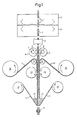
- each member of a series of substrate elements (boards) for printed circuits 1 is mechanically advanced in a continuous manner on a roller conveyor through cleaning chamber 3 in which both the upper and lower copper-clad surfaces thereof are cleaned by mechanically scrubbing under a heavy water spray.
- the boards are made of fiberglass-reinforced epoxy resin.
- the cleaned substrate boards are further advanced through alignment rolls 5, which are clean as defined by the Uniform Water Film test, by which the sides of the boards are precisely aligned. From the alignment rolls 5, each aligned substrate board emerges and is passed between liquid application rolls 6 into which thin layer liquid (in this case, 30% ethanol/water solution) is admitted via line 7 into the interior of the hollow application rolls 6.
- the application rolls 6 consists of a metal core perforated in a regular pattern having thereon a hard porous polyethylene sleeve which is covered with a cotton cloth through which the thin layer liquid passes and is coated onto the substrate boards.
- Liquid level within the application rolls 7 is limited by fixed level outlet line 8.
- the liquid layers have a thickness of 10 to 50 (lm.
- the board with both surfaces coated with a thin layer of liquid is then advanced to a set of upper and lower feed rolls 9 each of which places the unprotected surface of a continuous supported photosensitive layer 11 against the thin liquid layer on the substrate element.
- a preferred roller drive for advancing the substrate elements is disclosed in U.S. Patent 4,377,434.
- Optional feed rolls 9 place the photosensitive layers against the surfaces of the substrate element without any significant pressure just before the layer and substrate pass to the nip of the laminating rolls. Any excess liquid is removed from the substrate surface by forming a bead at the nip as the element passes between feed rolls 9. By this means moisture is retained between the liquid layer and substrate and thermal exposure is limited to the brief time it is within the nip. In the event of a stoppage, the amount of photosensitive layer subject to thermal degradation is reduced substantially.
- the feed rolls 9 are mechanically linked with the mechanism used for advancing the boards 1 in such manner that the boards are butted up against one another as they enter the feed rolls 9 and there is no significant amount of bridging by the film 11 between the trailing and leading edges of each board.
- the supported photosensitive layers prepared as described in Example 1 are supplied from supply rolls 12.
- the abutting boards 1 with the supported photosensitive layers 11 in place are then advanced through the nips of heated laminating rolls 13 in which the photosensitive layer 11 are subjected to both pressure and heat, by which the thin liquid layer is removed from the substrate by absorption into the photosensitive layer.
- the temperature of the laminating roll surfaces is about 110°C and the linear speed of the boards through the laminator is about 182,88 cm per minute. Lamination is completed within about 40 seconds after the board is cleaned.
- a preferred actuating crank mechanism for opening and closing the laminating rolls is disclosed in U.S. Patent 4,387,000.
- the laminated boards 1 still abutting each other, are advanced at a uniform rate between wedges 15.
- the poly(ethylene terephthalate) web 17 on the outer surface of the continuous film is pulled back uniformly from the substrate at an obtuse angle (here 150°) which causes the photosensitive layer to be trimmed in a straight line along the leading edge of the board 1).
- the web 17 is pulled back by the action of take-up rolls 19 and the advancing action of the board.
- a preferred mandrel slip clutch mechanism for maintaining proper tension on the take-up roll is disclosed in U.S. Patent 4,363,455.
- the laminated board is ready for circuit preparation by conventional photoresist techniques.
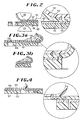
- Figure 2 is a schematic representation in cross-section of a preferred method of carrying out the lamination step of the invention in which after laydown of a thin liquid film 100, the photosensitive layer 102 adhered to support film 104 is laminated to substrate 106 which is coated with a thin layer of copper 107 by passage through laminating rolls 108 and 110.
- the strength of the adhesive bond (A z ) between the copper coating 107 of the substrate and the photosensitive layer 102 exceeds the strength of the adhesive bond (A,) between the photosensitive layer 102 and support 104.
- Figure 3 is a schematic representation in cross-section of the preferred method of trimming the front edge of laminate substrate 106 in which the advancing substrates in the series are spaced.
- the support 104 and photosensitive layer 102 are pulled back at an obtuse angle and small radius over wedge 112 so that the breaking strength (B) of the photosensitive layer 102 at the front edge of the substrate 106 is exceeded which causes breaking of layer 102 across the leading edge of substrate 106 as is shown in Figure 3B.
- a i is greater than A z which in turn is greater than B.
- Figure 4 is a schematic representation in cross-section of the method of trimming the trailing edge of laminated substrate 106 when the advancing substrates in the series are spaced.
- a longitudinal tensile stress perpendicular to the trailing edge i.e., parallel to and in the direction of travel, is applied by pulling on the leading edge of the substrate so thatthe breaking strength (B) of the photosensitive layer 102 along the trailing edge is exceeded.
- thermoplastic layer to be used in the process be relatively harder than most photosensitive layers.
- the hardness of the layer also makes the layer relatively brittle, i.e., under high shear, the layer loses strength apparently by a reduction in viscosity, whereby the layer exhibits dilatent character.
- the process takes advantage of this in that upon tensioning of the layer after lamination, the layer breaks along the substrate trailing edge and does not just elongate and fracture irregularly as would be the case with softer layers.
- the process is simultaneously practiced on both sides of the succession of substrates so that photopolymerizable layer is laminated to both sides of the substrates.
- the succession of substrates be close enough that the spring-loaded lamination rolls normally used for lamination do not "bottom" between substrates.
- a photosensitive coating mixture was prepared and coated as in Example 1 except that instead of the beads used therein, 16 parts by weight of 1 micrometer polyethylene beads (Microfine VIII-F. Gold, tradename of Dura Commodities Corporation, Harrison, NY) were dispersed in the coating solution.
- the surface of a 0.023 cm thick aluminum plate was scrubbed with tungsten carbide brushes in water using a Chemcut" Model 107 (tradename of Chemcut Corporation, State College, PA) Mechanical Cleaning System and the scrubbed surface was laminated to the photosensitive layer and the layer trimmed as described in Example I.
- the laminated and trimmed board was imaged by exposing for 60 seconds the photosensitive layer through a halftone and line transparency to U.V. radiation from 2000 watt pulsed Xenon arc light source in a flip top platemaker.
- the unexposed areas were completely removed by development in a 1% aqueous solution of sodium carbonate to provide a halftone polymeric image with complimentary image areas of bare aluminum surface.
- the resulting lithographic printing plate was conventionally gummed with Lydel @ Finishing Solution (LDFS) (tradename of E.I. du Pont de Nemours and Company, Wilmington, DE) and mounted on an A.B. Dick Model 380 offset printing press. Using standard inking and fountain solutions, at least 3500 copies of good quality were obtained from the printing plate.
- LDFS Lydel @ Finishing Solution
Description
- The invention relates to an integrated process for laminating a continuous layer of photosensitive composition to a surface of each member of a series of substrate elements and trimming the layer from at least one of the transverse edges of the laminated substrate elements.
- U.S. Patent 3,469,982 discloses a photoresist process comprising applying a photopolymerizable layer supported on a support film to a surface, followed by imagewise exposure of the layer, stripping away the support film, and washing away the unexposed area of the layer to leave a resist image protecting the aforesaid surface from such treatments as etching or plating.
- The patent discloses solution coating of a photopolymerizable composition onto the support film, followed by drying and then lamination of the resultant dry coating to a surface such as copper-clad printed circuit board (Example V) to carry out the photoresist process. In commercial practice, however, the dried photopolymerizable coating, which must remain adhered to the support during storage and shipment, has always been supplied sandwiched between the support film and a cover sheet, such as disclosed in Example I of the patent. This has enabled the sandwich to be rolled up upon itself by the photoresist manufacturer and be supplied to the user, e.g. printed circuit manufacturer, as a compact, easy to handle roll. The cover sheet permitted the roll to be unrolled by the user. Without the cover film, pressing the photopolymerizable layer against the backside of the support film would cause that layer to adhere. Consequently, the film could not be unrolled without damaging the photopolymerizable layer. In use, the cover sheet would be stripped away and discarded, followed by the photoresist processing described above. U.S. Patent 3,782,939 discloses a need for the cover sheet because of the alleged tackiness of the photopolymerizable layer. In fact, the layer need not be tacky to the touch, but can adhere under pressure, for example with it is rolled up.
- The equipment used to practise the photoresist process has consisted in general of separate pieces of equipment, such as a cleaner, scrubber for cleaning the copper-clad circuit boards, oven for preheating the boards, roll laminator applying heat to the photoresist and board as it laminates them together, and exposure (actinic radiation) station, and solvent development apparatus. Typically, manual transfer and positioning of the circuit board was necessary between each piece of equipment, involving expense and less-than-desired reproducibility leading to yield loss in the process.
- Various attempts have been made to automate the photoresist process but automation has been adopted to only a limited extent.
- U.S. Patent 3,547,730 discloses a process and apparatus for automating the photoresist process, involving a device for sequential feeding of shaped articles such as circuit boards and a laminator for receiving the boards and laminating a photosensitive layer thereto. Sequentially laminated boards become tied together by a web of support film and the photosensitive layer extending between boards as shown in Fig. 2, and the layer of the top and bottom web become laminated together to form a "hinge" (col. 5, lines 35-39). Next the support film is stripped away by
rolls - U.S. Patent 3,547,730 also discloses the cleaning of a circuit board between a feed station and lamination station, the preheating of the board and/or photosensitive layer between their respective feeds and the lamination station, and rolls 10 for stripping away the cover sheet prior to lamination.
- U.S. Patent 4,025,380 discloses the sequential feeding of circuit boards onto a conveyor which passes them through an infrared preheater and then past sensor switches which control the operation of laminating rolls and cutting devices which cut a photosensitive layer to the desired length prior to lamination and then laminate the cut sheet (layer) to the circuit board. The patent also discloses rolls 63 for stripping off of the cover film prior to the lamination.
- Improvements in specific process steps have been disclosed. U.S. Patent 3,629,036, discloses that the elevated temperature required for laminating a photoresist to a substrate introduces disadvantages of limiting the types of photoresist and substrate materials that can be used and produces inferior bonding to the substrate. The patent purports to solve these problems by room temperature lamination after first applying a solution of dissolved resist to the substrate and then doing the lamination. The patent provides for a release layer between the photoresist layer and its support film to enable the film to be stripped away from the photoresist layer after lamination.
- U.S. Patent 3,794,546 discloses the use of an adhesive web to adhere to a support film of a photohardenable element so as to delaminate the support film from at least the unhardened area of an image wise exposed photohardenable layer laminated to a receptor sheet.
- U.S. Patent 4,075,051 discloses a process for self trimming of a photoresist layer laminated to a substrate, i.e. the portion of the layer extending past the edges of the substrate without any cutting step. This is accomplished by applying a liquid weakening agent at leastto the aforesaid portion of the layer, but possibly to the entire layer by pre-wetting of the substrate with the agent, and then peeling away either the cover sheet (support film) or an auxiliary permeable sheet which has a greater adhesion to the layer than the cohesive strength (as a result of the weakening agent) of the layer. The portion of the layer extending past the edge of the substrate tears along the edge of the substrate by the action of peeling away the cover sheet or permeable sheet and is removed with the sheet. The weakening agent is either a solvent for the photoresist or is a softening agent for it. The patent discloses the use of a conventional roll type laminator and pressure and heat for adhering the photoresist layer to the substrate.
- Though the prior art methods of lamination are satisfactory for many applications, there is a need for even more precise and uniform lamination methods, especially where printed circuit boards having a very high line density are being fabricated. It further is desirable to avoid the use of the weakening agent.
- The invention is directed to an integrated process for laminating a continuous layer of photosensitive composition to a surface of each member of a series of substrate elements and trimming the layer from at least one of the transverse edges of the laminated substrate elements comprising the sequential steps of:
- (1) advancing a continuous layer of photosensitive organic polymeric composition, the layer being supported on one side by a strippable polymeric film, and advancing the continuous supported layer and a first substrate element to the nip of a set of laminating rolls;
- (2) contacting the unsupported surface of the supported layer with a surface of the substrate element within the nip under pressure to effect lamination of the layer to the surface of the substrate element;
- (3) removing the support film from the layer as the laminated substrate element emerges from the nip of the laminating.rolls and continuing advancement of the laminated substrate element until the support film is completely removed from the laminated layer;
- (4) pulling on the laminated substrate element along its longitudinal axis in the direction of advancement by which the breaking strength of the laminated layer is exceeded at the trailing edge of the substrate transversely to the direction of advancement; and
- (5) repeating the sequence of steps (2) through (4) which respect to subsequent substrate elements in the series.
- In a preferred aspect of the invention, the support film is removed from the layer as it emerges from the nip of the laminating rolls by bending the film back along the longitudinal axis of the advancing layer at an obtuse angle, the radius of the bend being sufficiently small that the breaking strength of the layer on the leading edge of the substrate element is exceeded.
- Further advantages and details of the invention will be apparent by reference to the Drawings which consists of four figures, as follows:
- Figure 1 is a schematic drawing which illustrates a preferred application of the process of the invention in a continuous laminating process; Figure 2 is a schematic drawing which illustrates in cross section a preferred method of substrate treatment prior to lamination of photosensitive layers thereto; Figures 3A and B are schematic drawings which illustrates in cross section a preferred method of trimming photosensitive layer from the leading edge of substrates laminated by this process; and Figure 4 is a schematic drawing which illustrates in cross section a preferred method of trimming photosensitive layer from the trailing edge of substrates laminated by the process of the invention.
- The invention may be used advantageously in the lamination of a broad spectrum of thermoplastic layers. The invention is particularly useful for the lamination of photosensitive resist elements to substrates which are to be used for making printed circuit boards. The invention is also useful for lamination of photosensitive layers to substrates in the preparation of lithographic printing plates.
- In practising the invention, photosensitive film resists of various types may be used. In general photohardenable, negative-working resists are photopolymerizable films of the type disclosed in U.S. Patent 3,469,982 and the photocrosslinkable elements of the type disclosed in U.S. Patent 3,526,504. Positive-working, resist elements may be of the photosolubilizable type, e.g., such as the o-quinone diazide elements of U.S. Patent 3,837,860, or of the photodesensitizable type, e.g., such as the bisdiazonium salts of U.S. Patent 3,778,270 or the nitroaromatic composition of U.K. Patent 1,547,548.
- The photosensitive layer used in the process is preferably aqueous alkali processible in the sense that it is soluble and thereby developable in aqueous alkali solution, e.g., 1 wt% Na2C03 at 29.4°C for 90 seconds at a spray pressure of 1.38 kg/cm2.
- An element containing an image-yielding, non-blocking photopolymerizable stratum on a strippable support is preferably used such as the one described in European Patent Application No. 81 103 965.0. Alternatively, particularly if the photopolymerizable layer is tacky, the remaining surface of the supported, photopolymerizable stratum may be protected by a removable cover sheet or when the element is stored in roll form, the stratum surface may be protected by the contiguous reverse surface of the support. The photosensitive composition is present in a dry coating thickness of about 0.0003 inch (-0.0008 cm) to about 0.01 inch (-0.025 cm) or more. A suitable strippable support which preferably has a high degree of dimensional stability to temperature changes, may be chosen from a wide variety of films composed of high polymers, e.g. polyamides, polyolefins, polyesters, vinyl polymers, and cellulose esters, and may have a thickness of from 0.00025 inch (-0.0006 cm) to 0.008 inch (-0.02 cm) or more. A particularly suitable support is a transparent polyethylene terephthalate film having a thickness of about 0.001 inch (-0.0025 cm).
- When the invention is used to laminate photosensitive layers, it is essential that the adhesion (A,) of the unexposed photosensitive layer to the polymeric support exceeds the breaking strength (B) of the unsupported photosensitive layer. Likewise, the adhesion (A2) of the unexposed photosensitive layer to the substrate must exceed the breaking strength (B) of the unsupported photosensitive layer. In addition, since the polymeric support must be strippable from the laminated photopolymerizable layer, the adhesion (A2) of the photolayer to the substrate must also exceed its adhesion (A,) to the polymeric support. Expressed methamatically, A2>A,>B. The proper balance of these adhesive and breaking forces in photosensitive systems can be provided by adjustment of the relative proportions of monomer and binder.
- As noted above, the photosensitive layer is also preferably compounded to be relatively hard and nonblocking, i.e., it will not stick to itself or the film support with a greater adhesive strength than the cohesive strength of the layer. The result of this is that a cover sheet is not necessary to prevent the layer from sticking to the support film while in the rolled-up condition for the photosensitive element. This provides a saving in material costs and eliminates the need for cover sheet stripping and disposal of the stripped cover sheet.
- When the element contains no removable, protective cover sheet and is to be stored in roll form, additional protection against blocking can optionally be provided if the reverse side of the strippable support has applied thereto a thin release layer of a material, such as wax or silicone, to prevent blocking with the photopolymerizable stratum. Alternatively, adhesion to the coated photopolymerizable layer may be preferentially increased by flame treating or electrical discharge treating the support surface to be coated.
- Suitable removable, protective cover sheets when used may be chosen from the same group of high polymer films described above and may have the same wide range of thicknesses. A cover sheet of 0.001 inch (-0.0025 cm) thick polyethylene is especially suitable. Supports and cover sheets as described above provide good protection to the photopolymerizable resist layer.
- The photohardenable layer is prepared from polymeric components (binders), monomeric components, initiators and inhibitors.
- Suitable binders which can be used as the sole binder or in combination with others include the following: polyacrylate and alpha-alkyl polyacrylate esters, e.g., polymethyl methacrylate and polyethyl methacrylate; polyvinyl esters, e.g., polyvinyl esters, e.g. polyvinyl acetate, polyvinyl acetate/acrylate, polyvinyl acetate/methacrylate and hydrolyzed polyvinyl acetate; ethylene/vinyl acetate copolymers; polystyrene polymers and copolymers, e.g., with maleic anhydride and esters; vinylidene chloride copolymers, e.g., vinylidene chloride/acrylonitrile; vinylidene chloride/methacrylate and vinylidene chloride/vinyl acetate copolymers, polyvinyl chloride and copolymers, e.g., polyvinyl chloride/acetate; saturated and unsaturated polyurethanes; synthetic rubbers, e.g. butadiene/acrylonitrile, acrylonitrile/buta- diene/styrene, methacrylate/acrylonitrile/butadiene/styrene copolymers, 2-chlorobutadiene-1,3 polymers, chlorinated rubber and styrene/butadiene/styrene, styrene/isoprene/styrene block copolymers; high molecular weight polyethylene oxides of polyglycols having average molecular weights from about 4,000 to 1,000,000; epoxides, e.g. epoxides containing acrylate or methacrylate groups; copolyesters, e.g., those prepared from the reaction product of a polymethylene glycol of the formula HO(CH2)nOH, where n is a whole number 2 to 10 inclusive, and (1) hexahydroterephthalic, sebacic and terephthalic acids, (2) terephthalic, isophthalic and sebacic acids, (3) terephthalic and sebacic acids, (4) terephthalic and isophthalic acids, and (5) mixtures of copolyesters prepared from said glycols and (i) terephthalic isophthalic and sebacid acids and (ii) terephthalic, isophthalic sebacic and adipic acids; nylons or polyamides, e.g., N-methoxymethyl polyhexamethylene adipamide; cellulose esters, e.g., cellulose acetate, cellulose acetate succinate and cellulose acetate butyrate; cellulose ethers, e.g., methyl cellulose, ethyl cellulose and benzyl cellulose; polycarbonates; polyvinyl acetal, e.g., polyvinyl butyral, polyvinyl formal; polyformaldehydes.
- Preferably, the binder should contain sufficient acidic or other groups to render the composition processible in aqueous developer as described hereinbefore. Useful aqueous-processible binders include those disclosed in U.S. Patent 3,458,311 and in U.K. 1,507,704. Useful amphoteric polymers include interpolymers derived from N-alkylacrylamides or methacrylamides, acidic film-forming comonomer and an alkyl or hydroalkyl acrylate such as those disclosed in U.S. Patent 3,927,199 which is incorporated herein by reference.
- It is preferred that the photosensitive layer be relatively harder than those which generally have been available before now. Greater hardness of the layer provides greater dimensional stability and thus there is less requirement for support by the support film.
- Suitable monomers which can be used as the sole monomer or in combination with others include the following: t-butyl acrylate, 1,5-pentanediol diacrylate, N,N-diethylaminoethyl acrylate, ethylene glycol diacrylate, 1,4-butanediol diacrylate, diethylene glycol diacrylate, hexamethylene glycol diacrylate, 1,3-propanediol diacrylate, decamethylene glycol diacrylate, decamethylene glycol dimethacrylate, 1,4-cyclohexane diol diacrylate, 2,2-dimethylolpropane diacrylate, glycerol diacrylate, tripropylene glycol diacrylate, glycerol triacrylate, trimethylolpropane triacrylate, pentaerythritol triacrylate, polyoxyethylated trimethylolpropane triacrylate and trimethacrylate and similar compounds as disclosed in U.S. Patent 3,380,831, 2,2-di(p-hydroxyphenyl)propane diacrylate, pentaerythritol tetraacrylate, 2,2-di-(p-hydroxyphenyl)propane dimethacrylate, triethylene glycol diacrylate, polyoxyethyl-2,2-di-(p-hydroxyphenylpropane dimethacrylate, di-(3-methacryloxy-2-hydroxypropyl) ether of bisphenol-A, di(2-methacryloxyethyl) ether of bisphenol-A, di(3-acryloxy-2-hydroxypropyl) ether of bisphenol-A, di(2-acryloxyethyl) ether of bisphenol-A, di(3-methacryloxy-2-hydroxypropyl) ether of tetrachloro-bisphenol-A, di(2-methacryloxyethyl)ether of tetrachloro-bisphenol-A, di-(3-methacryloxy-2-hydroxypropyl) ether of tetrabromo-bisphenol-A, di(2-methacryloxyethyl) ether of tetrabromo-bisphenol-A, di-(3-methacryloxy-2-hydroxypropyl) ether of 1,4-butanediol, di(3-methacryloxy-2-hydroxypropyl) ether of diphenolic acid, triethylene glycol dimethacrylate, polyoxypropyltrimethylol propane triacrylate (462) ethylene glycol dimethacrylate, butylene glycol dimethacrylate, 1,3-propanediol dimethacrylate, 1,2,4-butanetrio! . trimethacrylate, 2,2,4-trimethyl-1,3-pentanediol dimethacrylate, pentaerythritol trimethacrylate, 1-phenyl ethylene-1,2-dimethacrylate, pentaerythritol tetramethylacrylate, trimethylol propane trimethacrylate, 1,5-pentanediol dimethacrylate, diallyl fumarate, styrene, 1,4-benzenediol dimethacrylate, 1,4-diisopropenyl benzene, and 1,3,5-triisopropenyl benzene.
- In addition to the ethylenically unsaturated monomers mentioned above, the photohardenable layer can also contain at least one of the following free radical-initiated, chain-propagating, addition- polymerizable, ethylenically unsaturated compounds having a molecular weight of at least 300. Preferred monomers of this type are an alkylene or a polyalkylene glycol diacrylate prepared from an alkylene glycol of 2 to 15 carbons or a polyalkylene ether glycol of 1 to 10 ether linkages, and those disclosed in U.S. Patent 2,927,022, e.g., those having a plurality of addition polymerizable ethylenic linkages particularly when present as terminal linkages. Especially preferred are those wherein at least one and preferably most of such linkages are conjugated with a double bonded carbon, including carbon double bonded to carbon and to such heteroatoms as nitrogen, oxygen and sulfur. Outstanding are such materials wherein the ethylenically unsaturated groups, especially the vinylidene groups, are conjugated with ester or amide structures.
- Preferred free radical-generating addition-polymerization initiators activatable by actinic light and thermally inactive at and below 185°C include the substituted or unsubstituted polynuclear quinones which are compounds having two intracyclic carbon atoms in a conjugated carbocyclic ring system e.g., 9, 10- anthraquinone, 1-chloroanthraquinone, 2-chloroanthraquinone, 2-methylanthraquinone, 2-ethylanthraquinone, 2-tert-butylanthraquinone, octamethylanthraquinone, 1,4-naphthoquinone, 9,10-phenanthrenequinone, 1,2-benzanthraquinone, 2,3-benzanthraquinone, 2-methyl-1,4-naphthoquinone, 2,3-dichloronaphthoquinone, 1,4-dimethyianthraquinone, 2,3-dimethylanthraquinone, 2-phenylanthraquinone, 2,3-diphenylanthraquinone, sodium salt of anthraquinone alpha-sulfonic acid, 3-chloro-2-methylanthraquinone, retenequinone, 7,8,9,10-tetrahydronaphthacenequinone, and 1,2,3,4-tetrahydrobenz(a)anthracene-7,12-dione. Other photoinitiators which are also useful, even those some may be thermally active at temperatures as low as 85°C, are described in U.S. Patent 2,760,863 and include vicinal ketaldonyl alcohols, such as benzoin, pivaloin, acyloin ethers, e.g., benzoin methyl and ethyl ethers; a-hydrocarbon-substituted aromatic acyloins, including a-methylbenzoin, a-allylbenzoin and a-phenylbenzoin. Photoreducible dyes and reducing agents disclosed in U.S. Patents: 2,850,445; 2,875,047; 3,097,096; 3,074,974; 3,097,097; and 3,145,104 as well as dyes of the phenazine, oxazine, and quinone classes; Michler's ketone, benzophenone, 2,4,5-triphenyl-imidazolyl dimers with hydrogen donors, and mixtures thereof as described in U.S. Patents: 3,427,161; 3,479,185; and 3,549,367 can be used as initiators. Also useful with photoinitiators and photoinhibitors are sensitizers disclosed in U.S. Patent 4,162,162.
- Thermal polymerization inhibitors that can be used in photopolymerizable compositions are: p-methoxyphenol, hydroquinone, and alkyl and aryl-substituted hydroquinones and quinones, tert-butyl catechol, pyrogallol, copper resinate, naphthylamines, beta-naphthol, cuprous chloride, 2,6-di-tert-butyl-p-cresol, phenothiazine, pyridine, nitrobenzene and dinitrobenzene, p-toluquinone and chloranil. Also useful for thermal polymerization inhibitors are the nitroso compositions disclosed in U.S. 4,168,982.
- Various dyes and pigments may be added to increase the visibility of the resist image. Any colorant used, however, should preferably be transparent to the actinic radiation used.
- Generally, suitable substrates for the process of the invention involving printed circuit formation are those which have mechanical strength, chemical resistance and good dielectric properties. Thus, most board materials for printed circuits are thermosetting or thermoplastic resins usually combined with a reinforcing agent. Thermosetting resins with reinforcing fillers are ordinarily used for rigid boards, whereas thermoplastic resin without reinforcements are usually used for flexible circuit boards. Ceramic and dielectric coated metals are also useful.
- Typical board construction involves combinations such as phenolic or epoxy resins on paper or a paper-glass composite, as well as polyester, epoxy, polyimide, polytetrafluorethylene, or polystyrene on glass. In most instances, the board is clad with a thin layer of electroconductive metal of which copper is by far the most common.
- Suitable substrates for the process of the invention involving preparation of lithographic printing plates are those which have mechanical strength and surfaces which differ in hydrophilicity or oleophilicity from the surfaces of the images photosensitive areas laminated thereto. Such substrates are disclosed in U.S. Patent 4,072,528. While numerous substrates are satisfactory for this purpose thin anodized aluminum plates such as disclosed in U.S. Patent 3,458,311 are particularly useful.
- As noted above, the adhesion of the unexpected photosensitive layer to substrates such as copper or aluminum (AZ) must be greater than its breaking strength (B) and its adhesion to the support (A1). A high value for A2 is also needed for many of the applications of this invention where the photosensitive layer must remain adhered to the substrate during exposure to severe chemical or mechanical conditions.
- It is essential that the printed circuit substrates used be clean and free of any extraneous materials to insure that these materials do not interfere with wetting and bonding of the surface. For this reason, it will frequently be desired to clean printed circuit substrates prior to lamination by one or more of the several cleaning processes which are well-known in the field of printed circuit board manufacture. The particular type of cleaning depends upon the type of contamination - organic, particulate or metallic. Such methods include degreasing with solvents and solvent emulsions, mechanical scrubbing, alkaline soaks, acidification and the like, followed by rinsing and drying.
- Suitable cleanliness can be very easily determined by the Uniform Water Film test in which the substrate is dipped into water, removed from the water and then the board surface is observed. If a uniform film of water is observed, the board is adequately clean but if a discontinuous streaked film or large droplets are formed, the board is not sufficiently clean to be used in the process of the invention.
- In the process of the invention, the thermoplastic layer is laminated to the substrate by means of nip rolls. For most applications, and particularly in the manufacture of printed circuit boards from conventional photoresist elements, it is necessary to laminate the photosensitive layer of the element to the substrate board in such manner that the layer is firmly adhered thereto without occlusions and other phase discontinuities such as entrapped air or liquids. Cleaned surfaces tend to deteriorate rapidly immediately after cleaning, e.g., by oxidation or dust. Therefore in a preferred method of practicing the invention, the surface of the substrate, just prior to lamination, is treated to improve adhesion between the photosensitive layer and the substrate by the sequential steps of:
- (a) applying a thin layer of inert liquid to the substrate surface immediately prior to lamination of the photosensitive layer thereto; and
- (b) removing the thin layer of liquid from the substrate surface by vaporization and/or absorption into the photosensitive layer.
- In corresponding European Patent Application No. 81 103 9995.7 the inert liquid is a nonsolvent with respect to the thermoplastic layer. In a related treating method disclosed in European Patent Application No. 81 103 965.0 the thin layer of inert liquid is applied to the substrate surface by contacting the surface at a temperature below the condensation point of the liquid with a vapor or gaseous dispersion of the liquid. The inert liquid used to form the film can also be applied in other ways, for example, by brushing, wicking, atomizing spray or by rolling it on using perforated or porous rolls.
- The thin liquid layer should cover at least 30 percent of the substrate surface on which the polymer is to be laminated and preferably at least 80 percent. Essentially complete coverage is still further preferred.
- Since this invention is integrated into a continuous process in which the support film is removed shortly after lamination, the liquid layer should be sufficiently thin for adhesion to the substrate to occur almost instantaneously. Thus, the liquid should not flood the surface of the substrate such as described in U.S. Patent 4,069,076. Excess liquid interferes with instant adhesion and furthermore fills the interconnective holes which are normally present in a printed circuit substrate and thereby acts as a contaminant in subsequent processing operations.
- In practice, it is preferred that the thin liquid layer be as thin as is practicable to displace air at the interface and promote adhesion of the photosensitive layer. While the particular layer thickness will vary somewhat, depending upon the nature of the liquid and the conditions of application, it is generally preferred that it be much thinner than in the prior art proccesses, e.g., from 1-50 pm, the average layer thickness being about 30 ¡..lm or a preferred range from about 10 to about 50 pm.
- It is an essential aspect of the substrate treatment that the applied thin liquid film be substantially displaced from the interface between the photosensitive layer and the substrate during the subsequent laminating operation. This is done mainly by diffusion into the laminated polymeric layer. The precise method by which the thin liquid film is displaced is, of course, a function of the liquid and the nature of the photosensitive layer and substrate which are used. When a more volatile liquid is used in conjunction with heated laminating rolls, liquid film displacement may take place partially by vaporization. On the other hand, using a less volatile liquid and/or cooler rolls will result in less volatilization and thus removal of the liquid film will occur to a greater extent by absorption into the laminated polymer layer. Obviously, when nonvolatile liquids are used, the removal of the liquid film takes place essentially by absorption. The precise mechanism by which the liquid film is removed is not critical.
- With the above-described thin film treatment, even relatively hard thermoplastic layers can be adhered to substrates effectively. Of course, the substrate has to be clean. Integration of the cleaning operation with the laminating operation provides the required cleanliness. Without the presence of this film during lamination the layer may not instantly adhere to the substrate.
- It is preferred that the precleaning operation be carried out in the integrated manner described in European Patent Application No. 81 103 966.8.
- When the advancing substrate elements are butted against each other in such manner that there is no significant space between the trailing edge of the leading board and the leading edge of the following board, a single application of longitudinal tensile stress operates to trim the layer simultaneously from both the trailing edge of the leading board and the leading edge of the following board. On the other hand, when successive boards are spaced in such manner that there is a "bridge" of photosensitive layer spanning the gap between the trailing edge of the leading board and the leading edge of the following board, it is necessary to trim the two edges separately. In this case, the tensile stress to trim the leading edge of the boards is applied preferably by removing the support film from the layer as the laminated substrate element emerges from the nip of the laminating rolls by bending the film back along the longitudinal axis of the advancing layer at an obtuse angle, the radius of the bend being sufficiently small that the breaking strength of the layer on the leading edge of the substrate element is exceeded.
- The invention will be more clearly understood by reference to the following examples and the detailed description of the Drawing hereinbelow.
- A roll of photoresist film having no cover sheet is prepared as follows:
- A photosensitive coating solution is prepared having the following composition:Into the above coating solution are dispersed 13 parts by weight of polyethylene beads of which 85% have diameters below 10 pm and 15% have diameters between 10 and 20 µm. The mixture is coated on a 0.00127 cm thick polyethylene terephthalate web which has coated on its reverse side a thin layer of a mixture of Carnuba wax and poly(vinylidene chloride). The photopolymerizable layer is dried to give a dry thickness of 0.00254 cm and about 30.5 meters of the dried coated element is wound into a roll.

- Turning now to Figure 1 of the drawing, each member of a series of substrate elements (boards) for printed circuits 1 is mechanically advanced in a continuous manner on a roller conveyor through cleaning
chamber 3 in which both the upper and lower copper-clad surfaces thereof are cleaned by mechanically scrubbing under a heavy water spray. The boards are made of fiberglass-reinforced epoxy resin. The cleaned substrate boards are further advanced through alignment rolls 5, which are clean as defined by the Uniform Water Film test, by which the sides of the boards are precisely aligned. From the alignment rolls 5, each aligned substrate board emerges and is passed between liquid application rolls 6 into which thin layer liquid (in this case, 30% ethanol/water solution) is admitted via line 7 into the interior of the hollow application rolls 6. Preferably the application rolls 6 consists of a metal core perforated in a regular pattern having thereon a hard porous polyethylene sleeve which is covered with a cotton cloth through which the thin layer liquid passes and is coated onto the substrate boards. Liquid level within the application rolls 7 is limited by fixedlevel outlet line 8. The liquid layers have a thickness of 10 to 50 (lm. The board with both surfaces coated with a thin layer of liquid is then advanced to a set of upper and lower feed rolls 9 each of which places the unprotected surface of a continuous supported photosensitive layer 11 against the thin liquid layer on the substrate element. A preferred roller drive for advancing the substrate elements is disclosed in U.S. Patent 4,377,434. - Optional feed rolls 9 place the photosensitive layers against the surfaces of the substrate element without any significant pressure just before the layer and substrate pass to the nip of the laminating rolls. Any excess liquid is removed from the substrate surface by forming a bead at the nip as the element passes between feed rolls 9. By this means moisture is retained between the liquid layer and substrate and thermal exposure is limited to the brief time it is within the nip. In the event of a stoppage, the amount of photosensitive layer subject to thermal degradation is reduced substantially.
- The feed rolls 9 are mechanically linked with the mechanism used for advancing the boards 1 in such manner that the boards are butted up against one another as they enter the feed rolls 9 and there is no significant amount of bridging by the film 11 between the trailing and leading edges of each board. The supported photosensitive layers prepared as described in Example 1 are supplied from supply rolls 12. The abutting boards 1 with the supported photosensitive layers 11 in place are then advanced through the nips of heated laminating rolls 13 in which the photosensitive layer 11 are subjected to both pressure and heat, by which the thin liquid layer is removed from the substrate by absorption into the photosensitive layer. The temperature of the laminating roll surfaces is about 110°C and the linear speed of the boards through the laminator is about 182,88 cm per minute. Lamination is completed within about 40 seconds after the board is cleaned. A preferred actuating crank mechanism for opening and closing the laminating rolls is disclosed in U.S. Patent 4,387,000.
- The laminated boards 1 still abutting each other, are advanced at a uniform rate between
wedges 15. At the exit of thewedges 15, the poly(ethylene terephthalate)web 17 on the outer surface of the continuous film is pulled back uniformly from the substrate at an obtuse angle (here 150°) which causes the photosensitive layer to be trimmed in a straight line along the leading edge of the board 1). Theweb 17 is pulled back by the action of take-up rolls 19 and the advancing action of the board. A preferred mandrel slip clutch mechanism for maintaining proper tension on the take-up roll is disclosed in U.S. Patent 4,363,455. - As the substrate board 1 emerges from between
wedges 15 progressively more of the photosensitive layer is uncovered until the board advances to and is grasped firmly at the sides between a pair of clutch- driven trimming rolls 21, which rotate at a speed faster than the linear speed of the advancing board until they grasp the panel sides. The trimming rolls then move with the linear speed of the board by means of a slip clutch which compensates for the difference in driving speeds. The trimming rolls 21 place a tensile stress on the layers which causes the thermoplastic layers to be trimmed smoothly along the trailing edge of the board as it emerges from between thewedges 15. An alternative and further preferred means for grasping the laminated and trimmed substrate element is disclosed in U.S. Patent 4,338,152. - When the trailing edge trimming is completed, thus separating the leading and trailing boards in the series, the laminated board is ready for circuit preparation by conventional photoresist techniques.
- Figure 2 is a schematic representation in cross-section of a preferred method of carrying out the lamination step of the invention in which after laydown of a
thin liquid film 100, thephotosensitive layer 102 adhered to supportfilm 104 is laminated tosubstrate 106 which is coated with a thin layer ofcopper 107 by passage through laminating rolls 108 and 110. The strength of the adhesive bond (Az) between thecopper coating 107 of the substrate and thephotosensitive layer 102 exceeds the strength of the adhesive bond (A,) between thephotosensitive layer 102 andsupport 104. - Figure 3 is a schematic representation in cross-section of the preferred method of trimming the front edge of
laminate substrate 106 in which the advancing substrates in the series are spaced. Upon emergence from the laminating rolls, thesupport 104 andphotosensitive layer 102 are pulled back at an obtuse angle and small radius overwedge 112 so that the breaking strength (B) of thephotosensitive layer 102 at the front edge of thesubstrate 106 is exceeded which causes breaking oflayer 102 across the leading edge ofsubstrate 106 as is shown in Figure 3B. For this operation, Ai is greater than Az which in turn is greater than B. - Figure 4 is a schematic representation in cross-section of the method of trimming the trailing edge of
laminated substrate 106 when the advancing substrates in the series are spaced. As the support is removed from the trailing edge ofsubstrate 106, a longitudinal tensile stress perpendicular to the trailing edge, i.e., parallel to and in the direction of travel, is applied by pulling on the leading edge of the substrate so thatthe breaking strength (B) of thephotosensitive layer 102 along the trailing edge is exceeded. - Though the process of the invention as described above is carried out continuously, it will be recognized that the process can also be conducted intermittently as well.
- It is preferred that the thermoplastic layer to be used in the process be relatively harder than most photosensitive layers. The hardness of the layer also makes the layer relatively brittle, i.e., under high shear, the layer loses strength apparently by a reduction in viscosity, whereby the layer exhibits dilatent character. The process takes advantage of this in that upon tensioning of the layer after lamination, the layer breaks along the substrate trailing edge and does not just elongate and fracture irregularly as would be the case with softer layers.
- In a preferred aspect, the process is simultaneously practiced on both sides of the succession of substrates so that photopolymerizable layer is laminated to both sides of the substrates. In this instance, it is especially important that no liquid be present in the holes in the substrate, lest the heat of lamination vaporize the liquid and cause the "tents" of photosensitive layer over the holes in the substrate to expand and burst. It is also preferred that the succession of substrates be close enough that the spring-loaded lamination rolls normally used for lamination do not "bottom" between substrates. This avoids bonding together of the two photopolymerizable layers extending between the successive substrates, that is the "hinges" between successive substrates, since such bonding is likely to interfere with self-trimming of the leading edge when the support films are removed. Alternatively, the pressure on the lamination rolls can be reduced to minimize bonding of the layers. It is preferred, however, that "hinging" itself be kept to a minimum to facilitate the self-trimming function.
- A photosensitive coating mixture was prepared and coated as in Example 1 except that instead of the beads used therein, 16 parts by weight of 1 micrometer polyethylene beads (Microfine VIII-F. Gold, tradename of Dura Commodities Corporation, Harrison, NY) were dispersed in the coating solution. The surface of a 0.023 cm thick aluminum plate was scrubbed with tungsten carbide brushes in water using a Chemcut" Model 107 (tradename of Chemcut Corporation, State College, PA) Mechanical Cleaning System and the scrubbed surface was laminated to the photosensitive layer and the layer trimmed as described in Example I.
- The laminated and trimmed board was imaged by exposing for 60 seconds the photosensitive layer through a halftone and line transparency to U.V. radiation from 2000 watt pulsed Xenon arc light source in a flip top platemaker. The unexposed areas were completely removed by development in a 1% aqueous solution of sodium carbonate to provide a halftone polymeric image with complimentary image areas of bare aluminum surface. The resulting lithographic printing plate was conventionally gummed with Lydel@ Finishing Solution (LDFS) (tradename of E.I. du Pont de Nemours and Company, Wilmington, DE) and mounted on an A.B. Dick Model 380 offset printing press. Using standard inking and fountain solutions, at least 3500 copies of good quality were obtained from the printing plate.
Claims (11)
Priority Applications (1)
| Application Number | Priority Date | Filing Date | Title |
|---|---|---|---|
| AT81104013T ATE9410T1 (en) | 1980-05-27 | 1981-05-25 | INTEGRATED LAMINATION PROCESS. |
Applications Claiming Priority (4)
| Application Number | Priority Date | Filing Date | Title |
|---|---|---|---|
| US15363480A | 1980-05-27 | 1980-05-27 | |
| US153634 | 1980-05-27 | ||
| US06/244,792 US4378264A (en) | 1980-05-27 | 1981-03-27 | Integrated laminating process |
| US244792 | 1981-03-27 |
Publications (4)
| Publication Number | Publication Date |
|---|---|
| EP0041642A2 EP0041642A2 (en) | 1981-12-16 |
| EP0041642A3 EP0041642A3 (en) | 1982-02-17 |
| EP0041642B1 EP0041642B1 (en) | 1984-09-12 |
| EP0041642B2 true EP0041642B2 (en) | 1987-09-02 |
Family
ID=26850721
Family Applications (1)
| Application Number | Title | Priority Date | Filing Date |
|---|---|---|---|
| EP81104013A Expired EP0041642B2 (en) | 1980-05-27 | 1981-05-25 | Integrated laminating process |
Country Status (9)
| Country | Link |
|---|---|
| US (1) | US4378264A (en) |
| EP (1) | EP0041642B2 (en) |
| BR (1) | BR8103223A (en) |
| CA (1) | CA1169347A (en) |
| DD (1) | DD159225A5 (en) |
| DE (1) | DE3165976D1 (en) |
| HU (1) | HU181618B (en) |
| IE (1) | IE52117B1 (en) |
| PL (1) | PL231362A1 (en) |
Families Citing this family (43)
| Publication number | Priority date | Publication date | Assignee | Title |
|---|---|---|---|---|
| US4460427A (en) * | 1981-09-21 | 1984-07-17 | E. I. Dupont De Nemours And Company | Process for the preparation of flexible circuits |
| US4504566A (en) * | 1982-11-01 | 1985-03-12 | E. I. Du Pont De Nemours And Company | Single exposure positive contact multilayer photosolubilizable litho element with two quinone diazide layers |
| US4495014A (en) * | 1983-02-18 | 1985-01-22 | E. I. Du Pont De Nemours And Company | Laminating and trimming process |
| GB2157193B (en) * | 1984-04-10 | 1987-08-19 | Nitto Electric Ind Co | Process for peeling protective film off a thin article |
| CA1263125A (en) * | 1984-06-01 | 1989-11-21 | Hans-Guenter E. Kuehnert | Apparatus for the automatic feeding of a laminating station |
| DE3420429A1 (en) * | 1984-06-01 | 1985-12-05 | ELTI Apparatebau und Elektronik GmbH, 6106 Erzhausen | METHOD FOR LAMINATING A FILM UNDER PRESSURE AND HEAT, AND DEVICE FOR CARRYING OUT THE METHOD |
| DE3420409A1 (en) * | 1984-06-01 | 1985-12-05 | ELTI Apparatebau und Elektronik GmbH, 6106 Erzhausen | LAMINATION STATION |
| US4592816A (en) | 1984-09-26 | 1986-06-03 | Rohm And Haas Company | Electrophoretic deposition process |
| DE3510852A1 (en) * | 1985-03-26 | 1986-10-09 | ELTI Apparatebau und Elektronik GmbH, 6106 Erzhausen | GRIPPER DEVICE IN A LAMINATING DEVICE |
| DE3538117A1 (en) * | 1985-10-26 | 1987-04-30 | Hoechst Ag | DISCONNECTING DEVICE FOR PLATES |
| US4744847A (en) * | 1986-01-29 | 1988-05-17 | E. I. Du Pont De Nemours And Company | Film trimming of laminated photosensitive layer |
| US4839261A (en) * | 1986-09-29 | 1989-06-13 | Asahi Kasei Kogyo Kabushiki Kaisha | Photocurable laminate |
| US4714504A (en) * | 1986-10-10 | 1987-12-22 | Ibm Corporation | Process of laminating a photosensitive layer of a substrate |
| DE3736509A1 (en) * | 1987-10-28 | 1989-05-11 | Hoechst Ag | DEVICE FOR LAMINATING AND CUTTING PHOTORIST RESISTANT FILMS |
| JPH01160085A (en) * | 1987-12-16 | 1989-06-22 | Somar Corp | Method and device for applying thin film |
| JPH01160084A (en) * | 1987-12-17 | 1989-06-22 | Somar Corp | Method and device for applying thin film |
| JPH0659965B2 (en) * | 1988-01-30 | 1994-08-10 | ソマール株式会社 | Thin film sticking device |
| US4981549A (en) * | 1988-02-23 | 1991-01-01 | Mitsubishi Kinzoku Kabushiki Kaisha | Method and apparatus for growing silicon crystals |
| ATE131777T1 (en) * | 1988-04-04 | 1996-01-15 | Somar Corp | DEVICE FOR JOINING THIN FILM |
| DE68912426T2 (en) * | 1988-06-21 | 1994-05-11 | Gec Avery Ltd | Manufacture of portable electronic cards. |
| US4976817A (en) * | 1988-12-09 | 1990-12-11 | Morton International, Inc. | Wet lamination process and apparatus |
| US4971894A (en) * | 1989-02-13 | 1990-11-20 | International Business Machines Corporation | Method and structure for preventing wet etchant penetration at the interface between a resist mask and an underlying metal layer |
| JPH0651360B2 (en) * | 1989-06-04 | 1994-07-06 | ソマール株式会社 | Method and device for attaching thin film |
| US6001893A (en) * | 1996-05-17 | 1999-12-14 | Datacard Corporation | Curable topcoat composition and methods for use |
| US6268109B1 (en) | 1999-10-12 | 2001-07-31 | E. I. Du Pont De Nemours And Company | Composite photosensitive element |
| US6400589B2 (en) * | 2000-01-12 | 2002-06-04 | Toyota Jidosha Kabushiki Kaisha | Control apparatus for a power supply circuit including plural converter |
| US8065795B2 (en) | 2001-03-08 | 2011-11-29 | Ppg Industries Ohio, Inc | Multi-layer circuit assembly and process for preparing the same |
| US7000313B2 (en) * | 2001-03-08 | 2006-02-21 | Ppg Industries Ohio, Inc. | Process for fabricating circuit assemblies using electrodepositable dielectric coating compositions |
| US6713587B2 (en) | 2001-03-08 | 2004-03-30 | Ppg Industries Ohio, Inc. | Electrodepositable dielectric coating compositions and methods related thereto |
| US6951707B2 (en) * | 2001-03-08 | 2005-10-04 | Ppg Industries Ohio, Inc. | Process for creating vias for circuit assemblies |
| US7228623B2 (en) * | 2001-03-08 | 2007-06-12 | Ppg Industries Ohio, Inc. | Process for fabricating a multi layer circuit assembly |
| US6671950B2 (en) | 2001-03-08 | 2004-01-06 | Ppg Industries Ohio, Inc. | Multi-layer circuit assembly and process for preparing the same |
| JP2003320764A (en) * | 2002-02-27 | 2003-11-11 | Tokushu Paper Mfg Co Ltd | Slip sheet for lithographic printing plate and method for manufacturing it |
| CN1672475B (en) * | 2002-06-27 | 2011-11-23 | Ppg工业俄亥俄公司 | Single or multi-layer printed circuit board with recessed or extended breakaway tabs and method of manufacture thereof |
| US20060213685A1 (en) * | 2002-06-27 | 2006-09-28 | Wang Alan E | Single or multi-layer printed circuit board with improved edge via design |
| US6824959B2 (en) * | 2002-06-27 | 2004-11-30 | Ppg Industries Ohio, Inc. | Process for creating holes in polymeric substrates |
| US7297209B2 (en) * | 2003-12-18 | 2007-11-20 | Nitto Denko Corporation | Method and device for transferring anisotropic crystal film from donor to receptor, and the donor |
| JP2005221743A (en) * | 2004-02-05 | 2005-08-18 | Hitachi Chem Co Ltd | Photosensitive resin composition, photosensitive element using the same, method for producing resist pattern and method for producing printed wiring board |
| US7252733B2 (en) * | 2004-05-04 | 2007-08-07 | Eastman Kodak Company | Polarizer guarded cover sheet with adhesion promoter |
| US7887667B2 (en) * | 2008-05-08 | 2011-02-15 | Neenah Paper, Inc. | Heat transfer materials and methods of making and using the same |
| KR101511584B1 (en) * | 2008-09-25 | 2015-04-13 | 해성디에스 주식회사 | Feeding Apparatus for roll to roll manufacturing and feeding method for same |
| CN105667055B (en) * | 2016-01-14 | 2018-02-09 | 朗华全能自控设备(上海)股份有限公司 | A kind of base material and the pressing system and process for pressing of cover layer pressing |
| EP4308382A1 (en) * | 2021-03-17 | 2024-01-24 | Automatic Lamination Technologies S.R.L. | Laminator device for pliable sheet semi-finished products and method for producing said pliable semi-finished products |
Family Cites Families (10)
| Publication number | Priority date | Publication date | Assignee | Title |
|---|---|---|---|---|
| US3261686A (en) * | 1963-04-23 | 1966-07-19 | Du Pont | Photopolymerizable compositions and elements |
| US3498788A (en) * | 1966-07-05 | 1970-03-03 | Polaroid Corp | Novel laminations for identification cards |
| US3469982A (en) * | 1968-09-11 | 1969-09-30 | Jack Richard Celeste | Process for making photoresists |
| US3615448A (en) * | 1969-01-14 | 1971-10-26 | Grace W R & Co | Lithographic printing plate and method of preparation |
| US3629036A (en) * | 1969-02-14 | 1971-12-21 | Shipley Co | The method coating of photoresist on circuit boards |
| US3785817A (en) * | 1970-10-05 | 1974-01-15 | A Kuchta | Transfer of photopolymer images by irradiation |
| US3775112A (en) * | 1971-06-10 | 1973-11-27 | Eastman Kodak Co | Photopolymerizable material containing starch and process of using |
| DE2634560A1 (en) * | 1976-07-31 | 1978-02-02 | Hoechst Ag | METHOD AND DEVICE FOR DISCONNECTING CONNECTED |
| US4069076A (en) * | 1976-11-29 | 1978-01-17 | E. I. Du Pont De Nemours And Company | Liquid lamination process |
| US4075051A (en) * | 1976-11-29 | 1978-02-21 | E. I. Du Pont De Nemours And Company | Method of trimming photoresist film |
-
1981
- 1981-03-27 US US06/244,792 patent/US4378264A/en not_active Expired - Lifetime
- 1981-05-25 DE DE8181104013T patent/DE3165976D1/en not_active Expired
- 1981-05-25 IE IE1163/81A patent/IE52117B1/en unknown
- 1981-05-25 BR BR8103223A patent/BR8103223A/en unknown
- 1981-05-25 EP EP81104013A patent/EP0041642B2/en not_active Expired
- 1981-05-26 HU HU811577A patent/HU181618B/en unknown
- 1981-05-26 CA CA000378301A patent/CA1169347A/en not_active Expired
- 1981-05-27 DD DD81230331A patent/DD159225A5/en unknown
- 1981-05-27 PL PL23136281A patent/PL231362A1/xx unknown
Also Published As
| Publication number | Publication date |
|---|---|
| IE811163L (en) | 1981-11-27 |
| EP0041642A2 (en) | 1981-12-16 |
| BR8103223A (en) | 1982-02-16 |
| DD159225A5 (en) | 1983-02-23 |
| US4378264A (en) | 1983-03-29 |
| EP0041642A3 (en) | 1982-02-17 |
| DE3165976D1 (en) | 1984-10-18 |
| PL231362A1 (en) | 1982-02-01 |
| CA1169347A (en) | 1984-06-19 |
| IE52117B1 (en) | 1987-06-24 |
| EP0041642B1 (en) | 1984-09-12 |
| HU181618B (en) | 1983-10-28 |
Similar Documents
| Publication | Publication Date | Title |
|---|---|---|
| EP0041642B2 (en) | Integrated laminating process | |
| US4405394A (en) | Laminating process | |
| EP0117483B1 (en) | Laminating and trimming process | |
| EP0040843B1 (en) | Laminating process | |
| EP0041640A2 (en) | Photopolymerizable composition | |
| EP0040842B1 (en) | Laminating process | |
| CA1247441A (en) | Controlled roughening of a photosensitive composition | |
| EP0041643B1 (en) | Self-trimming photosensitive layer | |
| JPS6125146B2 (en) | ||
| EP0041639B1 (en) | Laminating process | |
| EP0193621B1 (en) | Photopolymerizable compositions and elements containing acid to reduce scum and stain formation | |
| US4631246A (en) | Uniform cover sheet with rough surface in a photosensitive element | |
| EP0091693B1 (en) | Improved cover sheet in a photosensitive element | |
| US4567128A (en) | Cover sheet in a photosensitive element | |
| JPH0222372B2 (en) | ||
| EP0092783A2 (en) | Photosensitive coatings containing crosslinked beads |
Legal Events
| Date | Code | Title | Description |
|---|---|---|---|
| PUAI | Public reference made under article 153(3) epc to a published international application that has entered the european phase |
Free format text: ORIGINAL CODE: 0009012 |
|
| PUAL | Search report despatched |
Free format text: ORIGINAL CODE: 0009013 |
|
| 17P | Request for examination filed |
Effective date: 19810525 |
|
| AK | Designated contracting states |
Designated state(s): AT BE CH DE FR GB IT LU NL SE |
|
| AK | Designated contracting states |
Designated state(s): AT BE CH DE FR GB IT LU NL SE |
|
| ITF | It: translation for a ep patent filed |
Owner name: ING. C. GREGORJ S.P.A. |
|
| GRAA | (expected) grant |
Free format text: ORIGINAL CODE: 0009210 |
|
| AK | Designated contracting states |
Designated state(s): AT BE CH DE FR GB IT LI LU NL SE |
|
| REF | Corresponds to: |
Ref document number: 9410 Country of ref document: AT Date of ref document: 19840915 Kind code of ref document: T |
|
| REF | Corresponds to: |
Ref document number: 3165976 Country of ref document: DE Date of ref document: 19841018 |
|
| ET | Fr: translation filed | ||
| PGFP | Annual fee paid to national office [announced via postgrant information from national office to epo] |
Ref country code: BE Payment date: 19841231 Year of fee payment: 5 |
|
| PG25 | Lapsed in a contracting state [announced via postgrant information from national office to epo] |
Ref country code: LU Free format text: LAPSE BECAUSE OF NON-PAYMENT OF DUE FEES Effective date: 19850531 |
|
| PLBI | Opposition filed |
Free format text: ORIGINAL CODE: 0009260 |
|
| 26 | Opposition filed |
Opponent name: BASF AKTIENGESELLSCHAFT Effective date: 19850612 |
|
| NLR1 | Nl: opposition has been filed with the epo |
Opponent name: BASF AKTIENGESELLSCHAFT |
|
| PGFP | Annual fee paid to national office [announced via postgrant information from national office to epo] |
Ref country code: AT Payment date: 19860304 Year of fee payment: 6 |
|
| PGFP | Annual fee paid to national office [announced via postgrant information from national office to epo] |
Ref country code: NL Payment date: 19870531 Year of fee payment: 7 |
|
| PUAH | Patent maintained in amended form |
Free format text: ORIGINAL CODE: 0009272 |
|
| STAA | Information on the status of an ep patent application or granted ep patent |
Free format text: STATUS: PATENT MAINTAINED AS AMENDED |
|
| 27A | Patent maintained in amended form |
Effective date: 19870902 |
|
| AK | Designated contracting states |
Kind code of ref document: B2 Designated state(s): AT BE CH DE FR GB IT LI LU NL SE |
|
| ITF | It: translation for a ep patent filed |
Owner name: ING. C. GREGORJ S.P.A. |
|
| NLR2 | Nl: decision of opposition | ||
| ET3 | Fr: translation filed ** decision concerning opposition | ||
| NLR3 | Nl: receipt of modified translations in the netherlands language after an opposition procedure | ||
| PGFP | Annual fee paid to national office [announced via postgrant information from national office to epo] |
Ref country code: SE Payment date: 19890306 Year of fee payment: 9 |
|
| PG25 | Lapsed in a contracting state [announced via postgrant information from national office to epo] |
Ref country code: AT Effective date: 19890525 |
|
| PG25 | Lapsed in a contracting state [announced via postgrant information from national office to epo] |
Ref country code: LI Effective date: 19890531 Ref country code: CH Effective date: 19890531 Ref country code: BE Effective date: 19890531 |
|
| PG25 | Lapsed in a contracting state [announced via postgrant information from national office to epo] |
Ref country code: NL Effective date: 19891201 |
|
| NLV4 | Nl: lapsed or anulled due to non-payment of the annual fee | ||
| REG | Reference to a national code |
Ref country code: CH Ref legal event code: PL |
|
| PG25 | Lapsed in a contracting state [announced via postgrant information from national office to epo] |
Ref country code: SE Effective date: 19900526 |
|
| ITTA | It: last paid annual fee | ||
| PGFP | Annual fee paid to national office [announced via postgrant information from national office to epo] |
Ref country code: FR Payment date: 19930226 Year of fee payment: 13 |
|
| PGFP | Annual fee paid to national office [announced via postgrant information from national office to epo] |
Ref country code: DE Payment date: 19940304 Year of fee payment: 14 |
|
| PGFP | Annual fee paid to national office [announced via postgrant information from national office to epo] |
Ref country code: GB Payment date: 19940328 Year of fee payment: 14 |
|
| EUG | Se: european patent has lapsed |
Ref document number: 81104013.8 Effective date: 19910115 |
|
| PG25 | Lapsed in a contracting state [announced via postgrant information from national office to epo] |
Ref country code: FR Effective date: 19950131 |
|
| REG | Reference to a national code |
Ref country code: FR Ref legal event code: ST |
|
| PG25 | Lapsed in a contracting state [announced via postgrant information from national office to epo] |
Ref country code: GB Effective date: 19950525 |
|
| GBPC | Gb: european patent ceased through non-payment of renewal fee |
Effective date: 19950525 |
|
| PG25 | Lapsed in a contracting state [announced via postgrant information from national office to epo] |
Ref country code: DE Effective date: 19960201 |