EP0048229A2 - Arrangement in a radar system for correction of phase and amplitude errors in a video signal - Google Patents
Arrangement in a radar system for correction of phase and amplitude errors in a video signal Download PDFInfo
- Publication number
- EP0048229A2 EP0048229A2 EP81850147A EP81850147A EP0048229A2 EP 0048229 A2 EP0048229 A2 EP 0048229A2 EP 81850147 A EP81850147 A EP 81850147A EP 81850147 A EP81850147 A EP 81850147A EP 0048229 A2 EP0048229 A2 EP 0048229A2
- Authority
- EP
- European Patent Office
- Prior art keywords
- signal
- unit
- correction
- multiplier
- phase
- Prior art date
- Legal status (The legal status is an assumption and is not a legal conclusion. Google has not performed a legal analysis and makes no representation as to the accuracy of the status listed.)
- Granted
Links
Images

Classifications
-
- H—ELECTRICITY
- H03—ELECTRONIC CIRCUITRY
- H03D—DEMODULATION OR TRANSFERENCE OF MODULATION FROM ONE CARRIER TO ANOTHER
- H03D1/00—Demodulation of amplitude-modulated oscillations
- H03D1/22—Homodyne or synchrodyne circuits
- H03D1/2245—Homodyne or synchrodyne circuits using two quadrature channels
-
- G—PHYSICS
- G01—MEASURING; TESTING
- G01S—RADIO DIRECTION-FINDING; RADIO NAVIGATION; DETERMINING DISTANCE OR VELOCITY BY USE OF RADIO WAVES; LOCATING OR PRESENCE-DETECTING BY USE OF THE REFLECTION OR RERADIATION OF RADIO WAVES; ANALOGOUS ARRANGEMENTS USING OTHER WAVES
- G01S13/00—Systems using the reflection or reradiation of radio waves, e.g. radar systems; Analogous systems using reflection or reradiation of waves whose nature or wavelength is irrelevant or unspecified
- G01S13/02—Systems using reflection of radio waves, e.g. primary radar systems; Analogous systems
- G01S13/50—Systems of measurement based on relative movement of target
-
- G—PHYSICS
- G01—MEASURING; TESTING
- G01S—RADIO DIRECTION-FINDING; RADIO NAVIGATION; DETERMINING DISTANCE OR VELOCITY BY USE OF RADIO WAVES; LOCATING OR PRESENCE-DETECTING BY USE OF THE REFLECTION OR RERADIATION OF RADIO WAVES; ANALOGOUS ARRANGEMENTS USING OTHER WAVES
- G01S7/00—Details of systems according to groups G01S13/00, G01S15/00, G01S17/00
- G01S7/02—Details of systems according to groups G01S13/00, G01S15/00, G01S17/00 of systems according to group G01S13/00
- G01S7/28—Details of pulse systems
- G01S7/285—Receivers
Definitions
- the present invention relates to an arrangement, in accordance with the preamble of claim 1, incorporated in a coherent Doppler radar system for correction of the errors in amplitude and phase of the received signal, occurring in the quadrature detector of the system.
- the Doppler frequency of a target is determined by illuminating the target with a send signal, the echo of which is received and its signal processed in the receiver of the system.
- the target echo signal is taken through a quadrature detector, in which phase detection of the received signal is performed against two orthogonal components.
- the purpose of this division is to form a correct envelope signal for the detection at the final determination of the Doppler frequency.
- the division takes place in two channels, a so-called I channel ("in phase”) and a so-called Q channel (“quadrature”), the output signals from the phase detectors arranged in the respective channel being processed individually before the final absolute value formation.
- the first step- is to use an actual radar signal obtained from the antenna, this signal being applied to a correction unit after phase detection and analogue-digital conversion.
- the signals across the respective channels (I and Q) are applied to a correction unit connected to the analogue-digital converter in the respective channel, and the correction unit corrects these signals in the respective channels with respect to correct amplitude and phase.
- the correction is executed in response to correction signals from a regulating network, which senses the output signals from the correction links and controls the units in the correction links so that said errors become zero.
- the arrangement is thereby characterized by what can be read from the characterizing clause of claim 1.
- the object of the present invention is thus to provide an arrangement for eliminating the amplitude and phase errors occurring in a quadrature detector incorporated in the receiver of a Doppler radar system, by utilizing a correction link and a regulating network associated therewith for controLLing the link such that the errors become zero.
- An advantage with the arrangement is that the normal ordinary signals in the radar receiver can be utilized, a special test signal thus not being necessary.
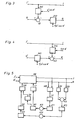
- Figure 1 is a block diagram over the portion of the radar receiver containing.the quadrature detector, correction unit and a regulating network in accordance with the invention
- FIG. 1 is a block diagram containing the units most closely associat- ed with the arrangement in accordance with the invention.
- a received radar signal appears across the input of the intermediate frequency amplifier MF following after the radar system circulator and mixer (not shown), which are conventionaLLy connected to the radar antenna.
- the quadrature detector which, as is known, contains a first phase detector FD1 in one channel and a second phase detector in the other channel.
- the signal to both phase detectors FD1, FD2 is, for example, a sinusoidal signal S cos ⁇ 2 ⁇ (f MF + f d ) t + ⁇ , where f MF is a reference frequency generated in the receiver, f d is the Doppler frequency and ⁇ an unknown (and variable) phase difference between the reference and received signals.
- a phase shift unit FS is connected to the phase detector FD2, to shift the phase of the reference signal cos 2 ⁇ (f MF t) applied to the detector FD2 by 90°, while the phase detector FD1 receives the reference signal cos 2 ⁇ f MF t without phase shift.
- Phase detection in relation to the reference signal (cos f MF t) thus takes place in the detectors FD1, FD2, and a bipolar video signal with a frequency equal to the Doppler displacement f d is obtained across the outputs of I' and Q'.
- the analogue-digital converters AD1, AD2 are connected to the phase detectors FD1 and FD2 in the respective channel for converting the detected analogue signals to digital signals with a suitable sampling frequency f .
- a correction unit KE is connected to both channels I' and Q', and will be described in detail in conjunction with Figures 3 and 4.
- the unit KE needs given correction signals for the correction, and these signals are formed by means of a regulating circuit RN with two separate input pairs, of which each terminal is connected to.the respective channel I and Q, which together constitute both outputs of the correction unit KE.
- the regulating network RN will be described beLow in conjunction with the description of Figures 6 and 7.
- phase and amplitude errors between the quadrature channels I' and Q' result in that a signal can be represented in an oblique coordinate system I', Q' according to Figure 2, where the quotient between the absolute values of the unit vectors is:
- Figures 3 and 4 are block diagrams over two alternative modes of realising the above relationships as far as hardware is concerned.
- Each of the Figures 3 and 4 corresponds to the correction unit KE of Figure 1.
- a multiplier M1 is connected across both channels I' and Q' via an addition circuit A1 and a multiplier M2 to the output of the addition circuit A1 in the Q' channel.
- a multiplier M3 is connected to the Q' crannel and a multiplier M4 between both channels via one input of an addition circuit A2, the other input of which is connected to the output of the multiplier M3.
- the output signal from the intermediate frequency amplifier MF is S(t) and is equal to:
- the output signal from the phase detector FD1, i e the component in the I' direction is S I' (t) MF and is equal to:
- the output signal from the phase detector FD2, i e the component in the Q' direction is S Q' (t) MF and is equal to: where a' and ⁇ ' are the amplitude and phase errors occurring in the detector FD2.
- phase error ⁇ ' can thus be determined by muLtipLication of both signals in the I' and Q' channels and subsequent summation.
- the summation time should be selected such that it is much Longer than the illumination time of an individual spot target.
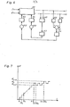
- Figure 5 illustrates an embodiment of the regulating network RN according to Figure 1 for determining the phase and amplitude errors ⁇ ' and a'.
- the network according to Figure 5 is constituted in principle of two loops. Both Loops are connected to the output of the correction unit KE for sensing the output signals S I and S Q across each channel.
- One loop contains a multiplier M5 and a summator S1, e g a feedback accumulator register for multiplying and summing both signals S I , and S QI according to the relationship above.
- a comparator circuit JF1 is connected to the output of the summator S1, and this comparator circuit compares the output signal from the summator S1 with a zero value. If the output signal is > 0 the comparator gives a binary value 1 across its output, and if the output signal is ⁇ 0, a binary value -1 is given across the output.
- the unit K11 connected to the output of the comparator JF1 is a multiplier which multiplies the value from the comparator by a suitable scale factor.
- the result is stored in a register R1 connected to the output of the unit K11, and corresponds to the value of sin ⁇ '.
- a calculating unit T1 is connected to the register R1 for calculating the value tan ⁇ ' from the value of ⁇ ' obtained from the register R1.
- the unit T1 can be an addresssable ROM memory in which the tangent values for a plurality of sin6' values are recorded in table form.
- the output signal from the unit T1, which thus corresponds to tan ⁇ ', is then supplied to the multiplier M4 in the block diagram according to Figure 4.
- the units M5, S1, JF1, K11, R1 and T1 described above are thus connected to the correction unit so that a regulating loop is formed for controlLing the value of sine tbwards zero.
- the factor a' can be calculated from the relationship:
- This regulating loop contains two absolute value-forming circuits B1 and B2, connected to both channels I and Q for sensing the signals S I and S Q .
- the outputs of the circuits B1 and B2 are connected to a plus and a minus input of an adding circuit A3, the output of which is connected to a comparator circuit JF2.
- the latter compares the difference
- the value across the output of the comparator JF2 is fed via a multiplier K12 to a register R2, the content of which represents the value of the quantity a'.
- An inverting circuit D2 is connected to the output of the register R2 to form a value 1/a', which is supplied to one input of a muLtipLier M6.
- the second input of the multiplier M6 is connected via an inverting circuit D1 to a second input of the register R1 in the regulating loop for the phase error ⁇ '.
- Signals representing the values 1/a' and a/cos ⁇ ' thus appear across both inputs of the multiplier M6, and across the output thereof is obtained a signal representing the value 1/a' cos ⁇ '.
- This value is applied to the multiplier M2 in Figure 3, or the multiplier M3 in Figure 4.
- the output signal of the summator S1 is Limited so that only its polarity is sensed by the subsequent comparator circuit JF1.
- the comparator circuit JF2 only senses the alteration in polarity of the error ⁇ a, cf relationship (3) above.
- the regulating network according to Figures 5 and 6 gives correction signals to the correction unit KE in Figure 4, but can be simply modified so that correction signals suited to the unit in Figure 3 are delivered.
- an inverter is con- rected to the output of the 1/a' register R3, followed by a multiplier with one input connected to the inverter and its other input connected to the output of the ⁇ -register R4. Across the multiplier output a signal is obtained corresponding to the value ⁇ ' ⁇ a' to the multiplier M1 according to Figure 3.
- Figure 7 is a time diagram illustrating the contents of the register R4 in Figure 6, i e the ⁇ ' register after a given number of sensed sampling i-tervals of the signals S and S Q on the I and Q channels.
- the regulating process for the phase and amplitude errors can require a somewhat longer time for coming to a steady state than if the test signal in accordance with known technology is used. This is no problem, however, since the only dynamic changes in the regulating circuit-depend on temperature drift in the phase detectors and video amplifier, these changes having a long time constant.
Abstract
Description
- The present invention relates to an arrangement, in accordance with the preamble of
claim 1, incorporated in a coherent Doppler radar system for correction of the errors in amplitude and phase of the received signal, occurring in the quadrature detector of the system. - In a Doppler radar system, the Doppler frequency of a target is determined by illuminating the target with a send signal, the echo of which is received and its signal processed in the receiver of the system. Before this signal processing in the MTI processor of the receiver, the target echo signal is taken through a quadrature detector, in which phase detection of the received signal is performed against two orthogonal components. The purpose of this division is to form a correct envelope signal for the detection at the final determination of the Doppler frequency. The division takes place in two channels, a so-called I channel ("in phase") and a so-called Q channel ("quadrature"), the output signals from the phase detectors arranged in the respective channel being processed individually before the final absolute value formation.
- The above-mentioned division into I and Q channels by means of two phase detectors has been known for a long time, and consequentLy the problems thus occurring are also known. Due to imperfections in both phase detectors as well as imperfections in the unit which phase-shifts the reference signal to the phase detector 90o in the Q channel, two components which are exactly orthogonal are not obtained in the received signal. This gives a phase error in the signal obtained from the detectors. Further, the attenuation in both detectors is not exactly alike, resulting in that the component in one channel is attenuated more or less than the component in the other channel, i e an amplitude error is obtained in the subsequent signal of which the envelope is detected.
- A number of previously known means have been proposed to remedy the above-mentioned imperfections of the quadrature detector. The earliest known method of improving accuracy was carefully to tune the detector to the best possible phase and amplitude likeness. New signal processing functions have substantially higher demands, which make tuning insufficient.
- The US Patent specifications 3.950.750, 4.003.054 and 4.122.448 iLLustrate systems in which special test signals are periodically connected to the quadrature detector. According to the specification 3.950.750, the output signal from the quadrature detector constituting the reply to the incoming test signal is analysed, and from the analysed output signal is derived.a plurality of correction coefficients which are supplied to the signals obtained when the radar illuminates an actual target.
- In previously known systems, a test signal is introduced into the system quadrature detector, and correction signals are formed from the response of the test signal for acting on the output signals from the detector, so that the error becomes zero. In accordance with the present invention, the first step-is to use an actual radar signal obtained from the antenna, this signal being applied to a correction unit after phase detection and analogue-digital conversion. The signals across the respective channels (I and Q) are applied to a correction unit connected to the analogue-digital converter in the respective channel, and the correction unit corrects these signals in the respective channels with respect to correct amplitude and phase. The correction is executed in response to correction signals from a regulating network, which senses the output signals from the correction links and controls the units in the correction links so that said errors become zero. The arrangement is thereby characterized by what can be read from the characterizing clause of
claim 1. - The object of the present invention is thus to provide an arrangement for eliminating the amplitude and phase errors occurring in a quadrature detector incorporated in the receiver of a Doppler radar system, by utilizing a correction link and a regulating network associated therewith for controLLing the link such that the errors become zero.
- An advantage with the arrangement is that the normal ordinary signals in the radar receiver can be utilized, a special test signal thus not being necessary.
- The invention will now be described more fuLLy while referring to the appended drawings, on which Figure 1 is a block diagram over the portion of the radar receiver containing.the quadrature detector, correction unit and a regulating network in accordance with the invention;
- Figure 2 shows an oblique coordinate system for illustrating the errors occurring in the quadrature detector of Figure 1;
- Figures 3 and 4 are block diagrams of two embodiments of the correction unit according in Figure 1;
- Figure 5 is a block diagram of an embodiment of the regulating network in Figure 1;
- Figure 6 illustrates a simplified embodiment of the regulating network in Figure 5;
- Figure 7 is a time diagram for more closely iLLustrating the function of the regulating network according to Figure 6.
- Figure 1 is a block diagram containing the units most closely associat- ed with the arrangement in accordance with the invention. A received radar signal appears across the input of the intermediate frequency amplifier MF following after the radar system circulator and mixer (not shown), which are conventionaLLy connected to the radar antenna. After the intermediate frequency amplifier MF there comes the quadrature detector, which, as is known, contains a first phase detector FD1 in one channel and a second phase detector in the other channel. In a Doppler radar system, the signal to both phase detectors FD1, FD2 is, for example, a sinusoidal signal S cos{2π(fMF+ fd) t + φ}, where f MF is a reference frequency generated in the receiver, fd is the Doppler frequency and φ an unknown (and variable) phase difference between the reference and received signals.
- A phase shift unit FS is connected to the phase detector FD2, to shift the phase of the reference signal cos 2π (fMFt) applied to the detector FD2 by 90°, while the phase detector FD1 receives the reference signal cos 2π fMFt without phase shift. Phase detection in relation to the reference signal (cos fMFt) thus takes place in the detectors FD1, FD2, and a bipolar video signal with a frequency equal to the Doppler displacement fd is obtained across the outputs of I' and Q'.
- The analogue-digital converters AD1, AD2 are connected to the phase detectors FD1 and FD2 in the respective channel for converting the detected analogue signals to digital signals with a suitable sampling frequency f .
- Due to imperfections in the units FD1, FD2 and FS, no exact phase de- tection against two orthogonal signals (i e cos 2π fMFt and cos 2π fMFt + π/2) can be achieved. The signals occurring in the channels I' and Q' are thus burdened with a certain error in amplitude and phase, which will be eliminated with the aid of the arrangement in accordance with the invention. For this purpose, a correction unit KE is connected to both channels I' and Q', and will be described in detail in conjunction with Figures 3 and 4. The unit KE needs given correction signals for the correction, and these signals are formed by means of a regulating circuit RN with two separate input pairs, of which each terminal is connected to.the respective channel I and Q, which together constitute both outputs of the correction unit KE. The regulating network RN will be described beLow in conjunction with the description of Figures 6 and 7.
- The phase and amplitude errors between the quadrature channels I' and Q' result in that a signal can be represented in an oblique coordinate system I', Q' according to Figure 2, where the quotient between the absolute values of the unit vectors is:

- If a' and the phase error θ' are known, a conversion calculation can be made to obtain a correct right-angular coordinate system I, Q with a=1 and θ = 0. The foLLowing relationships apply:


- To carry this out in an apparatus, rapid digital multipliers and addition circuits are used, for example. Figures 3 and 4 are block diagrams over two alternative modes of realising the above relationships as far as hardware is concerned..Each of the Figures 3 and 4 corresponds to the correction unit KE of Figure 1.
- In Figure 3, a multiplier M1 is connected across both channels I' and Q' via an addition circuit A1 and a multiplier M2 to the output of the addition circuit A1 in the Q' channel. In Figure 4, a multiplier M3 is connected to the Q' crannel and a multiplier M4 between both channels via one input of an addition circuit A2, the other input of which is connected to the output of the multiplier M3.
- So that the correction unit KE can correct the signals coming in across the channels I' and Q', signals must be formed which correspond to the input signals a' sine' and 1/a' coset in the embodiment according to Figure 3, or input signals corresponding to 1/a' cos θ' and tanθ' in the embodiment according to Figure 4. This is provided by the regulating network RN in Figure 1.
- There is always some form of signal across both outputs of the quadrature detector (after analogue - digital conversion). This signal can either come from thermic noise in the input stage (mixer and amplifier) of the signal receiver, or from echo signals captured by the receiver antenna. Assume that such a signal S(t) has the components SI, (t) and SQ'(t) in the respective channels I' and Q'. The phase error θ' is then obtained from the relationship:

- This relationship can be derived in the following manner:
- The output signal from the intermediate frequency amplifier MF is S(t) and is equal to:

- The output signal from the phase detector FD1, i e the component in the I' direction is SI'(t)MF and is equal to:


- The output signal from the phase detector FD2, i e the component in the Q' direction is SQ' (t)MF and is equal to:

-


- This relationship is valid for an individual signal sample after the analogue-digital converters AD1, AD2. The product SI' - SQ' is summed for a long period, i e for a Large number of independent sample values. The Doppler frequency fd and the distance - dependent phase angle φ are correlated for different samples coming from the same target, but vary randomly between different targets.
- If the summation time is made very much larger than the illumination time of an individual target, the result will not be affected by this correlation. In summation over a large number of samples, the contributions from the first and last term in (c) wilt be zero. The same thing applies to the terms sin (θ'-2 ) and sin(2φ-θ'). The sum of the product SI' - SQ, for N signal samples will then be:

- The value of the phase error θ' can thus be determined by muLtipLication of both signals in the I' and Q' channels and subsequent summation. In a practical application, the summation time should be selected such that it is much Longer than the illumination time of an individual spot target.
- Figure 5 illustrates an embodiment of the regulating network RN according to Figure 1 for determining the phase and amplitude errors θ' and a'. The network according to Figure 5 is constituted in principle of two loops. Both Loops are connected to the output of the correction unit KE for sensing the output signals SI and SQ across each channel.
- One loop contains a multiplier M5 and a summator S1, e g a feedback accumulator register for multiplying and summing both signals SI, and SQI according to the relationship above. A comparator circuit JF1 is connected to the output of the summator S1, and this comparator circuit compares the output signal from the summator S1 with a zero value. If the output signal is > 0 the comparator gives a
binary value 1 across its output, and if the output signal is < 0, a binary value -1 is given across the output. The unit K11 connected to the output of the comparator JF1 is a multiplier which multiplies the value from the comparator by a suitable scale factor. The result is stored in a register R1 connected to the output of the unit K11, and corresponds to the value of sin θ'. A calculating unit T1 is connected to the register R1 for calculating the value tanθ' from the value of θ' obtained from the register R1. The unit T1 can be an adressable ROM memory in which the tangent values for a plurality of sin6' values are recorded in table form. The output signal from the unit T1, which thus corresponds to tanθ', is then supplied to the multiplier M4 in the block diagram according to Figure 4. - The units M5, S1, JF1, K11, R1 and T1 described above are thus connected to the correction unit so that a regulating loop is formed for controlLing the value of sine tbwards zero.
- Providing that the input signal to the quadrature detector has a rectan- gular phase distribution and that no correlation between phase and amplitude is present, the factor a' can be calculated from the relationship:

- Further, a factor

- According to Figure 5, a regulating loop is also arranged for the amplitude error to control the error Δa towards zero, i e a=1. This regulating loop contains two absolute value-forming circuits B1 and B2, connected to both channels I and Q for sensing the signals SI and SQ. The outputs of the circuits B1 and B2 are connected to a plus and a minus input of an adding circuit A3, the output of which is connected to a comparator circuit JF2. The latter compares the difference |SQ| - |SI| with the value zero, and if the difference is greater than zero, +1 is obtained across the output, otherwise -1. The value across the output of the comparator JF2 is fed via a multiplier K12 to a register R2, the content of which represents the value of the quantity a'. An inverting circuit D2 is connected to the output of the register R2 to form a
value 1/a', which is supplied to one input of a muLtipLier M6. The second input of the multiplier M6 is connected via an inverting circuit D1 to a second input of the register R1 in the regulating loop for the phase error θ'. Signals representing thevalues 1/a' and a/cosθ' thus appear across both inputs of the multiplier M6, and across the output thereof is obtained a signal representing thevalue 1/a' cosθ'. This value is applied to the multiplier M2 in Figure 3, or the multiplier M3 in Figure 4. - To avoid the signal amplitude due to the factor a' · s-2 i (1) above affecting the regulating network feedback amplification, the output signal of the summator S1 is Limited so that only its polarity is sensed by the subsequent comparator circuit JF1. In a corresponding manner the comparator circuit JF2 only senses the alteration in polarity of the error Δa, cf relationship (3) above.
- Certain simplifications in respect of apparatus can be done by putting tan6' =6' and cosθ' =1. The error thus introduced will automatically be compensated by the regulating network RN. The register R2 in Figure 5 can furthermore be replaced by a register (the b register) which stores a value b=1/a', in which case the polarity of the input signal to the register must be changed.
- It is furthermore obvious that if the register R1 (the θ' register), can be updated at an equally high rate as the input signal rate to the multiplier M5 in Figure 5, the summator S1 can be eliminated and the integration sequence is carried out in the register R1 on the signal obtained from the I and Q channels and processed in the multiplier M5 and comparator circuit JF1. The block diagram of Figure 5 can thus be simplified to the block diagram of Figure 6, the Latter iLLustrating the preferred embodiment. Two entirely separate regulating loops are arranged in Figure 6 for the phase and amplitud errors θ' and a'. In the regulating loop for the phase error, a comparison of the product value SI, SQ, obtained in the multiplier M7 is made in respect of the polarity of this product, and the summation is carried out in the register R4 after multiplying by a suitable scale factor in the multiplier K21. The unit T1 in Figure 5 has been dispensed with, since tanθ' has been approximated to 6'. In the regulating loop for the amplitude error, the register R2 has been replaced by a register R3 for storing 1/a', and the multiplier M6 has been dispensed with, since cosθ' has been approximated to 1.
- The regulating network according to Figures 5 and 6 gives correction signals to the correction unit KE in Figure 4, but can be simply modified so that correction signals suited to the unit in Figure 3 are delivered. In the block diagram according to Figure 6, an inverter is con- rected to the output of the 1/a' register R3, followed by a multiplier with one input connected to the inverter and its other input connected to the output of the θ-register R4. Across the multiplier output a signal is obtained corresponding to the value θ' · a' to the multiplier M1 according to Figure 3.
- Figure 7 is a time diagram illustrating the contents of the register R4 in Figure 6, i e the θ' register after a given number of sensed sampling i-tervals of the signals S and SQ on the I and Q channels. After n sensed signal samples, i e at the time n · t s where ts = 1/fs (the samp- ting interval) the value of θ' =θ'n is such that the correction unit KE has corrected the signals SI, and SQ', such that these are as close as possible orthogonal with regard to the quantizing, and the comparator circuit JF3 delivers +1. Upon the next sensing, at t= (n+1)ts, θ' =θ'n+1, and the comparator JF3 delivers -1. The values θ'n and θ'n+1 represent t-e constant error substantially to be found in the quadrature detector F:1, FD2, FS at the time n · t . At the instant (n+k)t a change occurs in the quadrature detector, e g due to temperature variations, and the regulating Loop for the phase error θ' reacts by increasing the value of 6' to a new value θ'n+k, regulation according to the preceding then being carried out.
- The regulating process for the phase and amplitude errors can require a somewhat longer time for coming to a steady state than if the test signal in accordance with known technology is used. This is no problem, however, since the only dynamic changes in the regulating circuit-depend on temperature drift in the phase detectors and video amplifier, these changes having a long time constant.
Claims (4)
characterized by a regulating network (RN) for forming the first and the second correction signal, said network containing two regulating loops, of which
Applications Claiming Priority (2)
| Application Number | Priority Date | Filing Date | Title |
|---|---|---|---|
| SE8006396 | 1980-09-12 | ||
| SE8006396A SE419581B (en) | 1980-09-12 | 1980-09-12 | DEVICE IN A RADAR SYSTEM FOR CORRECTION OF PHASE AND AMPLIT ERRORS WHICH APPEAR IN THE SQUARE DETECTOR |
Publications (3)
| Publication Number | Publication Date |
|---|---|
| EP0048229A2 true EP0048229A2 (en) | 1982-03-24 |
| EP0048229A3 EP0048229A3 (en) | 1982-07-07 |
| EP0048229B1 EP0048229B1 (en) | 1984-10-10 |
Family
ID=20341719
Family Applications (1)
| Application Number | Title | Priority Date | Filing Date |
|---|---|---|---|
| EP81850147A Expired EP0048229B1 (en) | 1980-09-12 | 1981-09-04 | Arrangement in a radar system for correction of phase and amplitude errors in a video signal |
Country Status (4)
| Country | Link |
|---|---|
| US (1) | US4484194A (en) |
| EP (1) | EP0048229B1 (en) |
| DE (1) | DE3166625D1 (en) |
| SE (1) | SE419581B (en) |
Cited By (9)
| Publication number | Priority date | Publication date | Assignee | Title |
|---|---|---|---|---|
| EP0180339A2 (en) * | 1984-10-25 | 1986-05-07 | Stc Plc | A multi-mode radio transceiver |
| EP0204570A2 (en) * | 1985-06-06 | 1986-12-10 | THE GENERAL ELECTRIC COMPANY, p.l.c. | Digital mixing apparatus |
| EP0271266A2 (en) * | 1986-12-09 | 1988-06-15 | Nortel Networks Corporation | Signal processing |
| EP0343273A1 (en) * | 1988-05-27 | 1989-11-29 | Deutsche ITT Industries GmbH | Correction circuit for a pair of digital quadrature signals |
| DE3938643A1 (en) * | 1988-11-22 | 1990-05-23 | Ascom Radiocom Ag | Reconstructing lost DC components of IF signals - applying correction signal to each fault-laden IF signal and generating corrected signal |
| EP0401771A2 (en) * | 1989-06-09 | 1990-12-12 | TEMIC TELEFUNKEN microelectronic GmbH | Circuit arrangement for frequency conversion |
| EP0429090A2 (en) * | 1989-11-24 | 1991-05-29 | SELENIA INDUSTRIE ELETTRONICHE ASSOCIATE S.p.A. | Device for the automatic correction of the differential error, preferably for a monopulse radar receiver |
| EP0490275A2 (en) * | 1990-12-10 | 1992-06-17 | Hughes Aircraft Company | System and method for compensation of in-phase and quadrature phase and gain imbalance |
| EP0647031A1 (en) * | 1993-10-05 | 1995-04-05 | Eta SA Fabriques d'Ebauches | Circuit for correcting phase-shift and amplitudes |
Families Citing this family (20)
| Publication number | Priority date | Publication date | Assignee | Title |
|---|---|---|---|---|
| US4532516A (en) * | 1982-10-18 | 1985-07-30 | The Singer Company | Calibrator for distance measuring equipment |
| US4800387A (en) * | 1984-02-07 | 1989-01-24 | Logimetrics, Inc. | Boresight chamber assembly apparatus |
| US4812849A (en) * | 1984-09-17 | 1989-03-14 | General Dynamics Corporation | Nonquadrature correction circuit |
| US4768035A (en) * | 1985-04-18 | 1988-08-30 | The Johns Hopkins University | Coherent radar digital data collector and sampling technique for noncoherent transmitter radars |
| US5027127A (en) * | 1985-10-10 | 1991-06-25 | United Technologies Corporation | Phase alignment of electronically scanned antenna arrays |
| US4783660A (en) * | 1986-09-29 | 1988-11-08 | Signatron, Inc. | Signal source distortion compensator |
| US4940985A (en) * | 1988-11-02 | 1990-07-10 | Westinghouse Electric Corp. | Radar stability measurement system |
| US4994810A (en) * | 1990-03-26 | 1991-02-19 | Allied-Signal Inc. | Monopulse processor digital correction circuit |
| US5036333A (en) * | 1990-06-21 | 1991-07-30 | Hughes Aircraft Company | Antenna-rotation compensation apparatus and method for phased array antennas |
| US5872538A (en) * | 1998-02-26 | 1999-02-16 | Lockheed Martin Corporation | Frequency domain correction of I/Q imbalance |
| GB2349285B (en) * | 1999-04-19 | 2003-02-12 | Oak Technology Inc | Signal correction |
| US7088765B1 (en) * | 2000-03-15 | 2006-08-08 | Ndsu Research Foundation | Vector calibration system |
| DE102004047424A1 (en) * | 2004-09-28 | 2006-04-06 | Micronas Gmbh | Circuit and method for carrier recovery |
| DE102004048572A1 (en) * | 2004-10-04 | 2006-04-13 | Micronas Gmbh | Method and circuit arrangement for suppressing an orthogonal disturbance |
| DE102004054893A1 (en) * | 2004-11-12 | 2006-05-24 | Micronas Gmbh | Method and circuit arrangement for channel filtering analog or digitally modulated TV signals |
| US7830991B2 (en) * | 2005-10-03 | 2010-11-09 | Harris Corporation | Frequency selective automatic gain control with dual non-symmetric attack and release times and interference detection feature |
| US7170440B1 (en) * | 2005-12-10 | 2007-01-30 | Landray Technology, Inc. | Linear FM radar |
| CN101272522B (en) * | 2007-03-20 | 2010-10-27 | 大唐移动通信设备有限公司 | Method, system and base station for single frequency network transmitting multimedia broadcast/multicast service |
| US9448301B2 (en) | 2013-12-20 | 2016-09-20 | Delta Mobile Systems, Inc. | Calibrated radar apparatus and associated methods |
| US9684070B2 (en) | 2013-12-20 | 2017-06-20 | Delta Mobile Systems, Inc | Radar apparatus with quiet switch calibration and associated methods |
Citations (5)
| Publication number | Priority date | Publication date | Assignee | Title |
|---|---|---|---|---|
| US2201193A (en) * | 1936-03-26 | 1940-05-21 | Roy F Mcmahan | Method of attaching a hanger |
| US3675129A (en) * | 1970-05-13 | 1972-07-04 | Collins Radio Co | Differentially coherent phase shift keyed digital demodulating apparatus |
| US3742500A (en) * | 1970-08-24 | 1973-06-26 | Raytheon Co | Mti radar |
| US3950750A (en) * | 1974-10-03 | 1976-04-13 | Raytheon Company | Radar system having quadrature phase detector compensator |
| US4122448A (en) * | 1977-07-21 | 1978-10-24 | Westinghouse Electric Corp. | Automatic phase and gain balance controller for a baseband processor |
Family Cites Families (7)
| Publication number | Priority date | Publication date | Assignee | Title |
|---|---|---|---|---|
| US3794998A (en) * | 1972-04-26 | 1974-02-26 | Raytheon Co | Monopulse radar receiver with error correction |
| US3883870A (en) * | 1973-12-17 | 1975-05-13 | Hughes Aircraft Co | System for phase aligning parallel signal processing channels |
| US4003054A (en) * | 1974-10-03 | 1977-01-11 | Raytheon Company | Method of compensating for imbalances in a quadrature demodulator |
| US4083015A (en) * | 1976-04-21 | 1978-04-04 | Westinghouse Electric Corporation | Fast switching phase lock loop system |
| US4093949A (en) * | 1976-05-26 | 1978-06-06 | Hughes Aircraft Company | Clutter tracker using a smoothed doppler frequency measurement |
| US4079329A (en) * | 1976-11-11 | 1978-03-14 | Harris Corporation | Signal demodulator including data normalization |
| US4132990A (en) * | 1977-10-12 | 1979-01-02 | United Technologies Corporation | Amti target/clutter discriminator |
-
1980
- 1980-09-12 SE SE8006396A patent/SE419581B/en not_active IP Right Cessation
-
1981
- 1981-08-31 US US06/297,836 patent/US4484194A/en not_active Expired - Lifetime
- 1981-09-04 EP EP81850147A patent/EP0048229B1/en not_active Expired
- 1981-09-04 DE DE8181850147T patent/DE3166625D1/en not_active Expired
Patent Citations (5)
| Publication number | Priority date | Publication date | Assignee | Title |
|---|---|---|---|---|
| US2201193A (en) * | 1936-03-26 | 1940-05-21 | Roy F Mcmahan | Method of attaching a hanger |
| US3675129A (en) * | 1970-05-13 | 1972-07-04 | Collins Radio Co | Differentially coherent phase shift keyed digital demodulating apparatus |
| US3742500A (en) * | 1970-08-24 | 1973-06-26 | Raytheon Co | Mti radar |
| US3950750A (en) * | 1974-10-03 | 1976-04-13 | Raytheon Company | Radar system having quadrature phase detector compensator |
| US4122448A (en) * | 1977-07-21 | 1978-10-24 | Westinghouse Electric Corp. | Automatic phase and gain balance controller for a baseband processor |
Cited By (21)
| Publication number | Priority date | Publication date | Assignee | Title |
|---|---|---|---|---|
| EP0180339A2 (en) * | 1984-10-25 | 1986-05-07 | Stc Plc | A multi-mode radio transceiver |
| EP0180339A3 (en) * | 1984-10-25 | 1988-01-07 | Stc Plc | A multi-mode radio transceiver |
| EP0204570A2 (en) * | 1985-06-06 | 1986-12-10 | THE GENERAL ELECTRIC COMPANY, p.l.c. | Digital mixing apparatus |
| EP0204570A3 (en) * | 1985-06-06 | 1988-12-07 | THE GENERAL ELECTRIC COMPANY, p.l.c. | Digital mixing apparatus |
| EP0271266A2 (en) * | 1986-12-09 | 1988-06-15 | Nortel Networks Corporation | Signal processing |
| EP0271266A3 (en) * | 1986-12-09 | 1989-12-13 | Stc Plc | Signal processing |
| EP0343273A1 (en) * | 1988-05-27 | 1989-11-29 | Deutsche ITT Industries GmbH | Correction circuit for a pair of digital quadrature signals |
| US4926443A (en) * | 1988-05-27 | 1990-05-15 | Deutsche Itt Industries Gmbh | Correction circuit for a digital quadrature-signal pair |
| DE3938643A1 (en) * | 1988-11-22 | 1990-05-23 | Ascom Radiocom Ag | Reconstructing lost DC components of IF signals - applying correction signal to each fault-laden IF signal and generating corrected signal |
| DE3938643C2 (en) * | 1988-11-22 | 1999-03-25 | Motorola Inc | Method for reconstructing separated direct-current useful components of IF signals in a direct conversion receiver and receiver for carrying out the method |
| US5179731A (en) * | 1989-06-09 | 1993-01-12 | Licentia-Patent-Verwaltungs-Gmbh | Frequency conversion circuit |
| EP0401771A3 (en) * | 1989-06-09 | 1991-09-04 | TEMIC TELEFUNKEN microelectronic GmbH | Circuit arrangement for frequency conversion |
| EP0401771A2 (en) * | 1989-06-09 | 1990-12-12 | TEMIC TELEFUNKEN microelectronic GmbH | Circuit arrangement for frequency conversion |
| EP0429090A3 (en) * | 1989-11-24 | 1991-12-04 | Selenia Industrie Elettroniche Associate S.P.A. | Device for the automatic correction of the differential error, preferably for a monopulse radar receiver |
| EP0429090A2 (en) * | 1989-11-24 | 1991-05-29 | SELENIA INDUSTRIE ELETTRONICHE ASSOCIATE S.p.A. | Device for the automatic correction of the differential error, preferably for a monopulse radar receiver |
| EP0490275A2 (en) * | 1990-12-10 | 1992-06-17 | Hughes Aircraft Company | System and method for compensation of in-phase and quadrature phase and gain imbalance |
| EP0490275A3 (en) * | 1990-12-10 | 1992-08-05 | Hughes Aircraft Company | System and method for compensation of in-phase and quadrature phase and gain imbalance |
| TR26255A (en) * | 1990-12-10 | 1995-02-15 | Hughes Aircraft Co | SYSTEM AND METHOD FOR IMPROVING PHASE ADJUSTMENT AND 90-DEGREE PHASE DIFFERENCE AND GAIN UNBALANCE |
| EP0647031A1 (en) * | 1993-10-05 | 1995-04-05 | Eta SA Fabriques d'Ebauches | Circuit for correcting phase-shift and amplitudes |
| FR2711027A1 (en) * | 1993-10-05 | 1995-04-14 | Ebauchesfabrik Eta Ag | Phase shift and amplitude correction circuit. |
| US5635876A (en) * | 1993-10-05 | 1997-06-03 | Eta Sa Fabriques D'ebauches | Phase difference and amplitude correction circuit |
Also Published As
| Publication number | Publication date |
|---|---|
| DE3166625D1 (en) | 1984-11-15 |
| EP0048229B1 (en) | 1984-10-10 |
| EP0048229A3 (en) | 1982-07-07 |
| SE419581B (en) | 1981-08-10 |
| US4484194A (en) | 1984-11-20 |
Similar Documents
| Publication | Publication Date | Title |
|---|---|---|
| EP0048229B1 (en) | Arrangement in a radar system for correction of phase and amplitude errors in a video signal | |
| US5105195A (en) | System and method for compensation of in-phase and quadrature phase and gain imbalance | |
| US4003054A (en) | Method of compensating for imbalances in a quadrature demodulator | |
| US4475088A (en) | Gain imbalance corrected quadrature phase detector | |
| US4675614A (en) | Phase difference measurement system | |
| US3950750A (en) | Radar system having quadrature phase detector compensator | |
| US5150128A (en) | In-phase and quadrature conversion error compensator | |
| EP0360770B1 (en) | Log-polar signal processing | |
| US4528565A (en) | Pulse doppler radar receiver with a circuit for reducing spurious signals | |
| US5477230A (en) | AOA application of digital channelized IFM receiver | |
| US4584710A (en) | Coherent receiver phase and amplitude alignment circuit | |
| US4231005A (en) | Constant false alarm rate radar system and method of operating the same | |
| US5184135A (en) | Phase measurement of received pseudonoise sequence using digital correlation | |
| US5619206A (en) | Secondary radar digital monopulse receiving apparatus and method | |
| CZ279597A3 (en) | Receiver | |
| US3953805A (en) | DC component suppression in zero CF IF systems | |
| US4170006A (en) | Radar speed measurement from range determined by focus | |
| US4220953A (en) | Circuit arrangement for improving accuracy of angular measurements in radar systems | |
| US5315620A (en) | Arrangement for correction of synchronous demodulator quadrature phase errors | |
| US4926184A (en) | Angle measurement device for amplitude monopulse receivers | |
| JPH0146835B2 (en) | ||
| US5559517A (en) | Maximized/minimized phase calculator for an interferometric amti radar | |
| US4163975A (en) | Method of measuring the altitude of a target maneuvering at a very low elevation, and a tracking radar using same | |
| US3218559A (en) | Synchronizing circuit maintaining loop signals as an integer product and equal amplitude | |
| US5848099A (en) | Method and system for testing phase imbalance in QPSK receivers |
Legal Events
| Date | Code | Title | Description |
|---|---|---|---|
| PUAI | Public reference made under article 153(3) epc to a published international application that has entered the european phase |
Free format text: ORIGINAL CODE: 0009012 |
|
| AK | Designated contracting states |
Designated state(s): CH DE FR GB IT NL |
|
| PUAL | Search report despatched |
Free format text: ORIGINAL CODE: 0009013 |
|
| RHK1 | Main classification (correction) |
Ipc: G01S 13/52 |
|
| AK | Designated contracting states |
Designated state(s): CH DE FR GB IT NL |
|
| 17P | Request for examination filed |
Effective date: 19820818 |
|
| ITF | It: translation for a ep patent filed |
Owner name: FUMERO BREVETTI S.N.C. |
|
| GRAA | (expected) grant |
Free format text: ORIGINAL CODE: 0009210 |
|
| AK | Designated contracting states |
Designated state(s): CH DE FR GB IT LI NL |
|
| REF | Corresponds to: |
Ref document number: 3166625 Country of ref document: DE Date of ref document: 19841115 |
|
| ET | Fr: translation filed | ||
| PLBE | No opposition filed within time limit |
Free format text: ORIGINAL CODE: 0009261 |
|
| STAA | Information on the status of an ep patent application or granted ep patent |
Free format text: STATUS: NO OPPOSITION FILED WITHIN TIME LIMIT |
|
| 26N | No opposition filed | ||
| ITTA | It: last paid annual fee | ||
| PGFP | Annual fee paid to national office [announced via postgrant information from national office to epo] |
Ref country code: GB Payment date: 19990820 Year of fee payment: 19 Ref country code: FR Payment date: 19990820 Year of fee payment: 19 Ref country code: DE Payment date: 19990820 Year of fee payment: 19 |
|
| PGFP | Annual fee paid to national office [announced via postgrant information from national office to epo] |
Ref country code: NL Payment date: 19990823 Year of fee payment: 19 |
|
| PGFP | Annual fee paid to national office [announced via postgrant information from national office to epo] |
Ref country code: CH Payment date: 19990906 Year of fee payment: 19 |
|
| PG25 | Lapsed in a contracting state [announced via postgrant information from national office to epo] |
Ref country code: GB Free format text: LAPSE BECAUSE OF NON-PAYMENT OF DUE FEES Effective date: 20000904 |
|
| PG25 | Lapsed in a contracting state [announced via postgrant information from national office to epo] |
Ref country code: LI Free format text: LAPSE BECAUSE OF NON-PAYMENT OF DUE FEES Effective date: 20000930 Ref country code: CH Free format text: LAPSE BECAUSE OF NON-PAYMENT OF DUE FEES Effective date: 20000930 |
|
| PG25 | Lapsed in a contracting state [announced via postgrant information from national office to epo] |
Ref country code: NL Free format text: LAPSE BECAUSE OF NON-PAYMENT OF DUE FEES Effective date: 20010401 |
|
| GBPC | Gb: european patent ceased through non-payment of renewal fee |
Effective date: 20000904 |
|
| REG | Reference to a national code |
Ref country code: CH Ref legal event code: PL |
|
| PG25 | Lapsed in a contracting state [announced via postgrant information from national office to epo] |
Ref country code: FR Free format text: LAPSE BECAUSE OF NON-PAYMENT OF DUE FEES Effective date: 20010531 |
|
| NLV4 | Nl: lapsed or anulled due to non-payment of the annual fee |
Effective date: 20010401 |
|
| PG25 | Lapsed in a contracting state [announced via postgrant information from national office to epo] |
Ref country code: DE Free format text: LAPSE BECAUSE OF NON-PAYMENT OF DUE FEES Effective date: 20010601 |
|
| REG | Reference to a national code |
Ref country code: FR Ref legal event code: ST |