EP0048557A1 - Electronic coin validators - Google Patents
Electronic coin validators Download PDFInfo
- Publication number
- EP0048557A1 EP0048557A1 EP81304000A EP81304000A EP0048557A1 EP 0048557 A1 EP0048557 A1 EP 0048557A1 EP 81304000 A EP81304000 A EP 81304000A EP 81304000 A EP81304000 A EP 81304000A EP 0048557 A1 EP0048557 A1 EP 0048557A1
- Authority
- EP
- European Patent Office
- Prior art keywords
- coin
- validator
- coil
- signal
- electronic coin
- Prior art date
- Legal status (The legal status is an assumption and is not a legal conclusion. Google has not performed a legal analysis and makes no representation as to the accuracy of the status listed.)
- Granted
Links
Images


Classifications
-
- G—PHYSICS
- G07—CHECKING-DEVICES
- G07D—HANDLING OF COINS OR VALUABLE PAPERS, e.g. TESTING, SORTING BY DENOMINATIONS, COUNTING, DISPENSING, CHANGING OR DEPOSITING
- G07D5/00—Testing specially adapted to determine the identity or genuineness of coins, e.g. for segregating coins which are unacceptable or alien to a currency
- G07D5/08—Testing the magnetic or electric properties
Definitions
- the present invention relates to electronic coin validators.
- a step change of magnetic flux is applied axially to a coin an eddy current is induced which flows in the periphery of the coin, the coin acts like a coil comprising a single shorted turn.
- the coin has an inductance Lc and an equivalent series resistance Rc, related to the resistivity of the coin and its resistance.
- the eddy current induced in the coin is also related to the current step I in the transmit coil that produces the step change of magnetic flux and the mutual coupling Me between the coil and coin.
- the current can be used to give an electronic signature that defines the coin type.
- an electronic coin validator including a transmit coil for creating a magnetic field, a receive coil for detecting changes in the magnetic field due to the presence of a coin adjacent to the coils, and means whereby tne validator operates to perform a test on the coin, to give a first parameter which is a measure of the coin face area, and a second parameter which is a measure of the coin resistance, said first and second parameters being used to establish the validity of tne coin.
- an electronic coin validator including a transmit coil for creating a magnetic field and a receive coil for detecting the transmitted magnetic field, said receive coil being used to detect a compensation signal when the transmit coil is activated, which signal is unaffected by the coin to be validated.
- the magnetic field is larger than the largest coin to be tested and two parameters are measured, coin face area and coin resistance.
- the receive coil current waveform is shown in Figure 2. If the open circuit voltage in the coin, is detected, the peak voltage is a measure of a coin face area and the integrated voltage waveform has a time constant related to the coin resistance.
- the circuit of Figure 1 produces the waveforms of Figure 2. It consists of a current switch CS which has a defined turn on time, and drives the transmit coil TC.
- the receive coil RC drives an amplifier which is connected to an integrator I and a peak detector PD.
- a comparator set at 90% of the integrator maximum output voltage gives a signal that allows t.coin to be measured, where t coin is the time taken for the integrator output voltage to rise to the 90% level.
- a start pulse gates a 10 MHz clock into a counter chain CC via flip flop FF1 when the transmit current step is applied, and, the integrator output stops the count.
- the number in the counter is now a measure of t coin which relates to coin resistance, and may be applied to a microprocessor ⁇ P for evaluation.
- the peak detector holds the peak impulse shown in Figure 2 and can produce the set of output voltages shown in Figure 3 for the different coins.
- the peak detector drives four window gates WG, one of which is shown, whose thresholds are adjusted to each coin face area distribution.
- the window comparator outputs are gated into a 'D' type flip-flop FF2 that are clocked 5 u S after the start of the coin test, this effectively produces a peak detector output sample at 5 ⁇ S, as shown in Figure 3.
- the output of each flip-flop FF2 may be applied to the microprocessorup for evaluation.
- the peak detector voltage may be entered into an analog-to-digital converter and the output applied to a microprocessor for evaluation.
- step T If the step is of rise time T, this is modified to:
- the voltage in the receive coil due to the presence of the coin is modified to: and this has to be added to the voltage due to the direct flux in order to give the complete receive waveform. It can be seen from the equations that if a test impulse is applied when no coin is present then this can be used to provide a reference level providing compensation for the effects of drift etc.
- the coin validator verifies two parameters of a coin before it is passed as genuine.
- Any disc of the correct size will meet the size parameter, but then has to have a time t coin inside the correct time distribution to meet the second parameter and be recognised as genuine.
- the validator uses identical transmit and receive coils wound on the outside of a ferrite vinkor..
- the area of the coil is quite critical and has to be such as to allow sufficient flux to pass around each coin and also produce an easily measurable t-coin period in excess of 10 uS.
- the multi-frequency validator carries out a test to verify two parameters of the coin.
- the first parameter is of face area of the coin, and the second parameter is of the coin resistance.
- a magnetic field larger than the largest coin face area is produced across the coin runway between the transmit and receive coils.
- the field can be either produced by an alternating current or a step change of current in the transmit coil.
- the multi-frequency validator has a transmit coil TC which is driven by a coil drive circuit CD.
- the coil drive circuit CD is fed with a multi-frequency signal generated from oscillator OSC and divider circuit DV via a signal amplitude control circuit AC, filter circuits F1-F4 and summing and amplitude weighting circuit SW.
- the receive coil RC drives a differential amplifier DA and filters F5-F8.
- the output of the filters is fed via respective rectifier circuits R1-R3 to detector circuits D1-D3 the outputs of which are selectively switched by switch S to analog-to-digital converter ADO to a microprocessor pP for evaluation.
- Rectifier R4 feeds an automatic gain control circuit AGO which also receives a voltage reference signal from circuit VR.
- the output of the automatic gain control circuit AGO is used to modify the operation of signal amplitude control circuit AC to compensate for temperature changes in inductance, drift etc.
- the graph shown in Figure 5 shows the normalized receive coil voltage NCV against transmit current frequency f. At frequencies below 1KHz the received signal amplitude is unaffected by the presence of the coin set of interest and so can be used for a continuous reference tone that compensates for variations in mutual inductance, temperature effects and component drift.
- the coin is opaque to the applied magnetic field and so the majority of the received signal is due to the field that gets round the edge of the coin, therefore the ratio of the amplitude of the received signal with and without the coin present gives a measure of the coin face area. If amplitude measurements are taken in the receive coil at two frequencies between 1KHz and 100KHz we can get a measure of the coin resistance.
- the open circuit receive coil voltage is:-
- a w cos wt gives a measure of coin face area at high frequency and the other terms at lower frequencies give a measure of coin resistance.
- Voc varies in amplitude with w and M.
- An accurately controlled frequency using a crystal master clock will prevent variations in w effecting Voc.
- coin face area is the ratio of the magnetic field passing round the coin to that when no coin is present and is directly proportional to the mechanical dimensions of the receive coil, which vary from coil to coil.
Abstract
Description
- The present invention relates to electronic coin validators. When a step change of magnetic flux is applied axially to a coin an eddy current is induced which flows in the periphery of the coin, the coin acts like a coil comprising a single shorted turn. The coin has an inductance Lc and an equivalent series resistance Rc, related to the resistivity of the coin and its resistance. The eddy current induced in the coin is also related to the current step I in the transmit coil that produces the step change of magnetic flux and the mutual coupling Me between the coil and coin.
- The current can be used to give an electronic signature that defines the coin type.
- According to the present invention there is provided an electronic coin validator including a transmit coil for creating a magnetic field, a receive coil for detecting changes in the magnetic field due to the presence of a coin adjacent to the coils, and means whereby tne validator operates to perform a test on the coin, to give a first parameter which is a measure of the coin face area, and a second parameter which is a measure of the coin resistance, said first and second parameters being used to establish the validity of tne coin.
- According to a further aspect of the invention there is provided an electronic coin validator including a transmit coil for creating a magnetic field and a receive coil for detecting the transmitted magnetic field, said receive coil being used to detect a compensation signal when the transmit coil is activated, which signal is unaffected by the coin to be validated.
- The invention will now be described with reference to the accompanying drawings wherein;
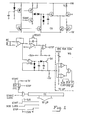
- Figure 1 shows the circuit diagram of an electronic coin validator according to the present invention,
- Figure 2 shows a set of waveforms which are produced at various points in the circuitry of Figure 1,
- Figure 3 shows the output waveforms of the circuitry of Figure 1 for each coin denomination,
- Figure 4 shows a coin validator of another embodiment of the present invention,
- Figure 5 shows a graph of the normalised coil voltage against frequency with a coin present in the embodiment shown in Figure 4.
- Referring to Figures 1,2 and 3, an embodiment of the invention, an impulse test type validator, will now be described.
- For impulse testing the magnetic field is larger than the largest coin to be tested and two parameters are measured, coin face area and coin resistance. The receive coil current waveform is shown in Figure 2. If the open circuit voltage in the coin, is detected, the peak voltage is a measure of a coin face area and the integrated voltage waveform has a time constant related to the coin resistance.
- The circuit of Figure 1, produces the waveforms of Figure 2. It consists of a current switch CS which has a defined turn on time, and drives the transmit coil TC. The receive coil RC drives an amplifier which is connected to an integrator I and a peak detector PD. A comparator set at 90% of the integrator maximum output voltage gives a signal that allows t.coin to be measured, where t coin is the time taken for the integrator output voltage to rise to the 90% level. A start pulse gates a 10 MHz clock into a counter chain CC via flip flop FF1 when the transmit current step is applied, and, the integrator output stops the count. The number in the counter is now a measure of t coin which relates to coin resistance, and may be applied to a microprocessor µP for evaluation. The peak detector holds the peak impulse shown in Figure 2 and can produce the set of output voltages shown in Figure 3 for the different coins. The peak detector drives four window gates WG, one of which is shown, whose thresholds are adjusted to each coin face area distribution. The window comparator outputs are gated into a 'D' type flip-flop FF2 that are clocked 5 u S after the start of the coin test, this effectively produces a peak detector output sample at 5 µ S, as shown in Figure 3. The output of each flip-flop FF2 may be applied to the microprocessorup for evaluation. Alternatively, the peak detector voltage may be entered into an analog-to-digital converter and the output applied to a microprocessor for evaluation.
- The theory of operation of the impulse test type coin validator is as follows:-


- If the step is of rise time T, this is modified to:

- It can be shown that L is large and T small then the rise time variation does not have a great effect on eoc.
- The voltage in the receive coil due to the presence of the coin is modified to:

- Any disc of the correct size will meet the size parameter, but then has to have a time t coin inside the correct time distribution to meet the second parameter and be recognised as genuine.
- The validator uses identical transmit and receive coils wound on the outside of a ferrite vinkor..The area of the coil is quite critical and has to be such as to allow sufficient flux to pass around each coin and also produce an easily measurable t-coin period in excess of 10 uS.
- Referring to Figures 4 and 5 an alternative embodiment of the invention will now be described.
- The multi-frequency validator carries out a test to verify two parameters of the coin. The first parameter is of face area of the coin, and the second parameter is of the coin resistance.
- A magnetic field larger than the largest coin face area is produced across the coin runway between the transmit and receive coils. The field can be either produced by an alternating current or a step change of current in the transmit coil.
- The multi-frequency validator has a transmit coil TC which is driven by a coil drive circuit CD. The coil drive circuit CD is fed with a multi-frequency signal generated from oscillator OSC and divider circuit DV via a signal amplitude control circuit AC, filter circuits F1-F4 and summing and amplitude weighting circuit SW.
- The receive coil RC drives a differential amplifier DA and filters F5-F8. The output of the filters is fed via respective rectifier circuits R1-R3 to detector circuits D1-D3 the outputs of which are selectively switched by switch S to analog-to-digital converter ADO to a microprocessor pP for evaluation.
- Rectifier R4 feeds an automatic gain control circuit AGO which also receives a voltage reference signal from circuit VR. The output of the automatic gain control circuit AGO is used to modify the operation of signal amplitude control circuit AC to compensate for temperature changes in inductance, drift etc. The graph shown in Figure 5 shows the normalized receive coil voltage NCV against transmit current frequency f. At frequencies below 1KHz the received signal amplitude is unaffected by the presence of the coin set of interest and so can be used for a continuous reference tone that compensates for variations in mutual inductance, temperature effects and component drift. At high frequencies the coin is opaque to the applied magnetic field and so the majority of the received signal is due to the field that gets round the edge of the coin, therefore the ratio of the amplitude of the received signal with and without the coin present gives a measure of the coin face area. If amplitude measurements are taken in the receive coil at two frequencies between 1KHz and 100KHz we can get a measure of the coin resistance. The open circuit receive coil voltage is:-


- The term A w cos wt gives a measure of coin face area at high frequency and the other terms at lower frequencies give a measure of coin resistance.

- where NT is Number of turns on the transmit coil
- NR is Number of turns on the receive coil
- µe is the effective permeability
- The equation shows that Voc varies in amplitude with w and M. An accurately controlled frequency using a crystal master clock will prevent variations in w effecting Voc. However, coin face area is the ratio of the magnetic field passing round the coin to that when no coin is present and is directly proportional to the mechanical dimensions of the receive coil, which vary from coil to coil. As a result one absolute adjustment is needed to set up the validator in production and can be carried out with a disc of accurate proportions. The ratios from coin to coin will always be the same once the initial adjustment is made.
Claims (13)
Priority Applications (1)
| Application Number | Priority Date | Filing Date | Title |
|---|---|---|---|
| AT81304000T ATE12710T1 (en) | 1980-09-19 | 1981-09-02 | ELECTRONIC COIN CHECKER. |
Applications Claiming Priority (2)
| Application Number | Priority Date | Filing Date | Title |
|---|---|---|---|
| GB8030389 | 1980-09-19 | ||
| GB8030389 | 1980-09-19 |
Publications (2)
| Publication Number | Publication Date |
|---|---|
| EP0048557A1 true EP0048557A1 (en) | 1982-03-31 |
| EP0048557B1 EP0048557B1 (en) | 1985-04-10 |
Family
ID=10516179
Family Applications (1)
| Application Number | Title | Priority Date | Filing Date |
|---|---|---|---|
| EP81304000A Expired EP0048557B1 (en) | 1980-09-19 | 1981-09-02 | Electronic coin validators |
Country Status (7)
| Country | Link |
|---|---|
| EP (1) | EP0048557B1 (en) |
| AT (1) | ATE12710T1 (en) |
| AU (1) | AU541536B2 (en) |
| DE (1) | DE3169841D1 (en) |
| IE (1) | IE52100B1 (en) |
| ZA (1) | ZA816172B (en) |
| ZW (1) | ZW22881A1 (en) |
Cited By (1)
| Publication number | Priority date | Publication date | Assignee | Title |
|---|---|---|---|---|
| EP0119000A1 (en) * | 1983-02-09 | 1984-09-19 | Cash & Security Equipment Limited | Coin discriminating apparatus |
Citations (9)
| Publication number | Priority date | Publication date | Assignee | Title |
|---|---|---|---|---|
| DE1925042A1 (en) * | 1969-05-16 | 1970-11-26 | Johann Stegmueller | Method for recognizing or determining the dimensions and material of coins and workpieces by means of capacitive and / or inductive probes |
| DE1930345A1 (en) * | 1969-06-14 | 1970-12-23 | Nat Rejectors Gmbh | Arrangement for sorting metal sheets or disks |
| FR2212589A1 (en) * | 1972-12-29 | 1974-07-26 | Satmam | |
| US3962627A (en) * | 1974-12-20 | 1976-06-08 | The Vendo Company | Electronic apparatus for testing moving coins employing successive time significant sensings of the effects of proximity of a coin under test to inductive impedance elements upon the effective impedances thereof |
| DE2551321A1 (en) * | 1975-11-13 | 1977-05-26 | Berliner Maschinenbau Ag | Automatically programmed inductive tester - is for coins or metal discs passing between transmitter and receiver coils and has comparator |
| US4086527A (en) * | 1975-03-25 | 1978-04-25 | Crouzet | Method and apparatus for monetary articles authentification |
| US4091908A (en) * | 1976-02-10 | 1978-05-30 | Nippon Coinco Co., Ltd. | Coin checking device for a vending machine |
| US4108296A (en) * | 1976-04-08 | 1978-08-22 | Nippon Coinco Co., Ltd. | Coin receiving apparatus for a vending machine |
| US4124111A (en) * | 1975-12-02 | 1978-11-07 | Nippon Coinco Co. Ltd. | Coin inspecting apparatus |
-
1981
- 1981-09-02 DE DE8181304000T patent/DE3169841D1/en not_active Expired
- 1981-09-02 EP EP81304000A patent/EP0048557B1/en not_active Expired
- 1981-09-02 AT AT81304000T patent/ATE12710T1/en not_active IP Right Cessation
- 1981-09-04 ZA ZA816172A patent/ZA816172B/en unknown
- 1981-09-11 AU AU75167/81A patent/AU541536B2/en not_active Ceased
- 1981-09-15 ZW ZW228/81A patent/ZW22881A1/en unknown
- 1981-09-18 IE IE2174/81A patent/IE52100B1/en unknown
Patent Citations (9)
| Publication number | Priority date | Publication date | Assignee | Title |
|---|---|---|---|---|
| DE1925042A1 (en) * | 1969-05-16 | 1970-11-26 | Johann Stegmueller | Method for recognizing or determining the dimensions and material of coins and workpieces by means of capacitive and / or inductive probes |
| DE1930345A1 (en) * | 1969-06-14 | 1970-12-23 | Nat Rejectors Gmbh | Arrangement for sorting metal sheets or disks |
| FR2212589A1 (en) * | 1972-12-29 | 1974-07-26 | Satmam | |
| US3962627A (en) * | 1974-12-20 | 1976-06-08 | The Vendo Company | Electronic apparatus for testing moving coins employing successive time significant sensings of the effects of proximity of a coin under test to inductive impedance elements upon the effective impedances thereof |
| US4086527A (en) * | 1975-03-25 | 1978-04-25 | Crouzet | Method and apparatus for monetary articles authentification |
| DE2551321A1 (en) * | 1975-11-13 | 1977-05-26 | Berliner Maschinenbau Ag | Automatically programmed inductive tester - is for coins or metal discs passing between transmitter and receiver coils and has comparator |
| US4124111A (en) * | 1975-12-02 | 1978-11-07 | Nippon Coinco Co. Ltd. | Coin inspecting apparatus |
| US4091908A (en) * | 1976-02-10 | 1978-05-30 | Nippon Coinco Co., Ltd. | Coin checking device for a vending machine |
| US4108296A (en) * | 1976-04-08 | 1978-08-22 | Nippon Coinco Co., Ltd. | Coin receiving apparatus for a vending machine |
Cited By (1)
| Publication number | Priority date | Publication date | Assignee | Title |
|---|---|---|---|---|
| EP0119000A1 (en) * | 1983-02-09 | 1984-09-19 | Cash & Security Equipment Limited | Coin discriminating apparatus |
Also Published As
| Publication number | Publication date |
|---|---|
| ZW22881A1 (en) | 1981-12-09 |
| AU7516781A (en) | 1982-03-25 |
| IE52100B1 (en) | 1987-06-10 |
| DE3169841D1 (en) | 1985-05-15 |
| ZA816172B (en) | 1982-09-29 |
| IE812174L (en) | 1982-03-19 |
| ATE12710T1 (en) | 1985-04-15 |
| AU541536B2 (en) | 1985-01-10 |
| EP0048557B1 (en) | 1985-04-10 |
Similar Documents
| Publication | Publication Date | Title |
|---|---|---|
| EP0119000B1 (en) | Coin discriminating apparatus | |
| US4436196A (en) | Method of and apparatus for assessing coins | |
| EP0202378A2 (en) | Coin selection apparatus | |
| US5573099A (en) | Apparatus and method for identifying metallic tokens and coins | |
| GB2029995A (en) | Metal detectors | |
| SE442458B (en) | DEVICE FOR THE CONTROL OF METAL FORM, Separate coin, INCLUDING AN ELECTROMAGNETIC DETECTOR | |
| IE38359B1 (en) | Phase sensitive coin discrimination method and apparatus | |
| EP0404432B1 (en) | Microprocessor-controlled apparatus adaptable to environmental changes | |
| CA2162364C (en) | Money validation | |
| EP0203702B1 (en) | Moving coin validation | |
| EP0048557A1 (en) | Electronic coin validators | |
| GB2135095A (en) | Coin discriminating apparatus | |
| US6536578B1 (en) | Sensor for coin acceptor | |
| GB2084370A (en) | Electronic Coin Validator | |
| EP0527874B1 (en) | Method and apparatus for testing coins | |
| US4846332A (en) | Counterfeit coin detector circuit | |
| PL177877B1 (en) | Apparatus for verifying authenticity of coins, tokens or other flat metal objects | |
| SU1760310A1 (en) | Distance noncontact measuring device | |
| JPS5856155B2 (en) | coin sorting device | |
| JP4369626B2 (en) | Coin identification sensor and coin identification method | |
| JPS6346479B2 (en) | ||
| KR880002151B1 (en) | Improvements in and relating to apparatus for checking the validity of coins | |
| JPS63301392A (en) | Coin selector | |
| JPS5846754B2 (en) | Coin nosen betsusou | |
| JP2000504862A (en) | Coin diameter measurement |
Legal Events
| Date | Code | Title | Description |
|---|---|---|---|
| PUAI | Public reference made under article 153(3) epc to a published international application that has entered the european phase |
Free format text: ORIGINAL CODE: 0009012 |
|
| AK | Designated contracting states |
Designated state(s): AT CH DE IT NL SE |
|
| 17P | Request for examination filed |
Effective date: 19820831 |
|
| ITF | It: translation for a ep patent filed |
Owner name: ING. C. GREGORJ S.P.A. |
|
| GRAA | (expected) grant |
Free format text: ORIGINAL CODE: 0009210 |
|
| AK | Designated contracting states |
Designated state(s): AT CH DE IT LI NL SE |
|
| REF | Corresponds to: |
Ref document number: 12710 Country of ref document: AT Date of ref document: 19850415 Kind code of ref document: T |
|
| REF | Corresponds to: |
Ref document number: 3169841 Country of ref document: DE Date of ref document: 19850515 |
|
| PLBE | No opposition filed within time limit |
Free format text: ORIGINAL CODE: 0009261 |
|
| STAA | Information on the status of an ep patent application or granted ep patent |
Free format text: STATUS: NO OPPOSITION FILED WITHIN TIME LIMIT |
|
| 26N | No opposition filed | ||
| PGFP | Annual fee paid to national office [announced via postgrant information from national office to epo] |
Ref country code: AT Payment date: 19860910 Year of fee payment: 6 |
|
| PGFP | Annual fee paid to national office [announced via postgrant information from national office to epo] |
Ref country code: NL Payment date: 19870930 Year of fee payment: 7 |
|
| PGFP | Annual fee paid to national office [announced via postgrant information from national office to epo] |
Ref country code: SE Payment date: 19890619 Year of fee payment: 9 |
|
| PG25 | Lapsed in a contracting state [announced via postgrant information from national office to epo] |
Ref country code: AT Effective date: 19890902 |
|
| PG25 | Lapsed in a contracting state [announced via postgrant information from national office to epo] |
Ref country code: LI Effective date: 19890930 Ref country code: CH Effective date: 19890930 |
|
| PG25 | Lapsed in a contracting state [announced via postgrant information from national office to epo] |
Ref country code: NL Effective date: 19900401 |
|
| NLS | Nl: assignments of ep-patents |
Owner name: GEC PLESSEY TELECOMMUNICATIONS LIMITED TE COVENTRY |
|
| NLV4 | Nl: lapsed or anulled due to non-payment of the annual fee | ||
| REG | Reference to a national code |
Ref country code: CH Ref legal event code: PL |
|
| PG25 | Lapsed in a contracting state [announced via postgrant information from national office to epo] |
Ref country code: DE Effective date: 19900601 |
|
| ITPR | It: changes in ownership of a european patent |
Owner name: CESSIONE;GEC PLESSEY TELECOMUNICATIONS LIMITED |
|
| PG25 | Lapsed in a contracting state [announced via postgrant information from national office to epo] |
Ref country code: SE Effective date: 19900903 |
|
| EUG | Se: european patent has lapsed |
Ref document number: 81304000.3 Effective date: 19910527 |