EP0050005A2 - Semiconductor memory with improved data programming time - Google Patents
Semiconductor memory with improved data programming time Download PDFInfo
- Publication number
- EP0050005A2 EP0050005A2 EP81304660A EP81304660A EP0050005A2 EP 0050005 A2 EP0050005 A2 EP 0050005A2 EP 81304660 A EP81304660 A EP 81304660A EP 81304660 A EP81304660 A EP 81304660A EP 0050005 A2 EP0050005 A2 EP 0050005A2
- Authority
- EP
- European Patent Office
- Prior art keywords
- column
- memory
- row
- data
- lines
- Prior art date
- Legal status (The legal status is an assumption and is not a legal conclusion. Google has not performed a legal analysis and makes no representation as to the accuracy of the status listed.)
- Granted
Links
Images


Classifications
-
- G—PHYSICS
- G11—INFORMATION STORAGE
- G11C—STATIC STORES
- G11C29/00—Checking stores for correct operation ; Subsequent repair; Testing stores during standby or offline operation
- G11C29/04—Detection or location of defective memory elements, e.g. cell constructio details, timing of test signals
- G11C29/08—Functional testing, e.g. testing during refresh, power-on self testing [POST] or distributed testing
- G11C29/12—Built-in arrangements for testing, e.g. built-in self testing [BIST] or interconnection details
- G11C29/18—Address generation devices; Devices for accessing memories, e.g. details of addressing circuits
- G11C29/30—Accessing single arrays
- G11C29/34—Accessing multiple bits simultaneously
-
- G—PHYSICS
- G11—INFORMATION STORAGE
- G11C—STATIC STORES
- G11C16/00—Erasable programmable read-only memories
- G11C16/02—Erasable programmable read-only memories electrically programmable
- G11C16/06—Auxiliary circuits, e.g. for writing into memory
- G11C16/08—Address circuits; Decoders; Word-line control circuits
-
- G—PHYSICS
- G11—INFORMATION STORAGE
- G11C—STATIC STORES
- G11C16/00—Erasable programmable read-only memories
- G11C16/02—Erasable programmable read-only memories electrically programmable
- G11C16/06—Auxiliary circuits, e.g. for writing into memory
- G11C16/10—Programming or data input circuits
- G11C16/12—Programming voltage switching circuits
-
- G—PHYSICS
- G11—INFORMATION STORAGE
- G11C—STATIC STORES
- G11C16/00—Erasable programmable read-only memories
- G11C16/02—Erasable programmable read-only memories electrically programmable
- G11C16/06—Auxiliary circuits, e.g. for writing into memory
- G11C16/32—Timing circuits
-
- G—PHYSICS
- G11—INFORMATION STORAGE
- G11C—STATIC STORES
- G11C7/00—Arrangements for writing information into, or reading information out from, a digital store
- G11C7/22—Read-write [R-W] timing or clocking circuits; Read-write [R-W] control signal generators or management
-
- G—PHYSICS
- G11—INFORMATION STORAGE
- G11C—STATIC STORES
- G11C8/00—Arrangements for selecting an address in a digital store
- G11C8/12—Group selection circuits, e.g. for memory block selection, chip selection, array selection
Definitions
- the present invention relates to a semiconductor memory and, more particularly, a nonvolatile semiconductor memory using, as memory cells, field effect transistors each including a floating gate within a gate insulating film.
- a program voltage (e.g. 25 V) is simultaneously applied to the gate and drain of a memory insulating gate field effect transistor.
- a program voltage e.g. 25 V
- about 50 milliseconds are taken to program a single memory cell. In this case, the programming is performed every word. Accordingly, about 1.7 minutes are taken to program all the memory cells of a memory of 2048 words x 8 bits, and about 3.4 minutes for a memory of 4096 words x 8 bits.
- an object of the present invention is to provide a nonvolatile semiconductor memory which simultaneously programs a plurality of memory cells with different addresses to thereby reduce a data programming time.
- a semiconductor memory comprises a memory array including a plurality of memory cells, such as floating-gate type MOS transistors, arranged in a matrix form having column lines and row lines and a plurality of bit outputs. Each bit output is associated with a plurality of column lines.
- a row decoder and a column decoder for selecting a plurality of memory cells for one word.
- a circuit which responds to a control signal or signals to simultaneously apply a program voltage to a plurality of column lines corresponding to 1-bit output so that memory cells of different addresses are simultaneously programmed.
- the column lines associated with each output bit are divided into a plurality of groups.
- One of the column lines in each of the column line groups is selected by the column decoder.
- a data input circuit applies a program voltage to a plurality of column lines corresponding to one bit output selected by the column decoder in response to in-phase address signals.
- a plurality of memory cells connected with one row line selected by the row decoder and the column lines to which the program voltage is applied are simultaneously programmed.
- the memory array is divided into a plurality of memory array blocks.
- One of the memory array blocks is selected by address signals.
- a pair of address signals is made in-phase by a control signal, so that a plurality of memory array blocks are selected and memory cells addressed by decoders, in each of the selected memory blocks, are simultaneously programmed.
- a plurality of column lines associated with each bit output in the memory array are divided into a plurality of groups.
- One of the column lines of each of the column line groups is connected to an output of the column decoder.
- Each column line group is connected through a switch element to a program power source.
- a data input circuit to which input data having more than two voltage levels is applied, controls the switching elements on the basis of a voltage level of the input data applied, so that data 1 and/or data 0 is written into a plurality of memory cells associated with each bit output and selected by column and row decoders.
- a nonvolatile semiconductor memory which comprises a memory array 1 having row lines 1 0 , 1 1 , ..., column lines 2 0 , 21, ..., and floating gate type MOS transistors 3 11 , 3 12 , ..., 3 21 , 3 22 , ... acting as memory cells.
- the MOS transistors have their sources grounded, their drains connected to corresponding column lines, and their gates connected with corresponding row lines.
- the row lines 1 0 , 1 1 , ... are connected to a row (x) decoder 4. Ends of the column lines 2 0 , 2 1 , ... are connected with a power source of program voltage Vp via insulating-gate field effect transistors (IGFET) 5 0 , 5 1 , 5 2 , 5 3 , .... The other ends of the column lines are coupled with a common terminal 7 by way of column se- lect i n g IGFET's 60 , 6 1 , ....
- Gates of the IGFET's 5 0 , 5 2 , ..., are supplied with a gate signal Yl, while gates of the IGFET's 5 1 , 5 3 , ..., are supplied with a gate signal Y2.
- Gates of the IGFET's 6 0 , 6 1 , ... are connected with the corresponding outputs (column selecting lines) of a column decoder 8.
- the common terminal 7 is coupled with the source of program voltage Vp through an IGFET 9 having its gate coupled with the output of a data input circuit 10 supplied with input data.
- the common terminal 7 is connected to a sense amplifier/output buffer circuit 12 through an IGFET 11 supplied with a data readout instruction signal R/W at its gate.
- the input terminal of sense amplifier 12 is connected with a power source Vc (5 V, for example) via a depletion mode IGFET 13 having its gate connected with the input of sense amplifier 12.
- the sense amplifier 12 provides a 1 output bit. When one word stored in the memory consists of 4 bits, or the memory has 4 bit outputs, four sense amplifiers are provided. The same thing is true for the data input circuit 10.
- the IGFET's 5 0 , 5 1 , 5 2 , 5 3 , ... are turned on by raising the levels of gate signals Yl and Y2 up to the program voltage Vp.
- the program voltage Vp is applied to all the column lines.
- the gates and drains of the floating-gate IGFET's connected with each row line are supplied with voltages Vp and (Vp - Vth), respectively, so that memory transistors are programmed.
- Vth represents a threshold voltage of each of IGFET's 5 0 , 5 1 , 5 2 , 5 3 , ....
- the gate signals Yl and Y2 may be alternately raised to the program voltage Vp such that the gate signal Yl is raised when row line 1 0 is selected and the gate signal Y2 is raised when the row line 1 1 is selected.
- data 1 is written into alternate memory cells connected to each row line, and data 0 is written into the remaining memory cells.
- data 1 represents a state that electrons are not injected into the floating gate of memory cell, while data 0 represents a state that electrons have been injected into the floating gate.
- the gate signals Yl and Y2 are raised up to the program voltage Vp only during the test process of memory devices, and therefore the gate signals are zero volt during a formal data programming time.
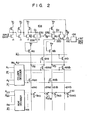
- Fig. 2 shows another embodiment of a nonvolatile semiconductor memory of the present invention.
- the program voltage Vp is simultaneously applied to two of the column lines for one output bit which are selected by the column decoder so that a couple of memory cells connected to a row line selected by the row decoder are simultaneously programmed.
- a pair of common terminals 7a and 7b are provided which are coupled to the program voltage Vp through IGFET's 9a and 9b.
- the common terminals 7a and 7b are connected to a data readout FET lla followed by sense amplifier 12a, by way of IGFET's 21a and 21b supplied with address signals AO and A0, respectively.
- common terminal 7a is coupled with column lines 2oa to 2ma via column selecting FET's 6oa to 6ma, gates of which are connected to the outputs of column decoder 8a, respectively.
- the common terminal 7b is connected with column lines 2ob to 2mb by way of column selecting FET's 6ob to 6mb, having gates connected with the outputs of column decoder 8a, respectively.
- Column lines 2oa to 2ma and 2ob to 2mb are connected to drains of floating-gate FET's 3 11 a to 3 1ma and 3 11b to 3 1ma .
- Gates of IGFET's 9a and 9b are respectively connected to output terminals 0 1 and 0 2 of data input circuit 10a.
- Output terminal 0 1 is grounded through an IGFET 22a and an IGFET 23a.
- the gate of IGFET 22a is supplied with address signal AO
- the gate of IGFET 23a is supplied with an R/W signal.
- output terminal 0 2 is grounded through an IGFET 22b and an IGFET 23b.
- the gate of IGFET 22b is supplied with address signal AO and the gate of IGFET 23b is supplied with R
- the address input signals A0 and AO and the R/W signal are set at logic 0 level.
- IGFET's lla, 21a, 21b, 22a, 22b, 23a and 23b are turned off.
- output terminals 0 1 and 0 2 go to the logic 1 level (in this case, Vp level), to turn ON IGFET's 9a and 9b.
- Vp level logic 1 level
- address signals AO and AO are set in a complementary relation.
- IGFET 22b is ON. Therefore, output terminal 0 2 is at substantially ground level, and the IGFET 9b is OFF.
- output terminal 0 1 goes to logic 1 level or logic 0 level. Consequently, one memory cell selected by row decoder 4a and column decoder 8a is written with data of 0 or 1.
- data 1 corresponds to logic 1 of input data.
- the terminal 0 1 is at logic 0 level and transistor 9a remains off. Namely, writing data 1 into a memory cell means that the floating-gate of memory cell is neutral.
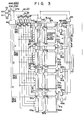
- Fig. 3 shows yet another embodiment of a nonvolatile semiconductor memory of the present invention.
- the memory array is divided into four blocks. And the corresponding memory cells in four or two memory blocks (16 or 8 cells when a word consists of 4 bits) are simultaneously programmed.
- reference numerals 31 1 to 31 4 designate the memory blocks. These memory blocks include respectively memory arrays 32 1 to 32 4 , row decoders 33 1 to 33 4 , column decoder 34 1 to 34 4 , column selecting gate circuits 35 1 to 35 4 , write load circuits 36 1 to 36 4 and write load circuit 37 1 to 37 4 .
- memory arrays 32 1 to 32 4 are each a 64 (16 x 40) words by 4 bits array.
- Address signals A2 to A5 are applied to each of row decoders 33 1 to 33 4 via address buffers 38 to 41, respectively, while address signals A6 and A7 are applied to each of column decoders 34 1 to 34 4 by way of address buffers 42 and 43.
- Selection of the memory blocks 31 1 to 31 4 is performed by output signals MS1, MS1 to MS4 and MS4 of a memory block selecting circuit 44 fed with address signals A 0 and Al.
- Write load circuits 36 1 to 36 4 and 37 1 to 37 4 are selectively enabled by output signals R /W1, R/W2, R/W3 and R/W4 of a load-circuit selecting circuit 45 supplied with address signals AO and Al.
- the 4-bit outputs of each of memory blocks 31 1 to 31 4 are coupled together with an output circuit 47 via transmission gate circuits 46 1 to 46 4 .
- To memory blocks 31 1 to 31 4 are connected write circuits 48 1 to 48 4 which are selectively enabled by output signals WS1 to WS4 of write-circuit selecting circuit 49.
- Circuits 48 1 to 48 4 each supply input data Din from an input circuit 50 to the corresponding memory block when enabled.
- a multiple-write circuit designated by reference numeral 51 is arranged to supply signals MWl (MW2) and MWl (MW2) to address buffers 52 and 53 to which the address signals AO and Al are supplied in order to set the address signals to the multiple write mode in which a plurality of memory blocks are selected and a plurality of memory cells in the selected memory blocks are concurrently programmed.
- Fig. 4 shows a practical arrangement of multiple-write circuit 51.
- Reference numerals 61 to 64 designate depletion mode IGFET's and reference numerals 65 to 68 enhancement mode IGFET's.
- Address signal A0 (or Al) is applied to an inverter 69 for detecting an input voltage of 10 V or more as a logic 1.
- the output signal MWl (MW2) goes to logic 1 level, while the output signal MWl (MW2) goes to logic 0 level, thus instructing address buffers 52 and 53 to execute the multiple-write.
- the address signal AO (Al) is below 10 V. Under this condition, the output signal MWl (MW2) is at logic 0 level, while the output signal (MWl) (MW2) is at logic 1 level.
- Fig. 5 shows a practical arrangement of the address buffer 52 (or 53).
- Reference numerals 71 to 74 designate IGFET's the threshold voltage of which is 0 V; reference numerals 75 to 77 depletion mode IGFET's; 78 to 86 enhancement mode IGFET's.
- the output signals MW1 (MW2) and MWl (MW2) of multiple-write circuit 51 are respectively at logic 0 and logic 1 level. Therefore, output signals a0 (al) and aO (al) of address buffer 52 (53) are at comple- mentray logic levels according to the logic level of the address signal AO (Al).
- the address buffer circuits shown in Figs. 4 and 5 can be used in the memories shown in Figs. 1 and 2. If the address buffer circuit is used for address input signals to the row decoder, then a plurality of row lines can be selected concurrently so that memory cells connected to the plurality of row lines are programmed at the same time. This means, as stated above, that program data are simultaneously applied to the memory cells. For programming test, data applied to the memory cells may be identical to each other.
- Fig. 6 shows a practical arrangement of memory block selecting circuit 44.
- Reference numerals 91 to 94 designate depletion mode IGFET's and numerals 95 to 99 enhancement mode IGFET's. This circuit is provided for each of combinations of the output signals from address buffers 52 and 53; a0 and al, a0 and al; a0 and al, and a 0 and a l.
- the circuit shown in Fig. 6, receives the output signals a0 (a0) and al (al) from address buffers 52 and 53 to form output signals MS1 (MS4) and MS1 (MS4).
- one of the output signals MS1 to MS4 for selecting a memory block designated is at logic 1 level and corresponding one of the signals MSl to MS4 is at logic 0 level.
- the signals a0, aO, al, and al are at logic 0, and hence the signals MS1 to MS4 are all at logic 1, while signals MS1 to MS4 are all at logic 0.
- memory blocks 32 1 to 32 4 are all selected.
- Fig. 7 shows a practical arrangement of the row (column) decoder.
- Reference numeral 101 designates an IGFET the threshold voltage of which is approximately 0 V; numerals 102 to 104 depletion mode IGFET's; and numerals 105 to 109 enhancement mode IGFET's.
- this circuit is provided for each of 16 combinations of the address input signals.
- this circuit is provided for each of four combinations of the address input signals.
- the decode outputs or the row or column selecting lines, take a logical state according to address signals.
- the signals MSl to MS4 are all at logic 1 and the signals MSI to MS4 are all at logic 0, so that all of the memory blocks 32 1 to 32 4 are selected.
- Fig. 8 shows a practical arrangement of the selecting circuit 45 for the write load circuits.
- Reference numerals 111 to 113 designate depletion mode IGFET's and numerals 115 to 118 enhancement mode IGFET's.
- Fig. 9 shows a practical arrangement of the write load circuit.
- Fig. 10 shows a practical arrangement of the write circuit 48 1 .
- reference numerals 123 to 133 designate depletion mode IGFET's and numerals 134 to 138 enhancement mode IGFET's.
- the remaining write circuits 48 2 to 48 4 are also constructed similarly.
- the signals WS2, WS3 and SW4 are supplied to the FET's corresponding to FET 136.
- the memory thus constructed can simultaneously program a memory array of four memory blocks, so that a program test time is reduced to 1/4 that of the prior art memory.
- the address signals A0 and Al are simultaneously set in the multiple-write mode, four memory blocks are simultaneously selected.
- one of the address signals A0 and Al may be set in the multiple-write mode. In this case, two memory blocks are simultaneously selected.
- a common multiple-write switching circuit may be provided for address buffers 52 and 53. In this case, four memory blocks are simultaneously selected.
- the address signal is used for the multiple-write switching signal, but other signals may be used instead.
- a terminal (pad) exclusively used for the program test may be provided to which a multiple-write switching signal is supplied.
- Fig. 11 shows a modification of the memory of Fig. 3 in which row and column decoders are used commonly for the memory blocks. Outputs of row selecting gate circuits 35 1 to 35 4 are coupled to an output circuit 47 through sense amplifiers 54 1 to 54 4 .
- the memory block selecting circuit 44 selects one of the memory blocks so that the-write circuit and the sense amplifier in the memory block are enabled.
- the write circuits are all enabled to write data into memory cells, selected by row and column decoders 33 and 34, in the memory arrays 32 1 to 32 4 .
- memory blocks 31 1 to 31 4 and output circuit 47 each are arranged to have 4 bit outputs. However, they may have 1 bit output. With a 4-bit output memory device, if memory blocks 31 1 to 31 4 and output circuit 47 each have 1 bit output, then four-memory block unit and output circuit are further necessitated.
- Fig. 12 shows still another embodiment of a nonvolatile semiconductor memory according to the present invention.
- This circuit is different from the circuit of Fig. 2 with respect to only data input circuit. Accordingly, like numerals are used for like portions in F ig. 2.
- a plurality of column lines associated with one output bit are divided into a plurality of groups.
- Data 1 and/or 0 are written into memory cells which are connected to corresponding column lines in the groups selected by the column decoder and a row line selected by the row decoder, for the purpose of the data programming.
- the contents of data written into the memory cells are determined by a data input circuit 10b which detects a voltage level of the input data having more than 2 voltage levels.
- the present embodiment is suitable for the program test and the normal data programming as well.
- An input data voltage applied to data input circuit 10b is set at 0 V, 5 V, 10 V or 15 V. Relationships between logic levels of outputs s and t of data input circuit 10b and input data voltage are shown in Table 1 given below.
- the logic 1 level of output s and t indicates the program voltage Vp (25 V), while the logic 0 level indicates 0 V.
- FET 9b turns on. At this time, if the row line loa and the column line 2ob are selected by decoders 4a and 8a, logic 1 data is written into memory cell 3 11b . Since FET 9a remains off, the content of memory cell 3 11 a remains zero. In other words, zero is written into memory cell 3 11a .
- Fig. 13 a practical arrangement of the data input circuit for executing logic functions shown in the Table 1 is illustrated.
- logic levels of outputs s and t of the circuit and at points of X, Y and Z are tabulated.
- the logic 1 level at points X, Y and Z indicates a voltage Vc (5 V, for example), and the logic 1 level of outputs s and t represents the program voltage Vp.
- reference numerals 141, 142 and 143 designate reference voltage generating circuits which are enabled by the signal R/W to generate reference voltages of 2 V, 7 V and 12 V, respectively.
- the reference voltages 2 V, 7 V and 12 V are compared with the voltage of input data by voltage comparators 144, 145 and 146, respectively.
- gate circuits 147 to 150 are controlld to determine the logic levels at outputs s and t.
- FIG. 14 another arrangement of data input circuit 10b is shown.
- a reference voltage generating section 161 generates reference voltages of 7 V, 12 V, 18 V and 21 V. These reference voltages are compared with the input data voltage in the voltage comparator 162 to 165, respectively.
- This circuit can write 1 into one memory cell selected by address signals when the input data is at 5 V.
- the input data is at 10 V, 15 V, 20 V or 25 V, a pair of memory cells having different addresses can be simultaneously programmed. Further, two-bit program data can be applied to two memory cells at the same time.
- the circuit of Fig. 14 operates according to Table 3 given below.
- program data can be applied to a plurality of memory cells at the same time. Therefore, a data latch time is not necessary.
- a memory area corresponding to 1 output bit is divided into two groups. Therefore, the programming time is halved compared with that of the prior art. Generally, if the memory area is divided into n groups, the programming time is reduced to 1/n of that of the prior art. And in this case, the input data has 2 n voltage levels.
- the number of the aforesaid gate signals Yl, Y2 is not limited to two, but may be three or more.
- the signals Yl, Y2 may be supplied through input pads.
- input signals for example, address input signals
- the present invention is also applicable to a RAM (random access memory). Namely, also in a read/write RAM memory cells having different addresses can be selected and written simultaneously by using a special signal according to the teachings described in connection with the illustrated embodiments of this invention. Further, through the embodiment of this invention were described in connection with 1 word x 4 bit memory, this invention may be applied to 1 word x 1 bit memory or 1 word x 8 bit memory.
Abstract
Description
- The present invention relates to a semiconductor memory and, more particularly, a nonvolatile semiconductor memory using, as memory cells, field effect transistors each including a floating gate within a gate insulating film.
- In a nonvolatile semiconductor memory such as an erasable and electrically programmable read only memory (EPROM) using field effect transistors each having a floating gate within an insulating film, to program a memory cell, that is, to inject electrons into the floating gate, a program voltage (e.g. 25 V) is simultaneously applied to the gate and drain of a memory insulating gate field effect transistor. Usually, about 50 milliseconds are taken to program a single memory cell. In this case, the programming is performed every word. Accordingly, about 1.7 minutes are taken to program all the memory cells of a memory of 2048 words x 8 bits, and about 3.4 minutes for a memory of 4096 words x 8 bits.
- In the die sort process of semiconductor memories, all the dies on a single wafer are tested as to whether all the memory cells can be programmed or not. In the case of the memory of 4096 words x 8 bits, if 150 dies, for example, fabricated on a single wafer, time taken for the programming test of all of the dies is 3.4 minutes x 150 = 510 minutes, or 8.5 hours.
- The same thing can be said for actual data programming of semiconductor memories. A long programming time is taken for programming memories word by word.
- Accordingly, an object of the present invention is to provide a nonvolatile semiconductor memory which simultaneously programs a plurality of memory cells with different addresses to thereby reduce a data programming time.
- A semiconductor memory according to the present invention comprises a memory array including a plurality of memory cells, such as floating-gate type MOS transistors, arranged in a matrix form having column lines and row lines and a plurality of bit outputs. Each bit output is associated with a plurality of column lines. To the memory array is connected a row decoder and a column decoder for selecting a plurality of memory cells for one word.
- According to one embodiment of the present invention, a circuit is provided which responds to a control signal or signals to simultaneously apply a program voltage to a plurality of column lines corresponding to 1-bit output so that memory cells of different addresses are simultaneously programmed.
- According to a second embodiment, the column lines associated with each output bit are divided into a plurality of groups. One of the column lines in each of the column line groups is selected by the column decoder. A data input circuit applies a program voltage to a plurality of column lines corresponding to one bit output selected by the column decoder in response to in-phase address signals. As a result, a plurality of memory cells connected with one row line selected by the row decoder and the column lines to which the program voltage is applied are simultaneously programmed.
- According to a third embodiment of the present invention, the memory array is divided into a plurality of memory array blocks. One of the memory array blocks is selected by address signals. In a simultaneous data write mode, a pair of address signals is made in-phase by a control signal, so that a plurality of memory array blocks are selected and memory cells addressed by decoders, in each of the selected memory blocks, are simultaneously programmed.
- According to a fourth embodiment of the present invention, a plurality of column lines associated with each bit output in the memory array are divided into a plurality of groups. One of the column lines of each of the column line groups is connected to an output of the column decoder. Each column line group is connected through a switch element to a program power source. A data input circuit, to which input data having more than two voltage levels is applied, controls the switching elements on the basis of a voltage level of the input data applied, so that
data 1 and/or data 0 is written into a plurality of memory cells associated with each bit output and selected by column and row decoders. - This invention can be more fully understood from the following detailed description when taken in conjunction with the accompanying drawings, in which:
- Fig. 1 schematically shows a nonvolatile memory according to an embodiment of the present invention;
- Fig. 2 schematically shows a nonvolatile memory according to another embodiment of the present invention;
- Fig. 3 illustrates a nonvolatile memory according to still another embodiment of the present invention;
- Fig. 4 shows a practical arrangement of a multiple-write switching circuit used in the memory shown in Fig. 3;
- Fig. 5 shows a practical arrangement of an address buffer circuit controlled by the multiple-write switching circuit in Fig. 3;
- Fig. 6 shows a practical arrangement of a memory block selecting circuit in Fig. 3;
- Fig. 7 illustrates a practical arrangement of row and column decoders in Fig. 3;
- Fig. 8 shows a practical arrangement of a selecting circuit for write-load circuits in Fig. 3;
- Fig. 9 shows a practical arrangement of the write-load circuits in Fig. 3;
- Fig. 10 shows a practical arrangement of a data- write circuit in Fig. 3;
- Fig. 11 shows a modification of the memory in Fig. 3;
- Fig. 12 schematically shows a memory according to still another embodiment of the present invention; and
- Figs. 13 and 14 show practical arrangements of a data input circuit in Fig. 12.
- Referring to Fig. 1, there is shown a nonvolatile semiconductor memory according to an embodiment of the present invention which comprises a
memory array 1 having rowlines column lines 20, 21, ..., and floating gate type MOS transistors 311, 312, ..., 321, 322, ... acting as memory cells. The MOS transistors have their sources grounded, their drains connected to corresponding column lines, and their gates connected with corresponding row lines. - The
row lines decoder 4. Ends of thecolumn lines column decoder 8. The common terminal 7 is coupled with the source of program voltage Vp through an IGFET 9 having its gate coupled with the output of adata input circuit 10 supplied with input data. The common terminal 7 is connected to a sense amplifier/output buffer circuit 12 through an IGFET 11 supplied with a data readout instruction signal R/W at its gate. The input terminal ofsense amplifier 12 is connected with a power source Vc (5 V, for example) via a depletion mode IGFET 13 having its gate connected with the input ofsense amplifier 12. - The
sense amplifier 12 provides a 1 output bit. When one word stored in the memory consists of 4 bits, or the memory has 4 bit outputs, four sense amplifiers are provided. The same thing is true for thedata input circuit 10. - In order to examine whether all of the memory cells of the nonvolatile memory can be written or not, the IGFET's 50, 51, 52, 53, ..., are turned on by raising the levels of gate signals Yl and Y2 up to the program voltage Vp. As a result, the program voltage Vp is applied to all the column lines. Under this condition, when the levels of
row lines row decoder 4, the gates and drains of the floating-gate IGFET's connected with each row line are supplied with voltages Vp and (Vp - Vth), respectively, so that memory transistors are programmed. Vth represents a threshold voltage of each of IGFET's 50, 51, 52, 53, .... - As described above, with this memory, since all of the memory cells connected to the respective row lines are programmed simultaneously, a program test time is remarkably reduced compared with a conventional memory. The memory cells are not only simultaneously programmed but also supplied with program data at the same time. Namely, this obviates the necessity of a special circuit for simultaneous data programming such as a latch circuit.
- Alternatively, the gate signals Yl and Y2 may be alternately raised to the program voltage Vp such that the gate signal Yl is raised when
row line 10 is selected and the gate signal Y2 is raised when therow line 11 is selected. In this case,data 1 is written into alternate memory cells connected to each row line, and data 0 is written into the remaining memory cells. In this case,data 1 represents a state that electrons are not injected into the floating gate of memory cell, while data 0 represents a state that electrons have been injected into the floating gate. It is to be understood that the gate signals Yl and Y2 are raised up to the program voltage Vp only during the test process of memory devices, and therefore the gate signals are zero volt during a formal data programming time. - Fig. 2 shows another embodiment of a nonvolatile semiconductor memory of the present invention. With this embodiment, by making a pair of column selecting address signals in-phase, the program voltage Vp is simultaneously applied to two of the column lines for one output bit which are selected by the column decoder so that a couple of memory cells connected to a row line selected by the row decoder are simultaneously programmed.
- As shown in Fig. 2, in this embodiment, a pair of
common terminals 7a and 7b are provided which are coupled to the program voltage Vp through IGFET's 9a and 9b. Thecommon terminals 7a and 7b are connected to a data readout FET lla followed by sense amplifier 12a, by way of IGFET's 21a and 21b supplied with address signals AO and A0, respectively. Further, common terminal 7a is coupled with column lines 2oa to 2ma via column selecting FET's 6oa to 6ma, gates of which are connected to the outputs of column decoder 8a, respectively. Thecommon terminal 7b is connected with column lines 2ob to 2mb by way of column selecting FET's 6ob to 6mb, having gates connected with the outputs of column decoder 8a, respectively. Column lines 2oa to 2ma and 2ob to 2mb are connected to drains of floating-gate FET's 311a to 31ma and 311b to 31ma. Gates of IGFET's 9a and 9b are respectively connected to output terminals 01 and 02 of data input circuit 10a. Output terminal 01 is grounded through an IGFET 22a and anIGFET 23a. The gate of IGFET 22a is supplied with address signal AO, and the gate ofIGFET 23a is supplied with an R/W signal. On the other hand, output terminal 02 is grounded through anIGFET 22b and anIGFET 23b. The gate ofIGFET 22b is supplied with address signal AO and the gate ofIGFET 23b is supplied with R/W signal. - In the memory arranged as above, in order to write data into memory cells for a program test, the address input signals A0 and AO and the R/W signal are set at logic 0 level. As a result, IGFET's lla, 21a, 21b, 22a, 22b, 23a and 23b are turned off. Under this condition, when logic 0 data is applied to data input circuit 10a, output terminals 01 and 02 go to the
logic 1 level (in this case, Vp level), to turn ON IGFET's 9a and 9b. This means that program data is simultaneously applied to two memory cells. As a result,common terminals 7a and 7b are connected with the program voltage Vp, so that the program voltage Vp is applied to a pair of the column lines selected by column decoder 8a. This implies that a couple of memory cells connected to the selected column lines and the row line selected by row decoder 4a are programmed simultaneously. For example, in Fig. 2, either a pair of memory cells 3lla and 311b or 31ma and 3lmb is simultaneously programmed. Thus, in the memory shown in Fig. 2, the program test time is halved compared with the prior art memory. As stated above, the requirement of a data latch circuit for data programming is obviated. - In Fig. 2, in order to write memory cells formally, address signals AO and AO are set in a complementary relation. For example, when AO = 1 and AO = 0,
IGFET 22b is ON. Therefore, output terminal 02 is at substantially ground level, and theIGFET 9b is OFF. Meanwhile, depending on input data, output terminal 01 goes tologic 1 level or logic 0 level. Consequently, one memory cell selected by row decoder 4a and column decoder 8a is written with data of 0 or 1. In this case,data 1 corresponds tologic 1 of input data. At this time, the terminal 01 is at logic 0 level andtransistor 9a remains off. Namely, writingdata 1 into a memory cell means that the floating-gate of memory cell is neutral. - Fig. 3 shows yet another embodiment of a nonvolatile semiconductor memory of the present invention. In this embodiment, the memory array is divided into four blocks. And the corresponding memory cells in four or two memory blocks (16 or 8 cells when a word consists of 4 bits) are simultaneously programmed.
- In Fig. 3,
reference numerals 311 to 314 designate the memory blocks. These memory blocks include respectively memory arrays 321 to 324,row decoders 331 to 334,column decoder 341 to 344, column selectinggate circuits 351 to 354, writeload circuits 361 to 364 and writeload circuit 371 to 374. In this embodiment, memory arrays 321 to 324 are each a 64 (16 x 40) words by 4 bits array. - Address signals A2 to A5 are applied to each of
row decoders 331 to 334 via address buffers 38 to 41, respectively, while address signals A6 and A7 are applied to each ofcolumn decoders 341 to 344 by way of address buffers 42 and 43. - Selection of the memory blocks 311 to 314 is performed by output signals MS1, MS1 to MS4 and MS4 of a memory
block selecting circuit 44 fed with address signals A0 and Al. Writeload circuits 361 to 364 and 371 to 374 are selectively enabled by output signalsR /W1, R/W2, R/W3 and R/W4 of a load-circuit selecting circuit 45 supplied with address signals AO and Al. - The 4-bit outputs of each of memory blocks 311 to 314 are coupled together with an
output circuit 47 via transmission gate circuits 461 to 464. To memory blocks 311 to 314 are connectedwrite circuits 481 to 484 which are selectively enabled by output signals WS1 to WS4 of write-circuit selecting circuit 49. -
Circuits 481 to 484 each supply input data Din from aninput circuit 50 to the corresponding memory block when enabled. A multiple-write circuit designated byreference numeral 51 is arranged to supply signals MWl (MW2) and MWl (MW2) to addressbuffers - Fig. 4 shows a practical arrangement of multiple-
write circuit 51.Reference numerals 61 to 64 designate depletion mode IGFET's and reference numerals 65 to 68 enhancement mode IGFET's. Address signal A0 (or Al) is applied to aninverter 69 for detecting an input voltage of 10 V or more as alogic 1. When the address signal AO is raised to 10 V or more for multiple writing, the output signal MWl (MW2) goes tologic 1 level, while the output signal MWl (MW2) goes to logic 0 level, thus instructing address buffers 52 and 53 to execute the multiple-write. In the normal write mode, the address signal AO (Al) is below 10 V. Under this condition, the output signal MWl (MW2) is at logic 0 level, while the output signal (MWl) (MW2) is atlogic 1 level. - Fig. 5 shows a practical arrangement of the address buffer 52 (or 53). Reference numerals 71 to 74 designate IGFET's the threshold voltage of which is 0 V;
reference numerals 75 to 77 depletion mode IGFET's; 78 to 86 enhancement mode IGFET's. In the normal data write mode, the output signals MW1 (MW2) and MWl (MW2) of multiple-write circuit 51 are respectively at logic 0 andlogic 1 level. Therefore, output signals a0 (al) and aO (al) of address buffer 52 (53) are at comple- mentray logic levels according to the logic level of the address signal AO (Al). However, when MWl (MW2) = 1 and MW1 (MW2) = 0, that is, in the multiple-write mode, the outut signals a0 (al) anda 0 (al) of address buffer circuit 52 (53) both go to logic 0. - The address buffer circuits shown in Figs. 4 and 5 can be used in the memories shown in Figs. 1 and 2. If the address buffer circuit is used for address input signals to the row decoder, then a plurality of row lines can be selected concurrently so that memory cells connected to the plurality of row lines are programmed at the same time. This means, as stated above, that program data are simultaneously applied to the memory cells. For programming test, data applied to the memory cells may be identical to each other.
- Fig. 6 shows a practical arrangement of memory
block selecting circuit 44. Reference numerals 91 to 94 designate depletion mode IGFET's andnumerals 95 to 99 enhancement mode IGFET's. This circuit is provided for each of combinations of the output signals fromaddress buffers a 0 anda l. - The circuit shown in Fig. 6, for example, receives the output signals a0 (a0) and al (al) from
address buffers MS1 (MS4). In the normal data write or read mode, one of the output signals MS1 to MS4 for selecting a memory block designated is atlogic 1 level and corresponding one of the signals MSl to MS4 is at logic 0 level. In the multiple-write mode, the signals a0, aO, al, and al are at logic 0, and hence the signals MS1 to MS4 are all atlogic 1, while signals MS1 to MS4 are all at logic 0. As a result, memory blocks 321 to 324 are all selected. - Fig. 7 shows a practical arrangement of the row (column) decoder.
Reference numeral 101 designates an IGFET the threshold voltage of which is approximately 0 V; numerals 102 to 104 depletion mode IGFET's; and numerals 105 to 109 enhancement mode IGFET's. In the case of the row decoder, for example, this circuit is provided for each of 16 combinations of the address input signals. On the other hand, in the case of the column decoder, this circuit is provided for each of four combinations of the address input signals. - In the normal operation, since MSi = 1 and MSi = 0 (1 < i < 4) in the selected memory block, the decode outputs, or the row or column selecting lines, take a logical state according to address signals. In the non-selected memory block, MSi = 0 and MSi = 1. Accordingly, the decode output goes to logic 0 regardless of a state of the address signals. In the multiple-write mode, as stated above, the signals MSl to MS4 are all at
logic 1 and the signals MSI to MS4 are all at logic 0, so that all of the memory blocks 321 to 324 are selected. - Fig. 8 shows a practical arrangement of the selecting
circuit 45 for the write load circuits. Reference numerals 111 to 113 designate depletion mode IGFET's andnumerals 115 to 118 enhancement mode IGFET's. This circuit is provided for each memory block. When R/W = 0, that is, in the data write mode, it supplies a signal R/Wi oflogic 1 to the write load circuit of a selected memory block. - Fig. 9 shows a practical arrangement of the write load circuit.
Reference numerals numerals 123 to 126 depletion mode IGFET's. With such a circuit arrangement, when R/Wi = 1, a selected decode output is raised to Vp level and the non-selected decode outputs go to logic 0 level. - Write-
circuit selecting circuit 49 is constructed substantially similar to memoryblock selecting circuit 44. Accordingly, it may be considered that WS1 = MS1, WS2 = MS2, WS3 = MS3 and WS4 = MS4. - Fig. 10 shows a practical arrangement of the
write circuit 481. In the circuit,reference numerals 123 to 133 designate depletion mode IGFET's andnumerals 134 to 138 enhancement mode IGFET's. When Din = 1, WS1 = 1, and R/W = 0, the output of this circuit goes to Vp to turn on an IGFET (corresponding to IGFET 9 in Fig. 1) which supplies a program voltage to the column lines. The remainingwrite circuits 482 to 484 are also constructed similarly. In these circuits, the signals WS2, WS3 and SW4 are supplied to the FET's corresponding toFET 136. - The memory thus constructed can simultaneously program a memory array of four memory blocks, so that a program test time is reduced to 1/4 that of the prior art memory.
- With this embodiment, if the address signals A0 and Al are simultaneously set in the multiple-write mode, four memory blocks are simultaneously selected. Alternatively, one of the address signals A0 and Al may be set in the multiple-write mode. In this case, two memory blocks are simultaneously selected. A common multiple-write switching circuit may be provided for address buffers 52 and 53. In this case, four memory blocks are simultaneously selected. For the purpose of program testing, the same data may be written into memory cells so that they are simultaneously programmed. In the above-mentioned embodiment, the address signal is used for the multiple-write switching signal, but other signals may be used instead. A terminal (pad) exclusively used for the program test may be provided to which a multiple-write switching signal is supplied.
- Fig. 11 shows a modification of the memory of Fig. 3 in which row and column decoders are used commonly for the memory blocks. Outputs of row selecting
gate circuits 351 to 354 are coupled to anoutput circuit 47 through sense amplifiers 541 to 544. In the normal operation mode, the memoryblock selecting circuit 44 selects one of the memory blocks so that the-write circuit and the sense amplifier in the memory block are enabled. In the multiple-write mode, the write circuits are all enabled to write data into memory cells, selected by row andcolumn decoders output circuit 47 each are arranged to have 4 bit outputs. However, they may have 1 bit output. With a 4-bit output memory device, if memory blocks 311 to 314 andoutput circuit 47 each have 1 bit output, then four-memory block unit and output circuit are further necessitated. - Fig. 12 shows still another embodiment of a nonvolatile semiconductor memory according to the present invention. This circuit is different from the circuit of Fig. 2 with respect to only data input circuit. Accordingly, like numerals are used for like portions in Fig. 2. In this embodiment, a plurality of column lines associated with one output bit are divided into a plurality of groups.
Data 1 and/or 0 are written into memory cells which are connected to corresponding column lines in the groups selected by the column decoder and a row line selected by the row decoder, for the purpose of the data programming. The contents of data written into the memory cells are determined by a data input circuit 10b which detects a voltage level of the input data having more than 2 voltage levels. The present embodiment is suitable for the program test and the normal data programming as well. - An input data voltage applied to data input circuit 10b is set at 0 V, 5 V, 10 V or 15 V. Relationships between logic levels of outputs s and t of data input circuit 10b and input data voltage are shown in Table 1 given below.

- The
logic 1 level of output s and t indicates the program voltage Vp (25 V), while the logic 0 level indicates 0 V. - When the input data is at 0 V, the outputs s and t of data input circuit 10b are at logic 0 level. Therefore, FET's 9a and 9b are OFF. As a result, the program voltage Vp is not applied to the column lines, and the contents of the memory cells remain zero. In this case, logic 0 corresponds to the neutral state of floating-gate. In other words, the logic 0 data is written into a memory cell, in each column line group, selected by row decoder and column decoder.
- When the input data is at 5 V, since s = 1 and t = 0,
FET 9b turns on. At this time, if the row line loa and the column line 2ob are selected by decoders 4a and 8a,logic 1 data is written into memory cell 311b. SinceFET 9a remains off, the content of memory cell 311a remains zero. In other words, zero is written into memory cell 311a. - When the input data is at 10 V, since s = 0 and t = 1,
FET 9a turns on. At this time, if memory cells 311a and 311b are selected by row decoder 4a and column decoder 8a,logic 1 data is written into memory cell 311a. When the input data is at 15 V, since s = 1 and t = 1, both FET's 9a and 9b turn on. If memory cells 311a and 311b are selected,logic 1 data is simultaneously written into these memory cells. - In Fig. 13, a practical arrangement of the data input circuit for executing logic functions shown in the Table 1 is illustrated.
- In Table 2, logic levels of outputs s and t of the circuit and at points of X, Y and Z are tabulated. The
logic 1 level at points X, Y and Z indicates a voltage Vc (5 V, for example), and thelogic 1 level of outputs s and t represents the program voltage Vp.
- In the circuit shown in Fig. 13,
reference numerals reference voltages voltage comparators gate circuits 147 to 150 are controlld to determine the logic levels at outputs s and t. - For example, if the input data is at 0 V, a resistance value of an FET 151 supplied with the input data at its gate is larger than a resistance value of an
FET 152 supplied with the reference voltage of 2 V at its gate. Therefore, an FET 153 is ON while anFET 154 is OFF. And when anFET 155 is enabled by the write instruction signal R/W oflogic 1, an output x ofvoltage comparator 144 goes tologic 1. As a result, FET's 156 and 157 ofgate circuit - In Fig. 14, another arrangement of data input circuit 10b is shown. A reference
voltage generating section 161 generates reference voltages of 7 V, 12 V, 18 V and 21 V. These reference voltages are compared with the input data voltage in thevoltage comparator 162 to 165, respectively. This circuit can write 1 into one memory cell selected by address signals when the input data is at 5 V. When the input data is at 10 V, 15 V, 20 V or 25 V, a pair of memory cells having different addresses can be simultaneously programmed. Further, two-bit program data can be applied to two memory cells at the same time. - The circuit of Fig. 14 operates according to Table 3 given below.

- Particulars of the symbolin Table 3 are as follows:


- More specifically, when the input data is at 5 V and A0 = 0, in the circuit of Fig. 12,
FET 9b turns on so thatdata 1 is written into one of the memory cells connected to the column lines 2ob, ..., 2mb. On the other hand, when AO = 1,FET 9a turns on so thatdata 1 is loaded into one of the memory cells connected with the column lines 2oa, ..., 2ma. - When the input data is at 10 V, since s = t = 0, data 0 is written into a couple of the memory cells connected to two column lines selected by column decoder 8a and to a row line selected by row decoder 4a. When the input data is at 15 V, since s = 1 and t = 0,
data 1 is written into one of the memory cells connected to column lines 2ob, ..., 2mb, and data 0 is written into one of the memory cells connected to column lines 2oa, ..., 2ma. When the input data is at 20 V, since s = 0 and t = 1,data 1 is written into one of the memory cells connected with column lines 2oa, ..., 2ma, and data 0 is wirtten into one of the memory cells connected with column lines 2ob, ..., 2mb. And when the input data is at 25 V, since s = t = 1,data 1 is written into a pair of memory cells concurrently. - In this case, as stated above, program data can be applied to a plurality of memory cells at the same time. Therefore, a data latch time is not necessary. In the memory shown in Fig. 12, a memory area corresponding to 1 output bit is divided into two groups. Therefore, the programming time is halved compared with that of the prior art. Generally, if the memory area is divided into n groups, the programming time is reduced to 1/n of that of the prior art. And in this case, the input data has 2n voltage levels.
- The number of the aforesaid gate signals Yl, Y2 is not limited to two, but may be three or more. The signals Yl, Y2 may be supplied through input pads. Alternatively, input signals (for example, address input signals) may be used for the signals Yl, Y2. While the cases where the present invention is applied to a ROM have been described, the present invention is also applicable to a RAM (random access memory). Namely, also in a read/write RAM memory cells having different addresses can be selected and written simultaneously by using a special signal according to the teachings described in connection with the illustrated embodiments of this invention. Further, through the embodiment of this invention were described in connection with 1 word x 4 bit memory, this invention may be applied to 1 word x 1 bit memory or 1 word x 8 bit memory.
Claims (21)
Priority Applications (1)
| Application Number | Priority Date | Filing Date | Title |
|---|---|---|---|
| EP19860201618 EP0214705B1 (en) | 1980-10-15 | 1981-10-07 | Semiconductor memory with improvend data programming time |
Applications Claiming Priority (6)
| Application Number | Priority Date | Filing Date | Title |
|---|---|---|---|
| JP143947/80 | 1980-10-15 | ||
| JP14394880A JPS5769584A (en) | 1980-10-15 | 1980-10-15 | Non-volatile semiconductor memory |
| JP143949/80 | 1980-10-15 | ||
| JP14394780A JPS5769583A (en) | 1980-10-15 | 1980-10-15 | Non_volatile semiconductor memory |
| JP55143949A JPS6014440B2 (en) | 1980-10-15 | 1980-10-15 | Non-volatile semiconductor memory |
| JP143948/80 | 1980-10-15 |
Related Child Applications (1)
| Application Number | Title | Priority Date | Filing Date |
|---|---|---|---|
| EP86201618.5 Division-Into | 1981-10-07 |
Publications (3)
| Publication Number | Publication Date |
|---|---|
| EP0050005A2 true EP0050005A2 (en) | 1982-04-21 |
| EP0050005A3 EP0050005A3 (en) | 1983-08-10 |
| EP0050005B1 EP0050005B1 (en) | 1988-05-18 |
Family
ID=27318741
Family Applications (1)
| Application Number | Title | Priority Date | Filing Date |
|---|---|---|---|
| EP81304660A Expired EP0050005B1 (en) | 1980-10-15 | 1981-10-07 | Semiconductor memory with improved data programming time |
Country Status (3)
| Country | Link |
|---|---|
| US (1) | US4477884A (en) |
| EP (1) | EP0050005B1 (en) |
| DE (2) | DE3176751D1 (en) |
Cited By (9)
| Publication number | Priority date | Publication date | Assignee | Title |
|---|---|---|---|---|
| EP0131344A2 (en) * | 1983-07-11 | 1985-01-16 | Koninklijke Philips Electronics N.V. | Array arrangement for EEPROMS |
| EP0154379A2 (en) * | 1984-03-01 | 1985-09-11 | Koninklijke Philips Electronics N.V. | Improved array arrangement for EEPROMS |
| EP0175102A2 (en) * | 1984-09-21 | 1986-03-26 | Kabushiki Kaisha Toshiba | Semiconductor memory device |
| EP0212451A2 (en) * | 1985-08-16 | 1987-03-04 | Fujitsu Limited | A semiconductor memory device having two column transfer gate transistor groups independently provided for a sense amplifier and a programming circuit |
| DE3637682A1 (en) * | 1985-11-13 | 1987-05-14 | Mitsubishi Electric Corp | TESTABLE, NON-VOLATILE SEMICONDUCTOR MEMORY WITH VARIABLE THRESHOLD |
| EP0263318A2 (en) * | 1986-09-30 | 1988-04-13 | Kabushiki Kaisha Toshiba | Semiconductor memory |
| FR2605447A1 (en) * | 1986-10-20 | 1988-04-22 | Eurotechnique Sa | NON-VOLATILE MEMORY PROGRAMMABLE ELECTRICALLY |
| GB2235999A (en) * | 1989-09-15 | 1991-03-20 | Intel Corp | Block erasing in a flash eprom |
| EP0470897A1 (en) * | 1990-08-10 | 1992-02-12 | STMicroelectronics S.A. | Integrated memory circuit with redundancy and improved addressing in test mode |
Families Citing this family (13)
| Publication number | Priority date | Publication date | Assignee | Title |
|---|---|---|---|---|
| US4578777A (en) * | 1983-07-11 | 1986-03-25 | Signetics Corporation | One step write circuit arrangement for EEPROMS |
| US4618784A (en) * | 1985-01-28 | 1986-10-21 | International Business Machines Corporation | High-performance, high-density CMOS decoder/driver circuit |
| US4617477A (en) * | 1985-05-21 | 1986-10-14 | At&T Bell Laboratories | Symmetrical output complementary buffer |
| US4725743A (en) * | 1986-04-25 | 1988-02-16 | International Business Machines Corporation | Two-stage digital logic circuits including an input switching stage and an output driving stage incorporating gallium arsenide FET devices |
| US5010520A (en) * | 1987-07-29 | 1991-04-23 | Kabushiki Kaisha Toshiba | Nonvolatile semiconductor memory device with stabilized data write characteristic |
| JP2830066B2 (en) * | 1989-05-25 | 1998-12-02 | ソニー株式会社 | Semiconductor memory |
| US5466117A (en) * | 1993-06-10 | 1995-11-14 | Xilinx, Inc. | Device and method for programming multiple arrays of semiconductor devices |
| JP3432548B2 (en) * | 1993-07-26 | 2003-08-04 | 株式会社日立製作所 | Semiconductor storage device |
| US5392248A (en) * | 1993-10-26 | 1995-02-21 | Texas Instruments Incorporated | Circuit and method for detecting column-line shorts in integrated-circuit memories |
| AU754666B2 (en) * | 1995-03-13 | 2002-11-21 | Riviera Homes Pty Ltd | Apparatus for and method of securing trailed vehicles |
| US6134144A (en) * | 1997-09-19 | 2000-10-17 | Integrated Memory Technologies, Inc. | Flash memory array |
| KR100505709B1 (en) * | 2003-09-08 | 2005-08-03 | 삼성전자주식회사 | Phase change memory device capable of conducting Initial Firing effectively and method thereof |
| US7272070B2 (en) * | 2004-12-21 | 2007-09-18 | Infineon Technologies Ag | Memory access using multiple activated memory cell rows |
Citations (3)
| Publication number | Priority date | Publication date | Assignee | Title |
|---|---|---|---|---|
| US4079462A (en) * | 1976-05-07 | 1978-03-14 | Intel Corporation | Refreshing apparatus for MOS dynamic RAMs |
| US4130900A (en) * | 1976-04-26 | 1978-12-19 | Tokyo Shibaura Electric Co., Ltd. | Memory with common read/write data line and write-in latch circuit |
| GB2053611A (en) * | 1979-07-02 | 1981-02-04 | Mostek Corp | Programmable read only memory integrated circuit with bit-check and de-programming modes and methods for programming and testing said circuit |
Family Cites Families (1)
| Publication number | Priority date | Publication date | Assignee | Title |
|---|---|---|---|---|
| JPS5320825A (en) * | 1976-08-11 | 1978-02-25 | Hitachi Ltd | Memory control system |
-
1981
- 1981-10-07 DE DE8181304660T patent/DE3176751D1/en not_active Expired
- 1981-10-07 DE DE8686201618T patent/DE3177270D1/en not_active Expired - Lifetime
- 1981-10-07 EP EP81304660A patent/EP0050005B1/en not_active Expired
- 1981-10-13 US US06/310,822 patent/US4477884A/en not_active Expired - Lifetime
Patent Citations (3)
| Publication number | Priority date | Publication date | Assignee | Title |
|---|---|---|---|---|
| US4130900A (en) * | 1976-04-26 | 1978-12-19 | Tokyo Shibaura Electric Co., Ltd. | Memory with common read/write data line and write-in latch circuit |
| US4079462A (en) * | 1976-05-07 | 1978-03-14 | Intel Corporation | Refreshing apparatus for MOS dynamic RAMs |
| GB2053611A (en) * | 1979-07-02 | 1981-02-04 | Mostek Corp | Programmable read only memory integrated circuit with bit-check and de-programming modes and methods for programming and testing said circuit |
Cited By (21)
| Publication number | Priority date | Publication date | Assignee | Title |
|---|---|---|---|---|
| EP0131344A3 (en) * | 1983-07-11 | 1987-09-23 | N.V. Philips' Gloeilampenfabrieken | Array arrangement for eeproms |
| EP0131344A2 (en) * | 1983-07-11 | 1985-01-16 | Koninklijke Philips Electronics N.V. | Array arrangement for EEPROMS |
| EP0154379A2 (en) * | 1984-03-01 | 1985-09-11 | Koninklijke Philips Electronics N.V. | Improved array arrangement for EEPROMS |
| EP0154379A3 (en) * | 1984-03-01 | 1987-09-16 | N.V. Philips' Gloeilampenfabrieken | Improved array arrangement for eeproms |
| EP0175102A2 (en) * | 1984-09-21 | 1986-03-26 | Kabushiki Kaisha Toshiba | Semiconductor memory device |
| EP0175102A3 (en) * | 1984-09-21 | 1987-12-16 | Kabushiki Kaisha Toshiba | Semiconductor memory device |
| EP0212451A3 (en) * | 1985-08-16 | 1988-09-14 | Fujitsu Limited | A semiconductor memory device having two column transfer gate transistor groups independently provided for a sense amplifier and a programming circuit |
| EP0212451A2 (en) * | 1985-08-16 | 1987-03-04 | Fujitsu Limited | A semiconductor memory device having two column transfer gate transistor groups independently provided for a sense amplifier and a programming circuit |
| US4901281A (en) * | 1985-08-16 | 1990-02-13 | Fujitsu Limited | Semiconductor memory device having two column transfer gate transistor groups independently provided for a sense amplifier and a programmed circuit |
| DE3637682A1 (en) * | 1985-11-13 | 1987-05-14 | Mitsubishi Electric Corp | TESTABLE, NON-VOLATILE SEMICONDUCTOR MEMORY WITH VARIABLE THRESHOLD |
| US5050124A (en) * | 1986-09-30 | 1991-09-17 | Kabushiki Kaisha Toshiba | Semiconductor memory having load transistor circuit |
| EP0263318A3 (en) * | 1986-09-30 | 1990-12-12 | Kabushiki Kaisha Toshiba | Semiconductor memory |
| EP0263318A2 (en) * | 1986-09-30 | 1988-04-13 | Kabushiki Kaisha Toshiba | Semiconductor memory |
| EP0267091A1 (en) * | 1986-10-20 | 1988-05-11 | STMicroelectronics S.A. | Electrically programmable read-only memory |
| FR2605447A1 (en) * | 1986-10-20 | 1988-04-22 | Eurotechnique Sa | NON-VOLATILE MEMORY PROGRAMMABLE ELECTRICALLY |
| GB2235999A (en) * | 1989-09-15 | 1991-03-20 | Intel Corp | Block erasing in a flash eprom |
| US5065364A (en) * | 1989-09-15 | 1991-11-12 | Intel Corporation | Apparatus for providing block erasing in a flash EPROM |
| GB2235999B (en) * | 1989-09-15 | 1993-12-15 | Intel Corp | Block erasing an electrically erasable and electrically programmable memory |
| EP0470897A1 (en) * | 1990-08-10 | 1992-02-12 | STMicroelectronics S.A. | Integrated memory circuit with redundancy and improved addressing in test mode |
| FR2665793A1 (en) * | 1990-08-10 | 1992-02-14 | Sgs Thomson Microelectronics | INTEGRATED MEMORY CIRCUIT WITH REDUNDANCY AND ENHANCED ADDRESSING IN TEST MODE. |
| US5247481A (en) * | 1990-08-10 | 1993-09-21 | Sgs-Thomson Microelectronics, S.A. | Memory integrated circuit with redundancy and improved addressing in test mode |
Also Published As
| Publication number | Publication date |
|---|---|
| EP0050005A3 (en) | 1983-08-10 |
| DE3176751D1 (en) | 1988-06-23 |
| DE3177270D1 (en) | 1992-02-27 |
| EP0050005B1 (en) | 1988-05-18 |
| US4477884A (en) | 1984-10-16 |
Similar Documents
| Publication | Publication Date | Title |
|---|---|---|
| US4477884A (en) | Semiconductor memory with improved data programming time | |
| KR100481103B1 (en) | Multi-level non-volatile data storage | |
| US5917753A (en) | Sensing circuitry for reading and verifying the contents of electrically programmable/erasable non-volatile memory cells | |
| US5097152A (en) | Buffer circuit used in a semiconductor device operating by different supply potentials and method of operating the same | |
| EP0293339B1 (en) | Nonvolatile memory device with a high number of cycle programming endurance | |
| US5959882A (en) | Nonvolatile semiconductor memory device and data writing method therefor | |
| EP0031380B1 (en) | Programmable read only memory integrated circuit with bit-check and deprogramming modes and methods for programming and testing said circuit | |
| US6735727B1 (en) | Flash memory device with a novel redundancy selection circuit and method of using the same | |
| USRE44350E1 (en) | Nonvolatile semiconductor memory including multi-threshold voltage memory cells including voltage ranges indicating either an erase state or a two or more program state | |
| US4905197A (en) | Semiconductor memory having circuitry for discharging a digit line before verifying operation | |
| US5553026A (en) | Non-volatile semiconductor memory device | |
| EP0055594A2 (en) | Electrically programmable non-volatile semiconductor memory device | |
| US4408306A (en) | Column and row erasable EEPROM | |
| JPH0135440B2 (en) | ||
| EP0306990A2 (en) | Semiconductor memory device with dummy cell array | |
| US4870618A (en) | Semiconductor memory equipped with test circuit for testing data holding characteristic during data programming period | |
| WO1983001146A1 (en) | Eeprom with bulk zero program capability | |
| EP0090002A1 (en) | Memory with permanent array division capability | |
| US5243569A (en) | Differential cell-type eprom incorporating stress test circuit | |
| US4862418A (en) | Non-volatile, programmable semiconductor memory having reduced testing time | |
| EP0214705B1 (en) | Semiconductor memory with improvend data programming time | |
| US5197029A (en) | Common-line connection for integrated memory array | |
| EP0945874B1 (en) | Nonvolatile semiconductor memory device | |
| JPS6014440B2 (en) | Non-volatile semiconductor memory | |
| US6141254A (en) | Method for programming an EPROM-flash type memory |
Legal Events
| Date | Code | Title | Description |
|---|---|---|---|
| PUAI | Public reference made under article 153(3) epc to a published international application that has entered the european phase |
Free format text: ORIGINAL CODE: 0009012 |
|
| 17P | Request for examination filed |
Effective date: 19811020 |
|
| AK | Designated contracting states |
Designated state(s): DE FR GB |
|
| PUAL | Search report despatched |
Free format text: ORIGINAL CODE: 0009013 |
|
| AK | Designated contracting states |
Designated state(s): DE FR GB |
|
| RAP1 | Party data changed (applicant data changed or rights of an application transferred) |
Owner name: KABUSHIKI KAISHA TOSHIBA |
|
| GRAA | (expected) grant |
Free format text: ORIGINAL CODE: 0009210 |
|
| AK | Designated contracting states |
Kind code of ref document: B1 Designated state(s): DE FR GB |
|
| REF | Corresponds to: |
Ref document number: 3176751 Country of ref document: DE Date of ref document: 19880623 |
|
| ET | Fr: translation filed | ||
| PLBE | No opposition filed within time limit |
Free format text: ORIGINAL CODE: 0009261 |
|
| STAA | Information on the status of an ep patent application or granted ep patent |
Free format text: STATUS: NO OPPOSITION FILED WITHIN TIME LIMIT |
|
| 26N | No opposition filed | ||
| REG | Reference to a national code |
Ref country code: GB Ref legal event code: 746 Effective date: 19980909 |
|
| PGFP | Annual fee paid to national office [announced via postgrant information from national office to epo] |
Ref country code: DE Payment date: 20001002 Year of fee payment: 20 |
|
| PGFP | Annual fee paid to national office [announced via postgrant information from national office to epo] |
Ref country code: GB Payment date: 20001004 Year of fee payment: 20 |
|
| PGFP | Annual fee paid to national office [announced via postgrant information from national office to epo] |
Ref country code: FR Payment date: 20001010 Year of fee payment: 20 |
|
| PG25 | Lapsed in a contracting state [announced via postgrant information from national office to epo] |
Ref country code: GB Free format text: LAPSE BECAUSE OF EXPIRATION OF PROTECTION Effective date: 20011006 |
|
| REG | Reference to a national code |
Ref country code: GB Ref legal event code: PE20 Effective date: 20011006 |