EP0051179A1 - Oscillation circuit which may take the form of an integrated circuit - Google Patents
Oscillation circuit which may take the form of an integrated circuit Download PDFInfo
- Publication number
- EP0051179A1 EP0051179A1 EP81108332A EP81108332A EP0051179A1 EP 0051179 A1 EP0051179 A1 EP 0051179A1 EP 81108332 A EP81108332 A EP 81108332A EP 81108332 A EP81108332 A EP 81108332A EP 0051179 A1 EP0051179 A1 EP 0051179A1
- Authority
- EP
- European Patent Office
- Prior art keywords
- transistor
- oscillator
- transistors
- capacitor
- base
- Prior art date
- Legal status (The legal status is an assumption and is not a legal conclusion. Google has not performed a legal analysis and makes no representation as to the accuracy of the status listed.)
- Granted
Links
- 230000010355 oscillation Effects 0.000 title description 8
- 239000003990 capacitor Substances 0.000 claims abstract description 109
- 230000008878 coupling Effects 0.000 claims abstract description 34
- 238000010168 coupling process Methods 0.000 claims abstract description 34
- 238000005859 coupling reaction Methods 0.000 claims abstract description 34
- 239000010453 quartz Substances 0.000 claims abstract description 19
- VYPSYNLAJGMNEJ-UHFFFAOYSA-N silicon dioxide Inorganic materials O=[Si]=O VYPSYNLAJGMNEJ-UHFFFAOYSA-N 0.000 claims abstract description 19
- 238000005516 engineering process Methods 0.000 claims description 8
- 239000013078 crystal Substances 0.000 claims description 7
- 238000010276 construction Methods 0.000 claims description 3
- 239000004065 semiconductor Substances 0.000 claims description 2
- 230000000694 effects Effects 0.000 abstract description 11
- 230000006872 improvement Effects 0.000 abstract description 7
- 230000001629 suppression Effects 0.000 abstract description 4
- 230000002349 favourable effect Effects 0.000 description 2
- 230000008859 change Effects 0.000 description 1
- 238000006243 chemical reaction Methods 0.000 description 1
- 238000010586 diagram Methods 0.000 description 1
- 230000010354 integration Effects 0.000 description 1
- 238000000034 method Methods 0.000 description 1
- 230000003071 parasitic effect Effects 0.000 description 1
- 230000009467 reduction Effects 0.000 description 1
- 230000000717 retained effect Effects 0.000 description 1
- 238000007789 sealing Methods 0.000 description 1
- 238000011144 upstream manufacturing Methods 0.000 description 1
Images


Classifications
-
- H—ELECTRICITY
- H03—ELECTRONIC CIRCUITRY
- H03B—GENERATION OF OSCILLATIONS, DIRECTLY OR BY FREQUENCY-CHANGING, BY CIRCUITS EMPLOYING ACTIVE ELEMENTS WHICH OPERATE IN A NON-SWITCHING MANNER; GENERATION OF NOISE BY SUCH CIRCUITS
- H03B5/00—Generation of oscillations using amplifier with regenerative feedback from output to input
- H03B5/30—Generation of oscillations using amplifier with regenerative feedback from output to input with frequency-determining element being electromechanical resonator
- H03B5/32—Generation of oscillations using amplifier with regenerative feedback from output to input with frequency-determining element being electromechanical resonator being a piezoelectric resonator
- H03B5/36—Generation of oscillations using amplifier with regenerative feedback from output to input with frequency-determining element being electromechanical resonator being a piezoelectric resonator active element in amplifier being semiconductor device
-
- H—ELECTRICITY
- H03—ELECTRONIC CIRCUITRY
- H03D—DEMODULATION OR TRANSFERENCE OF MODULATION FROM ONE CARRIER TO ANOTHER
- H03D7/00—Transference of modulation from one carrier to another, e.g. frequency-changing
- H03D7/14—Balanced arrangements
- H03D7/1408—Balanced arrangements with diodes
-
- H—ELECTRICITY
- H03—ELECTRONIC CIRCUITRY
- H03D—DEMODULATION OR TRANSFERENCE OF MODULATION FROM ONE CARRIER TO ANOTHER
- H03D7/00—Transference of modulation from one carrier to another, e.g. frequency-changing
- H03D7/14—Balanced arrangements
- H03D7/1425—Balanced arrangements with transistors
- H03D7/1433—Balanced arrangements with transistors using bipolar transistors
-
- H—ELECTRICITY
- H03—ELECTRONIC CIRCUITRY
- H03D—DEMODULATION OR TRANSFERENCE OF MODULATION FROM ONE CARRIER TO ANOTHER
- H03D7/00—Transference of modulation from one carrier to another, e.g. frequency-changing
- H03D7/14—Balanced arrangements
- H03D7/1425—Balanced arrangements with transistors
- H03D7/1441—Balanced arrangements with transistors using field-effect transistors
-
- H—ELECTRICITY
- H03—ELECTRONIC CIRCUITRY
- H03D—DEMODULATION OR TRANSFERENCE OF MODULATION FROM ONE CARRIER TO ANOTHER
- H03D7/00—Transference of modulation from one carrier to another, e.g. frequency-changing
- H03D7/14—Balanced arrangements
- H03D7/1425—Balanced arrangements with transistors
- H03D7/1458—Double balanced arrangements, i.e. where both input signals are differential
-
- H—ELECTRICITY
- H03—ELECTRONIC CIRCUITRY
- H03B—GENERATION OF OSCILLATIONS, DIRECTLY OR BY FREQUENCY-CHANGING, BY CIRCUITS EMPLOYING ACTIVE ELEMENTS WHICH OPERATE IN A NON-SWITCHING MANNER; GENERATION OF NOISE BY SUCH CIRCUITS
- H03B2200/00—Indexing scheme relating to details of oscillators covered by H03B
- H03B2200/006—Functional aspects of oscillators
- H03B2200/0062—Bias and operating point
-
- H—ELECTRICITY
- H03—ELECTRONIC CIRCUITRY
- H03B—GENERATION OF OSCILLATIONS, DIRECTLY OR BY FREQUENCY-CHANGING, BY CIRCUITS EMPLOYING ACTIVE ELEMENTS WHICH OPERATE IN A NON-SWITCHING MANNER; GENERATION OF NOISE BY SUCH CIRCUITS
- H03B2200/00—Indexing scheme relating to details of oscillators covered by H03B
- H03B2200/006—Functional aspects of oscillators
- H03B2200/0066—Amplitude or AM detection
-
- H—ELECTRICITY
- H03—ELECTRONIC CIRCUITRY
- H03B—GENERATION OF OSCILLATIONS, DIRECTLY OR BY FREQUENCY-CHANGING, BY CIRCUITS EMPLOYING ACTIVE ELEMENTS WHICH OPERATE IN A NON-SWITCHING MANNER; GENERATION OF NOISE BY SUCH CIRCUITS
- H03B2200/00—Indexing scheme relating to details of oscillators covered by H03B
- H03B2200/006—Functional aspects of oscillators
- H03B2200/0094—Measures to ensure starting of oscillations
-
- H—ELECTRICITY
- H03—ELECTRONIC CIRCUITRY
- H03B—GENERATION OF OSCILLATIONS, DIRECTLY OR BY FREQUENCY-CHANGING, BY CIRCUITS EMPLOYING ACTIVE ELEMENTS WHICH OPERATE IN A NON-SWITCHING MANNER; GENERATION OF NOISE BY SUCH CIRCUITS
- H03B2200/00—Indexing scheme relating to details of oscillators covered by H03B
- H03B2200/006—Functional aspects of oscillators
- H03B2200/0098—Functional aspects of oscillators having a balanced output signal
Definitions
- the invention relates to a transistor oscillator circuit, in which the oscillating circuit or quartz-controlled oscillator is provided by a feedback differential amplifier and is provided to act on a mixer stage.
- Such circuits can e.g. B. use in radio or television technology. Details regarding the construction of oscillators based on a differential amplifier in bipolar technology are, for. B. from "Funkschau" (1971), H. 15, pp 465 and 466 known. Such oscillators are suitable for operation with both parallel and serial resonant circuits and, despite their simple structure, work perfectly even with very different resonance resistances without the occurrence of tilting vibrations. In addition, the amplitude at the resonant circuit is stabilized and the circuit can be summarized largely monolithically.
- the oscillator is used to apply a mixing stage, in particular in an integrated oscillator-tuner-mixer circuit, when using the conventional switching methods, the optimum in terms of suppressing the effect of the input signal or oscillator signal on the output of the mixing stage and thus on is far from being optimal achieves the reproduction quality of the radio or television receiver using such a circuit.
- the known circuits of this type are also in need of improvement with regard to the suppression of oscillator noise.
- the present invention intervenes here.
- the invention provides that the current-carrying output of the two transistors forming the oscillator is connected both to an input terminal of the symmetrically designed mixing stage and via a low-pass filter to an input of a common control amplifier and the Output of this control amplifier is fed back to the oscillator in the sense of negative feedback.
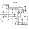
- FIGS. 1 and 2 With reference to Fig. 3 u. 4 The invention will now be described in more detail with reference to FIGS. 1 and 2.
- FIG. 1 in which the general principle of the transistor oscillator circuit according to the invention is shown, while FIG. 2 shows a particularly favorable embodiment in its details. Both versions can be implemented using bipolar transistors. In this context, however, it should be noted that both the oscillator and the mixing stage and the circuit parts to be used for the negative feedback on the oscillator can also be implemented using MOS technology.
- the two bipolar transistors T1 and T2 forming the oscillator in the circuit according to FIG. 1 are identical to one another and of the npn type. They are connected to their emitters and are connected via a resistor R1 to the second operating potential, which serves as a reference potential (ground) and is made available by a DC voltage source U1.
- the other pole of the DC voltage source U1 which supplies the first operating potential is connected to the collector of the transistor T1 or T2 of the oscillator via a resistor R7 or R8.
- the base of the transistor T1 forms the control input of the oscillator, since it is connected via a capacitor C1 to the frequency-determining control element of the oscillator.
- This tax body is either a pa parallel resonance circuit, i.e. a resonant circuit formed from a capacitor C with inductance L connected in parallel, which is on the one hand at the reference potential and on the other hand via the capacitor C1 at the control input T1 of the oscillator and via a further (same) capacitor C2 with the collector of the other transistor T2 Oscillator is connected.
- the resonant circuit can be serial. Then the inductance L is omitted at this point and the resonant circuit capacitor C is replaced by an inductor Ls exclusively connecting the two poles of the two coupling capacitors C1 and C2 facing away from the oscillator.
- the quartz crystal Q replaces the serial inductance Ls.
- the parallel inductance L and the parallel capacitor C are also omitted in this case.
- the base of transistor T1 is connected to the base of transistor T2 via two resistors R2 and R3 connected in series.
- the dividing point between these two resistors R2, R3 is connected to ground via the DC voltage source U3.
- Another capacitor C3 is provided between the base terminal of the second transistor T2 and the reference potential. Because of this feedback effect, which causes the oscillator effect of the differential amplifier T1, T2, between the base terminal of the transistor T1 and the collector terminal of the transistor T2, the collectors of the two transistors T1 and T2 are able to supply the subsequent mixer stage with the sine oscillations required to operate the circuit.
- the mixer stage consists of two pairs of transistors T3, T4 and T5, T6 which, like the transistors of the oscillator T1, T2, consist of transistors of the NPN type.
- the symmetrical mixing stage comes about because the Transistors T3 and T4 on the one hand and the transistors T5 and T6 on the other hand connected in pairs via their emitters and the collector of one transistor of the two pairs to the. an output terminal A1 and the collector of one of the two other transistors of the two pairs is connected to the other output terminal A2.
- the collector of transistor T3 and the collector of transistor T5 are at terminal A1
- the collector of transistor T4 and the collector of transistor T6 are at terminal A2 of the output of the mixer.
- the transistors T3 and T4 on the one hand and the transistors T5 and T6 on the other hand are combined into a pair via their emitters and each of the two pairs T3, T4 and T5, T6 via its emitters with the collector of a further npn transistor T7 or T8 connected.
- These transistors T7 and T8 are in turn combined by their emitters and connected via their emitters via a common resistor R4 to the common reference potential of the circuit.
- the transistors T3 and T6 form a first common input terminal via their base connections and the transistors T4 and T5 form a second common input terminal for the oscillator signal supplied by the oscillator output. Therefore, the base connections of transistors T3 and T6 are on the collector of transistor T1 and the base connections of transistors T4 and T5 of the mixer are on the collector of the other transistor T2 of the oscillator.
- the npn transistors T7 and T8 provided to act on the emitters of the first transistor pair T3, T4 on the one hand and of the second transistor pair T5, T6 of the mixer stage in turn serve as a signal input to the mixer stage and thus to the circuit. You are therefore in operation by an external signal, the z. B. is supplied by a (not shown) input amplifier, control For this purpose, the base of transistor T7 is connected to one input terminal E1 and the base of the other transistor'T8 to the other input terminal E2. Finally, the two transistors T7 and T8 provide the emitter potential required for the transistor pairs T3, T4 and T5, T6 of the mixer.
- a further DC voltage source U2 is provided, one pole of which is at the common reference potential, while the other pole is connected on the one hand to the base of the transistor T7 via a resistor R5 and to the base of the transistor T8 via a resistor R6.
- each of the two outputs of the oscillator that is, the collectors of the two transistors T1 and T2
- Resistor R9 and resistor R10 thus form a low-pass filter with capacitor C4, which is used to control one of the two inputs of the control amplifier.
- the signal output of the control amplifier V is located directly at the base of the transistor T2, which is not directly at the capacitor C1 and thus above it at the frequency-determining control element of the oscillator.
- the low-pass filter R9 and R10, C4 is dimensioned such that the appearance of the oscillator oscillation at the input of the control amplifier V is completely suppressed.
- the control amplifier V is expediently designed as an operational amplifier.
- the circuit of an oscillator-mixer combination in bipolar technology shown in FIG. 2 contains in principle the same circuit parts as are given in the circuit diagram according to FIG. 1. However, the circuit is much more detailed. It mainly consists of npn transistors and a few pnp transistors, as well as diodes, capacitors and resistors, so that, apart from the resonant circuit, the rest of the circuit can be easily summarized as monolithic. In addition to the circuit parts shown in FIG. 1, constant current sources serving, inter alia, to improve the desired effect and the operation of the oscillator and the mixing stage are provided.
- the resonant circuit designed in the example shown in FIG. 2 as a parallel resonant circuit and serving to fix the oscillator frequency is located above the two coupling capacitors 28 and 29 at the control input of the oscillator.
- the oscillator is in turn provided by two NPN transistors 33, 41, which correspond to transistors T1 and T2 according to FIG. 1 and are connected to their emitters.
- the resonant circuit 25 with its other connection at the reference potential (ground) lies with its first connection via the capacitor 28 on the collector of transistor 33 and via capacitor 29 at the base of transistor 41.
- the latter is also connected to the base of transistor 33 of the oscillator via a voltage divider consisting of the two resistors 68, 69.
- the dividing point of this voltage divider 68, 69 lies at the cathode of a diode 31, the anode of which is connected to the reference potential, that is to say ground.
- the cathode of the diode 31 is connected to the base of the transistor 33 and, on the other hand, via a resistor 30 to the output of a circuit part to be described and serving as a current source, while the anode of the diode 31 is at the reference potential.
- the collector of the oscillator transistor 33 and the collector of the oscillator transistor 41 are each via a resistor 34 or 38 am.Emitter each of a transistor 35 or 39 of the npn type, the collectors of which via a resistor 36 or 37 to that of a DC voltage source U1 delivered first operating potential are laid.
- the first operating potential is supplied by the positive terminal and the reference potential by the negative terminal of the DC voltage source U1.
- To generate the potential of the base connections of the two transistors 35 and 39 which serve to decouple the oscillator signal, these are connected via a resistor 40 to the positive pole of a further DC voltage source U4, which is also related to ground with its negative pole.
- the two cascode transistors 35 and 39 with their collectors form the two output connections of the oscillator.
- the emitters of the two oscillator transistors 33 and 41 are connected to the collector of an npn transistor 43, the emitter of which is combined with the emitter of two further transistors 44 and 45 (also of the npn type) also serving as current sources and over the collector-emitter path of a further npn transistor 54 and the resistor 55 is connected to the reference potential.
- the collector of the power supply transistor 44 is connected to the collector of the oscillator transistor 33 and the collector of the transistor 45 is connected to the collector of the oscillator transistor 41.
- the circuit means used to generate the base potentials of transistors 43, 44 and 45 will be discussed further below.
- the output connections of the oscillator that is to say the collectors of the npn transistors 35 and 39, are provided both for the feedback to be carried out according to the invention and for the loading of the mixing stage.
- the collector of transistor 35 is connected to the base of an npn transistor 120 and the collector of transistor 39 is connected to the base of an npn transistor 121.
- the collectors of these two transistors 120 and 121 are at the first operating potential, that is to say at the positive pole of the voltage source U1, and their emitter electrodes are each connected via a (similarly dimensioned) resistor 64 and 63, which in turn are connected to one another and connected to the reference potential of the circuit via a further resistor 24 are.
- the emitters of the two NPN transistors 120,. Serving as emitter followers for the mixing stage. 121 are connected to the inputs of the symmetrical mixer stage which are provided for the application by the oscillator.
- the mixer stage consists of the NPN transistors 107, 108, 109, 110, 111, 112 and 106 and 105, and the resistors 104, 122 and 123.
- the transistors 107 and 108 form the first transistor pair and the transistors 109 and 110 the second Transistor pair corresponding to the circuit shown in Fig. 1 for the balanced mixer.
- the combination of transistors 107 and 108 or 109 and 110 is in turn due to the connection of Emitters of the transistors of the relevant pair of transistors and their exposure to the collector of one npn transistor 106 or 105 assigned to the respective pair. As in FIG.
- transistors T7 and T8 are those which are to be processed externally via signal input 113
- Signal via their base connections to be controlled transistors 105 and 106 is also provided with the required base voltage by a further DC voltage source U2 via a resistor 122 and 123, respectively, while the emitters of these two transistors 105 and 106 are connected to the reference potential via a common resistor 104.
- the transistor 107 of the first and the transistor 110 of the second transistor pair of the mixer stage is controlled by the oscillator signal via the emitter of the transistor 120 operated as an emitter follower.
- transistor 108 of the first and transistor 109 of the second pair of the mixer stage are controlled by the emitter of transistor 121.
- the emitter of transistor 121 is also connected via a resistor 27 to the base of the circuit comprising transistors 11, which will be described below and 12.
- the collectors of transistor 107 and transistor 109 of the mixer stage jointly control the emitter of output transistor 111 (of the NPN type) and on the other hand the collectors of the two transistors 108 and 110 of the mixer stage jointly control the emitter of the second output transistor 112 (also of NPN type) ) the mixing level.
- the collectors of the two output transistors form the signal output 114 of the circuit.
- the base connections of the two output transistors 111 and 112 are connected together via the resistor 42 to the reference potential of the circuit.
- the collector of the oscillator transistor 33 is connected to the base of an npn transistor 70 and the collector of the oscillator transistor 41 is connected to the base of an npn transistor 73.
- the two last-mentioned transistors 70 and 73 are operated as emitter followers and are therefore with their collectors at the first operating potential supplied by the voltage source U1, while their emitters each have a resistor 71 and 72 (equally dimensioned) and a third - common - resistor 65 are at the reference potential of the circuit.
- the emitters of these two NPN transistors 70 and 73 are used to control two transistor combinations.
- the emitter of transistor 70 is connected on the one hand to the base of an npn transistor 67 and via a resistor 85 to the base of a further npn transistor 83, while the emitter of transistor 73 is connected to the base of an npn transistor 74 and above a resistor 84 is located at the base of the transistor 83 already mentioned.
- the npn transistor 83 is combined with a further npn transistor 82 to form a Darlington stage in that its emitter is directly connected to the base of the transistor 82 and its collector is connected to the collector of the transistor 82.
- the collectors of transistors 82, 83, 74 and 67 are at the first operating potential, that is, at the positive pole of U1.
- the emitters of the NPN transistors 67 and 74 are also connected to one another and are connected to the cathode of the diode 62 (which forms a capacitor), the anode of which is at the reference potential.
- the emitter of transistor 82 is connected to the base of a pnp transistor 86, the collector of which is connected to the reference potential and the emitter of which is connected to the cathode of a diode 87, the anode of which is connected to the base of a two-phase Collector pnp transistor 88 is connected.
- the one collector this transistor 88 is connected directly to the base of this transistor 88, the second collector of which is connected to the reference potential via the collector-emitter path of an npn transistor 96 and a resistor 98 connected to the emitter of this transistor 96.
- the emitter of the two-collector transistor 88 mentioned is connected on the one hand to the collector of a further pnp transistor 115 via a resistor 90 and to the emitter of a second pnp two-collector transistor 92 via a further resistor 91 which is the same as the resistor 90 .
- the connection of the two collectors and the base of the transistor 92 corresponds to the conditions in the two-collector transistor 88. Accordingly, the one collector and the base are connected directly to one another and are located on the anode of a diode 94, the cathode of which is connected to the emitter of a further pnp transistor 93.
- the collector of the last-mentioned pnp transistor 93 is at the reference potential.
- the second collector of the pnp transistor 92 is connected to the reference potential via the collector-emitter path of an npn transistor corresponding to the transistor 96 and a resistor 97 equal to the resistor 98. Both NPN transistors 95 and 96 form a base-coupled current source.
- the pnp transostor 115 mentioned in the last paragraph and intended to control the emitters of the two two-collector transostors 88 and 92 is connected with its emitter via a resistor 119 on the one hand to the first operating potential supplied by U1.
- the emitter of pnp transistor 116 is connected via resistor 118 to the first operating potential supplied by DC voltage source U1.
- the base of this further pnp transistor 116 is located across the resistor 117 both at the base of the pnp transistor 115 and on its own collector.
- the collector of the last presented PNP transistor 116 and therefore the base of the PNP transistor 115 are connected via the collector-emitter path of an npn - 100 connected transistor 99 and one connected to the emitter of this transistor 99 resistor to the reference potential of the circuit.
- the just introduced npn transistor 99 forms, together with another npn transistor 22, a constant current source.
- the collector of the npn transistor 22 is connected via a resistor 103 to the first operating potential supplied by U1 and with its emitter via the resistor 102 to the reference potential, while the base of the transistor 22 is connected via a resistor 101 to both its own collector and the Base of the npn transistor 99 is connected.
- the resistor 103 also serves to control the power supply of the oscillator transistors 33 and 41 in a manner to be described.
- the said collector of the two-collector pnp transistor 88 is located at the base of a pnp transistor 57 and via the resistor 59 at the positive pole of a further DC voltage source U3, which is already in connection with the control of the oscillator via the base connections of the transistors 33 and 41 connecting voltage divider 68, 69 was called.
- the pnp transistor 58 which is controlled by the collectors of the two-collector transistor 88 and the transistor 96, has its collector at the reference potential and its emitter at the base of a first npn transistor 57 and at the emitter of a further npn transistor 50.
- the collector of these two transistors 56 and 57 is at the first operating potential supplied by the DC voltage source U1.
- the transistor combination 56, 58 is used to clamp the maximum possible voltage at the base 57.
- the emitter of the npn transistor 57 is connected to the base of the npn transistors 44 and 45 already mentioned in connection with the oscillator transistors 33 and 41.
- the emitters of the npn transistors 70 and 73 provided at the input of the negative feedback branch of the oscillator and already mentioned are provided for controlling three npn transistors 67, 74 and 83.
- the emitters of the two transistors 67 and 74 are connected together and are connected to the cathode of a diode 62, the anode of which is held at the reference potential.
- Another diode 61 is also connected to the reference potential with the anode and to the base of the npn transistor 83 with the cathode and thus at the input of the Darlington stage composed of the transistors 82 and 83.
- the emitters of the two npn transistors 67 and 74 connected to the base of an npn transistor 66, the collector of which at the first operating potential (supplied by U1) and the emitter of the collector and emitter of a further npn transistor 75, and via a resistor 79 both at the base of the one already in connection with the second two Collector transistor 92 mentioned pnp transistor 93 and also via a further resistor 80 on the collector of a further npn transistor 77.
- the collector of the last-mentioned npn transistor 77 is also connected via a resistor 76 to the emitter of the npn transistor 75 connected as a diode.
- the emitter of the last introduced npn transistor 77 is connected to the reference potential via a resistor 78.
- the base of this transistor is already with the base of the in connection with the Darlington stage from the npn transistors 82, 83 introduced and their emitters for.
- Reference potential leading npn transistor 81 connected. Both basic connections are supplied via a fifth DC voltage source U5, the negative pole of which is at the operating potential.
- Another constant current source consists of the base-coupled npn transistors 3 and 4, the emitter of transistor 3 being connected directly and the emitter of transistor 5 being connected to the reference potential of the circuit via said resistor 5.
- the collector of the transistor 3 is connected to its own base and via a resistor 1 to the first operating potential.
- the collector of the second transistor 4 of the current source (ie its output) is connected to the collector of a further pnp transistor 6, the emitter of which is connected to the base of a further npn transistor 9 via a resistor 2 at the first operating potential and the base of which is connected via a resistor 7 is.
- a resistor 8 forms the connection of the emitter of this further npn transistor 9 to the first operating potential.
- the collector of the pnp transistor 9 is connected to the collector of two further npn transistors 11 and 12.
- the base of the first of these npn transistors leads via the resistor 26 to the base connection of the transistor 107 and to the base connection of the transistor 110 of the mixer stage and thus to the signal input to be applied to it by the oscillator.
- the base of the second of these npn transistors namely transistor 12, leads via resistor 27 to the base connections of transistors 108 and 109, and thus also to that input of the balanced mixer which is controlled by the other output of the oscillator.
- the base connections of the last introduced npn transistors 11 and 12 are bridged before the resistors 26 and 27 by two diodes which produce the desired low-pass effect.
- the base of the transistor 11 is connected to the anode of the diode 21 and the cathode of this diode 21 to the base of the npn transistor 12.
- the anode is directly connected to the base of the npn transistor 12 and the cathode to the pole of the base of the transistor 11.
- the collector terminals of the NPN transistors 11 and 12 are, as already mentioned, common to the q by the transistor 9, the transistors 3, 4, 6 and 9 containing constant current supplied ource.
- the signal output of the two npn transistors 11 and 12 is given by their emitter connections, which for this purpose are connected to the emitter of a pnp transistor 13 and 14, respectively.
- the base of the pnp transistor 13 and the pnp transistor 14 is connected directly to the collector of the power supply transistor 4 already mentioned.
- the collectors of the two last-mentioned pnp transistors 13 and 14 are located across the collector-emitter path of an npn transistor 17 or 18 and a resistor 19 or 16 connected upstream of the emitter of the relevant transistor 17 or 18 at the reference potential of the circuit.
- the two transistors 17 and 18 are directly connected to their base connections, the base of the transistor 18 also being short-circuited to its own collector, and so this transistor 18 is connected as a diode.
- the base of the two npn transistors 17 and 18 is connected to the anode of a diode 15, the cathode of which is connected to the collector of the npn transistor 17 and thus to the collector of the pnp transistor 13.
- the collectors of the transistors 17 and 13 via the already mentioned resistor 30 to the base of the oscillator sistor 33 and thus fed back to the oscillator.
- npn transistors 45 and 46 which have already been mentioned repeatedly in connection with the two oscillator transistors 33 and 41, receive their operating potential from the collector of an npn transistor 54, the emitter of which via a resistor 55, just like the emitter of the npn transistor 43, which has also already been presented is acted upon by the reference potential.
- Another npn transistor 52 is also connected to the reference potential with its emitter via the resistor 53, while its collector is connected on the one hand to the base of the above-mentioned npn transistor 44 or 45 and to the emitter of a further npn transistor 57 .
- the base connections of the three npn transistors 48, 52 and 54 are all connected to the collector of the power supply transistor 22 and thus also to the resistor 103, which establishes the connection to the first operating potential (DC voltage source U1) of the circuit.
- the npn transistor 46 also has its collector at the first operating potential, while the base potential of this transistor 46 is identical to the base potential of the pnp transistor 58 already mentioned in connection with the npn transistors 56 and 57 and the base potential of the now transistor 56 and is at the positive pole of the DC voltage source U3.
- the control amplifier in the feedback of the oscillator is through the input transistor 86, the diode 87, the two two-collector transistors 88 and 92, the diode 94 and the transistor 93, and the npn transistors 95 and 96 given.
- the input of the feedback is given by the two transistors 70 and 73.
- the opposite phase signal to the signal at the emitters of the two transistors 70 and 73 is generated by summation from the emitter of the two transistors 70 and 73 via the two resistors 84 and 85 to the base of the transistor 83. Residual components are grounded via the diode 61, so that the two resistors 84 and 85 in combination with the diode 61 act as a low pass.
- the reference value at the base of transistor 83 is obtained. This reference value is passed on via the emitter of transistor 83, the base of transistor 82 and the emitter of transistor 82 to the input transistor of the control amplifier, that is to say the base of pnp transistor 86.
- the antiphase signal at the emitters of transistors 70 and 73 is also routed to the base of transistors 67 and 74.
- the emitter of these transistors 67 and 74 is capacitively blocked against ground, that is to say the reference potential, via the diode 62 and is supplied with respect to the required emitter voltage from the base of the transistor 66. Thanks to the peak rectification of the transistors 67 and 74, an additional DC voltage potential is now formed on the diode 62 in accordance with the oscillator amplitude. This potential is passed on to the short-circuited base-collector path of transistor 75 via the emitter of transistor 66. The emitter of transistor 75 is supplied via resistor 76 from the collector of transistor 77 with the required operating current.
- the emitter of transistor 66 is connected to resistor 79.
- Resistor 80 goes from resistor 79 to the collector of transistor 77 and resistor 76 to the emitter of the transistor 75.
- the ratio of the resistance values in the dividers 79 and 80 sets a DC voltage value which is proportional to the voltage change at the emitters of the transistors 67 and 74. This gives the control amplifier its lead.
- the lead of the control amplifier is set via the voltage dividers 79 and 80 and thus also the oscillator amplitude.
- the output transistors 35 and 39 provided in the oscillator serve to ensure that the disturbances which originate from the input 113 of the mixer stage and which are present at the collector of these output transistors, as a result of the low collector-emitter reaction of the transistors 35, 39, are only greatly weakened on the Oscillator circuit can make noticeable.
- the signal at the base of the transistors 11 and 12 is amplified via the cascode stage 13 and 14 and the current mirror 17, 18.
- the diodes 31 and 15 serve to suppress control oscillations.
- the diodes 20 and 21 short-circuit the antiphase signal at the output of the resistors 26 and 27. This will. only the direct current component and at most components of very low frequency left to the control amplifier 11, 12.
- the control amplifier 86, 87 serves to control the oscillator amplitude via the push-pull current output, which is given by the collectors of the transistors 88 and 96, via the base of the transistor 57.
- the load resistor which sets the voltage is given by resistor 59.
- the control amplifier 11, 12 etc. on the other hand, has the task of reducing the asymmetry at the mixer.
- the further invention relates mainly to a further improvement of the transistor oscillator circuit described so far.
- the further invention also has advantages if it is applied to an oscillator circuit or quartz-controlled oscillator, which is provided by a feedback differential amplifier, even if the said oscillator is not intended to act on a mixer stage.
- the invention provides that the capacitor in the frequency-determining control element has its one connection to the first coupling capacitor leading to the first transistor of the differential amplifier and with. its second connection is directly connected to the second coupling capacitor leading to the collector of the second transistor of the differential amplifier, so that a further capacitor is provided in the frequency-determining control element in such a way that this further capacitor has one connection with that of the second Transistor of the differential amplifier facing away connection of the second coupling capacitor is connected directly and via a resistor to one pole of a third DC voltage source, while the other connection of this further capacitor in the frequency-determining controller n and the other pole of the third DC voltage source directly at the supply terminal of the reference potential Oscillator circuit lie.
- FIG. 3 A transistor oscillator circuit improved in this sense is shown in FIG. 3, while the oscillator circuit shown in FIG. 4 additionally corresponds to the previously described transistor oscillator circuit.
- the two bipolar transistors T1 and T2 forming the oscillator in the circuit according to FIGS. 3 and 4 are identical to one another and of the nph type. They are directly connected to their emitters and these emitters are connected via a common resistor R1 to the supply terminal of the circuit, ie to ground, which carries the reference potential.
- the supply terminal of the oscillator circuit which provides the first operating potential is connected to the positive pole, the terminal of the oscillator circuit which supplies the reference potential is connected directly to the negative pole of a first DC voltage source U1.
- the base of the first transistor T1 of the differential amplifier forms the one of the oscillator connected to the frequency-determining element, a first coupling capacitor C1 being provided between these two circuit parts.
- the above-mentioned frequency-determining control element is either a parallel resonance circuit (that is, it is formed from a capacitor with inductance connected in parallel ter resonant circuit), which is connected on the one hand to the supply terminal carrying the reference potential and on the other hand to the first coupling capacitor C1 leading to the base of the first transistor T1 of the differential amplifier.
- said control element can be provided by a serial resonant circuit. Then, the inductance L placed parallel to the resonant circuit capacitor in the circuits according to FIGS. 3 and 4 is replaced by an inductance which then forms the only connection between the connections of the two coupling capacitors C1 and C2 facing away from the transistors of the differential amplifiers T1 and T2. Finally, an inductance in the control element can be completely dispensed with and instead the two connections of a quartz oscillator capacitor can be connected to one of the two connections of the first and second coupling capacitors C1 and C2 not connected to one of the transistors T1 or T2. A particularly advantageous connection of the oscillating quartz capacitor is described further below as a further embodiment of an oscillator according to the invention.
- the base of the first transistor T1 of the differential amplifier is connected to the base of the second transistor T2 of the differential amplifier via two resistors R3 and R2 connected in series. s tärkers connected.
- the dividing point between these two resistors R2 and R3 is connected to the positive pole of the second DC voltage source according to the definition of the invention, that is to say the DC voltage source U3, while the other pole of this DC voltage source is connected to the supply terminal which carries the reference potential, that is to say the negative pole of the DC voltage source U1 , is created.
- Another capacitor C3 is provided between the base terminal of the second transistor T2 of the differential amplifier and the supply terminal carrying the reference potential.
- the collectors of these two oscillator transistors T1 and T2 are able to emit an undamped sine wave together. They accordingly form the two output terminals A1 * and A2 * of the oscillator according to FIG. 1.
- these two output terminals A1 and A2 are connected to two input transistors T3 and T6 of the mixer stage to be loaded.
- the series circuit of two capacitors C 'and C is provided in the control circuit of a transistor oscillator corresponding to the further invention instead of a single resonant circuit capacitor C as in the case of the disclosures of the main application.
- These two transistors C 'and C together form a capacitive voltage divider.
- the resonant circuit inductance L forms a connection between the two end connections of the voltage divider C ', C *, which bridges the two capacitors and bridges the divider point and also with one Connection at the supply terminal carrying the reference potential. In the case of a series resonant circuit this inductance L drops. Instead, an inductance bridging the two coupling capacitors C1 and C2 is provided. If the oscillator is to be controlled by a quartz oscillator instead, the capacitor containing the quartz oscillator takes the place of the inductance to be used if a series resonant circuit is used.
- the voltage divider formed from the two capacitors C 'and C is provided, the connection of this voltage divider to the two coupling capacitors C1 and C2, to the reference potential, to the resistor R and the DC voltage source U always that of FIGS. 1 and Fig. 2 apparent configuration corresponds.
- the second coupling capacitor C2 is provided by a quartz crystal.
- the free capacitor of the voltage divider C ' is connected with its free connection to the first coupling capacitor C1 and, via this, to the base of the first oscillator transistor T1.
- the free capacitor of the second capacitor C * of the capacitive voltage divider is connected to the supply terminal carrying the reference potential, to which the negative pole of the third DC voltage source U * is also connected.
- the positive pole of the third DC voltage source U * is via the resistor R according to the definition of the invention on the one hand with the dividing point, i.e. a circuit point between the two capacitors C 'and C * of the capacitive voltage divider and on the other hand with the connection of the second coupling capacitor C2 facing away from T2 connected.
- the circuit inductance L is at the end connections of the capacitive voltage divider C ', C *.
- the previously customary and constructed using a differential amplifier T1, T2 are so-called two-point oscillators, in which the base of the one transistor T1 is galvanically or capacitively connected to the collector of the second transistor T2 of the differential amplifier.
- the center point of this connection lies at the high point of a parallel resonant circuit or at the intermediate point of a series resonant resonant circuit.
- the negative steepness of the admittance curve of these coupling points ensures that the oscillation at the output of the oscillator is retained.
- the blind components of this slope lead both to an annoying frequency drift and to a reduction in the tuning range.
- the finite gain from the base of the second transistor T2 of the differential amplifier to the output of the amplifier at the collector of the transistor T2 is not always sufficient to maintain the oscillation state.
- an oscillating circuit or oscillating-gauze control circuit controlling the input of such an oscillator is equipped with a series capacitance C ', C * instead of a simple capacitor C and the high point or midpoint of such an oscillating circuit or quartz control circuit corresponding to that of Coupled with the invention given proposals to the oscillator transistors T1 and T2, the parasitic capacitive and real portion of the active circuit in the overall resonant circuit or quartz control circuit is significantly reduced. This increases the frequency variation range, increases vibration security and drastically reduces the tendency to frequency drift.
- the capacitor C 'of the capacitive voltage divider C', C in the form of a, which is located on the first coupling capacitor C1 Realize capacitance diode.
- the other capacitor C can also be provided by a capacitance diode, which is recommended, for example, for the cable television sector or for the FM region.
- the capacitance of the two capacitors C 'and C can be influenced by means of the potential supplied by the third direct voltage source U and applied to the resistor R, in particular if at least one of these two capacitors is provided by a semiconductor capacitance diode, ie a varactor diode or a normal pn junction diode.
- the influencing of the capacitances C 'and C has an advantageous effect on the setting range for the oscillation frequency.
- the first coupling capacitor C1 can also be connected in series with a further capacitance diode, which is then expediently used between the coupling capacitor C1 and the first capacitor C 'of the capacitive voltage divider C', C.
- the coupling capacitor C2 leading to the collector of the second transistor of the differential amplifier can be replaced by an oscillating quartz crystal, so that the circuit for an oscillator controlled oscillator according to the invention can be somewhat simplified in this way.
- This also eliminates the direct connection between the two coupling capacitors C1 and C2, which is present in the other case of the circuit described above when using a quartz crystal control. This leads to a so-called overtone oscillator.
- the symmetrical mixer stage arises because the npn transistors T3 and T4 on the one hand and the npn transistors T5 and T6 on the other hand are connected in pairs via their emitters and the collector of a transistor of the two pairs to the one output terminal A1 and the One of the two other transistors of the two pairs is connected to the other output terminal A2.
- the col detector of transistor T3 and the collector of transistor T5 at terminal A1 the collector of transistor -T4 and the collector of transistor T6 at terminal A2 of the output of the mixer.
- the transistors T3 and T6 as well as the transistors T5 and T4 are combined to form a pair of transistors via their base connections, in that the two transistors T3 and T6 together from the collector of the first oscillator transistor T1 and the two transistors T4 and T5 together from the collector of the second oscillator transistor T2 can be controlled via their basic connections.
- the emitters of transistors T3 and T4 are connected to the collector of a further npn transistor T7 and the emitters of transistors T5 and T6 are connected to the collector of a sixth npn transistor of the mixing stage, which is designated T8.
- the emitters of the two last-mentioned npn transistors T7 and T8 are connected to the reference potential via a common emitter series resistor, that is to say to the supply terminal for the reference potential defined above.
- the emitter series resistor of T7 and T8 is resistor R4.
- a fourth DC voltage source U2 lies with its nega-pole at said power supply terminal for the B ezugspo- tential and with its positive pole via a resistor R5 or R6 to the base of transistor T7 unddes transistor T8.
- the base connections of the two transistors T7 and T8 each form a connection E1, E2 to be processed jointly by an external signal to be processed, for example via a preamplifier (not shown), that is to say maW, the signal input of the mixing stage.
- each of the two output terminals A1, A2 * of the oscillator that is, the collector of the oscillator transistor T1 and T2, via a resistor R9 or R10 to each input of a control amplifier V.
- the two resistors R9 and R10 are connected to one another at the connection facing away from the transistor T1 and T2 via a capacitor C4.
- the resistor R9 and the resistor R10 thus form a low-pass filter with the capacitor C4, through which the control amplifier V is controlled.
- the signal output of the control amplifier V is located directly at the base of the second oscillator transistor T2.
- the low-pass filter R9, R10, C4 is dimensioned so that the occurrence of the oscillator oscillation at the input of the control amplifier V is completely suppressed. This leads to the negative feedback leading via the control amplifier V becoming purely direct current. The consequence of this is that the inevitably inevitable asymmetry of the potential changes at the two output terminals A1, A2 * of the oscillator is reduced. This has the effect of suppressing the oscillator noise and compensating for further interference originating from the oscillator on the IF signal supplied by the output A1, A2 of the mixer stage.
- the capacitor C provided there in the resonant circuit 25 as a voltage divider from two series-connected capacitors C ', C * and this - together with another DC voltage source corresponding to the DC voltage 1 and 2 of the present application to the capacitor 28 which corresponds to the first coupling capacitor C1 and to the capacitor 29 which corresponds to the second coupling capacitor C2.
Abstract
Mit Hilfe des rückgekoppelten Differenzverstärkers (T1, T2) ist ein schwingkreis- oder quarzgesteuerter Oszillator aufgebaut, der eine symmetrische Mischstufe (T3 bis T8) ansteuert. Der Ausgang des Oszillators führt im Sinne einer Gegenkopplung über einen Tiefpass (R9,R10,C4) und einen Gleichstromverstärker (V) an seinen Eingang zurück. Diese Maßnahme dient der Unterdrückung einer störenden Einwirkung des Signales vom Oszillator auf die Mischstufe. Außerdem wird eine stärkere Unterdrückung des Oszillatorrauschens als bei den herkömmlichen Schaltungen erreicht. Wenn man zusätzlich den Kondensator (C) im frequenzbestimmenden Steuerorgan mit seinem einen Anschluß an den ersten Transistor (T1) über einen zu dessen Basis führenden ersten Koppelkondensator (C1) und an den zweiten Transistor (T2) des Oszillators über einen zu dessen Kollektor führenden zweiten Koppelkondensator (C2) anlegt und außerdem dafür sorgt, daß der besagte Kondensator (C) mit dem zuletzt genannten Anschluß einerseits über einen Kondensator (C2) und andererseits über einen Widerstand (R8) und eine mit diesem in Serie liegende Gleichspannungsquelle (U1) an das Bezugspotential der Oszillatorschaltung legt, so erhält man eine weitere Verbesserung hinsichtlich der Schwingsicherheit, des Durchstimmbereiches und der Frequenzdrift.With the help of the feedback differential amplifier (T1, T2) an oscillator or quartz-controlled oscillator is set up, which controls a symmetrical mixer stage (T3 to T8). The output of the oscillator leads back to its input in the sense of negative feedback via a low pass (R9, R10, C4) and a direct current amplifier (V). This measure serves to suppress a disturbing effect of the signal from the oscillator on the mixer stage. In addition, more suppression of the oscillator noise is achieved than with the conventional circuits. If you additionally the capacitor (C) in the frequency-determining control element with its one connection to the first transistor (T1) via a first coupling capacitor (C1) leading to its base and to the second transistor (T2) of the oscillator via a second leading to its collector Coupling capacitor (C2) creates and also ensures that said capacitor (C) with the last-mentioned connection on the one hand via a capacitor (C2) and on the other hand via a resistor (R8) and a direct voltage source (U1) connected in series with this to the Reference potential of the oscillator circuit sets, so you get a further improvement in terms of vibration safety, the tuning range and the frequency drift.
Description
Die Erfindung betrifft eine Transistor-Oszillatorschaltung, bei der der schwingkreis- bzw. quarzgesteuerte Oszillator durch einen rückgekoppelten Differenzverstärker gegeben und zur Beaufschlagung einer Mischstufe vorgesehen ist.The invention relates to a transistor oscillator circuit, in which the oscillating circuit or quartz-controlled oscillator is provided by a feedback differential amplifier and is provided to act on a mixer stage.
Solche Schaltungen lassen sich z. B. in der Rundfunk- bzw. in der Fernsehtechnik einsetzen. Einzelheiten hinsichtlich des Aufbaus von auf der Grundlage eines Differenzverstärkers liegenden Oszillatoren in Bipolartechnik sind z. B. aus "Funkschau" (1971), H. 15, S. 465 und 466 bekannt. Solche Oszillatoren sind sowohl für den Betrieb mit parallel- als auch mit seriell aufgebauten Schwingkreisen geeignet und arbeiten trotz ihres einfachen Aufbaus selbst bei stark unterschiedlichen Resonanzwiderständen einwandfrei ohne daß es zur Entstehung von Kippschwingungen.kommt. Außerdem ist die Amplitude am Schwingkreis stabilisiert und die Schaltung weitgehend monolithisch zusammenfaßbar. Verwendet man jedoch den Oszillator zur Beaufschlagung einer Mischstufe insbesondere in einer integrierten Oszillator-Tuner-Mischerschaltung, so wird bei Anwendung der üblichen Schal tungsweisen bei weitem nicht das Optimum hinsichtlich der Unterdrückung der Wirkung des Eingangssignals bzw. Oszillatorsignals auf den Ausgang der Mischstufe und damit auf die Wiedergabecualität des eine solche Schaltung verwendenden Rundfunk- oder Fernsehempfängers erreicht. Auch hinsichtlich der Unterdrückung des Oszillatorrauschens sind die bekannten Schaltungen dieser Art verbesserungsbedürftig. Hier greife nun die vorliegende Erfindung ein.Such circuits can e.g. B. use in radio or television technology. Details regarding the construction of oscillators based on a differential amplifier in bipolar technology are, for. B. from "Funkschau" (1971), H. 15, pp 465 and 466 known. Such oscillators are suitable for operation with both parallel and serial resonant circuits and, despite their simple structure, work perfectly even with very different resonance resistances without the occurrence of tilting vibrations. In addition, the amplitude at the resonant circuit is stabilized and the circuit can be summarized largely monolithically. However, if the oscillator is used to apply a mixing stage, in particular in an integrated oscillator-tuner-mixer circuit, when using the conventional switching methods, the optimum in terms of suppressing the effect of the input signal or oscillator signal on the output of the mixing stage and thus on is far from being optimal achieves the reproduction quality of the radio or television receiver using such a circuit. The known circuits of this type are also in need of improvement with regard to the suppression of oscillator noise. The present invention intervenes here.
Die Erfindung sieht zur Verbesserung einer Transistor-0szillatorschaltung der eingangs definierten Art vor, daß der stromführende Ausgang der beiden den Oszillator bildenden Transistoren sowohl an je einen Eingangsanschluß der symmetrisch ausgebildeten Mischstufe als auch über je einen Tiefpaß an je einen Eingang eines gemeinsamen Regelverstärkers gelegt und der Ausgang dieses Regelverstärkers auf den Oszillator im Sinne einer Gegenkopplung rückgekoppelt ist. und eine weitere AusgestaltungIn order to improve a transistor oscillator circuit of the type defined in the introduction, the invention provides that the current-carrying output of the two transistors forming the oscillator is connected both to an input terminal of the symmetrically designed mixing stage and via a low-pass filter to an input of a common control amplifier and the Output of this control amplifier is fed back to the oscillator in the sense of negative feedback. and a further embodiment
- an Hand der Fig. 3 u. 4 Die Erfindung wird nun anhand der Figuren 1 und 2 näher beschrieben. Zunächst wird auf Fig. 1 Bezug genommen, in der das allgemeine Prinzip der erfindungsgemäßen Transistor-Oszillatorschaltung dargestellt ist, während in Fig. 2 eine besonders günstige Ausgestaltung in ihren Details gezeigt ist. Die beiden Ausführungen sind mittels-Bipolartransistoren zu realisieren. Zu bemerken ist jedoch in diesem Zusammenhang, daß sowohl der Oszillator, als auch die Mischstufe und die für die Gegenkopplung auf den Oszillator einzusetzenden Schaltungsteile sich auch in MOS-Technik realisieren lassen.- With reference to Fig. 3 u. 4 The invention will now be described in more detail with reference to FIGS. 1 and 2. First, reference is made to FIG. 1, in which the general principle of the transistor oscillator circuit according to the invention is shown, while FIG. 2 shows a particularly favorable embodiment in its details. Both versions can be implemented using bipolar transistors. In this context, however, it should be noted that both the oscillator and the mixing stage and the circuit parts to be used for the negative feedback on the oscillator can also be implemented using MOS technology.
Die beiden den Oszillator bei der Schaltung gemäß Fig. 1 bildenden Bipolartransistoren T1 und T2 sind einander gleich und vom npn-Typ. Sie sind mit ihren Emittern verbunden und über einen Widerstand R1 an das als Bezugspotential (Masse) dienende zweite Betriebspotential gelegt, das von einer Gleichspannungsquelle U1 zur Verfügung gestellt ist. Der das erste Betriebspotential liefernde andere Pol der Gleichspannungsquelle U1 liegt über je einen Widerstand R7 bzw. R8 am Kollektor des Transistors T1 bzw. T2 des Oszillators.The two bipolar transistors T1 and T2 forming the oscillator in the circuit according to FIG. 1 are identical to one another and of the npn type. They are connected to their emitters and are connected via a resistor R1 to the second operating potential, which serves as a reference potential (ground) and is made available by a DC voltage source U1. The other pole of the DC voltage source U1 which supplies the first operating potential is connected to the collector of the transistor T1 or T2 of the oscillator via a resistor R7 or R8.
Die Basis des Transistors T1 bildet den Steuereingang des Oszillators, da er über einen Kondensator C1 an das frequenzbestimmende Steuerorgan des Oszillators angeschlossen ist. Dieses Steuerorgan ist entweder ein Parallel-Resonanzkreis, also ein aus einem Kondensator C mit parallelgeschalteter Induktivität L gebildeter Schwingkreis, der einerseits am Bezugspotential und andererseits über den Kondensator C1 am Steuereingang T1 des Oszillators liegt sowie über einen weiteren (gleichen) Kondensator C2 mit dem Kollektor des anderen Transistors T2 des Oszillators verbunden ist.The base of the transistor T1 forms the control input of the oscillator, since it is connected via a capacitor C1 to the frequency-determining control element of the oscillator. This tax body is either a pa parallel resonance circuit, i.e. a resonant circuit formed from a capacitor C with inductance L connected in parallel, which is on the one hand at the reference potential and on the other hand via the capacitor C1 at the control input T1 of the oscillator and via a further (same) capacitor C2 with the collector of the other transistor T2 Oscillator is connected.
In Alternative hierzu kann der Schwingkreis seriell sein. Dann entfällt die Induktivität L an dieser Stelle und der Schwingkreiskondensator C wird durch eine,die beiden- dem Oszillator abgewandten Pole der beiden Koppelkondensatoren C1 und C2 ausschließlich verbindende Induktivität Ls ersetzt. Bei einer Quarzsteuerung ersetzt der Schwingquarz Q die serielle Induktivität Ls. Die Parallelinduktivität L und der Parallelkondensator C entfallen in diesem Falle ebenfalls.Alternatively, the resonant circuit can be serial. Then the inductance L is omitted at this point and the resonant circuit capacitor C is replaced by an inductor Ls exclusively connecting the two poles of the two coupling capacitors C1 and C2 facing away from the oscillator. In the case of a quartz control, the quartz crystal Q replaces the serial inductance Ls. The parallel inductance L and the parallel capacitor C are also omitted in this case.
Die Basis des Transistors T1 ist mit der Basis des Transistors T2 über zwei hintereinandergeschaltete Widerstände R2 und R3 verbunden. Der Teilerpunkt zwischen diesen beiden Widerständen R2, R3 ist über die Gleichspannungsquelle U3 mit Masse verbunden. Ein weiterer Kondensator C3 ist zwischen dem Basisanschluß des zweiten Transistors T2 und dem Bezugspotential vorgesehen. Aufgrund dieser die Oszillatorwirkung des Differenzverstärkers T1, T2 bewirkenden Rückkopplung zwischen dem BasisanschluB des Transistors T1 und dem Kollektoranschluß des Transistors T2 sind die Kollektoren der beiden Transistoren T1 und T2 imstande, die nachfolgende Mischstufe mit den zum Betrieb der Schaltung erforderlichen Sinusschwingungen zu versorgen.The base of transistor T1 is connected to the base of transistor T2 via two resistors R2 and R3 connected in series. The dividing point between these two resistors R2, R3 is connected to ground via the DC voltage source U3. Another capacitor C3 is provided between the base terminal of the second transistor T2 and the reference potential. Because of this feedback effect, which causes the oscillator effect of the differential amplifier T1, T2, between the base terminal of the transistor T1 and the collector terminal of the transistor T2, the collectors of the two transistors T1 and T2 are able to supply the subsequent mixer stage with the sine oscillations required to operate the circuit.
Die Mischstufe besteht aus zwei Transistorpaaren T3, T4 und T5, T6, die ebenso wie die Transistoren des Oszillators T1, T2 aus Transistoren vom npn-Typ bestehen. Die symmetrische Mischstufe kommt dadurch zustande, daß die Transistoren T3 und T4 einerseits und die Transistoren T5 und T6 andererseits über ihre Emitter paarweise miteinander verbunden und der Kollektor je eines Transistors der beiden Paare an die. eine Ausgangsklemme A1 und der Kollektor je eines der beiden anderen Transistoren der beiden Paare an die andere Ausgangsklemme A2 gelegt ist. Im gezeichneten Beispielsfall liegt der Kollektor des Transistors T3 und der Kollektor des Transistors T5 an der Klemme A1, der Kollektor des Transistors T4 und der Kollektor des Transistors T6 an der Klemme A2 des Ausgangs der Mischstufe.The mixer stage consists of two pairs of transistors T3, T4 and T5, T6 which, like the transistors of the oscillator T1, T2, consist of transistors of the NPN type. The symmetrical mixing stage comes about because the Transistors T3 and T4 on the one hand and the transistors T5 and T6 on the other hand connected in pairs via their emitters and the collector of one transistor of the two pairs to the. an output terminal A1 and the collector of one of the two other transistors of the two pairs is connected to the other output terminal A2. In the example shown, the collector of transistor T3 and the collector of transistor T5 are at terminal A1, the collector of transistor T4 and the collector of transistor T6 are at terminal A2 of the output of the mixer.
Andererseits sind die Transistoren T3 und T4 einerseits und die Transistoren T5 und T6 andererseits über ihre Emitter zu jeweils einem Paar zusammengefaßt und jedes der beiden Paare T3, T4 und T5, T6 über seine Emitter mit dem Kollektor je eines weiteren npn-Transistors T7 bzw. T8 verbunden. Diese Transistoren T7 und T8 sind ihrerseits wiederum über ihre Emitter zusammengefaßt und über ihre Emitter über einen gemeinsamen Widerstand R4 am gemeinsamen Bezugspotential der Schaltung angeschaltet. Die Transistoren T3 und T6 bilden über ihre Basisanschlüsse eine erste gemeinsame Eingangsklemme und die Transistoren T4 und T5 eine zweite gemeinsame Eingangsklemme für das vom Oszillatorausgang gelieferte Oszillatorsignal. Deshalb liegen die Basisanschlüsse der Transistoren T3 und T6 am Kollektor des Transistors T1 und die Basisanschlüsse der Transistoren T4 und T5 der Mischstufe am Kollektor des anderen Transistors T2 des Oszillators.On the other hand, the transistors T3 and T4 on the one hand and the transistors T5 and T6 on the other hand are combined into a pair via their emitters and each of the two pairs T3, T4 and T5, T6 via its emitters with the collector of a further npn transistor T7 or T8 connected. These transistors T7 and T8 are in turn combined by their emitters and connected via their emitters via a common resistor R4 to the common reference potential of the circuit. The transistors T3 and T6 form a first common input terminal via their base connections and the transistors T4 and T5 form a second common input terminal for the oscillator signal supplied by the oscillator output. Therefore, the base connections of transistors T3 and T6 are on the collector of transistor T1 and the base connections of transistors T4 and T5 of the mixer are on the collector of the other transistor T2 of the oscillator.
Die zur Beaufschlagung der Emitter des ersten Transistorpaares T3, T4 einerseits und des zweiten Transistorpaares T5, T6 der Mischstufe vorgesehenen npn-Transistoren T7 und T8 dienen ihrerseits als Signaleingang der Mischstufe und damit der Schaltung. Sie werden deshalb im Betrieb durch ein externes Signal, das z. B. von einem (nicht dargestellten) Eingangsverstärker geliefert wird, gesteuert. Hierzu ist die Basis des Transistors T7 mit der einen Eingangsklemme E1 und die Basis des anderen Transistors'T8 mit der anderen Eingangsklemme E2 verbunden. Schließlich liefern die beiden Transistoren T7 und T8 das für die Transistorpaare T3, T4 und T5, T6 der Mischstufe erforderliche Emitterpotential. Hierzu ist eine weitere Gleichspannungsquelle U2 vorgesehen, deren einer Pol auf dem gemeinsamen Bezugspotential liegt, während der andere Pol einerseits über einen Widerstand R5 an die Basis des Transistors T7 und über einen Widerstand R6 andererseits an die Basis des Transistors T8 gelegt ist.The npn transistors T7 and T8 provided to act on the emitters of the first transistor pair T3, T4 on the one hand and of the second transistor pair T5, T6 of the mixer stage in turn serve as a signal input to the mixer stage and thus to the circuit. You are therefore in operation by an external signal, the z. B. is supplied by a (not shown) input amplifier, control For this purpose, the base of transistor T7 is connected to one input terminal E1 and the base of the other transistor'T8 to the other input terminal E2. Finally, the two transistors T7 and T8 provide the emitter potential required for the transistor pairs T3, T4 and T5, T6 of the mixer. For this purpose, a further DC voltage source U2 is provided, one pole of which is at the common reference potential, while the other pole is connected on the one hand to the base of the transistor T7 via a resistor R5 and to the base of the transistor T8 via a resistor R6.
Wesentlich für die Erfindung ist nun, daß jeder der beiden Ausgänge des Oszillators, also die Kollektoren der beiden Transistoren T1 und T2, über je einen Widerstand R9 bzw. R10an je einen Eingang eines Regelverstärkers V, also eines Differenzverstärkers, gelegt und außerdem der dem Transistor T1 bzw. T2 abgewandte Anschluß des Widerstands R9 bzw. R10über einen Kondensator C4 verbunden ist. Damit bildet der Widerstand R9 und der Widerstand R10mit dem Kondensator C4 einen Tiefpaß, der zur Steuerung je eines der beiden Eingänge des Regelverstärkers dient.It is essential for the invention that each of the two outputs of the oscillator, that is, the collectors of the two transistors T1 and T2, each have an input of a control amplifier V, that is to say a differential amplifier, via a resistor R9 and R10, and also that of the transistor Connection of resistor R9 or R10 facing away from T1 or T2 is connected via a capacitor C4. Resistor R9 and resistor R10 thus form a low-pass filter with capacitor C4, which is used to control one of the two inputs of the control amplifier.
Der Signalausgang des Regelverstärkers V liegt unmittelbar an der Basis des nicht unmittelbar an dem Kondensator C1 und damit über diesem an dem frequenzbestimmenden Steuerorgan des Oszillators liegenden Transistors T2.The signal output of the control amplifier V is located directly at the base of the transistor T2, which is not directly at the capacitor C1 and thus above it at the frequency-determining control element of the oscillator.
Der Tiefpaß R9 und R10,C4 wird so dimensioniert, daß das Erscheinen der Oszillatorschwingung am Eingang des Regelverstärkers V völlig unterdrückt wird. Dies bedingt, daß die Gegenkopplung, die durch die beschriebene Schaltung bewirkt wird, rein gleichstrommäßig ist. Die Folge davon ist, daß die im Prinzip unvermeidbare Unsymmetrie der Potentialänderungen an den beiden Ausgangsklemmen des Oszillators und damit an den beiden Eingängen T3, T6 und T4, T5 vermindert wird. Dies wirkt sich im Sinne einer Unterdrückung des Oszillatorrauschens sowie einer Kompensation weiterer vom Oszillator herrührender Störungen auf das vom Ausgang der Mischstufe A1, A2 gelieferte ZF-Signal aus, so daß die vorgesehene Gegenkopplung am Oszillator einwandfrei eine erhebliche Verbesserung im Vergleich zu Schaltungen bedeutet, die die der Erfindung entsprechende Maßnahme nicht verwenden.The low-pass filter R9 and R10, C4 is dimensioned such that the appearance of the oscillator oscillation at the input of the control amplifier V is completely suppressed. This means that the negative feedback caused by the circuit described is purely direct current. The consequence of this is that the inevitably inevitable asymmetry of the potential changes at the two output terminals of the oscillator and thus at the two inputs T3, T6 and T4, T5 is reduced. This has the effect of suppressing the oscillator noise and compensating for further interference originating from the oscillator on the IF signal supplied by the output of the mixer stage A1, A2, so that the negative feedback provided on the oscillator perfectly means a significant improvement compared to circuits which do not use the measure corresponding to the invention.
Der Regelverstärker V ist zweckmäßig als Operationsverstärker ausgebildet.The control amplifier V is expediently designed as an operational amplifier.
Die in Fig. 2 dargestellte Schaltung einer Oszillator-Mischer-Kombination in Bipolartechnik enthält im Prinzip dieselben Schaltungsteile, wie sie in dem Schaltbild gemäß Fig. 1 angegeben sind. Jedoch ist die Schaltung wesentlich detaillierter. Sie besteht in der Hauptsache aus npn-Transistoren nebst einigen pnp-Transistoren, sowie aus Dioden, Kapazitäten und Widerständen, so daß, wenn man vom Schwingkreis absieht, die übrige Schaltung sich ohne weiteres monolithisch zusammenfassen läßt. Zusätzlich zu den aus Fig. 1 ersichtlichen Schaltungsteilen sind unter anderem der Verbesserung der angestrebten Wirkung sowie des Betriebs des Oszillators und der Mischstufe dienende Konstantstromquellen vorgesehen.The circuit of an oscillator-mixer combination in bipolar technology shown in FIG. 2 contains in principle the same circuit parts as are given in the circuit diagram according to FIG. 1. However, the circuit is much more detailed. It mainly consists of npn transistors and a few pnp transistors, as well as diodes, capacitors and resistors, so that, apart from the resonant circuit, the rest of the circuit can be easily summarized as monolithic. In addition to the circuit parts shown in FIG. 1, constant current sources serving, inter alia, to improve the desired effect and the operation of the oscillator and the mixing stage are provided.
Der in dem in Fig. 2 gezeichneten Beispielsfall als Parallelschwingkreis ausgebildete und der Festlegung der Oszillatorfrequenz dienende Schwingkreis liegt über den beiden Koppelkondensatoren 28 und 29 an dem Steuereingang des Oszillators. Der Oszillator ist wiederum durch zwei npn-Transistoren 33, 41 gegeben, die den Transistoren T1 und T2 gemäß Fig. 1 entsprechen und mit ihren Emittern verbunden sind. Der mit seinem anderen Anschluß am Bezugspotential (Masse) liegende Schwingkreis 25 liegt mit seinen ersten Anschluß über den Kondensator 28 am Kollektor des Transistors 33 und über den Kondensator 29 an der Basis des Transistors 41. Dieser ist außerdem über einen aus den beiden Widerständen 68, 69 bestehenden Spannungsteiler mit der Basis des Transistors 33 des Oszillators verbunden. Der Teilerpunkt dieses Spannungsteilers 68, 69 liegt an der Kathode einer Diode 31, deren Anode mit dem Bezugspotential, also Masse, verbunden ist. Außerdem ist die Kathode der Diode 31 mit der Basis des Transistors 33 und andererseits über einen Widerstand 30 an den Ausgang eines noch zu beschreibenden und als Stromquelle dienenden Schaltungsteils gelegt, während die Anode der Diode 31 am Bezugspotential liegt.The resonant circuit designed in the example shown in FIG. 2 as a parallel resonant circuit and serving to fix the oscillator frequency is located above the two
Der Kollektor des Oszillatortransistors 33 sowie der Kollektor des Oszillatortransistors 41 liegt über je einen Widerstand 34 bzw. 38 am.Emitter je eines Transistors 35 bzw. 39 vom npn-Typ, deren Kollektoren über je einen Widerstand 36 bzw. 37 an das von einer Gleichspannungsquelle U1 gelieferte erste Betriebspotential gelegt sind. Das erste Betriebspotential wird von der positiven Klemme und das Bezugspotential von der negativen Klemme der Gleichspannungsquelle U1 geliefert. Für die Erzeugung des Potentials der Basisanschlüsse der beiden der Signalentkopplung des Oszillatorsignals dienenden Transistoren 35 und 39 sind diese über einen Widerstand 40 an den positiven Pol einer weiteren Gleichspannungsquelle U4 gelegt, die mit ihrem negativen Pol ebenfalls auf Masse bezogen ist. Die beiden Kaskodetransistoren 35 und 39 bilden mit ihren Kollektoren die beiden Ausgangsanschlüsse des Oszillators.The collector of the
Um den Oszillator auch an das Bezugspotential anzuschließen sind die Emitter der beiden Oszillatortransistoren 33 und 41 an den Kollektor eines npn-Transistors 43 gelegt, dessen Emitter mit dem Emitter zweier weiterer ebenfalls als Stromquelle dienender Transistoren 44 und 45 (ebenfalls vom npn-Typ) zusammengefaßt und über die Kollektor-Emitterstrecke eines weiteren npn-Transistors 54 und den Widerstand 55 an das Bezugspotential gelegt ist. Dabei ist der Kollektor des Stromversorgungstransistors 44 mit dem Kollektor des Oszillatortransistors 33 und der Kollektor des Transistors 45 mit dem Kollektor des Oszillatortransistors 41 verbunden. Auf die der Erzeugung der Basispotentiale der Transistoren 43, 44 und 45 dienenden Schaltungsmittel wird weiter unten noch eingegangen.In order to also connect the oscillator to the reference potential, the emitters of the two
Die Ausgangsanschlüsse des Oszillators, also die Kollektoren der npn-Transistoren 35 und 39 sind sowohl für die gemäß der Erfindung vorzunehmende Rückkopplung als auch für die Beaufschlagung der Mischstufe vorgesehen. Zu diesem Zweck ist der Kollektor des Transistors 35 mit der Basis eines npn-Transistors 120 und der Kollektor des Transistors 39 mit der Basis eines npn-Transistors 121 verbunden. Die Kollektoren dieser beiden Transistoren 120 und 121 liegen am ersten Betriebspotential, also am positiven Pol der Spannungsquelle U1 und ihre Emitterelektroden über je einen (gleichbemessenen) Widerstand 64 und 63, die ihrerseits miteinander verbunden und über einen weiteren Widerstand 24 an das Bezugspotential der Schaltung gelegt sind. Die Emitter der beiden als Emitterfolger für die Mischstufe dienenden npn-Transistoren 120,. 121 sind an die für die Beaufschlagung durch den Oszillator vorgesehenen Eingänge der symmetrischen Mischstufe gelegt.The output connections of the oscillator, that is to say the collectors of the
Die Mischstufe besteht aus den npn-Transistoren 107, 108, 109, 110, 111, 112 und 106 und 105, sowie den Widerständen 104, 122 und 123. Die Transistoren 107 und 108 bilden das erste Transistorpaar und die Transistoren 109 und 110 das zweite Transistorpaar entsprechend der in Fig. 1 gebrachten Schaltung für die symmetrische Mischstufe. Die Zusammenfassung der Transistoren 107 und 108 bzw. 109 und 110 ist wiederum durch die Verbindung der Emitter der Transistoren des betreffenden Transistorpaares sowie deren Beaufschlagung durch den Kollektor je eines dem betreffenden Paar zugeordneten npn-Transistors 106 bzw. 105. Ebenso wie in Fig. 1 die Transistoren T7 und T8 sind die durch das extern über den Signaleingang 113 mit dem zu verarbeitenden Signal über ihre Basisanschlüsse zu steuernden Transistoren 105 und 106 außerdem durch eine weitere Gleichspannungsquelle U2 über je einen Widerstand 122 bzw. 123 mit der erforderlichen Basisspannung versehen, während die Emitter dieser beiden Transistoren 105 und 106 über einen gemeinsamen Widerstand 104 am Bezugspotential liegen.The mixer stage consists of the
Der Transistor 107 des ersten und der Transistor 110 des zweiten Transistorpaares der Mischstufe wird über den Emitter des als Emitterfolger betriebenen Transistors 120 durch das Oszillatorsignal gesteuert. Andererseits erfolgt die Steuerung des Transistors 108 des ersten und des Transistors 109 des zweiten Paares der Mischstufe durch den Emitter des Transistors 121. Der Emitter des Transistors 121 liegt außerdem über einen Widerstand 27 an der Basis der weiter unten noch zu beschreibenden Schaltung aus den Transistoren 11 und 12.The transistor 107 of the first and the transistor 110 of the second transistor pair of the mixer stage is controlled by the oscillator signal via the emitter of the
Die Kollektoren des Transistors 107 und des Transistors 109 der Mischstufe steuern gemeinsam den Emitter des Ausgangstransistors 111 (vom npn-Typ) und andererseits die Kollektoren der beiden Transistoren 108 und 110 der Mischstufe steuern gemeinsam den Emitter des zweiten Ausgangstransistors 112 (ebenfalls vom npn-Typ) der Mischstufe. Die Kollektoren der beiden Ausgangstransistoren bilden den Signalausgang 114 der Schaltung. Die Basisanschlüsse der beiden Ausgangstransistoren 111 und 112 sind gemeinsam über den Widerstand 42 an das Bezugspotential der Schaltung gelegt.The collectors of transistor 107 and transistor 109 of the mixer stage jointly control the emitter of output transistor 111 (of the NPN type) and on the other hand the collectors of the two
Um die gemäß der Erfindung vorgesehene Gegenkopplung des Oszillators zu erhalten, ist der Kollektor des Oszillatortransistors 33 mit der Basis eines npn-Transistors 70 und der Kollektor des Oszillatortransistors 41 mit der Basis eines npn-Transistors 73 verbunden. Die beiden zuletzt genannten Transistoren 70 und 73 sind als Emitterfolger betrieben und liegen deshalb mit ihren Kollektoren am ersten von der Spannungsquelle U1 gelieferten Betriebspotential, während ihre Emitter über je einen Wi-, derstand 71 und 72 (gleichbemessen) und einen dritten - gemeinsamen - Widerstand 65 am Bezugspotential der Schaltung liegen. Außerdem dienen die Emitter dieser beiden npn-Transistoren 70 und 73 zur Steuerung zweier Transistorkombinationen. Zu diesem Zweck ist der Emitter des Transistors 70 einerseits mit der Basis eines npn-Transistors 67 und über einen Widerstand 85 mit der Basis eines weiteren npn-Transistors 83 verbunden, während der Emitter des Transistors 73 an der Basis eines npn-Transistors 74 und über einen Widerstand 84 an der Basis des bereits genannten Transistors 83 liegt.In order to obtain the negative feedback of the oscillator provided according to the invention, the collector of the
Der npn-Transistor 83 ist mit einem weiteren npn-Transistor 82 zu einer Darlington-Stufe zusammengefaßt, indem sein Emitter mit der Basis des Transistors 82 und sein Kollektor mit dem Kollektor des Transistors 82 unmittelbar verbunden ist. Die Kollektoren der Transistoren 82, 83, 74 und 67 liegen am ersten Betriebspotential, also am Pluspol von U1. Die Emitter der npn-Transistoren 67 und 74 sind ebenfalls miteinander verbunden und liegen an der Kathode der Diode 62 (die einen Kondensator bildet), deren Anode am Bezugspotential liegt. Der Emitter des Transistors 82, also der Eingang der besagten Darlington-Schaltung ist mit der Basis eines pnp-Transistors 86 verbunden, dessen Kollektor am Bezugspotential und dessen Emitter an der Kathode einer Diode 87 liegt, die mit ihrer Anode mit der Basis eines Zwei-Kollektor-pnp-Transistors 88 verbunden ist. Der eine Kollektor dieses Transistors 88 ist unmittelbar an die Basis dieses Transistors 88 gelegt, dessen zweiter Kollektor über die Kollektor-Emitterstrecke eines npn-Transistors 96 und einem mit dem Emitter dieses Transistors 96 verbundenen Widerstandes 98 an das Bezugspotential gelegt ist.The npn transistor 83 is combined with a further npn transistor 82 to form a Darlington stage in that its emitter is directly connected to the base of the transistor 82 and its collector is connected to the collector of the transistor 82. The collectors of
Der Emitter des genannten Zwei-Kollektor-Transistors 88 ist einerseits über einen Widerstand 90 mit dem Kollektor eines weiteren pnp-Transistors 115 als auch über einen weiteren dem Widerstand 90 gleichen Widerstand 91 mit dem Emitter eines zweiten pnp-Zwei-Kollektor-Transistors 92 verbunden. Die Anschaltung der beiden Kollektoren und der Basis des Transistors 92 entspricht den Verhältnissen beim Zwei-Kollektor-Transistor-88. Demzufolge sind der eine Kollektor und die Basis miteinander unmittelbar verbunden und liegen an der Anode einer Diode 94, deren Kathode mit dem Emitter eines weiteren pnp-Transistors 93 verbunden ist. Der Kollektor des zuletzt genannten pnp-Transistors 93 liegt am Bezugspotential. Der zweite Kollektor des pnp-Transistors 92 ist über die Kollektor-Emitterstrecke eines dem Transistor 96 entsprechenden npn-Transistors und einem dem Widerstand 98 gleichen Widerstand 97 an das Bezugspotential gelegt. Beide npn-Transistoren 95 und 96 bilden eine basisgekoppelte Stromquelle.The emitter of the two-
Der im letzten Absatz genannte und zur Steuerung der Emitter der beiden Zwei-Kollektor-Transostoren 88 und 92 vorgesehene pnp-Transostor 115 ist mit seinem Emitter über einen Widerstand 119 einerseits mit dem von U1 gelieferten ersten Betriebspotential verbunden. Der Emitter des pnp-Transistors 116 liegt über den Widerstand 118 an dem von der Gleichspannungsquelle U1 gelieferten ersten Betriebspotential. Die Basis dieses weiteren pnp-Transistors 116 liegt über dem Widerstand 117 sowohl an der Basis des pnp-Transistors 115 als auch am eigenen Kollektor.The pnp transostor 115 mentioned in the last paragraph and intended to control the emitters of the two two-
Der Kollektor des zuletzt vorgestellten pnp-Transistors 116 und damit die Basis des pnp-Transistors 115 sind über die Kollektor-Emitterstrecke eines npn-Transistors 99 und einem mit dem Emitter dieses Transistors 99 verbundenen Widerstand 100 an das Bezugspotential der Schaltung geschaltet.The collector of the last presented PNP transistor 116 and therefore the base of the
Der soeben eingeführte npn-Transistor 99 bildet mit einem weiteren npn-Transistor 22 zusammen eine Konstantstromquelle. Hierzu liegt der Kollektor des npn-Transistors 22 über einen Widerstand 103 an dem von U1 gelieferten ersten Betriebspotential und mit seinem Emitter über den Widerstand 102 am Bezugspotential, während die Basis des Transistors 22 über einen Widerstand 101 sowohl mit dem eigenen Kollektor als auch mit der Basis des npn-Transistors 99 verbunden ist..Der Widerstand 103 dient außerdem in noch zu beschreibender Weise zur Steuerung der Stromversorgung der Oszillatortransistoren 33 und 41.The just introduced npn transistor 99 forms, together with another
Der mit dem Kollektor des npn-Transistors 96 verbundene Kollektor des bereits vorgestellten Zwei-Kollektor-pnp-Transistors 88 liegt außerdem an der Anode einer Diode 23, deren Kathode an die Basis des zu der bereits genannten Darlington-Stufe gehörenden npn-Transistors 83 gelegt ist. Außerdem liegt der besagte Kollektor des Zwei-Kollektor-pnp-Transistors 88 an der Basis eines pnp-Transistors 57 sowie über den Widerstand 59 am positiven Pol einer weiteren Gleichspannungsquelle U3, die bereits in Verbindung mit der Steuerung des Oszillators über den die Basisanschlüsse der Transistoren 33 und 41 verbindenden Spannungsteiler 68, 69 genannt wurde.The collector of the two-
Der durch die Kollektoren des Zwei-Kollektor-Transistors 88 und des Transistors 96 gesteuerte pnp-Transistor 58 liegt mit seinem Kollektor am Bezugspotential und mit seinem Emitter an der Basis eines ersten npn-Transistors 57 sowie am Emitter eines weiteren npn-Transistors 50. Der Kollektor dieser beiden Transistoren 56 und 57 liegt an dem von der Gleichspannungsquelle U1 gelieferten ersten Betriebspotential. Die Transistorkombination 56, 58 dient zur Klemmung der maximal möglichen Spannung an der Basis 57. Der Emitter des npn-Transistors 57 ist mit der Basis der bereits im Zusammenhang mit den Oszillatortransistoren 33 und 41 erwähnten npn-Transistoren 44 und 45 verbunden.The
Die Emitter der am Eingang des Gegenkopplungszweiges des Oszillators vorgesehenen und bereits genannten npn-Transistoren 70 und 73 sind wie bereits erwähnt zur Steuerung dreier npn-Transistoren 67, 74 und 83 vorgesehen. Die Emitter der beiden Transistoren 67 und 74 sind zusammengeschaltet und liegen an der Kathode einer Diode 62, deren Anode auf dem Bezugspotential gehalten ist. Eine weitere Diode 61 liegt mit der Anode ebenfalls am Bezugspotential und mit der Kathode an der Basis des npn-Transistors 83 und damit am Eingang der Darlington-Stufe aus den Transistoren 82 und 83. Ferner sind die Emitter der beiden npn-Transistoren 67 und 74 mit der Basis eines npn-Transistors 66 verbunden, dessen Kollektor am ersten Betriebspotential (geliefert von U1) und dessen Emitter am Kollektor und Emitter eines weiteren npn-Transistors 75 sowie über einen Widerstand 79 sowohl an der Basis des bereits im Zusammenhang mit dem zweiten Zwei-Kollektor-Transistors 92 erwähnten pnp-Transistors 93 als auch über einen weiteren Widerstand 80 am Kollektor eines weiteren npn-Transistors 77 liegt. Der Kollektor des zuletzt genannten npn-Transistors 77 ist zudem über einen Widerstand 76 mit dem Emitter des als Diode geschalteten npn-Transistors 75 verbunden.As already mentioned, the emitters of the
Der Emitter des zuletzt eingeführten npn-Transistors 77 liegt über einen Widerstand 78 am Bezugspotential. Die Basis dieses Transistors ist mit der Basis des bereits im Zusammenhang mit der Darlington-Stufe aus den npn-Transistoren 82, 83 eingeführten und deren Emitter zum . Bezugspotential führenden npn-Transistors 81 verbunden. Beide Basisanschlüsse werden über eine fünfte Gleichspannungsquelle U5, deren negativer.Pol am Betriebspotential liegt, versorgt.The emitter of the last introduced
Eine weitere Konstantstromquelle besteht aus den basisgekoppelten npn-Transistoren 3 und 4, wobei der Emitter des Transistors 3 unmittelbar und der Emitter des Transistors 5 über den besagten Widerstand 5 an das Bezugspotential der Schaltung gelegt ist. Der Kollektor des Transistors 3 ist mit der eigenen Basis und über einen Widerstand 1 an das erste Betriebspotential geschaltet. Der Kollektor des zweiten Transistors 4 der Stromquelle (also deren Ausgang) liegt am Kollektor eines weiteren pnp-Transistors 6, dessen Emitter-über einen Widerstand 2 am ersten Betriebspotential und dessen Basis über einen Widerstand 7 mit der Basis eines weiteren npn-Transistors 9 verbunden ist. Ein Widerstand 8 bildet die Verbindung des Emitters dieses weiteren npn-Transistors 9 mit dem ersten Betriebspotential. Der Kollektor des pnp-Transistors 9 ist mit dem Kollektor zweier weiterer npn-Transistoren 11 und 12 verbunden.Another constant current source consists of the base-coupled npn transistors 3 and 4, the emitter of transistor 3 being connected directly and the emitter of transistor 5 being connected to the reference potential of the circuit via said resistor 5. The collector of the transistor 3 is connected to its own base and via a
Die Basis des ersten dieser npn-Transistoren, also des Transistors 11 führt über den Widerstand 26 an den Basisanschluß des Transistors 107 und den Basisanschluß des Transistors 110 der Mischstufe und somit an deren durch den Oszillator zu beaufschlagenden Signaleingang. Die Basis des zweiten.dieser npn-Transistoren, nämlich des Transistors 12, führt über den Widerstand 27 an die Basisanschlüsse der Transistoren 108 und 109, und damit ebenfalls an denjenigen Eingang der symmetrischen Mischstufe, der vom anderen Ausgang des Oszillators gesteuert wird.The base of the first of these npn transistors, that is to say the transistor 11, leads via the
Die Basisanschlüsse der zuletzt eingeführten npn-Transistoren 11 und 12 sind noch vor den Widerständen 26 und 27 durch zwei, die gewünschte Tiefpaßwirkung ergebende Dioden überbrückt. Dabei ist die Basis des Transistors 11 mit der Anode der Diode 21 und die Kathode dieser Diode 21 mit der Basis des npn-Transistors 12 verbunden. Bei der Diode 20 ist die Anode mit der Basis des npn-Transistors 12 und die Kathode mit dem Pol der Basis des Transistors 11 unmittelbar verbunden.The base connections of the last introduced npn transistors 11 and 12 are bridged before the
Die Kollektoranschlüsse der npn-Transistoren 11 und 12 werden, wie bereits erwähnt, gemeinsam vom Transistor 9 der die Transistoren 3, 4, 6 und 9 enthaltenden Konstantstromquelle versorgt.The collector terminals of the NPN transistors 11 and 12 are, as already mentioned, common to the q by the transistor 9, the transistors 3, 4, 6 and 9 containing constant current supplied ource.
Der Signalausgang der beiden npn-Transistoren 11 und 12 ist durch deren Emitteranschlüsse gegeben, die zu diesem Zweck mit dem Emitter je eines pnp-Transistors 13 bzw. 14 verbunden sind. Die Basis des pnp-Transistors 13 und des pnp-Transistors 14 ist unmittelbar mit dem Kollektor des bereits genannten Stromversorgungstransistors 4 verbunden. Die Kollektoren der beiden zuletzt genannten pnp-Transistoren 13 und 14 liegen über die Kollektor-Emitterstrecke je eines npn-Transistors 17 bzw. 18 und einem dem Emitter des betreffenden Transistors 17 bzw. 18 vorgeschalteten Widerstand 19 bzw. 16 am Bezugspotential der Schaltung. Außerdem sind die beiden Transistoren 17 und 18 mit ihren Basisanschlüssen unmittelbar verbunden, wobei außerdem die Basis des Transistors 18 zum eigenen Kollektor kurzgeschlossen und so dieser Transistor 18 als Diode geschaltet ist. Schließlich ist die Basis der beiden npn-Transistoren 17 und 18 an die Anode einer Diode 15 gelegt, deren Kathode an den Kollektor des npn-Transistors 17 und damit an den Kollektor des pnp-Transistors 13 geschaltet ist. Außerdem sind die Kollektoren der Transistoren 17 und 13 über den bereits genannten Widerstand 30 an die Basis des Oszillatortransistors 33 und damit an den Oszillator rückgekoppelt.The signal output of the two npn transistors 11 and 12 is given by their emitter connections, which for this purpose are connected to the emitter of a
Die bereits wiederholt im Zusammenhang mit den beiden Oszillatortransistoren 33 und 41 genannten npn-Transistoren 45 und 46 erhalten - ebenso wie der Emitter des ebenfalls bereits vorgestellten npn-Transistors 43 - ihr Betriebspotential vom Kollektor eines npn-Transistors 54, dessen Emitter über einen Widerstand 55 durch das Bezugspotential beaufschlagt ist. Ein weiterer npn-Transistor 52 ist mit seinem Emitter über den Widerstand 53 ebenfalls an das Bezugspotential gelegt, während sein Kollektor einerseits mit der Basis des bereits oben erwähnten npn-Transistors 44 bzw. 45 und mit dem Emitter eines weiteren npn-Transistors 57 verbunden ist. Die drei npn-Transistoren 48, 52 und 54 liegen mit ihren Basisanschlüssen sämtlich am Kollektor des Stromversorgungstransistors 22 und damit auch am Widerstand 103, der die Verbindung zum ersten Betriebspotential (Gleichspannungsquelle U1) der Schaltung herstellt. Der npn-Transistor 46 liegt ebenfalls mit seinem Kollektor am ersten Betriebspotential, während das Basispotential dieses Transistors 46 mit dem Basis potential des bereits im Zusammenhang mit den npn-Transistoren 56 und 57 erwähnten pnp-Transistors 58 und dem Basispotential des nun-Transistors 56 identisch ist und am positiven Pol der Gleichspannungsquelle U3 liegt.The npn transistors 45 and 46, which have already been mentioned repeatedly in connection with the two
Damit ist die in Fig. 2 dargestellte und mit Ausnahme des Schwingkreises 25 ohne Schwierigkeiten monolithisch integrierbare Schaltung einer Oszillator-Mischerstufe gemäß der Erfindung voll beschrieben.The circuit of an oscillator mixer stage according to the invention, which is monolithically integrable with no difficulty with the exception of the oscillating circuit 25, is thus fully described.
Hinsichtlich der Wirkungsweise ist nun folgendes festzustellen:With regard to the mode of operation, the following can now be determined:
Der Regelverstärker in der Rückkopplung des Oszillators ist durch den Eingangstransistor 86, die Diode 87, die beiden Zwei-Kollektor-Transistoren 88 und 92, die Diode 94 und den Transistor 93 sowie die npn-Transistoren 95 und 96 gegeben. Der Eingang der Rückkopplung ist, wie bereits oben bemerkt, durch die beiden Transistoren 70 und 73 gegeben.The control amplifier in the feedback of the oscillator is through the
Vom Emitter der beiden Transistoren 70. und 73 wird über die beiden Widerstände 84 und 85 an die Basis des Transistors 83 das gegenphasige Signal zu dem Signal an den Emittern der beiden Transistoren 70 und 73 durch Aufsummierung erzeugt. Restkomponenten werden dabei über die Diode 61 geerdet, so daß die beiden Widerstände 84 und 85 in Kombination mit der Diode 61 als Tiefpaß wirken. Man bekommt dabei den Referenzwert an der Basis des Transistors 83. Dieser Referenzwert wird über den Emitter des Transistors 83, die Basis des Transistors 82 und den Emitter des Transistors 82 an den Eingangstransistor des Regelverstärkers, also die Basis des pnp-Transistors 86, weitergegeben.The opposite phase signal to the signal at the emitters of the two
Das hierzu gegenphasige Signal an den Emittern der Transistoren 70 und 73 wird ebenfalls an die Basis der Transistoren 67 und 74 geleitet. Der Emitter'dieser Transistoren 67 und 74 ist über die Diode 62 kapazitiv gegen Masse, also das Bezugspotential, abgeblockt und wird bezüglich der erforderlichen Emitterspannung von der Basis des Transistors 66 her versorgt. An der Diode 62 bildet sich nun dank der Spitzenwertgleichrichtung der Transistoren 67 und 74 ein zusätzliches Gleichspannungspotential nach Maßgabe der Oszillatoramplitude aus. Dieses Potential wird über den Emitter des Transistors 66 an die kurzgeschlossene Basis-Kollektorstrecke des Transistors 75 weitergeleitet. Der Emitter des Transistors 75 wird über den Widerstand 76 vom Kollektor des Transistors 77 mit dem erforderlichen Betriebsstrom versorgt.The antiphase signal at the emitters of
Der Emitter des Transistors 66 liegt am Widerstand 79. Von diesem Widerstand 79 geht der Widerstand 80 ab auf den Kollektor des Transistors 77 und den Widerstand 76 zum Emitter des Transistors 75. Durch das Verhältnis der Widerstandswerte in den Teilern 79 und 80 wird ein Gleichspannungswert eingestellt, der proportional der Spannungsänderung an den Emittern der Transistoren 67 und 74 ist. Dadurch bekommt der Regelverstärker seinen Vorhalt. Der Vorhalt des Regelverstärkers wird über die Spannungsteiler 79 und 80 eingestellt und damit auch die Oszillatoramplitude.The emitter of transistor 66 is connected to resistor 79.
Die im Oszillator vorgesehenen Ausgangstransistoren 35 und 39 dienen dazu, dafür zu sorgen, daß die Störungen, die vom Eingang 113 der Mischstufe herrühren und am Kollektor dieser Ausgangstransistoren anliegen, infolge der geringen Kollektor-Emitterrückwirkung der Transistoren 35, 39 sich nur stark abgeschwächt auf den Oszillatorkreis bemerkbar machen können.The
Das Signal an der Basis der Transistoren 11 und 12 wird über die Kaskodenstuie 13 und 14 und den Stromspiegel 17, 18verstärkt.Durch die aus Fig. 2 ersichtliche und oben beschriebene Zusammenschaltung der Transistoren 13 und 17 bzw. 14 und 18 bilden die Kollektoren der Transistoren 13 und 17 einen Gegentakt-Stromausgang, der über den Widerstand 30 und den Lastwiderstand 68 steuernd auf die Basis des Oszillatortransistors 33 einwirkt. Um Regelschwingungen zu unterdrücken, dienen die Dioden 31 und 15. Die Dioden 20 und 21 schließen das gegenphasige Signal am Ausgang der Widerstände 26 und 27 kurz. Dadurch werden. nur die Gleichstromkomponente und höchstens noch Komponenten sehr niedriger Frequenz an den Regelverstärker 11, 12 gelassen.The signal at the base of the transistors 11 and 12 is amplified via the
Der Regelverstärker 86, 87 dient der Aufgabe, die Oszillatoramplitude über den Gegentakt-Stromausgang, der durch die Kollektoren der Transistoren 88 und 96 gegeben ist, zu regeln, und zwar über die Basis des Transistors 57. Der die Spannung einstellende Lastwiderstand ist durch den Widerstand 59 gegeben. Der Regelverstärker 11, 12 usw. hingegen hat die Aufgabe, die Unsymmetrie am Mischer'zu vermindern.The
.Die weitere Erfindung bezieht sich in der Hauptsache auf eine weitere Verbesserung der bisher beschriebenen Transistor- Oszillatorschaltung. Die weitere Erfindung bringt aber auch dann Vorteile, wenn sie auf einen schwingkreis- oder quarzgesteuerten Oszillator, der durch einen rückgekoppelten Differenzverstärker gegeben ist, angewendet wird, selbst dann, wenn der besagte Oszillator nicht zur Beaufschlagung einer Mischstufe vorgesehen ist.The further invention relates mainly to a further improvement of the transistor oscillator circuit described so far. However, the further invention also has advantages if it is applied to an oscillator circuit or quartz-controlled oscillator, which is provided by a feedback differential amplifier, even if the said oscillator is not intended to act on a mixer stage.
Um einen Differenzverstärker als den aktiven Teil eines Oszillators einzusetzen und zu betreiben, kann man entsprechend dem in "Funkschau" (1971) Heft 15, S. 465 und 466, veröffentlichten Aufsatz mit dem Titel "Zweipolige Oszillatorschaltungen für Paralell- und Serienresonanz" vorgehen. Solche Schaltungen lassen sich z.B. in der Rundfunktechnik oder in der Fernsehtechnik einsetzen. Im allgemeinen arbeiten derartige Oszillatoren durchaus zufriedenstellend.In order to use and operate a differential amplifier as the active part of an oscillator, one can proceed according to the article published in "Funkschau" (1971)
Verwendet man aber einen solchen Oszillator zur Beaufschlagung einer Mischstufe, insbesondere bei einer integrierten Oszillator-Tuner-Mischerschaltung, so wird bei Anwendung der üblichen Aufbaumethoden für eine solche Schaltung bei weitem nicht das Optimum hinsichtlich der Unterdrückung des Eingangssignals bzw. des Oszillatorsignals auf den Ausgang der Mischstufe und damit auf die Wiedergabequalität des eine solche Oszillatorschaltung verwendenden Rundfunk- oder Fernsehempfängers erreicht. Auch hinsichtlich der Unterdrückung des sog. Oszillatorrauschens sind die bekannten Schaltung dieser Art verbesserungsbedürftig.However, if one uses such an oscillator to act on a mixer stage, particularly in the case of an integrated oscillator-tuner-mixer circuit, using the usual construction methods for such a circuit is far from the optimum with regard to the suppression of the input signal or the oscillator signal at the output of the Mixing level and thus the playback quality of the radio or television receiver using such an oscillator circuit is achieved. The known circuits of this type are also in need of improvement with regard to the suppression of the so-called oscillator noise.
Zur Lösung dieser Aufgaben wurde die bisherbeschriebene und der Definition zu Beginn dieser Beschreibung entsprechende Oszillatorschaltung entwickelt. Jedoch ist aber auch eine solche Oszillatorschaltung im Interesse einer Verminderung-der Frequenzdrift sowie einer Vergrößerung des Durchstimmbereiches und einer Erhöhung der Schwingsicherheit verbesserungsbedürftig, was übrigens auch für die bekannten auf Basis von Differenzverstärkern beruhenden Oszillatorschaltungen gilt.In order to accomplish these tasks, the oscillator circuit described so far and corresponding to the definition at the beginning of this description was developed. However, such an oscillator circuit is also in need of improvement in the interest of reducing the frequency drift and increasing the tuning range and increasing the vibration resistance, which also applies to the known oscillator circuits based on differential amplifiers.
Zur Lösung der genannten Aufgaben ist gemäß der weiteren Erfindung vorgesehen, daß der Kondensator in frequenzbestimmenden Steuerorgan mit seinem einen Anschluß an dem zum ersten Transistor des Differenzverstärkers führenden ersten Koppelkondensator und mit. seinem zweiten Anschluß an den zum Kollektor des zweiten Transistors des Differenzverstärkers führenden zweiten Koppelkondensator unmittelbar angeschlossen ist, daß dabei ein weiterer Kondensator im frequenzbestimmenden Steuerorgan vorgesehen ist, derart, daß dieser weitere Kondensator mit seinem einen Anschluß mit dem vom zweiten Transistor des Differenzverstärkers abgewandten Anschluß des zweiten Koppelkondensators unmittelbar als auch über einen Widerstand mit dem einen Pol einer dritten Gleichspannungsquelle verbunden ist, während der andere Anschluß dieses weiteren Kondensators im frequenzbestimmenden Steurg n sowie der andere Pol der dritten Gleichspannungsquelle unmittelbar an der das Bezugspotential führenden Versorgungsklemme der Oszillatorschaltung liegen.To solve the above-mentioned problems, the invention provides that the capacitor in the frequency-determining control element has its one connection to the first coupling capacitor leading to the first transistor of the differential amplifier and with. its second connection is directly connected to the second coupling capacitor leading to the collector of the second transistor of the differential amplifier, so that a further capacitor is provided in the frequency-determining control element in such a way that this further capacitor has one connection with that of the second Transistor of the differential amplifier facing away connection of the second coupling capacitor is connected directly and via a resistor to one pole of a third DC voltage source, while the other connection of this further capacitor in the frequency-determining controller n and the other pole of the third DC voltage source directly at the supply terminal of the reference potential Oscillator circuit lie.
Eine in diesem Sinne verbesserte Transistcr-Oszillatorschaltung ist in Fig. 3 dargestellt, während die in Fig. 4 dargestellte Oszillatorschaltung zusätzlich der bisher der beschriebenen Transistor-Oszillatorschaltung entspricht.A transistor oscillator circuit improved in this sense is shown in FIG. 3, while the oscillator circuit shown in FIG. 4 additionally corresponds to the previously described transistor oscillator circuit.
Die beiden, den Oszillator bei der Schaltung gemäß Fig.3 und Fig. 4 bildenden Bipolartransistoren T1 und T2 sind einander gleich und vom nph-Typ. Sie sind mit ihren Emittern unmittelbar verbunden und diese Emitter über einen gemeinsamen Widerstand R1 an die das Bezugspotential führende Versorgungsklemme der Schaltung, also an Masse, gelegt. Der das erste Betriebspotential zur Verfügung stellende Versorgungsanschluß der Oszillatorschaltung ist mit dem positiven Pol, der das Bezugspotential liefernde Anschluß der Oszillatorschaltung ist mit dem negativen Pol einer ersten Gleichspannungsquelle U1 unmittelbar verbunden.The two bipolar transistors T1 and T2 forming the oscillator in the circuit according to FIGS. 3 and 4 are identical to one another and of the nph type. They are directly connected to their emitters and these emitters are connected via a common resistor R1 to the supply terminal of the circuit, ie to ground, which carries the reference potential. The supply terminal of the oscillator circuit which provides the first operating potential is connected to the positive pole, the terminal of the oscillator circuit which supplies the reference potential is connected directly to the negative pole of a first DC voltage source U1.
Die Basis des ersten Transistors T1 des Differenzverstärkers bildet den an das frequenzbestimmende Organ angeschlossenen des Oszillators, wobei zwischen diesen beiden Schaltungsteilen ein erster Koppelkondensator C1 vorgesehen ist. Das genannte frequenzbestimmende Steuerorgan ist entweder ein Parallel-Resonanzkreis (also ein aus einen Kondensator mit parallelgeschalteter Induktivität gebildeter Schwingkreis),der einerseits an die das Bezugspotential führende Versorgungsklemme und andererseits an den zur Basis des ersten Transistors T1 des Differenzverstärkers führenden ersten Koppelkondensator C1 angeschlossen ist.The base of the first transistor T1 of the differential amplifier forms the one of the oscillator connected to the frequency-determining element, a first coupling capacitor C1 being provided between these two circuit parts. The above-mentioned frequency-determining control element is either a parallel resonance circuit (that is, it is formed from a capacitor with inductance connected in parallel ter resonant circuit), which is connected on the one hand to the supply terminal carrying the reference potential and on the other hand to the first coupling capacitor C1 leading to the base of the first transistor T1 of the differential amplifier.
In Alternative hierzu kann das besagte Steuerorgan durch einen seriellen Schwingkreis gegeben sein. Dann wird die parallel zum Schwingkreiskondensator bei den Schaltungen gemäß Fig. 3 und Fig. 4 gelegte Induktivität L durch eine - dann die einzige Verbindung zwischen den von den Transistoren des Differenzverstärkers T1 und T2 abgewandten Anschlüssen der beiden Kopplungskondensatoren C1 und C2 bildende- Induktivität ersetzt. Schließlich kann man auf eine Induktivität in Steuerorgan völlig verzichten und stattdessen die beiden Anschlüsse eines Schwingquarz-Kondensators an je einen der beiden nicht mit einem der Transistoren T1 oder T2 verbundenen Anschluß des ersten und des zweiten Koppelkondensators C1 und C2 legen. Eine besonders vorteilhafte Anschaltung des Schwingquarzkondensators wird noch weiter unten als eine weitere Ausgestaltung eines Oszillators gemäß der Erfindung beschrieben.As an alternative to this, said control element can be provided by a serial resonant circuit. Then, the inductance L placed parallel to the resonant circuit capacitor in the circuits according to FIGS. 3 and 4 is replaced by an inductance which then forms the only connection between the connections of the two coupling capacitors C1 and C2 facing away from the transistors of the differential amplifiers T1 and T2. Finally, an inductance in the control element can be completely dispensed with and instead the two connections of a quartz oscillator capacitor can be connected to one of the two connections of the first and second coupling capacitors C1 and C2 not connected to one of the transistors T1 or T2. A particularly advantageous connection of the oscillating quartz capacitor is described further below as a further embodiment of an oscillator according to the invention.
Während bei den üblichen Oszillatorschaltungen und auch bei der anhand von Fig. 1 und 2 Oszillatorschaltung im frequenzbestimmenden Steuerkreis nur ein Kondensator C vorgesehen ist, ist stattdessen im Falle der vorliegenden Erfindung die Serienschaltung zweier Kondensatoren C' und C vorgesehen Serienschaltung zweier Kondensatoren C' und C* vorgesehen und in einer noch zu beschreibenden sowie der Definition der Erfindung entsprechenden Weise angeschaltet.While only one capacitor C is provided in the frequency-determining control circuit in the conventional oscillator circuits and also in the oscillator circuit with reference to FIGS. 1 and 2, instead, in the case of the present invention, the series connection of two capacitors C 'and C is provided, the series connection of two capacitors C' and C * provided and switched on in a manner to be described and in accordance with the definition of the invention.
Die Basis des ersten Transistors T1 des Differenzverstärkers ist über zwei hintereinandergeschaltete Widerstände R3 und R2 mit der Basis des zweiten Transistors T2 des Differenzver- stärkers verbunden. Der Teilerpunkt zwischen diesen beiden Widerständen R2 und R3 ist mit dem positiven Pol der zweiten Gleichspannungsquelle gemäß der Definition der Erfindung, also der Gleichspannungsquelle U3, verbunden, während der andere Pol dieser Gleichspannungsquelle an der das Bezugspotential führenden Versorgungsanschlußklemme, also den negativen Pol der Gleichspannungsquelle U1, angelegt ist. Ein weiterer Kondensator C3 ist zwischen dem Basisanschluß des zweiten Transistors T2 des Differenzverstärkers und der das Bezugspotential führenden Versorgungsklemme vorgesehen. Aufgrund der die Oszillatorwirkung des Differenzverstärkers T1, T2 bewirkenden Rückkopplung zwischen dem Basisanschluß des Transistors T1 und dem Kollektor anschluß des Transistors T2 sind die Kollektoren dieser beiden Oszillatortransistoren T1 und T2 imstande, gemeinsam eine ungedämpfte Sinusschwingung abzugeben. Sie bilden demgemäß die beiden Ausgangs- klemmen A1* und A2* des Oszillators gemäß Fig. 1. Im falle der Schaltung gemäß Fig. 2 sind diese beiden Aus- gangsklemmen A1 und A2 an zwei Eingangstransistoren T3 und T6 der zu beaufschlagenden Mischstufe angeschlossen.The base of the first transistor T1 of the differential amplifier is connected to the base of the second transistor T2 of the differential amplifier via two resistors R3 and R2 connected in series. s tärkers connected. The dividing point between these two resistors R2 and R3 is connected to the positive pole of the second DC voltage source according to the definition of the invention, that is to say the DC voltage source U3, while the other pole of this DC voltage source is connected to the supply terminal which carries the reference potential, that is to say the negative pole of the DC voltage source U1 , is created. Another capacitor C3 is provided between the base terminal of the second transistor T2 of the differential amplifier and the supply terminal carrying the reference potential. Because of the oscillator effect of the differential amplifier T1, T2 causing feedback between the base terminal of the transistor T1 and the collector terminal of the transistor T2, the collectors of these two oscillator transistors T1 and T2 are able to emit an undamped sine wave together. They accordingly form the two output terminals A1 * and A2 * of the oscillator according to FIG. 1. In the case of the circuit according to FIG. 2, these two output terminals A1 and A2 are connected to two input transistors T3 and T6 of the mixer stage to be loaded.
Wie bereits dargelegt, ist in der Steuerschaltung eines der weiteren Erfindung entsprechenden Transistoroszillators statt eines einzigen Schwingkreiskondensators C wie im Falle der Offenbarungen der Hauptanmeldung, die Serienschaltung zweier Kondensatoren C' und C vorgesehen. Diese beiden Transistoren C' und C bilden zusammen einen kapa- zitiven Spannungsteiler.As already explained, the series circuit of two capacitors C 'and C is provided in the control circuit of a transistor oscillator corresponding to the further invention instead of a single resonant circuit capacitor C as in the case of the disclosures of the main application. These two transistors C 'and C together form a capacitive voltage divider.
Für den Fall, daß als frequenzbestimmendes Steuerorgan des Oszillators ein Parallel-Resonanzkreis vorgesehen ist, bildet die Schwingkreisinduktivität L eine Verbin- dung zwischen den beiden Endanschlüssen des Spannungsteilers C' , C*, welche die beiden Kondensatoren sammt dem Teilerpunkt überbrücke und außerdem mit dem einen Anschluß an der das Bezugspotential führenden Versorgungsklemme liegt. Im Falle eines Serien-Resonanzkreises entfällt diese Induktivität L. Stattdessen wird eine die beiden Koppelkondensatoren C1 und C2 überbrückende Lnduktivität vorgesehen. Soll der Oszillator stattdessen durch einen Schwingquarz gesteuert werden, so tritt der den Schingquarz als Dielektrikum enthaltende Kondensator an die Stelle der im Falle der Verwendung eines Serien-Resonanzkreises zu verwendenden Induktivität. In allen Fällen ist jedoch der aus den beiden Kondensatoren C' und C gebildete Spannungsteiler vorgesehen, wobei die Anschaltung dieses Spannungsteilers an die beiden Kopplungskondensatoren C1 und C2, an das Bezugspotential, an den Widerstand R und die Gleichspannungsquelle U stets der aus Fig. 1 und Fig. 2 ersichtlichen Ausgestaltung entspricht. Dasselbe gilt auch, wenn im Falle einer besonders vorteilhaften Art der Schwingquarzsteuerung der zweite Koppelkondensator C2 durch einen Schwingquarz gegeben ist.In the event that a parallel resonance circuit is provided as the frequency-determining control element of the oscillator, the resonant circuit inductance L forms a connection between the two end connections of the voltage divider C ', C *, which bridges the two capacitors and bridges the divider point and also with one Connection at the supply terminal carrying the reference potential. In the case of a series resonant circuit this inductance L drops. Instead, an inductance bridging the two coupling capacitors C1 and C2 is provided. If the oscillator is to be controlled by a quartz oscillator instead, the capacitor containing the quartz oscillator takes the place of the inductance to be used if a series resonant circuit is used. In all cases, however, the voltage divider formed from the two capacitors C 'and C is provided, the connection of this voltage divider to the two coupling capacitors C1 and C2, to the reference potential, to the resistor R and the DC voltage source U always that of FIGS. 1 and Fig. 2 apparent configuration corresponds. The same also applies if, in the case of a particularly advantageous type of quartz crystal control, the second coupling capacitor C2 is provided by a quartz crystal.
Wie aus Fig. 3 und 4 ersichtlich, liegt der erste Kondensator des Spannungsteilers C' mit seinem freien Anschluß am ersten Koppelkondensator C1 und über diesen an der Basis des ersten Oszillatortransistors T1. Andererseits liegt der zweite Kondensator C* des kapazitiven Spannungsteilers mit seinem freien Anschluß an der das Bezugspotential führenden Versorgungsklemme, an die auch der negative Pol der dritten Gleichspannungsquelle U* an - geschlossen ist. Der positive Pol der dritten Gleichspannungsquelle U* ist über den Widerstand R gemäß der Definition der Erfindung einerseits mit dem Teilerpunkt, also einem Schaltungspunkt zwischen den beiden Kondensatoren C' und C* des kapazitiven Spannungsteilers und andererseits mit dem vom T2 abgewandten Anschluß des zweiten Koppelkondensators C2 verbunden. Schließlich liegt im Falle der Verwendung eines Parallel-Rescnanz-Schwingkreises als frequenzsieurmdes Organ, wie bereits bemerkt, die Schwingkreisinduktivität L an den Endanschlüssen des kapazitiven Spannungsteilers C', C*.As can be seen from FIGS. 3 and 4, the free capacitor of the voltage divider C 'is connected with its free connection to the first coupling capacitor C1 and, via this, to the base of the first oscillator transistor T1. On the other hand, the free capacitor of the second capacitor C * of the capacitive voltage divider is connected to the supply terminal carrying the reference potential, to which the negative pole of the third DC voltage source U * is also connected. The positive pole of the third DC voltage source U * is via the resistor R according to the definition of the invention on the one hand with the dividing point, i.e. a circuit point between the two capacitors C 'and C * of the capacitive voltage divider and on the other hand with the connection of the second coupling capacitor C2 facing away from T2 connected. Finally, if a parallel resonance circuit is used as the frequency-sealing element, as already mentioned, the circuit inductance L is at the end connections of the capacitive voltage divider C ', C *.
Bei den bisher üblichen und unter Verwendung eines Differenzverstärkers T1, T2 aufgebauten Oszillatorschaltungen handelt es sich um sog. Zweipunktoszillatoren, bei denen die Basis des einen Transistors T1 mit dem Kollektor des zweiten Transistors T2 des Differenzverstärkers galvanisch oder kapazitiv verbunden ist. Der Mittenpunkt dieser Verbindung liegt dabei am Hochpunkt eines ParallelSchwingkreises oder am Zwischenpunkt eines Serien-Resonanz-Schwingkreises. Die negative Steilheit des Admittanzverlaufs dieser Ankoppelpunkte sorgt dafür, daß die Schwingung am Ausgang des Oszillators erhalten bleibt. Jedoch führen die Blindanteile dieser Steilheit sowohl zu einer störenden Frequenzdrift als auch zu einer Verminderung des Durchstimmbereiches. Die endliche Verstärkung von der Basis des zweiten Transistors T2 des Differenzverstärkers zum Ausgang des Verstärkers am Kollektor des Transistors T2 reicht jedoch nicht immer aus, um den Schwingzustand aufrecht zu erhalten.The previously customary and constructed using a differential amplifier T1, T2 are so-called two-point oscillators, in which the base of the one transistor T1 is galvanically or capacitively connected to the collector of the second transistor T2 of the differential amplifier. The center point of this connection lies at the high point of a parallel resonant circuit or at the intermediate point of a series resonant resonant circuit. The negative steepness of the admittance curve of these coupling points ensures that the oscillation at the output of the oscillator is retained. However, the blind components of this slope lead both to an annoying frequency drift and to a reduction in the tuning range. However, the finite gain from the base of the second transistor T2 of the differential amplifier to the output of the amplifier at the collector of the transistor T2 is not always sufficient to maintain the oscillation state.
Wenn man nun entsprechend der Lehre der weiteren Erfindung einen den Eingang eines solchen Oszillators steuernden Schwingkreis oder Schwingauarz-Steuerkreis mit einer Serienkapazität C',C* anstelle eines einfachen Kondensators C ausstattet und den Hochpunkt oder den Mittenpunkt eines solchen Schwingkreises bzw. Quarzsteuerkreises entsprechend den von der Erfindung gegebenen Vorschlägen an die Oszillatortransistoren T1 und T2 ankoppelt, so wird der parasitäre kapazitive und reale Anteil der aktiven Schaltung am Gesamtschwingkreis oder Quarzsteuerkreis wesentlich reduziert. Damit wird der Frequenzvariationsbereich vergrößert sowie die Schwingsicherheit erhöht und die Neigung zu einer Frequenzdrift drastisch reduziert.If, according to the teaching of the further invention, an oscillating circuit or oscillating-gauze control circuit controlling the input of such an oscillator is equipped with a series capacitance C ', C * instead of a simple capacitor C and the high point or midpoint of such an oscillating circuit or quartz control circuit corresponding to that of Coupled with the invention given proposals to the oscillator transistors T1 and T2, the parasitic capacitive and real portion of the active circuit in the overall resonant circuit or quartz control circuit is significantly reduced. This increases the frequency variation range, increases vibration security and drastically reduces the tendency to frequency drift.
Ist der Oszillator für die Erzeugung von Betriebsfrequenzen im Fernsehbereich bestimmt, so wird man zweckmäßig den am ersten Kopplungskondensator C1 liegenden Kondensator C' des kapazitiven Spannungsteilers C', C in Form einer Kapazitätsdiode realisieren. Gegebenenfalls kann auch der andere Kondensator C durch eine Kapazitätsdiode gegeben sein, was sich z.B. für den Kabel-Fernsehbereich oder für den UKW-Bereich empfiehlt. Durch das von der dritten Gleichspannungsquelle U gelieferte und an den Widerstand R gelegte Potential läßt sich unter Ver- mittlung dieses Widerstands R die Kapazität der beiden Kondensatoren C' und C beeinflussen, insbesondere, wenn wenigstens einer dieser beiden Kondensatoren durch eine Halbleiter-Kapazitätsdiode, also eine Varaktordiode oder auch durch eine normale pn-Übergangsdiode, realisiert ist. Die Beeinflussung der Kapazitäten C' und C wirkt sich auf den Einstellungsbereich für die Schwingfrequenz vorteilhaft aus. Ist ein besonders großer Durchstimmbereich des Oszillators angestrebt, so kann man auch den ersten Koppelkondensator C1 in Serie mit einer weiteren Kapazitätsdiode schalten, die dann zweckmäßig zwischen dem Koppelkondensator C1 und dem ersten Kondensator C' des kapazitiven Spannungsteilers C',C eingesetzt wird.If the oscillator is intended for the generation of operating frequencies in the television sector, it is appropriate to use the capacitor C 'of the capacitive voltage divider C', C in the form of a, which is located on the first coupling capacitor C1 Realize capacitance diode. If necessary, the other capacitor C can also be provided by a capacitance diode, which is recommended, for example, for the cable television sector or for the FM region. The capacitance of the two capacitors C 'and C can be influenced by means of the potential supplied by the third direct voltage source U and applied to the resistor R, in particular if at least one of these two capacitors is provided by a semiconductor capacitance diode, ie a varactor diode or a normal pn junction diode. The influencing of the capacitances C 'and C has an advantageous effect on the setting range for the oscillation frequency. If a particularly large tuning range of the oscillator is desired, the first coupling capacitor C1 can also be connected in series with a further capacitance diode, which is then expediently used between the coupling capacitor C1 and the first capacitor C 'of the capacitive voltage divider C', C.
Es empfiehlt sich, die in Fig. 3 dargestellte Schaltung des Oszillators gemäß der Erfindung weitgehend monolithisch zusammenzufassen, so daß mit Ausnahme der Gleichspannungsquellen, der zu hohe Werte für die Integration aufweisenden Kapazitäten und Induktivitäten die aus Fig. 1 und auch aus Fig. 2 ersichtlichen Schaltungsteile in einem Chip vereinigt sind.It is advisable to summarize the circuit of the oscillator according to the invention shown in FIG. 3 largely monolithically, so that, with the exception of the DC voltage sources, the capacities and inductances which have too high values for the integration can be seen from FIG. 1 and also from FIG. 2 Circuit parts are combined in a chip.
Geeignet für die Schaltung sind z.B. folgende Daten: Koppelkondensator C1 = 3,3 pF, Koppelkondensator C2 = 100 pF, Emittervorwiderstand R1= 300 Ohm, Kondensator C3 = 20 pF, Widerstand R2 = R3 = 3 kO, Lastwiderstände R4 = R5 = 400 Ohm, U1: 7 - 8 V, U3:2,8 V, U*: im Bereich von 0 - 28 V, Widerstand R* etwa 47 kO. Für die Kondensatoren C' und C* empfiehlt sich der Einsatz je einer der im Handel erhältlichen Kapazitätsdioden vom Typ BB609, insbesondere für den Einsatz der Schaltung beim Kabel-Fernsehen. Im übrigen bereitet es dem Fachmann keine besonderen Schwierigkeiten, die für einen bestimmten Einsatzbereich angebrachten Werte für die besagten Kapazitäten C' und C* zu ermitteln.The following data are suitable for the circuit: coupling capacitor C1 = 3.3 pF, coupling capacitor C2 = 100 pF, emitter series resistor R1 = 300 Ohm, capacitor C3 = 20 pF, resistor R2 = R3 = 3 kO, load resistors R4 = R5 = 400 Ohm , U1: 7 - 8 V, U3: 2.8 V, U *: in the range of 0 - 28 V, resistance R * about 47 kO. For the capacitors C 'and C *, the use of one of the commercially available capacitance diodes of the type BB609, in particular, is recommended for using the circuit in cable television. Moreover, it is not particularly difficult for the person skilled in the art to determine the values for said capacitances C 'and C * which are appropriate for a specific area of use.
Wie bereits angedeutet wurde, kann man den zum Kollektor des zweiten Transistors des Differenzverstärkers, also des Transistors T2, führenden Koppelkondensator C2 durch einen Schwingquarz ersetzen, so daß auf diese Weise die Schaltung für einen ouarzgesteuerten Oszillator gemäß der Erfindung etwas vereinfacht werden kann. Damit entfällt auch die in dem anderen oben beschriebenen Falle der Schaltung bei Verwendung einer Schwingquarzsteuerung vorhandene unmittelbare Verbindung zwischen den beiden Koppelkondensatoren C1 und C2. Dies führt zu einem sog. Obertonoszillator.As has already been indicated, the coupling capacitor C2 leading to the collector of the second transistor of the differential amplifier, that is to say the transistor T2, can be replaced by an oscillating quartz crystal, so that the circuit for an oscillator controlled oscillator according to the invention can be somewhat simplified in this way. This also eliminates the direct connection between the two coupling capacitors C1 and C2, which is present in the other case of the circuit described above when using a quartz crystal control. This leads to a so-called overtone oscillator.
Die Vorteile und Möglichkeiten eines Oszillators gemäß der Erfindung kommen vor allem zum Tragen, wenn der Oszillator gemäß Fig. 4 durch eine nachgeschaltete Mischstufe zu einer Eingangsstufe für einen Überlagerungsempfänge ergänzt wird.The advantages and possibilities of an oscillator according to the invention come into play above all if the oscillator according to FIG. 4 is supplemented by a downstream mixing stage to form an input stage for a superimposed reception.
Die aus Fig. 4 ersichtliche Mischstufe besteht aus zwei Transistorpaaren T3 und T4 bzw. T5 und T6, wobei die einzelnen Transistoren vomselben Typ wie die Transistoren T1 und T2 des Oszillators sind. Die symmetrische Mischstufe kommt dadurch zustande, weil die npn-Transistoren T3 und T4 einerseits und die npn-Transistoren T5 und T6 andererseits über ihre Emitter paarweise miteinander verbunden sind und der Kollektor je eines Tran- sistors der beiden Paare an die eine Ausgangsklenme A1 und der Kollektor je eines der beiden anderen Transi- storen der beiden Paare an die andere Ausgangsklemme A2 gelegt ist. Im gezeichneten Beispielsfall liegt der Kollektor des Transistors T3 und der Kollektor des Transistors T5 an der Klemme A1, der Kollektor des Transistors -T4 und der Kollektor des Transistors T6 an der Klemme A2 des Ausgangs der Mischstufe.4 consists of two transistor pairs T3 and T4 or T5 and T6, the individual transistors being of the same type as the transistors T1 and T2 of the oscillator. The symmetrical mixer stage arises because the npn transistors T3 and T4 on the one hand and the npn transistors T5 and T6 on the other hand are connected in pairs via their emitters and the collector of a transistor of the two pairs to the one output terminal A1 and the One of the two other transistors of the two pairs is connected to the other output terminal A2. In the example shown, the col detector of transistor T3 and the collector of transistor T5 at terminal A1, the collector of transistor -T4 and the collector of transistor T6 at terminal A2 of the output of the mixer.
Andererseits sind die Transistoren T3 und T6 als auch die Transistoren T5 und T4 zu je einem Transistorpaar über ihre Basisanschlüsse zusammengefaßt, indem die beiden Transistoren T3 und T6 gemeinsam vom Kollektor des ersten OszillatorTransistors T1 sowie die beiden Transistoren T4 und T5 gemeinsam vom Kollektor des zweiten Oszillatortransistors T2 über ihre Basisanschlüsse gesteuert werden.On the other hand, the transistors T3 and T6 as well as the transistors T5 and T4 are combined to form a pair of transistors via their base connections, in that the two transistors T3 and T6 together from the collector of the first oscillator transistor T1 and the two transistors T4 and T5 together from the collector of the second oscillator transistor T2 can be controlled via their basic connections.
Ferner liegen die Emitter der Transistoren T3 und T4 am Kollektor eines weiteren npn-Transistors T7 sowie die Emitter der Transistoren T5 und T6 am Kollektor eines sechsten npn-Transistors der Mischstufe, der mit T8 bezeichnet ist. Die Emitter der beiden zuletzt genannten npn-Transistoren T7 und T8 liegen über einen gemeinsamen-EmitterVorwiderstand an dem Bezugspotential, also an der oben definierten Versorgungsklemme für das Bezugspotential. Der Emittervorwiderstand von T7 und T8 ist der Widerstand R4.Furthermore, the emitters of transistors T3 and T4 are connected to the collector of a further npn transistor T7 and the emitters of transistors T5 and T6 are connected to the collector of a sixth npn transistor of the mixing stage, which is designated T8. The emitters of the two last-mentioned npn transistors T7 and T8 are connected to the reference potential via a common emitter series resistor, that is to say to the supply terminal for the reference potential defined above. The emitter series resistor of T7 and T8 is resistor R4.
Eine vierte Gleichspannungsquelle U2 liegt mit ihrem nega-Pol an der genannten Versorgungsklemme für das Bezugspo- tential und mit ihrem positiven Pol über je einen Widerstand R5 bzw. R6 an der Basis des Transistors T7 unddes Transistors T8. Außerdem bilden die Basisanschlüsse der beiden Transistoren T7 und T8 je einen durch ein z.B. über einen Vorverstärker (nicht dargestellt) geliefertes externes zu verarbeitendes Signal gemeinsam zu beaufschlagenden Anschluß E1, E2, also m.a.W. den Signaleingang der Mischstufe.A fourth DC voltage source U2 lies with its nega-pole at said power supply terminal for the B ezugspo- tential and with its positive pole via a resistor R5 or R6 to the base of transistor T7 unddes transistor T8. In addition, the base connections of the two transistors T7 and T8 each form a connection E1, E2 to be processed jointly by an external signal to be processed, for example via a preamplifier (not shown), that is to say maW, the signal input of the mixing stage.
Entsprechend der Lehre der Hauptanmeldung ist jeder der beiden Ausgangsklemmen A1, A2* des Oszillators, d.h.also der Kollektor der Oszillatortrsnsistoren T1 und T2, über je einen Widerstand R9 bzw. R10 an je einen Eingang eines Regelverstärkers V gelegt. Außerdem sind die beiden Widerstände R9 und R10 an den dem Transistor T1 bzw. T2 abgewandten Anschluß über einen Kondensator C4 miteinander verbunden.According to the teaching of the main application, each of the two output terminals A1, A2 * of the oscillator, that is, the collector of the oscillator transistor T1 and T2, via a resistor R9 or R10 to each input of a control amplifier V. In addition, the two resistors R9 and R10 are connected to one another at the connection facing away from the transistor T1 and T2 via a capacitor C4.
Damit bildet der Widerstand R9 und der Widerstand R10 mit dem Kondensator C4 einen Tiefpaß, durch den der Regelverstärker V gesteuert wird. Der Signalausgang des Regelverstärkers V liegt unmittelbar an der Basis des zweiten Oszillatortransistors T2. Der Tiefpaß R9, R10, C4 wird so dimensioniert, daß das Auftreten der Oszillatorschwingung am Eingang des Regelverstärkers V völlig unterdrückt wird. Dies führt dazu, daß die über den Regelverstärker V führende Gegenkopplung rein gleichstrommäßig wird. Die Folge davon ist, daß dieim Prinzip unvermeidbare Unsymmetrie der Potentialänderungen an den beiden Ausgangsklemmen A1, A2* des Oszillators vermindert wird. Dies wirkt sich im Sinne einer Unterdrückung des Oszillatorrauschens sowie einer Kompensation weiterer, vom Oszillator herrührender Störungen auf das vom Ausgang A1, A2 der Mischstufe gelieferte ZF-Signal aus.The resistor R9 and the resistor R10 thus form a low-pass filter with the capacitor C4, through which the control amplifier V is controlled. The signal output of the control amplifier V is located directly at the base of the second oscillator transistor T2. The low-pass filter R9, R10, C4 is dimensioned so that the occurrence of the oscillator oscillation at the input of the control amplifier V is completely suppressed. This leads to the negative feedback leading via the control amplifier V becoming purely direct current. The consequence of this is that the inevitably inevitable asymmetry of the potential changes at the two output terminals A1, A2 * of the oscillator is reduced. This has the effect of suppressing the oscillator noise and compensating for further interference originating from the oscillator on the IF signal supplied by the output A1, A2 of the mixer stage.
Verständlich wird nun, daß die durch die weitere Erfindung erreichte Verbesserung hinsichtlich des Betriebs des Oszillators sich auch im günstigen Sinne auf das am Ausgang der Mischstufe anfallende Signal auswirken muß.It is now understandable that the improvement in the operation of the oscillator achieved by the further invention must also have a favorable effect on the signal occurring at the output of the mixer stage.
in Fig. 2 dargestelltel Will man die Schaltung im Sinne er weiteren. Erfindung verbessern, so man den dort im Schwingkreis 25 vorgesehenen Kondensator C als Spannungsteiler aus zwei hintereinanderseschalteten Kondensatoren C',C* realisieren und diese - zusammen mit einer weiteren Gleichspannungsquelle entsprechend der Gleichspannungsauelle U und einem Widerstand entsprechend dem Widerstand R - im Sinne der Fig. 1 und 2 der vorliegenden Anmeldung an den dem ersten Koppelkondensator C1 entsprechenden Kondensator 28 sowie an den dem zweiten Koppelkondensator C2 entsprechenden Kondensator 29 anschalten.shown in Fig. 2 If you want the circuit in the sense he further. Improve invention, so you realize the capacitor C provided there in the resonant circuit 25 as a voltage divider from two series-connected capacitors C ', C * and this - together with another DC voltage source corresponding to the
Abschließend ist zu der vorliegenden Transistor-Oszilla- torschaltung gemäß der weiteren Erfindung noch zu sagen, daß anstelle von npn-Transistoren im Prinzip auch pnp-Transistoren verwendet werden können, da auch dann die von der Erfindung angestrebte Wirkung erreicht wird. Auch eine Realisierung in MOS-Technik ist möglich, zumal man auch dann geeignete Möglichkeiten zur Realisierung von Widerständen und Kondensatoren zur Verfügung hat und Differenzverstärker mit source-gekoppelten MOS-Transistoren, insbesondere vom Anreicherungstyp, ebenfalls zum Stande der Technik gehören.In conclusion, it should be said about the present transistor oscillator circuit according to the further invention that, in principle, pnp transistors can also be used instead of npn transistors, since the effect sought by the invention is also achieved then. Implementation in MOS technology is also possible, especially since suitable options for realizing resistors and capacitors are also available, and differential amplifiers with source-coupled MOS transistors, in particular of the enhancement type, also belong to the prior art.
Claims (16)
Applications Claiming Priority (4)
| Application Number | Priority Date | Filing Date | Title |
|---|---|---|---|
| DE3041392A DE3041392C2 (en) | 1980-11-03 | 1980-11-03 | Oscillator circuit with a mixer stage |
| DE3041392 | 1980-11-03 | ||
| DE19803045993 DE3045993A1 (en) | 1980-12-05 | 1980-12-05 | Transistor-oscillator circuit esp. for radio or TV - uses two NPN transistors forming differential amplifier, and includes mixing stage |
| DE3045993 | 1980-12-05 |
Publications (2)
| Publication Number | Publication Date |
|---|---|
| EP0051179A1 true EP0051179A1 (en) | 1982-05-12 |
| EP0051179B1 EP0051179B1 (en) | 1984-09-19 |
Family
ID=25788888
Family Applications (1)
| Application Number | Title | Priority Date | Filing Date |
|---|---|---|---|
| EP81108332A Expired EP0051179B1 (en) | 1980-11-03 | 1981-10-14 | Oscillation circuit which may take the form of an integrated circuit |
Country Status (3)
| Country | Link |
|---|---|
| US (1) | US4479259A (en) |
| EP (1) | EP0051179B1 (en) |
| DE (1) | DE3166196D1 (en) |
Cited By (10)
| Publication number | Priority date | Publication date | Assignee | Title |
|---|---|---|---|---|
| EP0167007A1 (en) * | 1984-06-07 | 1986-01-08 | Siemens Aktiengesellschaft | Oscillator-mixer circuit |
| EP0223228A2 (en) * | 1985-11-21 | 1987-05-27 | Motorola, Inc. | Balanced oscillator |
| EP0226255A2 (en) * | 1985-12-19 | 1987-06-24 | Philips Patentverwaltung GmbH | Modulator |
| EP0299464A1 (en) * | 1987-07-17 | 1989-01-18 | Siemens Aktiengesellschaft | Monolithically integrable, amplitude-controllable oscillator-amplifier |
| EP0299215A1 (en) * | 1987-07-17 | 1989-01-18 | Siemens Aktiengesellschaft | Monolithically integrable control circuit |
| EP0301319A1 (en) * | 1987-07-17 | 1989-02-01 | Siemens Aktiengesellschaft | Monolithically integrable, amplitude-controlled oscillator-differential amplifier circuit |
| FR2635424A1 (en) * | 1988-07-29 | 1990-02-16 | Toshiba Kk | MODULATOR AND TRANSMITTER |
| EP0455711A1 (en) * | 1989-01-27 | 1991-11-13 | Motorola Inc | Heterodyne stage having precise closed-loop control of the amplitude of the injection signal thereof. |
| EP0474729A1 (en) * | 1989-06-02 | 1992-03-18 | Motorola Inc | Voltage control oscillator with automatic current control. |
| EP0726646A1 (en) * | 1995-02-13 | 1996-08-14 | Kabushiki Kaisha Toshiba | Frequency converter capable of reducing noise components in local oscillation signals |
Families Citing this family (25)
| Publication number | Priority date | Publication date | Assignee | Title |
|---|---|---|---|---|
| NL8301099A (en) * | 1983-03-29 | 1984-10-16 | Philips Nv | TUNABLE RECEIVER INPUT CIRCUIT. |
| JPS6115426A (en) * | 1984-06-29 | 1986-01-23 | Matsushita Electric Ind Co Ltd | Mixer device |
| US4677691A (en) * | 1985-08-01 | 1987-06-30 | Texas Instruments Incorporated | Microwave receiver |
| US5053726A (en) * | 1990-04-10 | 1991-10-01 | Thomson Consumer Electronics, Inc. | Circuit for preventing VCXO mode jumping |
| JPH05268109A (en) * | 1992-03-23 | 1993-10-15 | Sony Corp | Ic for receiver and receiver using the ic |
| JPH05275924A (en) * | 1992-03-26 | 1993-10-22 | Alps Electric Co Ltd | High frequency oscillation circuit |
| US6138000A (en) * | 1995-08-21 | 2000-10-24 | Philips Electronics North America Corporation | Low voltage temperature and Vcc compensated RF mixer |
| EP0954093A1 (en) * | 1998-04-29 | 1999-11-03 | Mitel, Inc. | Suppression of local oscillator second order harmonics |
| US6194973B1 (en) * | 1998-05-29 | 2001-02-27 | Intel Corporation | Oscillator with automatic gain control |
| US6094105A (en) * | 1998-05-29 | 2000-07-25 | Intel Corporation | Oscillator with digital frequency control |
| SG81929A1 (en) * | 1998-06-01 | 2001-07-24 | Inst Of Microelectronics | Accurate and tuneable active differential phase splitters in rfic wireless applications |
| SE519333C2 (en) * | 2000-08-25 | 2003-02-18 | Ericsson Telefon Ab L M | Mixer comprising noise-reducing passive filter |
| GB0030694D0 (en) * | 2000-12-15 | 2001-01-31 | Nokia Mobile Phones Ltd | An electronic circuit supplied with power via current generator means |
| US6889038B2 (en) * | 2001-04-06 | 2005-05-03 | Koninklijke Philips Electronics N.V. | Dynamic biasing of a transmitter |
| JP4365575B2 (en) * | 2002-11-20 | 2009-11-18 | アルプス電気株式会社 | Television tuner oscillation circuit |
| JP4015008B2 (en) * | 2002-11-21 | 2007-11-28 | 株式会社ルネサステクノロジ | Semiconductor integrated circuit for communication and wireless communication system |
| EP1505720B1 (en) * | 2003-08-06 | 2018-07-18 | Synergy Microwave Corporation | Tunable frequency, low phase noise and low thermal drift oscillator |
| JP4271634B2 (en) * | 2003-09-17 | 2009-06-03 | 日本電波工業株式会社 | Crystal oscillation circuit |
| US7049878B2 (en) * | 2004-06-03 | 2006-05-23 | Winbond Electronics Corp. | Down-converter using an on-chip bias circuit for enhancing symmetry and linearity and testing device thereof |
| RU2404505C2 (en) * | 2005-05-20 | 2010-11-20 | Синерджи Майкровэйв Корпорейшн | Adjustable generator with serial and parallel adjusted resonant circuits |
| ATE424059T1 (en) * | 2005-09-14 | 2009-03-15 | Suisse Electronique Microtech | LOW NOISE SELECTIVE DIFFERENTIAL AMPLIFIER |
| CA2566283C (en) * | 2005-11-02 | 2011-10-18 | Synergy Microwave Corporation | User-definable, low cost, low phase hit and spectrally pure tunable oscillator |
| EP1786096A3 (en) * | 2005-11-15 | 2007-06-27 | Synergy Microwave Corproation | Low cost multi-octave-band tunable oscillator having low and uniform phase noise |
| BRPI0709188A2 (en) * | 2006-03-29 | 2011-06-28 | Thomson Licensing | frequency limiter amplifier on a fsk receiver |
| US20090131000A1 (en) * | 2007-11-21 | 2009-05-21 | Kuo Yao H | Radio receiver system |
Citations (4)
| Publication number | Priority date | Publication date | Assignee | Title |
|---|---|---|---|---|
| DE2038435A1 (en) * | 1970-08-01 | 1972-02-10 | Standard Elek K Lorenz Ag | oscillator |
| US4058771A (en) * | 1975-10-27 | 1977-11-15 | Sony Corporation | Double-balanced frequency converter |
| DE2850778A1 (en) * | 1977-11-28 | 1979-05-31 | Tokyo Shibaura Electric Co | FREQUENCY CONVERTER CIRCUIT |
| US4227095A (en) * | 1978-06-30 | 1980-10-07 | King Radio Corporation | Deviation driver circuit |
Family Cites Families (2)
| Publication number | Priority date | Publication date | Assignee | Title |
|---|---|---|---|---|
| US3325747A (en) * | 1966-04-14 | 1967-06-13 | Hammond Organ Co | Plural frequency musical instrument oscillator |
| US3775702A (en) * | 1972-03-16 | 1973-11-27 | North Electric Co | Transistor inverter circuit for supplying constant current output |
-
1981
- 1981-10-14 DE DE8181108332T patent/DE3166196D1/en not_active Expired
- 1981-10-14 EP EP81108332A patent/EP0051179B1/en not_active Expired
- 1981-10-21 US US06/313,629 patent/US4479259A/en not_active Expired - Fee Related
Patent Citations (4)
| Publication number | Priority date | Publication date | Assignee | Title |
|---|---|---|---|---|
| DE2038435A1 (en) * | 1970-08-01 | 1972-02-10 | Standard Elek K Lorenz Ag | oscillator |
| US4058771A (en) * | 1975-10-27 | 1977-11-15 | Sony Corporation | Double-balanced frequency converter |
| DE2850778A1 (en) * | 1977-11-28 | 1979-05-31 | Tokyo Shibaura Electric Co | FREQUENCY CONVERTER CIRCUIT |
| US4227095A (en) * | 1978-06-30 | 1980-10-07 | King Radio Corporation | Deviation driver circuit |
Non-Patent Citations (2)
| Title |
|---|
| FUNKSCHAU, Nr. 15, 1971 G. PELTZ "Zweipolige Oszillatorschaltungen für Parallel- und Serienresonanz" Seiten 465 bis 466 * |
| IEEE INTERNATIONAL SOLID STATE CIRCUITS CONF., Band XXII, Februar 1979 S. KOMATSU et al. "Session XVII: Linear Circuit Techniques" Seiten 236, 237 und 296 * |
Cited By (16)
| Publication number | Priority date | Publication date | Assignee | Title |
|---|---|---|---|---|
| EP0167007A1 (en) * | 1984-06-07 | 1986-01-08 | Siemens Aktiengesellschaft | Oscillator-mixer circuit |
| US4635003A (en) * | 1984-06-07 | 1987-01-06 | Siemens Aktiengesellschaft | Oscillator mixer circuit with reaction-tree coupling |
| EP0223228A2 (en) * | 1985-11-21 | 1987-05-27 | Motorola, Inc. | Balanced oscillator |
| EP0223228A3 (en) * | 1985-11-21 | 1988-11-23 | Motorola, Inc. | Balanced oscillator |
| EP0226255A2 (en) * | 1985-12-19 | 1987-06-24 | Philips Patentverwaltung GmbH | Modulator |
| EP0226255A3 (en) * | 1985-12-19 | 1988-10-05 | Philips Patentverwaltung Gmbh | Modulator |
| EP0301319A1 (en) * | 1987-07-17 | 1989-02-01 | Siemens Aktiengesellschaft | Monolithically integrable, amplitude-controlled oscillator-differential amplifier circuit |
| EP0299215A1 (en) * | 1987-07-17 | 1989-01-18 | Siemens Aktiengesellschaft | Monolithically integrable control circuit |
| EP0299464A1 (en) * | 1987-07-17 | 1989-01-18 | Siemens Aktiengesellschaft | Monolithically integrable, amplitude-controllable oscillator-amplifier |
| FR2635424A1 (en) * | 1988-07-29 | 1990-02-16 | Toshiba Kk | MODULATOR AND TRANSMITTER |
| EP0455711A1 (en) * | 1989-01-27 | 1991-11-13 | Motorola Inc | Heterodyne stage having precise closed-loop control of the amplitude of the injection signal thereof. |
| EP0455711A4 (en) * | 1989-01-27 | 1992-10-28 | Motorola, Inc. | Heterodyne stage having precise closed-loop control of the amplitude of the injection signal thereof |
| EP0474729A1 (en) * | 1989-06-02 | 1992-03-18 | Motorola Inc | Voltage control oscillator with automatic current control. |
| EP0474729A4 (en) * | 1989-06-02 | 1993-02-24 | Motorola, Inc. | Voltage control oscillator with automatic current control |
| EP0726646A1 (en) * | 1995-02-13 | 1996-08-14 | Kabushiki Kaisha Toshiba | Frequency converter capable of reducing noise components in local oscillation signals |
| US5634207A (en) * | 1995-02-13 | 1997-05-27 | Kabushiki Kaisha Toshiba | Frequency converter capable of reducing noise components in local oscillation signals |
Also Published As
| Publication number | Publication date |
|---|---|
| EP0051179B1 (en) | 1984-09-19 |
| DE3166196D1 (en) | 1984-10-25 |
| US4479259A (en) | 1984-10-23 |
Similar Documents
| Publication | Publication Date | Title |
|---|---|---|
| EP0051179B1 (en) | Oscillation circuit which may take the form of an integrated circuit | |
| DE2850778A1 (en) | FREQUENCY CONVERTER CIRCUIT | |
| DE19652146B4 (en) | Low noise oscillator circuit | |
| EP0073929B1 (en) | Integrable signal processing semiconductor circuit | |
| DE3204217A1 (en) | CIRCUIT FOR THE ELECTRONIC AMPLIFIER POSITION | |
| DE10232861A1 (en) | Frequency-doubling circuit arrangement | |
| DE19611610A1 (en) | Oszillaotr | |
| DE3041392C2 (en) | Oscillator circuit with a mixer stage | |
| EP0975087A1 (en) | Oscillator circuit | |
| EP0077500A2 (en) | Integrable frequency divider | |
| DE3032661C2 (en) | ||
| DE3005764C2 (en) | Adjustable oscillator | |
| DE2624133C3 (en) | Mixer arrangement | |
| EP0141933B1 (en) | Integrated circuit oscillator | |
| EP0462304B1 (en) | Arrangement for the amplitude regulation of an oscillator | |
| DE3103204C2 (en) | Integrated circuit with a substrate and at least two amplifier stages | |
| DE3221267C2 (en) | ||
| EP0085872B1 (en) | Integrable differential amplifier | |
| DE2949779A1 (en) | AMPLIFIER SYSTEM WITH AUTOMATIC GAIN CONTROL, EXAMPLE FOR AN AM BROADCAST RECEIVER | |
| AT393424B (en) | CIRCUIT ARRANGEMENT FOR SYNCHRONIZING AN OSCILLATOR | |
| DE3624391C2 (en) | ||
| EP0133618A1 (en) | Monolithic integrated transistor high-frequency quartz oscillator circuit | |
| DE3045993A1 (en) | Transistor-oscillator circuit esp. for radio or TV - uses two NPN transistors forming differential amplifier, and includes mixing stage | |
| DE2364187A1 (en) | CONTROLLED OSCILLATOR | |
| DE2815113A1 (en) | STEERABLE OSCILLATOR |
Legal Events
| Date | Code | Title | Description |
|---|---|---|---|
| PUAI | Public reference made under article 153(3) epc to a published international application that has entered the european phase |
Free format text: ORIGINAL CODE: 0009012 |
|
| 17P | Request for examination filed |
Effective date: 19811014 |
|
| AK | Designated contracting states |
Designated state(s): DE FR GB IT |
|
| ITF | It: translation for a ep patent filed |
Owner name: STUDIO JAUMANN |
|
| GRAA | (expected) grant |
Free format text: ORIGINAL CODE: 0009210 |
|
| AK | Designated contracting states |
Designated state(s): DE FR GB IT |
|
| REF | Corresponds to: |
Ref document number: 3166196 Country of ref document: DE Date of ref document: 19841025 |
|
| ET | Fr: translation filed | ||
| PLBE | No opposition filed within time limit |
Free format text: ORIGINAL CODE: 0009261 |
|
| STAA | Information on the status of an ep patent application or granted ep patent |
Free format text: STATUS: NO OPPOSITION FILED WITHIN TIME LIMIT |
|
| 26N | No opposition filed | ||
| ITTA | It: last paid annual fee | ||
| PGFP | Annual fee paid to national office [announced via postgrant information from national office to epo] |
Ref country code: GB Payment date: 19920914 Year of fee payment: 12 |
|
| PGFP | Annual fee paid to national office [announced via postgrant information from national office to epo] |
Ref country code: FR Payment date: 19921016 Year of fee payment: 12 |
|
| PGFP | Annual fee paid to national office [announced via postgrant information from national office to epo] |
Ref country code: DE Payment date: 19921216 Year of fee payment: 12 |
|
| PG25 | Lapsed in a contracting state [announced via postgrant information from national office to epo] |
Ref country code: GB Effective date: 19931014 |
|
| GBPC | Gb: european patent ceased through non-payment of renewal fee |
Effective date: 19931014 |
|
| PG25 | Lapsed in a contracting state [announced via postgrant information from national office to epo] |
Ref country code: FR Effective date: 19940630 |
|
| PG25 | Lapsed in a contracting state [announced via postgrant information from national office to epo] |
Ref country code: DE Effective date: 19940701 |
|
| REG | Reference to a national code |
Ref country code: FR Ref legal event code: ST |