EP0054189A1 - Improved photochemical vapor deposition method - Google Patents
Improved photochemical vapor deposition method Download PDFInfo
- Publication number
- EP0054189A1 EP0054189A1 EP81109700A EP81109700A EP0054189A1 EP 0054189 A1 EP0054189 A1 EP 0054189A1 EP 81109700 A EP81109700 A EP 81109700A EP 81109700 A EP81109700 A EP 81109700A EP 0054189 A1 EP0054189 A1 EP 0054189A1
- Authority
- EP
- European Patent Office
- Prior art keywords
- radiation
- reaction
- window
- vapor deposition
- chamber
- Prior art date
- Legal status (The legal status is an assumption and is not a legal conclusion. Google has not performed a legal analysis and makes no representation as to the accuracy of the status listed.)
- Granted
Links
Images
Classifications
-
- C—CHEMISTRY; METALLURGY
- C23—COATING METALLIC MATERIAL; COATING MATERIAL WITH METALLIC MATERIAL; CHEMICAL SURFACE TREATMENT; DIFFUSION TREATMENT OF METALLIC MATERIAL; COATING BY VACUUM EVAPORATION, BY SPUTTERING, BY ION IMPLANTATION OR BY CHEMICAL VAPOUR DEPOSITION, IN GENERAL; INHIBITING CORROSION OF METALLIC MATERIAL OR INCRUSTATION IN GENERAL
- C23C—COATING METALLIC MATERIAL; COATING MATERIAL WITH METALLIC MATERIAL; SURFACE TREATMENT OF METALLIC MATERIAL BY DIFFUSION INTO THE SURFACE, BY CHEMICAL CONVERSION OR SUBSTITUTION; COATING BY VACUUM EVAPORATION, BY SPUTTERING, BY ION IMPLANTATION OR BY CHEMICAL VAPOUR DEPOSITION, IN GENERAL
- C23C16/00—Chemical coating by decomposition of gaseous compounds, without leaving reaction products of surface material in the coating, i.e. chemical vapour deposition [CVD] processes
- C23C16/04—Coating on selected surface areas, e.g. using masks
- C23C16/047—Coating on selected surface areas, e.g. using masks using irradiation by energy or particles
-
- C—CHEMISTRY; METALLURGY
- C23—COATING METALLIC MATERIAL; COATING MATERIAL WITH METALLIC MATERIAL; CHEMICAL SURFACE TREATMENT; DIFFUSION TREATMENT OF METALLIC MATERIAL; COATING BY VACUUM EVAPORATION, BY SPUTTERING, BY ION IMPLANTATION OR BY CHEMICAL VAPOUR DEPOSITION, IN GENERAL; INHIBITING CORROSION OF METALLIC MATERIAL OR INCRUSTATION IN GENERAL
- C23C—COATING METALLIC MATERIAL; COATING MATERIAL WITH METALLIC MATERIAL; SURFACE TREATMENT OF METALLIC MATERIAL BY DIFFUSION INTO THE SURFACE, BY CHEMICAL CONVERSION OR SUBSTITUTION; COATING BY VACUUM EVAPORATION, BY SPUTTERING, BY ION IMPLANTATION OR BY CHEMICAL VAPOUR DEPOSITION, IN GENERAL
- C23C16/00—Chemical coating by decomposition of gaseous compounds, without leaving reaction products of surface material in the coating, i.e. chemical vapour deposition [CVD] processes
- C23C16/44—Chemical coating by decomposition of gaseous compounds, without leaving reaction products of surface material in the coating, i.e. chemical vapour deposition [CVD] processes characterised by the method of coating
- C23C16/48—Chemical coating by decomposition of gaseous compounds, without leaving reaction products of surface material in the coating, i.e. chemical vapour deposition [CVD] processes characterised by the method of coating by irradiation, e.g. photolysis, radiolysis, particle radiation
- C23C16/488—Protection of windows for introduction of radiation into the coating chamber
Landscapes
- Chemical & Material Sciences (AREA)
- Materials Engineering (AREA)
- Toxicology (AREA)
- General Chemical & Material Sciences (AREA)
- Chemical Kinetics & Catalysis (AREA)
- Engineering & Computer Science (AREA)
- Health & Medical Sciences (AREA)
- Mechanical Engineering (AREA)
- Metallurgy (AREA)
- Organic Chemistry (AREA)
- Chemical Vapour Deposition (AREA)
- Physical Or Chemical Processes And Apparatus (AREA)
- Formation Of Insulating Films (AREA)
Abstract
Description
- This invention relates generally to an apparatus and method for the photochemical vapor deposition of a layer of a selected material, and, more particularly, to such an apparatus and method using a selected polymeric coating on the window through which the initiating radiation for the photochemical reaction must pass.
- In the fabrication of semiconductor integrated circuits and devices, the deposition of a layer of a selected material, such as a dielectric material, a semiconductive material, or a metal, is frequently required. In some cases, this deposition may be most satisfactorily accomplished by a photochemical reaction, i.e., a chemical reaction which is induced or initated by radiation of a chosen wavelength. For example, one process for depositing a silicon nitride (Si3N4) dielectric layer uses a photosensitized reaction between silane (SiH4) and hydrazine (N2H4), as disclosed in U.S. Patent No. 3,620,827 to M. G. Collet. In such a process, mercury (Hg) is excited by radiation of a particular wavelength (i.e. 2537 angstroms) to form mercury in an excited state (Hg*). The Hg* then collides with the SiH4 and the N2H4 to cause these molecules to form radicals which then react to form Si 3 N 4.
- In the above-discussed prior art process, the photochemical vapor deposition process is initiated by the transmission of ultraviolet radiation (e.g. 2537 angstroms) through a quartz window which forms the top surface of the vacuum deposition chamber. The photochemical vapor deposition reaction then occurs in the deposition chamber and the selected material, such as silicon nitride, is deposited on the surface of a selected substrate or other target. However, while the selected material is being deposited on the substrate or target, additional deposits of the same selected material are also formed on the internal face of the quartz window of the deposition chamber. If this deposited material is opaque to the ultraviolet radiation, as silicon nitride is, this deposited material diminishes the transparency of the quartz window, which, in turn, diminishes the amount of radiation which can enter the deposition chamber to initiate the desired photochemical reaction. Since the rate of the photochemical reaction is dependent upon the amount of initiating radiation entering the deposition chamber, this unwanted deposit of ultraviolet-opaque material on the quartz window significantly decreases the rate of the deposition reaction, and ultimately the reaction may cease altogether.
- It is the alleviation of this latter problem of diminished window transparency to the selected radiation required for the initiation or inducement of a photochemical reaction caused by the formation on the window of deposits'which are opaque to the selected radiation, to which'the present invention is directed.
- One such process and apparatus for eliminating this problem of diminished window transparency is disclosed in our copending allowed application Serial No. 63,213.
- This copending application discloses a mobile transparent window apparatus and method for use in a photochemical vapor deposition system having a reaction chamber with a quartz window integral with the top surface thereof, in which a film of a predetermined material is drawn across the internal face of the quartz window within the reaction chamber. The predetermined material is transparent to the selected wavelength of radiation required for the selected photochemical reaction. The film placed at the internal face of the quartz window during the deposition process prevents undesirable or extraneous deposits of the selected material on the internal face of the quartz window. In addition, the movement of the film across the internal face of the quartz window removes the selected material deposited on the film from close proximity to the internal face of the window. Thus, the window is maintained in a clean and transparent state and the efficiency and rate of the deposition reaction is enhanced. The process and apparatus of the present invention provide yet another means for alleviating the prior art problem of diminished window transparency in a photochemical vapor deposition process.
- In a somewhat related area of prior art processes, certain vacuum systems, such as for the thermal evaporation and/or deposition of a metal, have used a window assembly in order to permit the operator to visually monitor the deposition as it occurs in the chamber. Such a system using a window assembly comprising a clear Teflon film that is manually advanced is described in the catalog of AIRCO Temescal of Berkeley, California, entitled "Viewvac Viewing Ports Model VV400." In addition, a vacuum deposition process using a coating of a perfluoropolyether on the inner surface of the viewing window is described in U.S. Patent No. 4,022,928 to B. P. Piwcyzk. However, in both of the vacuum deposition processes just described, the window is provided for convenience only and is not an integral part of the deposition reaction and process, affecting the rate and efficiency thereof.
- The general purpose of this invention is to provide a new and improved apparatus and method for the photochemical vapor deposition of a layer of a selected radiation-opaque material on the surface of a chosen substrate which possesses most, if not all, of the advantages of the prior art photochemical vapor deposition processes and apparatuses, while overcoming their above- mentioned significant disadvantages.
- The above general purpose of this invention is accomplished by a photochemical vapor deposition apparatus comprising: (a) a reaction chamber having.at least a portion thereof formed of quartz to provide a quartz window for the transmission of a selected wavelength of radiation through the quartz window into the reaction chamber; (b) a film of a predetermined material deposited on the internal face of the quartz window to a predetermined thickness, with this predetermined material being transparent to the selected wavelength of radiation and having a relatively low adhesive affinity for the selected material to be deposited; (c) means for introducing a reactant gas mixture into the reaction chamber; (d) means for heating a substrate within the reaction chamber; (e) means for producing radiation of the selected wavelength and introducing this radiation into the reaction chamber through the quartz window; and (f) means for producing a vacuum in the reaction chamber of sufficiently low pressure to enable the deposition reaction to occur. During the deposition process, the film formed on the internal face of the quartz window prevents undesirable or extraneous deposits of the selected radiation-opaque material from forming on or immediately in front of the internal face of the quartz window. Thus, the window is maintained in a clean and transparent state which provides continuous transmission of the reaction-inducing radiation into the reaction chamber, and thus enhances the efficiency and rate of the deposition process.
- Accordingly, it is a purpose of the present invention to provide a new and improved photochemical vapor deposition apparatus which enhances the efficiency of the deposition process for radiation-opaque materials.
- Another purpose is to provide an apparatus of the type described which significantly increases the rate at which a selected radiation-opaque material may be deposited on a substrate.
- Still another purpose is to provide an apparatus of the type described which prevents unwanted deposition of the selected material on the internal face of the quartz window of a reaction chamber.
- A further purpose of the present invention is to provide an apparatus of the type described which maintains the quartz window in a clean and transparent state throughout an extended time period required for the deposition process.
- Another purpose is to provide a new and improved apparatus of the type described which permits the deposition of a uniform and high quality layer of a desired material on a substrate.
- Yet another purpose of the present invention is to provide a new and improved photochemical vapor deposition method which minimizes the resistance to the transmission of reaction-inducing radiation caused by extraneous deposition products, and thus maximizes the efficiency and rate of the vapor deposition reaction.
- The foregoing and other advantages and features of the present invention will be apparent from the following more particular description of the preferred embodiments of the invention, as illustrated in the accompanying drawings.
-
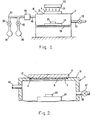
- FIG. 1 is a schematic diagram of one photochemical vapor deposition system embodying the present invention.
- FIG. 2 is a schematic diagram showing the details of the coated quartz window of FIG. 1. i
- FIG. 1 shows, in simplified form, one photochemical vapor deposition system incorporating the coated quartz window in accordance with the present invention. The reaction chamber 3, which may be formed of stainless steel, aluminum, or other suitable structural material, has a window 4 which is made integral with the top surface of the reaction chamber 3 as described in further detail with reference to FIG. 2. The window 4 is formed of a material which is transmissive to the selected wavelength of radiation used to initiate the desired photochemical reaction, such as quartz. This
radiation 20 is produced by the radiation-producingmeans 22 which may be, for example, an array of low pressure mercury vapor arc lamps. The internal face of the quartz window 4 is coated with a film of a predetermined material as described in greater detail with respect to FIG. 2. - Within the reaction chamber 3, there is a
substrate holder 24, which holds thesubstrate 26 onto which a layer of a selected material is to be deposited. Thesubstrate 26 may be formed of any material which is capable of being subjected to a photochemical vapor deposition reaction. External to the reaction chamber 3 at the bottom surface thereof, there areheating elements 28 which are used to heat thesubstrate 26 to the required temperature so that appropriate film properties, such as density, may be obtained. Atube 30 leads from the reaction chamber 3 and passes through avalve 32 and then to a vacuum-producing means (not shown). - External to the reaction chamber 3, there are placed the
chambers chambers valves tube 42. The reactant gases flow through thetube 42 into achamber 44 which contains a pool of mercury having mercury vapor above it. The reactant gases thus become mixed in thechamber 44 with mercury vapor and this reactant gas mixture then passes through thetube 46 into the reaction chamber 3, where the photochemical reaction may be brought about. - The components of the apparatus shown in FIG. 1 may be constructed of stainless steel or aluminum unless otherwise specified.
- The reaction chamber 3 with the flat quartz window 4 integral with the top surface thereof as shown in FIG. 1 is but one example of a reaction chamber embodying the present invention. Alternatively, the reaction chamber 3 may have any configuration in which at least a portion thereof is formed of quartz or other material which is transmissive to the selected wavelength of radiation, to allow this radiation to enter the reaction chamber. For example, the reaction chamber 3 may comprise a hollow quartz tube with the entire internal surface or a selected portion thereof coated with the predetermined radiation-transparent, low surface energy material in accordance with the present invention, as described in relation to FIG. 2.
- Furthermore, in addition to being used in a mercury-sensitized photochemical vapor deposition process of the type described above with respect to silicon nitride, the present invention may also be used in a photochemical vapor deposition process in which a reactant gas is directly dissociated by photo-excitation, without the use of a mercury sensitizer. In such a direct dissociation process, the apparatus is the same as that described in relation to FIG. 1 with the deletion of the
chamber 44 for containing the mercury. - Attention is now directed to FIG. 2 for a more particular consideration of the quartz window 4. Prior to insertion of the quartz window 4 into the reaction chamber 3 as shown in FIG. 2, a layer or film of a predetermined material is deposited on one surface of the quartz window 4, which will ultimately become the
internal face 5 of the quartz window 4 when the quartz window 4 is incorporated into the chamber 3 as shown in FIG. 2. (The term "internal face" of the quartz window is used herein to mean that face of the quartz window which is internal to the reaction chamber.) This predetermined material is selected to be transparent to the selected wavelength of radiation used to initiate the desired photochemical reaction, and further, to have a relatively low adhesive affinity for the material to be deposited on the substrate. The term "adhesive affinity" is used herein to mean the probability for attraction and adhesion of-the photochemical reaction products or fragments thereof on the predetermined material. In addition, this predetermined material must be stable at the elevated temperature required for the deposition reaction and must have sufficiently low vapor pressure so as not to significantly increase the evacuation time nor to produce contamination of the deposited layer. One such material which may be used is a perfluorinated polyether, i.e. a polymer with repeating ether linkages (-C-O-C-bonds) and carbon atoms saturated with fluorine. One particular perfluoropolyether which may be used is a compound sold under the trademark name Fomblin Y25 by the Montecatini-Edison Company. A layer or film of the predetermined material is deposited on theinternal face 5 of the quartz window 4 to a thickness in the range of 0.2 to 2.0 micrometers, for example, by spraying, painting, or rolling a solution of the Fomblin Y25 polymer in trichlorotrifluoroethane or chloroform onto theinternal face 5 and then allowing or causing the solvent to evaporate, as is known in the art of forming polymer films. Thus, the relativelythin film 6 of the predetermined material is formed on theinternal face 5 of the quartz window 4 as shown in FIG. 2. After thefilm 6 has been deposited on theinternal face 5 of the quartz window 4, the quartz window 4 is positioned on the top surface of the reaction chamber 3 as illustrated in FIG. 2, with an 0-ring 11 being placed at thejunction 12 between the quartz window 4 and thetop surface 10 of the reaction chamber 3. Then, a vacuum is formed in the reaction chamber 3 by withdrawing ambient air through thetube 30 and thevalve 32 by the vacuum-producing means (not shown), and the quartz window 4 thus becomes integral with the reaction chamber 3. (The reference designators 24, 26, and 46 shown in FIG. 2 indicate the same structures as set forth in FIG. 1 and are shown for purposes of correlating FIGS. 1 and 2.) - Using the apparatus shown in FIGS. 1 and 2 for a photochemical vapor deposition reaction, the material to be deposited, such as silicon nitride, does not adhere to film 6 of the predetermined material. It is believed that this predetermined material has a molecular structure and surface energy such that this predetermined material has a low adhesive affinity for the material to be deposited on the substrate. The
film 6 of the predetermined material prevents reactant gases from coming in contact with theinternal face 5 of the quartz window 4 and, further, prevents extraneous and unwanted deposits from forming either on theinternal face 5 of the quartz window or immediately in front of this internal face 5 (i.e. on thefilm 6 itseif). Consequently, theinternal face 5 of the quartz window 4 is maintained in a clean and transparent state by the process of the present invention since the accumulation of deposition products on theinternal face 5 which are opaque to reaction-inducing radiation and would attenuate, absorb, or provide a resistance to the radiation entering the deposition chamber through the quartz window 4 has been avoided. (These materials which are opaque to the reaction-inducing radiation are referred to herein as "radiation-opaque" materials). Since the rate of deposition is directly proportional to the intensity of the radiation passing through the quartz window 4, the rate of the deposition reaction is significantly increased by the process of the present invention because theinternal face 5 of the quartz window 4 is maintained in a clean and transparent state which provides continuous transmission of the reaction-inducing radiation into the reaction chamber. - Using the apparatus described in FIGS. 1 and 2, a layer of silicon'nitride was photochemically deposited on a silicon substrate by the reaction of silane, ammonia, and mercury vapor. The
source 22 of theultraviolet radiation 20 shown in FIG. 1 was an array of low pressure mercury vapor arc lamps which produced radiation having a wavelength of 2537 angstroms. Thefilm 6 was formed of Fomblin Y25 obtained from the Montecatini-Edison Company of Italy, and was a perfluorinated polyether. Thelayer 6 was formed to a thickness of approximately 4,000 to 5,000 angstroms by the spraying procedure previously described herein. A photochemical vapor deposition process was used which is similiar to that described in U.S. Patent No. 4,181,751 to T.C. Hall and J.W. Peters, assigned to the present assignee, with the optional omission of the silane pre-treatment of ammonia. The reaction chamber 3, with the coated quartz window 4 in place as shown in FIG. 2 herein, was evacuated to a pressure of 10-3 Torr. Theheating elements 28 were activated to heat thesubstrate 26 to a temperature of 150°C. - Using the apparatus and procedure just described, a layer of silicon nitride was deposited on a silicon substrate at a rate in excess of 4,000 angstroms per hour. By comparison, the deposition rate of the prior art process discussed herein is typically 50 angstroms per minute initially and decreases rapidly due to the accumulation of ultraviolet radiation-absorbing deposits on the quartz window. Deposition of the silicon nitride in such prior art processes typically ceases after approximately 45 minutes, providing a total maximum film thickness of approximately 1000 to 1400 angstroms. Thus, a significant increase in the deposition rate can be achieved by using the apparatus and process of the present invention. In addition, the process of the present invention is particularly useful for avoiding the prior art leveling-out problem during a continuous photochemical vapor deposition process, in which the amount of material deposited decreases significantly with extended processing time periods. The deposition rate of the present invention can be maintained essentially constant for a period in excess of 3 hours. In actual practice, it has been found that one polymer-coated quartz window may be used for four successive deposition processes in accordance with the process of the present invention. After such time, the polymer coating degrades and must be removed and a new polymer coating formed on the quartz window.
- While the present invention has been particularly described with respect to the preferred embodiments thereof, it will be recognized by those skilled in the-art that certain other modifications in form and detail may be made without departing from the spirit and scope of the invention. In particular, the scope of the invention is not limited to the photochemical vapor deposition of silicon nitride, which was used merely as an example, but is intended to include the photochemical vapor deposition of any material which is opaque to the radiation used to initiate or induce the photochemical reaction. In addition, it is intended to include within the scope of the present invention any process in which radiation is introduced into a reaction chamber through a transparent window, including both mercury-sensitized photochemical reactions and direct dissociation of a reactant gas or gases by photoexcitation. Moreover, the predetermined material of which the film is made may be selected as required in order to provide a film that is transparent to the wavelength of radiation necessary to initiate the desired photochemical reaction and that has a low adhesive affinity for the material to be deposited. The predetermined material may be deposited as a film onto the quartz window in accordance with known processes for forming such films and is not limited to the particular process described herein. Further, while a quartz reaction chamber window has been discussed, the reaction chamber window may be made of any material which is suitable for the desired photochemical reaction process.
- Furthermore, it is not intended to limit the process of the present invention to the particular apparatus described herein, but rather it is intended to include any method for passing radiation to a predefined enclosed region or chamber in which a photochemical vapor deposition reaction is produced, and in which the window through which the selected radiation passes into the enclosed region is protected on its inner face by a selected radiation-transmissive, low surface energy material in order to minimize the resistance to the transmission of the radiation caused by unwanted or extraneous deposition of reaction products on or immediately in front of the window.
- Finally, it is also intended to include within the scope of the present invention, a method for depositing a layer of a selected material on a substrate or target in a predetermined pattern, such as lines or stripes, rather than as a continuous film. Such deposition of a patterned layer would require that the initiating radiation for the photochemical reaction be caused to strike only selected portions of the substrate or target onto which it is desired to form a deposit. The radiation could be focused on selected portions of the target or the radiation could be passed through a mask, such as a stainless steel mask placed over the target within the reaction chamber, to cause the radiation to strike selected portions of the 'target. Optionally, a layer of the perfluoropolyether material which is used to protect the internal face of the quartz window may also be formed on the surface of the substrate in a predetermined pattern to serve as a mask during the photochemical vapor deposition of the selected material on the substrate in a predetermined pattern. As yet another option, laser radiation of the appropriate wavelength could provide the required limited and directed radiation for depositing such a patterned layer.
Claims (8)
Applications Claiming Priority (2)
| Application Number | Priority Date | Filing Date | Title |
|---|---|---|---|
| US21604180A | 1980-12-15 | 1980-12-15 | |
| US216041 | 1980-12-15 |
Publications (2)
| Publication Number | Publication Date |
|---|---|
| EP0054189A1 true EP0054189A1 (en) | 1982-06-23 |
| EP0054189B1 EP0054189B1 (en) | 1988-04-20 |
Family
ID=22805435
Family Applications (1)
| Application Number | Title | Priority Date | Filing Date |
|---|---|---|---|
| EP81109700A Expired EP0054189B1 (en) | 1980-12-15 | 1981-11-14 | Improved photochemical vapor deposition method |
Country Status (10)
| Country | Link |
|---|---|
| EP (1) | EP0054189B1 (en) |
| JP (1) | JPS57154839A (en) |
| KR (1) | KR850001974B1 (en) |
| AU (1) | AU530027B2 (en) |
| CA (1) | CA1181719A (en) |
| DE (1) | DE3176707D1 (en) |
| DK (1) | DK553981A (en) |
| GB (1) | GB2089377A (en) |
| IL (1) | IL64258A0 (en) |
| ZA (1) | ZA817910B (en) |
Cited By (4)
| Publication number | Priority date | Publication date | Assignee | Title |
|---|---|---|---|---|
| WO1986000938A1 (en) * | 1984-07-31 | 1986-02-13 | Hughes Aircraft Company | Barrel reactor and method for photochemical vapor deposition |
| EP0171605A2 (en) * | 1984-07-11 | 1986-02-19 | Hitachi, Ltd. | Method of forming an insulating film on a semiconductor body |
| EP0175456A2 (en) * | 1984-09-18 | 1986-03-26 | Kabushiki Kaisha Toshiba | Phototreating apparatus |
| WO1989007667A1 (en) * | 1988-02-09 | 1989-08-24 | Aron Vecht And Company Limited | Methods and apparatus for depositing thin films |
Families Citing this family (5)
| Publication number | Priority date | Publication date | Assignee | Title |
|---|---|---|---|---|
| DE3407089A1 (en) * | 1984-02-27 | 1985-08-29 | Siemens Ag | METHOD AND DEVICE FOR LIGHT-INDUCED, PHOTOLYTIC DEPOSITION |
| JPS6118123A (en) * | 1984-07-04 | 1986-01-27 | Semiconductor Energy Lab Co Ltd | Thin film forming apparatus |
| GB2162207B (en) * | 1984-07-26 | 1989-05-10 | Japan Res Dev Corp | Semiconductor crystal growth apparatus |
| JPS6362867A (en) * | 1986-09-02 | 1988-03-19 | Seikosha Co Ltd | Colored article |
| CN113718233A (en) * | 2021-08-30 | 2021-11-30 | 上海华力微电子有限公司 | Method for removing quartz lens |
Citations (4)
| Publication number | Priority date | Publication date | Assignee | Title |
|---|---|---|---|---|
| US3678889A (en) * | 1970-02-06 | 1972-07-25 | Tokyo Shibaura Electric Co | Reflector assembly for reflecting the vapors of high temperature volatile materials |
| US3904505A (en) * | 1970-03-20 | 1975-09-09 | Space Sciences Inc | Apparatus for film deposition |
| US3951698A (en) * | 1974-11-25 | 1976-04-20 | The United States Of America As Represented By The Secretary Of The Army | Dual use of epitaxy seed crystal as tube input window and cathode structure base |
| US3992233A (en) * | 1975-03-10 | 1976-11-16 | The Secretary Of State For Defence In Her Britannic Majesty's Government Of The United Kingdom Of Great Britain And Northern Ireland | Surface treatment of III-V compound crystals |
Family Cites Families (1)
| Publication number | Priority date | Publication date | Assignee | Title |
|---|---|---|---|---|
| US4022928A (en) * | 1975-05-22 | 1977-05-10 | Piwcyzk Bernhard P | Vacuum deposition methods and masking structure |
-
1981
- 1981-11-10 IL IL64258A patent/IL64258A0/en not_active IP Right Cessation
- 1981-11-13 GB GB8134329A patent/GB2089377A/en not_active Withdrawn
- 1981-11-14 EP EP81109700A patent/EP0054189B1/en not_active Expired
- 1981-11-14 DE DE8181109700T patent/DE3176707D1/en not_active Expired
- 1981-11-16 ZA ZA817910A patent/ZA817910B/en unknown
- 1981-11-18 CA CA000390328A patent/CA1181719A/en not_active Expired
- 1981-12-04 AU AU78255/81A patent/AU530027B2/en not_active Ceased
- 1981-12-08 KR KR1019810004788A patent/KR850001974B1/en active
- 1981-12-14 DK DK553981A patent/DK553981A/en not_active Application Discontinuation
- 1981-12-15 JP JP56201054A patent/JPS57154839A/en active Granted
Patent Citations (4)
| Publication number | Priority date | Publication date | Assignee | Title |
|---|---|---|---|---|
| US3678889A (en) * | 1970-02-06 | 1972-07-25 | Tokyo Shibaura Electric Co | Reflector assembly for reflecting the vapors of high temperature volatile materials |
| US3904505A (en) * | 1970-03-20 | 1975-09-09 | Space Sciences Inc | Apparatus for film deposition |
| US3951698A (en) * | 1974-11-25 | 1976-04-20 | The United States Of America As Represented By The Secretary Of The Army | Dual use of epitaxy seed crystal as tube input window and cathode structure base |
| US3992233A (en) * | 1975-03-10 | 1976-11-16 | The Secretary Of State For Defence In Her Britannic Majesty's Government Of The United Kingdom Of Great Britain And Northern Ireland | Surface treatment of III-V compound crystals |
Cited By (6)
| Publication number | Priority date | Publication date | Assignee | Title |
|---|---|---|---|---|
| EP0171605A2 (en) * | 1984-07-11 | 1986-02-19 | Hitachi, Ltd. | Method of forming an insulating film on a semiconductor body |
| EP0171605A3 (en) * | 1984-07-11 | 1986-06-25 | Hitachi, Ltd. | Method of manufacturing semiconductor integrated circuit involving an organic film |
| WO1986000938A1 (en) * | 1984-07-31 | 1986-02-13 | Hughes Aircraft Company | Barrel reactor and method for photochemical vapor deposition |
| EP0175456A2 (en) * | 1984-09-18 | 1986-03-26 | Kabushiki Kaisha Toshiba | Phototreating apparatus |
| EP0175456A3 (en) * | 1984-09-18 | 1987-04-29 | Kabushiki Kaisha Toshiba | Phototreating apparatus |
| WO1989007667A1 (en) * | 1988-02-09 | 1989-08-24 | Aron Vecht And Company Limited | Methods and apparatus for depositing thin films |
Also Published As
| Publication number | Publication date |
|---|---|
| GB2089377A (en) | 1982-06-23 |
| DK553981A (en) | 1982-06-16 |
| KR850001974B1 (en) | 1985-12-31 |
| AU530027B2 (en) | 1983-06-30 |
| KR830008409A (en) | 1983-11-18 |
| IL64258A0 (en) | 1982-02-28 |
| AU7825581A (en) | 1982-07-22 |
| EP0054189B1 (en) | 1988-04-20 |
| ZA817910B (en) | 1982-10-27 |
| JPS649728B2 (en) | 1989-02-20 |
| DE3176707D1 (en) | 1988-05-26 |
| JPS57154839A (en) | 1982-09-24 |
| CA1181719A (en) | 1985-01-29 |
Similar Documents
| Publication | Publication Date | Title |
|---|---|---|
| US4265932A (en) | Mobile transparent window apparatus and method for photochemical vapor deposition | |
| US4824690A (en) | Pulsed plasma process for treating a substrate | |
| EP0191855B1 (en) | Barrel reactor and method for photochemical vapor deposition | |
| US4268711A (en) | Method and apparatus for forming films from vapors using a contained plasma source | |
| US4597986A (en) | Method for photochemical vapor deposition | |
| JPH03257182A (en) | Surface processing device | |
| JPS60236219A (en) | Depositing method and device using plasma produced source gas | |
| US4058638A (en) | Method of optical thin film coating | |
| EP0054189A1 (en) | Improved photochemical vapor deposition method | |
| US3939798A (en) | Optical thin film coater | |
| DE69209163T2 (en) | Plasma assisted diamond manufacturing | |
| Schoenholtz et al. | Plasma-enhanced deposition of silicon oxynitride films | |
| JPS60245217A (en) | Thin film formation equipment | |
| US4933207A (en) | Laser and thermal assisted chemical vapor deposition of mercury containing compounds | |
| JPH0480116B2 (en) | ||
| JPS59208065A (en) | Depositing method of metal by laser | |
| JPS629189B2 (en) | ||
| JPS6046372A (en) | Thin film forming method | |
| SU901352A1 (en) | Coating device | |
| JPS60178622A (en) | Manufacture of semiconductor device | |
| JPS60236215A (en) | Laser cvd method | |
| RU2017191C1 (en) | Method of forming of mask masking layer | |
| JPS6118125A (en) | Thin film forming apparatus | |
| JPS6118124A (en) | Thin film forming apparatus | |
| JPH0257145B2 (en) |
Legal Events
| Date | Code | Title | Description |
|---|---|---|---|
| PUAI | Public reference made under article 153(3) epc to a published international application that has entered the european phase |
Free format text: ORIGINAL CODE: 0009012 |
|
| AK | Designated contracting states |
Designated state(s): CH DE FR IT LI NL SE |
|
| 17P | Request for examination filed |
Effective date: 19821209 |
|
| RAP1 | Party data changed (applicant data changed or rights of an application transferred) |
Owner name: HUGHES AIRCRAFT COMPANY |
|
| ITF | It: translation for a ep patent filed |
Owner name: SOCIETA' ITALIANA BREVETTI S.P.A. |
|
| GRAA | (expected) grant |
Free format text: ORIGINAL CODE: 0009210 |
|
| AK | Designated contracting states |
Kind code of ref document: B1 Designated state(s): CH DE FR IT LI NL SE |
|
| REF | Corresponds to: |
Ref document number: 3176707 Country of ref document: DE Date of ref document: 19880526 |
|
| ET | Fr: translation filed | ||
| PG25 | Lapsed in a contracting state [announced via postgrant information from national office to epo] |
Ref country code: SE Effective date: 19881115 |
|
| PLBE | No opposition filed within time limit |
Free format text: ORIGINAL CODE: 0009261 |
|
| STAA | Information on the status of an ep patent application or granted ep patent |
Free format text: STATUS: NO OPPOSITION FILED WITHIN TIME LIMIT |
|
| 26N | No opposition filed | ||
| PGFP | Annual fee paid to national office [announced via postgrant information from national office to epo] |
Ref country code: FR Payment date: 19941007 Year of fee payment: 14 |
|
| PGFP | Annual fee paid to national office [announced via postgrant information from national office to epo] |
Ref country code: DE Payment date: 19941024 Year of fee payment: 14 |
|
| PGFP | Annual fee paid to national office [announced via postgrant information from national office to epo] |
Ref country code: CH Payment date: 19941025 Year of fee payment: 14 |
|
| PGFP | Annual fee paid to national office [announced via postgrant information from national office to epo] |
Ref country code: NL Payment date: 19941130 Year of fee payment: 14 |
|
| EUG | Se: european patent has lapsed |
Ref document number: 81109700.5 Effective date: 19890726 |
|
| PG25 | Lapsed in a contracting state [announced via postgrant information from national office to epo] |
Ref country code: LI Effective date: 19951130 Ref country code: CH Effective date: 19951130 |
|
| PG25 | Lapsed in a contracting state [announced via postgrant information from national office to epo] |
Ref country code: NL Effective date: 19960601 |
|
| REG | Reference to a national code |
Ref country code: CH Ref legal event code: PL |
|
| PG25 | Lapsed in a contracting state [announced via postgrant information from national office to epo] |
Ref country code: FR Effective date: 19960731 |
|
| NLV4 | Nl: lapsed or anulled due to non-payment of the annual fee |
Effective date: 19960601 |
|
| PG25 | Lapsed in a contracting state [announced via postgrant information from national office to epo] |
Ref country code: DE Effective date: 19960801 |
|
| REG | Reference to a national code |
Ref country code: FR Ref legal event code: ST |